US6048751A - Process for manufacture of composite semiconductor devices - Google Patents
Process for manufacture of composite semiconductor devicesDownload PDFInfo
- Publication number
- US6048751A US6048751AUS08/572,275US57227595AUS6048751AUS 6048751 AUS6048751 AUS 6048751AUS 57227595 AUS57227595 AUS 57227595AUS 6048751 AUS6048751 AUS 6048751A
- Authority
- US
- United States
- Prior art keywords
- semiconductor device
- substrate
- cement
- conductors
- modulator
- Prior art date
- Legal status (The legal status is an assumption and is not a legal conclusion. Google has not performed a legal analysis and makes no representation as to the accuracy of the status listed.)
- Expired - Lifetime
Links
- 239000004065semiconductorSubstances0.000titleclaimsabstractdescription40
- 238000000034methodMethods0.000titleclaimsdescription27
- 230000008569processEffects0.000titledescription8
- 238000004519manufacturing processMethods0.000titledescription5
- 239000002131composite materialSubstances0.000title1
- 239000000758substrateSubstances0.000claimsabstractdescription62
- 239000004568cementSubstances0.000claimsabstractdescription47
- 239000004593EpoxySubstances0.000claimsabstractdescription31
- 229910001218Gallium arsenideInorganic materials0.000claimsabstractdescription21
- 239000004020conductorSubstances0.000claimsabstractdescription19
- 229910000980Aluminium gallium arsenideInorganic materials0.000claimsabstractdescription13
- 229910052737goldInorganic materials0.000claimsdescription7
- 229910052738indiumInorganic materials0.000claimsdescription7
- 239000000203mixtureSubstances0.000claimsdescription2
- 229910052718tinInorganic materials0.000claimsdescription2
- 229910052745leadInorganic materials0.000claims1
- 229910052710siliconInorganic materials0.000description19
- XUIMIQQOPSSXEZ-UHFFFAOYSA-NSiliconChemical compound[Si]XUIMIQQOPSSXEZ-UHFFFAOYSA-N0.000description18
- 239000010703siliconSubstances0.000description18
- 230000008901benefitEffects0.000description8
- 230000003287optical effectEffects0.000description8
- 229920002120photoresistant polymerPolymers0.000description8
- 101150114166coa2 geneProteins0.000description6
- 239000010931goldSubstances0.000description6
- 239000007788liquidSubstances0.000description6
- 101100275282Arabidopsis thaliana COI1 geneProteins0.000description5
- 101150030370COI2 geneProteins0.000description5
- 102100030978Cytochrome c oxidase assembly factor 1 homologHuman genes0.000description5
- 101000919635Homo sapiens Cytochrome c oxidase assembly factor 1 homologProteins0.000description5
- 101100275280Oryza sativa subsp. japonica COI1A geneProteins0.000description5
- 238000003491arrayMethods0.000description5
- VYPSYNLAJGMNEJ-UHFFFAOYSA-NSilicium dioxideChemical compoundO=[Si]=OVYPSYNLAJGMNEJ-UHFFFAOYSA-N0.000description4
- 239000011248coating agentSubstances0.000description4
- 238000000576coating methodMethods0.000description4
- 238000000151depositionMethods0.000description4
- PCHJSUWPFVWCPO-UHFFFAOYSA-NgoldChemical compound[Au]PCHJSUWPFVWCPO-UHFFFAOYSA-N0.000description4
- APFVFJFRJDLVQX-UHFFFAOYSA-Nindium atomChemical compound[In]APFVFJFRJDLVQX-UHFFFAOYSA-N0.000description4
- 229910052581Si3N4Inorganic materials0.000description3
- 239000011324beadSubstances0.000description3
- 238000004891communicationMethods0.000description3
- 125000003700epoxy groupChemical group0.000description3
- 238000005530etchingMethods0.000description3
- 239000000835fiberSubstances0.000description3
- 229910010272inorganic materialInorganic materials0.000description3
- 239000011147inorganic materialSubstances0.000description3
- 230000010354integrationEffects0.000description3
- 239000000463materialSubstances0.000description3
- 229920000647polyepoxidePolymers0.000description3
- 229920000642polymerPolymers0.000description3
- HQVNEWCFYHHQES-UHFFFAOYSA-Nsilicon nitrideChemical compoundN12[Si]34N5[Si]62N3[Si]51N64HQVNEWCFYHHQES-UHFFFAOYSA-N0.000description3
- 229910052814silicon oxideInorganic materials0.000description3
- 125000006850spacer groupChemical group0.000description3
- 230000015572biosynthetic processEffects0.000description2
- 230000008021depositionEffects0.000description2
- 230000006870functionEffects0.000description2
- 238000009396hybridizationMethods0.000description2
- 230000010365information processingEffects0.000description2
- 239000007787solidSubstances0.000description2
- 239000002904solventSubstances0.000description2
- 239000000126substanceSubstances0.000description2
- 239000004642PolyimideSubstances0.000description1
- 229920002472StarchPolymers0.000description1
- 238000010521absorption reactionMethods0.000description1
- 229920006397acrylic thermoplasticPolymers0.000description1
- 230000009471actionEffects0.000description1
- 238000007605air dryingMethods0.000description1
- 230000004888barrier functionEffects0.000description1
- 230000009286beneficial effectEffects0.000description1
- UMIVXZPTRXBADB-UHFFFAOYSA-NbenzocyclobuteneChemical classC1=CC=C2CCC2=C1UMIVXZPTRXBADB-UHFFFAOYSA-N0.000description1
- 230000005540biological transmissionEffects0.000description1
- 238000005229chemical vapour depositionMethods0.000description1
- 239000003245coalSubstances0.000description1
- 230000000295complement effectEffects0.000description1
- 238000010586diagramMethods0.000description1
- 238000007598dipping methodMethods0.000description1
- 238000005516engineering processMethods0.000description1
- 238000011049fillingMethods0.000description1
- 238000010438heat treatmentMethods0.000description1
- 238000005304joiningMethods0.000description1
- 238000002844meltingMethods0.000description1
- 230000008018meltingEffects0.000description1
- 238000002156mixingMethods0.000description1
- 239000013307optical fiberSubstances0.000description1
- 239000011368organic materialSubstances0.000description1
- 238000000059patterningMethods0.000description1
- 229920003229poly(methyl methacrylate)Polymers0.000description1
- 229920001721polyimidePolymers0.000description1
- 235000012239silicon dioxideNutrition0.000description1
- 239000000377silicon dioxideSubstances0.000description1
- LIVNPJMFVYWSIS-UHFFFAOYSA-Nsilicon monoxideChemical class[Si-]#[O+]LIVNPJMFVYWSIS-UHFFFAOYSA-N0.000description1
- 229910000679solderInorganic materials0.000description1
- 239000011343solid materialSubstances0.000description1
- 239000008107starchSubstances0.000description1
- 235000019698starchNutrition0.000description1
- ISXSCDLOGDJUNJ-UHFFFAOYSA-Ntert-butyl prop-2-enoateChemical compoundCC(C)(C)OC(=O)C=CISXSCDLOGDJUNJ-UHFFFAOYSA-N0.000description1
- 229920001169thermoplasticPolymers0.000description1
- 229920001187thermosetting polymerPolymers0.000description1
- 239000004416thermosoftening plasticSubstances0.000description1
- 150000003673urethanesChemical class0.000description1
Images


Classifications
- H—ELECTRICITY
- H01—ELECTRIC ELEMENTS
- H01L—SEMICONDUCTOR DEVICES NOT COVERED BY CLASS H10
- H01L25/00—Assemblies consisting of a plurality of semiconductor or other solid state devices
- H01L25/16—Assemblies consisting of a plurality of semiconductor or other solid state devices the devices being of types provided for in two or more different subclasses of H10B, H10D, H10F, H10H, H10K or H10N, e.g. forming hybrid circuits
- H01L25/167—Assemblies consisting of a plurality of semiconductor or other solid state devices the devices being of types provided for in two or more different subclasses of H10B, H10D, H10F, H10H, H10K or H10N, e.g. forming hybrid circuits comprising optoelectronic devices, e.g. LED, photodiodes
- H—ELECTRICITY
- H10—SEMICONDUCTOR DEVICES; ELECTRIC SOLID-STATE DEVICES NOT OTHERWISE PROVIDED FOR
- H10F—INORGANIC SEMICONDUCTOR DEVICES SENSITIVE TO INFRARED RADIATION, LIGHT, ELECTROMAGNETIC RADIATION OF SHORTER WAVELENGTH OR CORPUSCULAR RADIATION
- H10F55/00—Radiation-sensitive semiconductor devices covered by groups H10F10/00, H10F19/00 or H10F30/00 being structurally associated with electric light sources and electrically or optically coupled thereto
- H10F55/18—Radiation-sensitive semiconductor devices covered by groups H10F10/00, H10F19/00 or H10F30/00 being structurally associated with electric light sources and electrically or optically coupled thereto wherein the radiation-sensitive semiconductor devices and the electric light source share a common body having dual-functionality of light emission and light detection
- H—ELECTRICITY
- H01—ELECTRIC ELEMENTS
- H01L—SEMICONDUCTOR DEVICES NOT COVERED BY CLASS H10
- H01L2221/00—Processes or apparatus adapted for the manufacture or treatment of semiconductor or solid state devices or of parts thereof covered by H01L21/00
- H01L2221/67—Apparatus for handling semiconductor or electric solid state devices during manufacture or treatment thereof; Apparatus for handling wafers during manufacture or treatment of semiconductor or electric solid state devices or components; Apparatus not specifically provided for elsewhere
- H01L2221/683—Apparatus for handling semiconductor or electric solid state devices during manufacture or treatment thereof; Apparatus for handling wafers during manufacture or treatment of semiconductor or electric solid state devices or components; Apparatus not specifically provided for elsewhere for supporting or gripping
- H01L2221/68304—Apparatus for handling semiconductor or electric solid state devices during manufacture or treatment thereof; Apparatus for handling wafers during manufacture or treatment of semiconductor or electric solid state devices or components; Apparatus not specifically provided for elsewhere for supporting or gripping using temporarily an auxiliary support
- H01L2221/68359—Apparatus for handling semiconductor or electric solid state devices during manufacture or treatment thereof; Apparatus for handling wafers during manufacture or treatment of semiconductor or electric solid state devices or components; Apparatus not specifically provided for elsewhere for supporting or gripping using temporarily an auxiliary support used as a support during manufacture of interconnect decals or build up layers
- H—ELECTRICITY
- H01—ELECTRIC ELEMENTS
- H01L—SEMICONDUCTOR DEVICES NOT COVERED BY CLASS H10
- H01L2221/00—Processes or apparatus adapted for the manufacture or treatment of semiconductor or solid state devices or of parts thereof covered by H01L21/00
- H01L2221/67—Apparatus for handling semiconductor or electric solid state devices during manufacture or treatment thereof; Apparatus for handling wafers during manufacture or treatment of semiconductor or electric solid state devices or components; Apparatus not specifically provided for elsewhere
- H01L2221/683—Apparatus for handling semiconductor or electric solid state devices during manufacture or treatment thereof; Apparatus for handling wafers during manufacture or treatment of semiconductor or electric solid state devices or components; Apparatus not specifically provided for elsewhere for supporting or gripping
- H01L2221/68304—Apparatus for handling semiconductor or electric solid state devices during manufacture or treatment thereof; Apparatus for handling wafers during manufacture or treatment of semiconductor or electric solid state devices or components; Apparatus not specifically provided for elsewhere for supporting or gripping using temporarily an auxiliary support
- H01L2221/68363—Apparatus for handling semiconductor or electric solid state devices during manufacture or treatment thereof; Apparatus for handling wafers during manufacture or treatment of semiconductor or electric solid state devices or components; Apparatus not specifically provided for elsewhere for supporting or gripping using temporarily an auxiliary support used in a transfer process involving transfer directly from an origin substrate to a target substrate without use of an intermediate handle substrate
- H—ELECTRICITY
- H01—ELECTRIC ELEMENTS
- H01L—SEMICONDUCTOR DEVICES NOT COVERED BY CLASS H10
- H01L2224/00—Indexing scheme for arrangements for connecting or disconnecting semiconductor or solid-state bodies and methods related thereto as covered by H01L24/00
- H01L2224/01—Means for bonding being attached to, or being formed on, the surface to be connected, e.g. chip-to-package, die-attach, "first-level" interconnects; Manufacturing methods related thereto
- H01L2224/10—Bump connectors; Manufacturing methods related thereto
- H01L2224/15—Structure, shape, material or disposition of the bump connectors after the connecting process
- H01L2224/16—Structure, shape, material or disposition of the bump connectors after the connecting process of an individual bump connector
- H01L2224/161—Disposition
- H01L2224/16151—Disposition the bump connector connecting between a semiconductor or solid-state body and an item not being a semiconductor or solid-state body, e.g. chip-to-substrate, chip-to-passive
- H01L2224/16221—Disposition the bump connector connecting between a semiconductor or solid-state body and an item not being a semiconductor or solid-state body, e.g. chip-to-substrate, chip-to-passive the body and the item being stacked
- H01L2224/16225—Disposition the bump connector connecting between a semiconductor or solid-state body and an item not being a semiconductor or solid-state body, e.g. chip-to-substrate, chip-to-passive the body and the item being stacked the item being non-metallic, e.g. insulating substrate with or without metallisation
- H—ELECTRICITY
- H01—ELECTRIC ELEMENTS
- H01L—SEMICONDUCTOR DEVICES NOT COVERED BY CLASS H10
- H01L2924/00—Indexing scheme for arrangements or methods for connecting or disconnecting semiconductor or solid-state bodies as covered by H01L24/00
- H01L2924/0001—Technical content checked by a classifier
- H01L2924/00014—Technical content checked by a classifier the subject-matter covered by the group, the symbol of which is combined with the symbol of this group, being disclosed without further technical details
- H—ELECTRICITY
- H01—ELECTRIC ELEMENTS
- H01L—SEMICONDUCTOR DEVICES NOT COVERED BY CLASS H10
- H01L2924/00—Indexing scheme for arrangements or methods for connecting or disconnecting semiconductor or solid-state bodies as covered by H01L24/00
- H01L2924/10—Details of semiconductor or other solid state devices to be connected
- H01L2924/102—Material of the semiconductor or solid state bodies
- H01L2924/1025—Semiconducting materials
- H01L2924/10251—Elemental semiconductors, i.e. Group IV
- H01L2924/10253—Silicon [Si]
Definitions
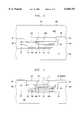
- Yet another embodiment of the inventioninvolves selective photo-chemical removal of the cement CM1 at the bond pads.
- GaAs/AlGaAs multiple quantum well modulatorsare their typical operation at 850 nm. This short wavelength allows the formation of small optical spots whose potential spot sizes vary with the wavelength.
- the contacts on each semiconductor deviceneed not be coplanar, as long as they complement the heights of the Si-mounted contacts to which they are to be bonded.
- the bonding materialneed not be indium (In).
- the contactsare gold, or various mixtures of In, Au, Sn, and/or Pb.
Landscapes
- Engineering & Computer Science (AREA)
- Microelectronics & Electronic Packaging (AREA)
- Physics & Mathematics (AREA)
- Condensed Matter Physics & Semiconductors (AREA)
- General Physics & Mathematics (AREA)
- Computer Hardware Design (AREA)
- Power Engineering (AREA)
- Optical Integrated Circuits (AREA)
Abstract
Description
Claims (10)
Priority Applications (2)
| Application Number | Priority Date | Filing Date | Title |
|---|---|---|---|
| US08/572,275US6048751A (en) | 1993-06-25 | 1995-12-13 | Process for manufacture of composite semiconductor devices |
| US09/547,122US6444491B1 (en) | 1993-06-25 | 2000-04-11 | Composite semiconductor devices and method for manufacture thereof |
Applications Claiming Priority (4)
| Application Number | Priority Date | Filing Date | Title |
|---|---|---|---|
| US08/083,742US5385632A (en) | 1993-06-25 | 1993-06-25 | Method for manufacturing integrated semiconductor devices |
| US23630794A | 1994-05-02 | 1994-05-02 | |
| US08/366,864US5578162A (en) | 1993-06-25 | 1994-12-30 | Integrated composite semiconductor devices and method for manufacture thereof |
| US08/572,275US6048751A (en) | 1993-06-25 | 1995-12-13 | Process for manufacture of composite semiconductor devices |
Related Parent Applications (1)
| Application Number | Title | Priority Date | Filing Date |
|---|---|---|---|
| US08/366,864Continuation-In-PartUS5578162A (en) | 1993-06-25 | 1994-12-30 | Integrated composite semiconductor devices and method for manufacture thereof |
Related Child Applications (1)
| Application Number | Title | Priority Date | Filing Date |
|---|---|---|---|
| US09/547,122DivisionUS6444491B1 (en) | 1993-06-25 | 2000-04-11 | Composite semiconductor devices and method for manufacture thereof |
Publications (1)
| Publication Number | Publication Date |
|---|---|
| US6048751Atrue US6048751A (en) | 2000-04-11 |
Family
ID=27491820
Family Applications (2)
| Application Number | Title | Priority Date | Filing Date |
|---|---|---|---|
| US08/572,275Expired - LifetimeUS6048751A (en) | 1993-06-25 | 1995-12-13 | Process for manufacture of composite semiconductor devices |
| US09/547,122Expired - Fee RelatedUS6444491B1 (en) | 1993-06-25 | 2000-04-11 | Composite semiconductor devices and method for manufacture thereof |
Family Applications After (1)
| Application Number | Title | Priority Date | Filing Date |
|---|---|---|---|
| US09/547,122Expired - Fee RelatedUS6444491B1 (en) | 1993-06-25 | 2000-04-11 | Composite semiconductor devices and method for manufacture thereof |
Country Status (1)
| Country | Link |
|---|---|
| US (2) | US6048751A (en) |
Cited By (44)
| Publication number | Priority date | Publication date | Assignee | Title |
|---|---|---|---|---|
| US20030011851A1 (en)* | 2001-06-29 | 2003-01-16 | John Trezza | Redundant optical device array |
| WO2003010771A1 (en)* | 2001-07-23 | 2003-02-06 | Motorola, Inc. A Corporation Of The State Of Delaware | Memory system with independently accessible memory subsystems |
| US6589856B2 (en) | 2001-08-06 | 2003-07-08 | Motorola, Inc. | Method and apparatus for controlling anti-phase domains in semiconductor structures and devices |
| US6620642B2 (en) | 2001-06-29 | 2003-09-16 | Xanoptix, Inc. | Opto-electronic device integration |
| US6633421B2 (en) | 2001-06-29 | 2003-10-14 | Xanoptrix, Inc. | Integrated arrays of modulators and lasers on electronics |
| US6639249B2 (en) | 2001-08-06 | 2003-10-28 | Motorola, Inc. | Structure and method for fabrication for a solid-state lighting device |
| US6638838B1 (en) | 2000-10-02 | 2003-10-28 | Motorola, Inc. | Semiconductor structure including a partially annealed layer and method of forming the same |
| US20030207589A1 (en)* | 2002-05-03 | 2003-11-06 | Thoughtbeam, Inc. | Method for growing a monocrystalline oxide layer and for fabricating a semiconductor device on a monocrystalline substrate |
| US6646293B2 (en) | 2001-07-18 | 2003-11-11 | Motorola, Inc. | Structure for fabricating high electron mobility transistors utilizing the formation of complaint substrates |
| US6667196B2 (en) | 2001-07-25 | 2003-12-23 | Motorola, Inc. | Method for real-time monitoring and controlling perovskite oxide film growth and semiconductor structure formed using the method |
| US6673646B2 (en) | 2001-02-28 | 2004-01-06 | Motorola, Inc. | Growth of compound semiconductor structures on patterned oxide films and process for fabricating same |
| US6673667B2 (en) | 2001-08-15 | 2004-01-06 | Motorola, Inc. | Method for manufacturing a substantially integral monolithic apparatus including a plurality of semiconductor materials |
| US6693033B2 (en) | 2000-02-10 | 2004-02-17 | Motorola, Inc. | Method of removing an amorphous oxide from a monocrystalline surface |
| US6693298B2 (en) | 2001-07-20 | 2004-02-17 | Motorola, Inc. | Structure and method for fabricating epitaxial semiconductor on insulator (SOI) structures and devices utilizing the formation of a compliant substrate for materials used to form same |
| US6709989B2 (en) | 2001-06-21 | 2004-03-23 | Motorola, Inc. | Method for fabricating a semiconductor structure including a metal oxide interface with silicon |
| US6724794B2 (en) | 2001-06-29 | 2004-04-20 | Xanoptix, Inc. | Opto-electronic device integration |
| US6731665B2 (en) | 2001-06-29 | 2004-05-04 | Xanoptix Inc. | Laser arrays for high power fiber amplifier pumps |
| US6753199B2 (en) | 2001-06-29 | 2004-06-22 | Xanoptix, Inc. | Topside active optical device apparatus and method |
| US6753197B2 (en) | 2001-06-29 | 2004-06-22 | Xanoptix, Inc. | Opto-electronic device integration |
| US6775308B2 (en) | 2001-06-29 | 2004-08-10 | Xanoptix, Inc. | Multi-wavelength semiconductor laser arrays and applications thereof |
| US6790691B2 (en) | 2001-06-29 | 2004-09-14 | Xanoptix, Inc. | Opto-electronic device integration |
| US6855992B2 (en) | 2001-07-24 | 2005-02-15 | Motorola Inc. | Structure and method for fabricating configurable transistor devices utilizing the formation of a compliant substrate for materials used to form the same |
| US6885065B2 (en) | 2002-11-20 | 2005-04-26 | Freescale Semiconductor, Inc. | Ferromagnetic semiconductor structure and method for forming the same |
| US6965128B2 (en) | 2003-02-03 | 2005-11-15 | Freescale Semiconductor, Inc. | Structure and method for fabricating semiconductor microresonator devices |
| US6992321B2 (en) | 2001-07-13 | 2006-01-31 | Motorola, Inc. | Structure and method for fabricating semiconductor structures and devices utilizing piezoelectric materials |
| US7005717B2 (en) | 2000-05-31 | 2006-02-28 | Freescale Semiconductor, Inc. | Semiconductor device and method |
| US7019332B2 (en) | 2001-07-20 | 2006-03-28 | Freescale Semiconductor, Inc. | Fabrication of a wavelength locker within a semiconductor structure |
| US7020374B2 (en) | 2003-02-03 | 2006-03-28 | Freescale Semiconductor, Inc. | Optical waveguide structure and method for fabricating the same |
| US7045815B2 (en) | 2001-04-02 | 2006-05-16 | Freescale Semiconductor, Inc. | Semiconductor structure exhibiting reduced leakage current and method of fabricating same |
| US7067856B2 (en) | 2000-02-10 | 2006-06-27 | Freescale Semiconductor, Inc. | Semiconductor structure, semiconductor device, communicating device, integrated circuit, and process for fabricating the same |
| US7105866B2 (en) | 2000-07-24 | 2006-09-12 | Freescale Semiconductor, Inc. | Heterojunction tunneling diodes and process for fabricating same |
| US7161227B2 (en) | 2001-08-14 | 2007-01-09 | Motorola, Inc. | Structure and method for fabricating semiconductor structures and devices for detecting an object |
| US7169619B2 (en) | 2002-11-19 | 2007-01-30 | Freescale Semiconductor, Inc. | Method for fabricating semiconductor structures on vicinal substrates using a low temperature, low pressure, alkaline earth metal-rich process |
| US7211852B2 (en) | 2001-01-19 | 2007-05-01 | Freescale Semiconductor, Inc. | Structure and method for fabricating GaN devices utilizing the formation of a compliant substrate |
| US7342276B2 (en) | 2001-10-17 | 2008-03-11 | Freescale Semiconductor, Inc. | Method and apparatus utilizing monocrystalline insulator |
| CN100442527C (en)* | 2004-12-09 | 2008-12-10 | 璨圆光电股份有限公司 | Semiconductor photodetector |
| DE102016125430A1 (en)* | 2016-12-22 | 2018-06-28 | Osram Opto Semiconductors Gmbh | Surface-mountable semiconductor laser, arrangement with such a semiconductor laser and operating method therefor |
| US20220173157A1 (en)* | 2019-04-23 | 2022-06-02 | Osram Opto Semiconductors Gmbh | µ-Led, µ-Led Device, Display And Method For The Same |
| US12176469B2 (en) | 2019-01-29 | 2024-12-24 | Osram Opto Semiconductors Gmbh | μ-LED, μ-LED device, display and method for the same |
| US12183261B2 (en) | 2019-01-29 | 2024-12-31 | Osram Opto Semiconductors Gmbh | Video wall, driver circuits, controls and method thereof |
| US12190788B2 (en) | 2019-01-29 | 2025-01-07 | Osram Opto Semiconductors Gmbh | μ-LED, μ-LED device, display and method for the same |
| US12189280B2 (en) | 2019-05-23 | 2025-01-07 | Osram Opto Semiconductors Gmbh | Lighting arrangement, light guide arrangement and method |
| US12261256B2 (en) | 2019-02-11 | 2025-03-25 | Osram Opto Semiconductors Gmbh | Optoelectronic component, optoelectronic arrangement and method |
| US12294039B2 (en) | 2019-09-20 | 2025-05-06 | Osram Opto Semiconductors Gmbh | Optoelectronic component, semiconductor structure and method |
Citations (4)
| Publication number | Priority date | Publication date | Assignee | Title |
|---|---|---|---|---|
| US4764804A (en)* | 1986-02-21 | 1988-08-16 | Hitachi, Ltd. | Semiconductor device and process for producing the same |
| US4954458A (en)* | 1982-06-03 | 1990-09-04 | Texas Instruments Incorporated | Method of forming a three dimensional integrated circuit structure |
| US5135878A (en)* | 1990-08-28 | 1992-08-04 | Solid State Devices, Inc. | Schottky diode |
| US5478781A (en)* | 1993-06-21 | 1995-12-26 | International Business Machines Corporation | Polyimide-insulated cube package of stacked semiconductor device chips |
Family Cites Families (2)
| Publication number | Priority date | Publication date | Assignee | Title |
|---|---|---|---|---|
| US4783594A (en)* | 1987-11-20 | 1988-11-08 | Santa Barbara Research Center | Reticular detector array |
| US5488504A (en)* | 1993-08-20 | 1996-01-30 | Martin Marietta Corp. | Hybridized asymmetric fabry-perot quantum well light modulator |
- 1995
- 1995-12-13USUS08/572,275patent/US6048751A/ennot_activeExpired - Lifetime
- 2000
- 2000-04-11USUS09/547,122patent/US6444491B1/ennot_activeExpired - Fee Related
Patent Citations (4)
| Publication number | Priority date | Publication date | Assignee | Title |
|---|---|---|---|---|
| US4954458A (en)* | 1982-06-03 | 1990-09-04 | Texas Instruments Incorporated | Method of forming a three dimensional integrated circuit structure |
| US4764804A (en)* | 1986-02-21 | 1988-08-16 | Hitachi, Ltd. | Semiconductor device and process for producing the same |
| US5135878A (en)* | 1990-08-28 | 1992-08-04 | Solid State Devices, Inc. | Schottky diode |
| US5478781A (en)* | 1993-06-21 | 1995-12-26 | International Business Machines Corporation | Polyimide-insulated cube package of stacked semiconductor device chips |
Cited By (62)
| Publication number | Priority date | Publication date | Assignee | Title |
|---|---|---|---|---|
| US6693033B2 (en) | 2000-02-10 | 2004-02-17 | Motorola, Inc. | Method of removing an amorphous oxide from a monocrystalline surface |
| US7067856B2 (en) | 2000-02-10 | 2006-06-27 | Freescale Semiconductor, Inc. | Semiconductor structure, semiconductor device, communicating device, integrated circuit, and process for fabricating the same |
| US7005717B2 (en) | 2000-05-31 | 2006-02-28 | Freescale Semiconductor, Inc. | Semiconductor device and method |
| US7105866B2 (en) | 2000-07-24 | 2006-09-12 | Freescale Semiconductor, Inc. | Heterojunction tunneling diodes and process for fabricating same |
| US6638838B1 (en) | 2000-10-02 | 2003-10-28 | Motorola, Inc. | Semiconductor structure including a partially annealed layer and method of forming the same |
| US7211852B2 (en) | 2001-01-19 | 2007-05-01 | Freescale Semiconductor, Inc. | Structure and method for fabricating GaN devices utilizing the formation of a compliant substrate |
| US6673646B2 (en) | 2001-02-28 | 2004-01-06 | Motorola, Inc. | Growth of compound semiconductor structures on patterned oxide films and process for fabricating same |
| US7045815B2 (en) | 2001-04-02 | 2006-05-16 | Freescale Semiconductor, Inc. | Semiconductor structure exhibiting reduced leakage current and method of fabricating same |
| US6709989B2 (en) | 2001-06-21 | 2004-03-23 | Motorola, Inc. | Method for fabricating a semiconductor structure including a metal oxide interface with silicon |
| US20030011851A1 (en)* | 2001-06-29 | 2003-01-16 | John Trezza | Redundant optical device array |
| US6731665B2 (en) | 2001-06-29 | 2004-05-04 | Xanoptix Inc. | Laser arrays for high power fiber amplifier pumps |
| US7831151B2 (en) | 2001-06-29 | 2010-11-09 | John Trezza | Redundant optical device array |
| US7092424B2 (en) | 2001-06-29 | 2006-08-15 | Cubic Wafer, Inc. | Integrated arrays of modulators and lasers on electronics |
| US6633421B2 (en) | 2001-06-29 | 2003-10-14 | Xanoptrix, Inc. | Integrated arrays of modulators and lasers on electronics |
| US6956244B2 (en)* | 2001-06-29 | 2005-10-18 | Xanoptix Inc. | Opto-electronic device integration |
| US6724794B2 (en) | 2001-06-29 | 2004-04-20 | Xanoptix, Inc. | Opto-electronic device integration |
| US6620642B2 (en) | 2001-06-29 | 2003-09-16 | Xanoptix, Inc. | Opto-electronic device integration |
| US6753199B2 (en) | 2001-06-29 | 2004-06-22 | Xanoptix, Inc. | Topside active optical device apparatus and method |
| US6753197B2 (en) | 2001-06-29 | 2004-06-22 | Xanoptix, Inc. | Opto-electronic device integration |
| US6775308B2 (en) | 2001-06-29 | 2004-08-10 | Xanoptix, Inc. | Multi-wavelength semiconductor laser arrays and applications thereof |
| US6790691B2 (en) | 2001-06-29 | 2004-09-14 | Xanoptix, Inc. | Opto-electronic device integration |
| US20040200573A1 (en)* | 2001-06-29 | 2004-10-14 | Greg Dudoff | Opto-electronic device integration |
| US6992321B2 (en) | 2001-07-13 | 2006-01-31 | Motorola, Inc. | Structure and method for fabricating semiconductor structures and devices utilizing piezoelectric materials |
| US6646293B2 (en) | 2001-07-18 | 2003-11-11 | Motorola, Inc. | Structure for fabricating high electron mobility transistors utilizing the formation of complaint substrates |
| US7019332B2 (en) | 2001-07-20 | 2006-03-28 | Freescale Semiconductor, Inc. | Fabrication of a wavelength locker within a semiconductor structure |
| US6693298B2 (en) | 2001-07-20 | 2004-02-17 | Motorola, Inc. | Structure and method for fabricating epitaxial semiconductor on insulator (SOI) structures and devices utilizing the formation of a compliant substrate for materials used to form same |
| WO2003010771A1 (en)* | 2001-07-23 | 2003-02-06 | Motorola, Inc. A Corporation Of The State Of Delaware | Memory system with independently accessible memory subsystems |
| US6855992B2 (en) | 2001-07-24 | 2005-02-15 | Motorola Inc. | Structure and method for fabricating configurable transistor devices utilizing the formation of a compliant substrate for materials used to form the same |
| US6667196B2 (en) | 2001-07-25 | 2003-12-23 | Motorola, Inc. | Method for real-time monitoring and controlling perovskite oxide film growth and semiconductor structure formed using the method |
| US6589856B2 (en) | 2001-08-06 | 2003-07-08 | Motorola, Inc. | Method and apparatus for controlling anti-phase domains in semiconductor structures and devices |
| US6639249B2 (en) | 2001-08-06 | 2003-10-28 | Motorola, Inc. | Structure and method for fabrication for a solid-state lighting device |
| US7161227B2 (en) | 2001-08-14 | 2007-01-09 | Motorola, Inc. | Structure and method for fabricating semiconductor structures and devices for detecting an object |
| US6673667B2 (en) | 2001-08-15 | 2004-01-06 | Motorola, Inc. | Method for manufacturing a substantially integral monolithic apparatus including a plurality of semiconductor materials |
| US7342276B2 (en) | 2001-10-17 | 2008-03-11 | Freescale Semiconductor, Inc. | Method and apparatus utilizing monocrystalline insulator |
| US6916717B2 (en) | 2002-05-03 | 2005-07-12 | Motorola, Inc. | Method for growing a monocrystalline oxide layer and for fabricating a semiconductor device on a monocrystalline substrate |
| US20030207589A1 (en)* | 2002-05-03 | 2003-11-06 | Thoughtbeam, Inc. | Method for growing a monocrystalline oxide layer and for fabricating a semiconductor device on a monocrystalline substrate |
| US7169619B2 (en) | 2002-11-19 | 2007-01-30 | Freescale Semiconductor, Inc. | Method for fabricating semiconductor structures on vicinal substrates using a low temperature, low pressure, alkaline earth metal-rich process |
| US6885065B2 (en) | 2002-11-20 | 2005-04-26 | Freescale Semiconductor, Inc. | Ferromagnetic semiconductor structure and method for forming the same |
| US7020374B2 (en) | 2003-02-03 | 2006-03-28 | Freescale Semiconductor, Inc. | Optical waveguide structure and method for fabricating the same |
| US6965128B2 (en) | 2003-02-03 | 2005-11-15 | Freescale Semiconductor, Inc. | Structure and method for fabricating semiconductor microresonator devices |
| CN100442527C (en)* | 2004-12-09 | 2008-12-10 | 璨圆光电股份有限公司 | Semiconductor photodetector |
| DE102016125430A1 (en)* | 2016-12-22 | 2018-06-28 | Osram Opto Semiconductors Gmbh | Surface-mountable semiconductor laser, arrangement with such a semiconductor laser and operating method therefor |
| US10833476B2 (en) | 2016-12-22 | 2020-11-10 | Osram Oled Gmbh | Surface-mountable semiconductor laser, arrangement with such a semiconductor laser and operating method for same |
| US12198606B2 (en) | 2019-01-13 | 2025-01-14 | Osram Opto Semiconductors Gmbh | μ-LED, μ-LED device, display and method for the same |
| US12199219B2 (en) | 2019-01-29 | 2025-01-14 | Osram Opto Semiconductors Gmbh | μ-LED, μ-LED device, display and method for the same |
| US12206054B2 (en) | 2019-01-29 | 2025-01-21 | Osram Opto Semiconductors Gmbh | μ-LED, μ-LED device, display and method for the same |
| US12190788B2 (en) | 2019-01-29 | 2025-01-07 | Osram Opto Semiconductors Gmbh | μ-LED, μ-LED device, display and method for the same |
| US12283648B2 (en) | 2019-01-29 | 2025-04-22 | Osram Opto Semiconductors Gmbh | μ-led, μ-led device, display and method for the same |
| US12199221B2 (en) | 2019-01-29 | 2025-01-14 | Osram Opto Semiconductors Gmbh | μ-LED, μ-LED device, display and method for the same |
| US12205521B2 (en) | 2019-01-29 | 2025-01-21 | Osram Opto Semiconductors Gmbh | μ-LED, μ-LED device, display and method for the same |
| US12199222B2 (en) | 2019-01-29 | 2025-01-14 | Osram Opto Semiconductors Gmbh | μ-LED, μ-LED device, display and method for the same |
| US12199220B2 (en) | 2019-01-29 | 2025-01-14 | Osram Opto Semiconductors Gmbh | μ-LED, μ-LED device, display and method for the same |
| US12176469B2 (en) | 2019-01-29 | 2024-12-24 | Osram Opto Semiconductors Gmbh | μ-LED, μ-LED device, display and method for the same |
| US12199223B2 (en) | 2019-01-29 | 2025-01-14 | Osram Opto Semiconductors Gmbh | μ-LED, μ-LED device, display and method for the same |
| US12183261B2 (en) | 2019-01-29 | 2024-12-31 | Osram Opto Semiconductors Gmbh | Video wall, driver circuits, controls and method thereof |
| US12206053B2 (en) | 2019-01-29 | 2025-01-21 | Osram Opto Semiconductors Gmbh | μ-LED, μ-LED device, display and method for the same |
| US12205522B2 (en) | 2019-01-29 | 2025-01-21 | Osram Opto Semiconductors Gmbh | μ-LED, μ-LED device, display and method for the same |
| US12261256B2 (en) | 2019-02-11 | 2025-03-25 | Osram Opto Semiconductors Gmbh | Optoelectronic component, optoelectronic arrangement and method |
| US20220173157A1 (en)* | 2019-04-23 | 2022-06-02 | Osram Opto Semiconductors Gmbh | µ-Led, µ-Led Device, Display And Method For The Same |
| US12199134B2 (en) | 2019-04-23 | 2025-01-14 | Osram Opto Semiconductors Gmbh | μ-LED, μ-LED device, display and method for the same |
| US12189280B2 (en) | 2019-05-23 | 2025-01-07 | Osram Opto Semiconductors Gmbh | Lighting arrangement, light guide arrangement and method |
| US12294039B2 (en) | 2019-09-20 | 2025-05-06 | Osram Opto Semiconductors Gmbh | Optoelectronic component, semiconductor structure and method |
Also Published As
| Publication number | Publication date |
|---|---|
| US6444491B1 (en) | 2002-09-03 |
Similar Documents
| Publication | Publication Date | Title |
|---|---|---|
| US6048751A (en) | Process for manufacture of composite semiconductor devices | |
| US5578162A (en) | Integrated composite semiconductor devices and method for manufacture thereof | |
| CA2114563C (en) | Integrated semiconductor devices and method for manufacture thereof | |
| US11784175B2 (en) | Integrated circuit bridge for photonics and electrical chip integration | |
| US6485993B2 (en) | Method of making opto-electronic devices using sacrificial devices | |
| US6423561B1 (en) | Method for fabricating semiconductor device | |
| US6599769B2 (en) | Process for mounting device and optical transmission apparatus | |
| US7821106B2 (en) | Process for making contact with and housing integrated circuits | |
| EP0680163A2 (en) | Integrated detector/photoemitter with non-imaging director | |
| US20240291230A1 (en) | Laser Integration Techniques | |
| CN104051953A (en) | Light Coupling Device and Methods of Forming Same | |
| JPH04230088A (en) | Manufacture of optical module | |
| DE102018129868A1 (en) | Load isolation for silicon photonic applications | |
| KR20010023622A (en) | Semiconductor device and method for manufacturing the same | |
| DE102004025661B4 (en) | Optical device housing with rotating mirror and alignment post | |
| WO2025060341A1 (en) | Photoelectric integrated semiconductor packaging structure and preparation method therefor | |
| WO2001029881A2 (en) | Method of making an optoelectronic device using multiple etch stop layers | |
| JP2000323649A (en) | Hybrid integrated device and method of manufacturing the same | |
| US11476238B2 (en) | Dense hybrid package integration of optically programmable chip | |
| JPS63232368A (en) | Hybrid optoelectronic integrated circuit | |
| Goossen et al. | Demonstration of a dense, high-speed optoelectronic technology integrated with silicon CMOS via flip-chip bonding and substrate removal | |
| US20250226369A1 (en) | Silicon photonics chip and method of manufacturing the same | |
| US20250044534A1 (en) | Direct Silicon-to-Silicon Bonding for Fiber-First Packaging Process | |
| CN222354102U (en) | Optical device | |
| KR0135037B1 (en) | Method of flip chip bonding using si v-groove and method of packaging thereof |
Legal Events
| Date | Code | Title | Description |
|---|---|---|---|
| STCF | Information on status: patent grant | Free format text:PATENTED CASE | |
| FEPP | Fee payment procedure | Free format text:PAYOR NUMBER ASSIGNED (ORIGINAL EVENT CODE: ASPN); ENTITY STATUS OF PATENT OWNER: LARGE ENTITY | |
| FPAY | Fee payment | Year of fee payment:4 | |
| REMI | Maintenance fee reminder mailed | ||
| FPAY | Fee payment | Year of fee payment:8 | |
| FPAY | Fee payment | Year of fee payment:12 | |
| AS | Assignment | Owner name:DEUTSCHE BANK AG NEW YORK BRANCH, AS COLLATERAL AG Free format text:PATENT SECURITY AGREEMENT;ASSIGNORS:LSI CORPORATION;AGERE SYSTEMS LLC;REEL/FRAME:032856/0031 Effective date:20140506 | |
| AS | Assignment | Owner name:AVAGO TECHNOLOGIES GENERAL IP (SINGAPORE) PTE. LTD Free format text:ASSIGNMENT OF ASSIGNORS INTEREST;ASSIGNOR:AGERE SYSTEMS LLC;REEL/FRAME:035365/0634 Effective date:20140804 | |
| AS | Assignment | Owner name:AGERE SYSTEMS LLC, PENNSYLVANIA Free format text:TERMINATION AND RELEASE OF SECURITY INTEREST IN PATENT RIGHTS (RELEASES RF 032856-0031);ASSIGNOR:DEUTSCHE BANK AG NEW YORK BRANCH, AS COLLATERAL AGENT;REEL/FRAME:037684/0039 Effective date:20160201 Owner name:LSI CORPORATION, CALIFORNIA Free format text:TERMINATION AND RELEASE OF SECURITY INTEREST IN PATENT RIGHTS (RELEASES RF 032856-0031);ASSIGNOR:DEUTSCHE BANK AG NEW YORK BRANCH, AS COLLATERAL AGENT;REEL/FRAME:037684/0039 Effective date:20160201 | |
| AS | Assignment | Owner name:BANK OF AMERICA, N.A., AS COLLATERAL AGENT, NORTH CAROLINA Free format text:PATENT SECURITY AGREEMENT;ASSIGNOR:AVAGO TECHNOLOGIES GENERAL IP (SINGAPORE) PTE. LTD.;REEL/FRAME:037808/0001 Effective date:20160201 Owner name:BANK OF AMERICA, N.A., AS COLLATERAL AGENT, NORTH Free format text:PATENT SECURITY AGREEMENT;ASSIGNOR:AVAGO TECHNOLOGIES GENERAL IP (SINGAPORE) PTE. LTD.;REEL/FRAME:037808/0001 Effective date:20160201 | |
| AS | Assignment | Owner name:AVAGO TECHNOLOGIES GENERAL IP (SINGAPORE) PTE. LTD., SINGAPORE Free format text:TERMINATION AND RELEASE OF SECURITY INTEREST IN PATENTS;ASSIGNOR:BANK OF AMERICA, N.A., AS COLLATERAL AGENT;REEL/FRAME:041710/0001 Effective date:20170119 Owner name:AVAGO TECHNOLOGIES GENERAL IP (SINGAPORE) PTE. LTD Free format text:TERMINATION AND RELEASE OF SECURITY INTEREST IN PATENTS;ASSIGNOR:BANK OF AMERICA, N.A., AS COLLATERAL AGENT;REEL/FRAME:041710/0001 Effective date:20170119 |