US6047468A - Lead finger clamp assembly and method of stabilizing lead frame elements - Google Patents
Lead finger clamp assembly and method of stabilizing lead frame elementsDownload PDFInfo
- Publication number
- US6047468A US6047468AUS09/015,285US1528598AUS6047468AUS 6047468 AUS6047468 AUS 6047468AUS 1528598 AUS1528598 AUS 1528598AUS 6047468 AUS6047468 AUS 6047468A
- Authority
- US
- United States
- Prior art keywords
- lead frame
- clamp
- heater block
- semiconductor die
- clamping
- Prior art date
- Legal status (The legal status is an assumption and is not a legal conclusion. Google has not performed a legal analysis and makes no representation as to the accuracy of the status listed.)
- Expired - Lifetime
Links
Images


Classifications
- H—ELECTRICITY
- H01—ELECTRIC ELEMENTS
- H01L—SEMICONDUCTOR DEVICES NOT COVERED BY CLASS H10
- H01L24/00—Arrangements for connecting or disconnecting semiconductor or solid-state bodies; Methods or apparatus related thereto
- H01L24/80—Methods for connecting semiconductor or other solid state bodies using means for bonding being attached to, or being formed on, the surface to be connected
- H01L24/85—Methods for connecting semiconductor or other solid state bodies using means for bonding being attached to, or being formed on, the surface to be connected using a wire connector
- B—PERFORMING OPERATIONS; TRANSPORTING
- B23—MACHINE TOOLS; METAL-WORKING NOT OTHERWISE PROVIDED FOR
- B23K—SOLDERING OR UNSOLDERING; WELDING; CLADDING OR PLATING BY SOLDERING OR WELDING; CUTTING BY APPLYING HEAT LOCALLY, e.g. FLAME CUTTING; WORKING BY LASER BEAM
- B23K20/00—Non-electric welding by applying impact or other pressure, with or without the application of heat, e.g. cladding or plating
- B23K20/002—Non-electric welding by applying impact or other pressure, with or without the application of heat, e.g. cladding or plating specially adapted for particular articles or work
- B23K20/004—Wire welding
- H—ELECTRICITY
- H01—ELECTRIC ELEMENTS
- H01L—SEMICONDUCTOR DEVICES NOT COVERED BY CLASS H10
- H01L21/00—Processes or apparatus adapted for the manufacture or treatment of semiconductor or solid state devices or of parts thereof
- H01L21/02—Manufacture or treatment of semiconductor devices or of parts thereof
- H01L21/04—Manufacture or treatment of semiconductor devices or of parts thereof the devices having potential barriers, e.g. a PN junction, depletion layer or carrier concentration layer
- H01L21/48—Manufacture or treatment of parts, e.g. containers, prior to assembly of the devices, using processes not provided for in a single one of the groups H01L21/18 - H01L21/326 or H10D48/04 - H10D48/07
- H01L21/4814—Conductive parts
- H01L21/4821—Flat leads, e.g. lead frames with or without insulating supports
- H01L21/4825—Connection or disconnection of other leads to or from flat leads, e.g. wires, bumps, other flat leads
- H—ELECTRICITY
- H01—ELECTRIC ELEMENTS
- H01L—SEMICONDUCTOR DEVICES NOT COVERED BY CLASS H10
- H01L24/00—Arrangements for connecting or disconnecting semiconductor or solid-state bodies; Methods or apparatus related thereto
- H01L24/01—Means for bonding being attached to, or being formed on, the surface to be connected, e.g. chip-to-package, die-attach, "first-level" interconnects; Manufacturing methods related thereto
- H01L24/02—Bonding areas ; Manufacturing methods related thereto
- H01L24/04—Structure, shape, material or disposition of the bonding areas prior to the connecting process
- H01L24/05—Structure, shape, material or disposition of the bonding areas prior to the connecting process of an individual bonding area
- H—ELECTRICITY
- H01—ELECTRIC ELEMENTS
- H01L—SEMICONDUCTOR DEVICES NOT COVERED BY CLASS H10
- H01L24/00—Arrangements for connecting or disconnecting semiconductor or solid-state bodies; Methods or apparatus related thereto
- H01L24/01—Means for bonding being attached to, or being formed on, the surface to be connected, e.g. chip-to-package, die-attach, "first-level" interconnects; Manufacturing methods related thereto
- H01L24/02—Bonding areas ; Manufacturing methods related thereto
- H01L24/04—Structure, shape, material or disposition of the bonding areas prior to the connecting process
- H01L24/06—Structure, shape, material or disposition of the bonding areas prior to the connecting process of a plurality of bonding areas
- H—ELECTRICITY
- H01—ELECTRIC ELEMENTS
- H01L—SEMICONDUCTOR DEVICES NOT COVERED BY CLASS H10
- H01L24/00—Arrangements for connecting or disconnecting semiconductor or solid-state bodies; Methods or apparatus related thereto
- H01L24/74—Apparatus for manufacturing arrangements for connecting or disconnecting semiconductor or solid-state bodies
- H01L24/78—Apparatus for connecting with wire connectors
- B—PERFORMING OPERATIONS; TRANSPORTING
- B23—MACHINE TOOLS; METAL-WORKING NOT OTHERWISE PROVIDED FOR
- B23K—SOLDERING OR UNSOLDERING; WELDING; CLADDING OR PLATING BY SOLDERING OR WELDING; CUTTING BY APPLYING HEAT LOCALLY, e.g. FLAME CUTTING; WORKING BY LASER BEAM
- B23K2101/00—Articles made by soldering, welding or cutting
- B23K2101/36—Electric or electronic devices
- B23K2101/40—Semiconductor devices
- H—ELECTRICITY
- H01—ELECTRIC ELEMENTS
- H01L—SEMICONDUCTOR DEVICES NOT COVERED BY CLASS H10
- H01L2224/00—Indexing scheme for arrangements for connecting or disconnecting semiconductor or solid-state bodies and methods related thereto as covered by H01L24/00
- H01L2224/01—Means for bonding being attached to, or being formed on, the surface to be connected, e.g. chip-to-package, die-attach, "first-level" interconnects; Manufacturing methods related thereto
- H01L2224/02—Bonding areas; Manufacturing methods related thereto
- H01L2224/04—Structure, shape, material or disposition of the bonding areas prior to the connecting process
- H01L2224/04042—Bonding areas specifically adapted for wire connectors, e.g. wirebond pads
- H—ELECTRICITY
- H01—ELECTRIC ELEMENTS
- H01L—SEMICONDUCTOR DEVICES NOT COVERED BY CLASS H10
- H01L2224/00—Indexing scheme for arrangements for connecting or disconnecting semiconductor or solid-state bodies and methods related thereto as covered by H01L24/00
- H01L2224/01—Means for bonding being attached to, or being formed on, the surface to be connected, e.g. chip-to-package, die-attach, "first-level" interconnects; Manufacturing methods related thereto
- H01L2224/02—Bonding areas; Manufacturing methods related thereto
- H01L2224/04—Structure, shape, material or disposition of the bonding areas prior to the connecting process
- H01L2224/05—Structure, shape, material or disposition of the bonding areas prior to the connecting process of an individual bonding area
- H01L2224/0554—External layer
- H01L2224/0555—Shape
- H01L2224/05552—Shape in top view
- H01L2224/05554—Shape in top view being square
- H—ELECTRICITY
- H01—ELECTRIC ELEMENTS
- H01L—SEMICONDUCTOR DEVICES NOT COVERED BY CLASS H10
- H01L2224/00—Indexing scheme for arrangements for connecting or disconnecting semiconductor or solid-state bodies and methods related thereto as covered by H01L24/00
- H01L2224/01—Means for bonding being attached to, or being formed on, the surface to be connected, e.g. chip-to-package, die-attach, "first-level" interconnects; Manufacturing methods related thereto
- H01L2224/02—Bonding areas; Manufacturing methods related thereto
- H01L2224/04—Structure, shape, material or disposition of the bonding areas prior to the connecting process
- H01L2224/05—Structure, shape, material or disposition of the bonding areas prior to the connecting process of an individual bonding area
- H01L2224/0554—External layer
- H01L2224/0555—Shape
- H01L2224/05556—Shape in side view
- H—ELECTRICITY
- H01—ELECTRIC ELEMENTS
- H01L—SEMICONDUCTOR DEVICES NOT COVERED BY CLASS H10
- H01L2224/00—Indexing scheme for arrangements for connecting or disconnecting semiconductor or solid-state bodies and methods related thereto as covered by H01L24/00
- H01L2224/01—Means for bonding being attached to, or being formed on, the surface to be connected, e.g. chip-to-package, die-attach, "first-level" interconnects; Manufacturing methods related thereto
- H01L2224/02—Bonding areas; Manufacturing methods related thereto
- H01L2224/04—Structure, shape, material or disposition of the bonding areas prior to the connecting process
- H01L2224/05—Structure, shape, material or disposition of the bonding areas prior to the connecting process of an individual bonding area
- H01L2224/0554—External layer
- H01L2224/05599—Material
- H—ELECTRICITY
- H01—ELECTRIC ELEMENTS
- H01L—SEMICONDUCTOR DEVICES NOT COVERED BY CLASS H10
- H01L2224/00—Indexing scheme for arrangements for connecting or disconnecting semiconductor or solid-state bodies and methods related thereto as covered by H01L24/00
- H01L2224/01—Means for bonding being attached to, or being formed on, the surface to be connected, e.g. chip-to-package, die-attach, "first-level" interconnects; Manufacturing methods related thereto
- H01L2224/02—Bonding areas; Manufacturing methods related thereto
- H01L2224/04—Structure, shape, material or disposition of the bonding areas prior to the connecting process
- H01L2224/06—Structure, shape, material or disposition of the bonding areas prior to the connecting process of a plurality of bonding areas
- H01L2224/061—Disposition
- H01L2224/0612—Layout
- H01L2224/0613—Square or rectangular array
- H01L2224/06134—Square or rectangular array covering only portions of the surface to be connected
- H01L2224/06136—Covering only the central area of the surface to be connected, i.e. central arrangements
- H—ELECTRICITY
- H01—ELECTRIC ELEMENTS
- H01L—SEMICONDUCTOR DEVICES NOT COVERED BY CLASS H10
- H01L2224/00—Indexing scheme for arrangements for connecting or disconnecting semiconductor or solid-state bodies and methods related thereto as covered by H01L24/00
- H01L2224/01—Means for bonding being attached to, or being formed on, the surface to be connected, e.g. chip-to-package, die-attach, "first-level" interconnects; Manufacturing methods related thereto
- H01L2224/42—Wire connectors; Manufacturing methods related thereto
- H01L2224/47—Structure, shape, material or disposition of the wire connectors after the connecting process
- H01L2224/48—Structure, shape, material or disposition of the wire connectors after the connecting process of an individual wire connector
- H01L2224/4805—Shape
- H01L2224/4809—Loop shape
- H01L2224/48091—Arched
- H—ELECTRICITY
- H01—ELECTRIC ELEMENTS
- H01L—SEMICONDUCTOR DEVICES NOT COVERED BY CLASS H10
- H01L2224/00—Indexing scheme for arrangements for connecting or disconnecting semiconductor or solid-state bodies and methods related thereto as covered by H01L24/00
- H01L2224/01—Means for bonding being attached to, or being formed on, the surface to be connected, e.g. chip-to-package, die-attach, "first-level" interconnects; Manufacturing methods related thereto
- H01L2224/42—Wire connectors; Manufacturing methods related thereto
- H01L2224/47—Structure, shape, material or disposition of the wire connectors after the connecting process
- H01L2224/48—Structure, shape, material or disposition of the wire connectors after the connecting process of an individual wire connector
- H01L2224/481—Disposition
- H01L2224/48151—Connecting between a semiconductor or solid-state body and an item not being a semiconductor or solid-state body, e.g. chip-to-substrate, chip-to-passive
- H01L2224/48221—Connecting between a semiconductor or solid-state body and an item not being a semiconductor or solid-state body, e.g. chip-to-substrate, chip-to-passive the body and the item being stacked
- H01L2224/48245—Connecting between a semiconductor or solid-state body and an item not being a semiconductor or solid-state body, e.g. chip-to-substrate, chip-to-passive the body and the item being stacked the item being metallic
- H01L2224/4826—Connecting between the body and an opposite side of the item with respect to the body
- H—ELECTRICITY
- H01—ELECTRIC ELEMENTS
- H01L—SEMICONDUCTOR DEVICES NOT COVERED BY CLASS H10
- H01L2224/00—Indexing scheme for arrangements for connecting or disconnecting semiconductor or solid-state bodies and methods related thereto as covered by H01L24/00
- H01L2224/01—Means for bonding being attached to, or being formed on, the surface to be connected, e.g. chip-to-package, die-attach, "first-level" interconnects; Manufacturing methods related thereto
- H01L2224/42—Wire connectors; Manufacturing methods related thereto
- H01L2224/47—Structure, shape, material or disposition of the wire connectors after the connecting process
- H01L2224/48—Structure, shape, material or disposition of the wire connectors after the connecting process of an individual wire connector
- H01L2224/484—Connecting portions
- H01L2224/48463—Connecting portions the connecting portion on the bonding area of the semiconductor or solid-state body being a ball bond
- H01L2224/48465—Connecting portions the connecting portion on the bonding area of the semiconductor or solid-state body being a ball bond the other connecting portion not on the bonding area being a wedge bond, i.e. ball-to-wedge, regular stitch
- H—ELECTRICITY
- H01—ELECTRIC ELEMENTS
- H01L—SEMICONDUCTOR DEVICES NOT COVERED BY CLASS H10
- H01L2224/00—Indexing scheme for arrangements for connecting or disconnecting semiconductor or solid-state bodies and methods related thereto as covered by H01L24/00
- H01L2224/01—Means for bonding being attached to, or being formed on, the surface to be connected, e.g. chip-to-package, die-attach, "first-level" interconnects; Manufacturing methods related thereto
- H01L2224/42—Wire connectors; Manufacturing methods related thereto
- H01L2224/47—Structure, shape, material or disposition of the wire connectors after the connecting process
- H01L2224/49—Structure, shape, material or disposition of the wire connectors after the connecting process of a plurality of wire connectors
- H01L2224/491—Disposition
- H01L2224/4912—Layout
- H01L2224/49175—Parallel arrangements
- H—ELECTRICITY
- H01—ELECTRIC ELEMENTS
- H01L—SEMICONDUCTOR DEVICES NOT COVERED BY CLASS H10
- H01L2224/00—Indexing scheme for arrangements for connecting or disconnecting semiconductor or solid-state bodies and methods related thereto as covered by H01L24/00
- H01L2224/74—Apparatus for manufacturing arrangements for connecting or disconnecting semiconductor or solid-state bodies and for methods related thereto
- H01L2224/78—Apparatus for connecting with wire connectors
- H01L2224/787—Means for aligning
- H01L2224/78703—Mechanical holding means
- H—ELECTRICITY
- H01—ELECTRIC ELEMENTS
- H01L—SEMICONDUCTOR DEVICES NOT COVERED BY CLASS H10
- H01L2224/00—Indexing scheme for arrangements for connecting or disconnecting semiconductor or solid-state bodies and methods related thereto as covered by H01L24/00
- H01L2224/80—Methods for connecting semiconductor or other solid state bodies using means for bonding being attached to, or being formed on, the surface to be connected
- H01L2224/85—Methods for connecting semiconductor or other solid state bodies using means for bonding being attached to, or being formed on, the surface to be connected using a wire connector
- H01L2224/852—Applying energy for connecting
- H01L2224/85201—Compression bonding
- H01L2224/85203—Thermocompression bonding
- H—ELECTRICITY
- H01—ELECTRIC ELEMENTS
- H01L—SEMICONDUCTOR DEVICES NOT COVERED BY CLASS H10
- H01L2224/00—Indexing scheme for arrangements for connecting or disconnecting semiconductor or solid-state bodies and methods related thereto as covered by H01L24/00
- H01L2224/80—Methods for connecting semiconductor or other solid state bodies using means for bonding being attached to, or being formed on, the surface to be connected
- H01L2224/85—Methods for connecting semiconductor or other solid state bodies using means for bonding being attached to, or being formed on, the surface to be connected using a wire connector
- H01L2224/852—Applying energy for connecting
- H01L2224/85201—Compression bonding
- H01L2224/85205—Ultrasonic bonding
- H—ELECTRICITY
- H01—ELECTRIC ELEMENTS
- H01L—SEMICONDUCTOR DEVICES NOT COVERED BY CLASS H10
- H01L24/00—Arrangements for connecting or disconnecting semiconductor or solid-state bodies; Methods or apparatus related thereto
- H01L24/01—Means for bonding being attached to, or being formed on, the surface to be connected, e.g. chip-to-package, die-attach, "first-level" interconnects; Manufacturing methods related thereto
- H01L24/42—Wire connectors; Manufacturing methods related thereto
- H01L24/47—Structure, shape, material or disposition of the wire connectors after the connecting process
- H01L24/48—Structure, shape, material or disposition of the wire connectors after the connecting process of an individual wire connector
- H—ELECTRICITY
- H01—ELECTRIC ELEMENTS
- H01L—SEMICONDUCTOR DEVICES NOT COVERED BY CLASS H10
- H01L24/00—Arrangements for connecting or disconnecting semiconductor or solid-state bodies; Methods or apparatus related thereto
- H01L24/01—Means for bonding being attached to, or being formed on, the surface to be connected, e.g. chip-to-package, die-attach, "first-level" interconnects; Manufacturing methods related thereto
- H01L24/42—Wire connectors; Manufacturing methods related thereto
- H01L24/47—Structure, shape, material or disposition of the wire connectors after the connecting process
- H01L24/49—Structure, shape, material or disposition of the wire connectors after the connecting process of a plurality of wire connectors
- H—ELECTRICITY
- H01—ELECTRIC ELEMENTS
- H01L—SEMICONDUCTOR DEVICES NOT COVERED BY CLASS H10
- H01L2924/00—Indexing scheme for arrangements or methods for connecting or disconnecting semiconductor or solid-state bodies as covered by H01L24/00
- H01L2924/0001—Technical content checked by a classifier
- H01L2924/00014—Technical content checked by a classifier the subject-matter covered by the group, the symbol of which is combined with the symbol of this group, being disclosed without further technical details
- H—ELECTRICITY
- H01—ELECTRIC ELEMENTS
- H01L—SEMICONDUCTOR DEVICES NOT COVERED BY CLASS H10
- H01L2924/00—Indexing scheme for arrangements or methods for connecting or disconnecting semiconductor or solid-state bodies as covered by H01L24/00
- H01L2924/01—Chemical elements
- H01L2924/01013—Aluminum [Al]
- H—ELECTRICITY
- H01—ELECTRIC ELEMENTS
- H01L—SEMICONDUCTOR DEVICES NOT COVERED BY CLASS H10
- H01L2924/00—Indexing scheme for arrangements or methods for connecting or disconnecting semiconductor or solid-state bodies as covered by H01L24/00
- H01L2924/01—Chemical elements
- H01L2924/01029—Copper [Cu]
- H—ELECTRICITY
- H01—ELECTRIC ELEMENTS
- H01L—SEMICONDUCTOR DEVICES NOT COVERED BY CLASS H10
- H01L2924/00—Indexing scheme for arrangements or methods for connecting or disconnecting semiconductor or solid-state bodies as covered by H01L24/00
- H01L2924/01—Chemical elements
- H01L2924/01033—Arsenic [As]
- H—ELECTRICITY
- H01—ELECTRIC ELEMENTS
- H01L—SEMICONDUCTOR DEVICES NOT COVERED BY CLASS H10
- H01L2924/00—Indexing scheme for arrangements or methods for connecting or disconnecting semiconductor or solid-state bodies as covered by H01L24/00
- H01L2924/01—Chemical elements
- H01L2924/01082—Lead [Pb]
- H—ELECTRICITY
- H01—ELECTRIC ELEMENTS
- H01L—SEMICONDUCTOR DEVICES NOT COVERED BY CLASS H10
- H01L2924/00—Indexing scheme for arrangements or methods for connecting or disconnecting semiconductor or solid-state bodies as covered by H01L24/00
- H01L2924/013—Alloys
- H01L2924/014—Solder alloys
- H—ELECTRICITY
- H01—ELECTRIC ELEMENTS
- H01L—SEMICONDUCTOR DEVICES NOT COVERED BY CLASS H10
- H01L2924/00—Indexing scheme for arrangements or methods for connecting or disconnecting semiconductor or solid-state bodies as covered by H01L24/00
- H01L2924/10—Details of semiconductor or other solid state devices to be connected
- H01L2924/11—Device type
- H01L2924/14—Integrated circuits
- Y—GENERAL TAGGING OF NEW TECHNOLOGICAL DEVELOPMENTS; GENERAL TAGGING OF CROSS-SECTIONAL TECHNOLOGIES SPANNING OVER SEVERAL SECTIONS OF THE IPC; TECHNICAL SUBJECTS COVERED BY FORMER USPC CROSS-REFERENCE ART COLLECTIONS [XRACs] AND DIGESTS
- Y10—TECHNICAL SUBJECTS COVERED BY FORMER USPC
- Y10T—TECHNICAL SUBJECTS COVERED BY FORMER US CLASSIFICATION
- Y10T29/00—Metal working
- Y10T29/49—Method of mechanical manufacture
- Y10T29/49002—Electrical device making
- Y10T29/49117—Conductor or circuit manufacturing
- Y10T29/49121—Beam lead frame or beam lead device
- Y—GENERAL TAGGING OF NEW TECHNOLOGICAL DEVELOPMENTS; GENERAL TAGGING OF CROSS-SECTIONAL TECHNOLOGIES SPANNING OVER SEVERAL SECTIONS OF THE IPC; TECHNICAL SUBJECTS COVERED BY FORMER USPC CROSS-REFERENCE ART COLLECTIONS [XRACs] AND DIGESTS
- Y10—TECHNICAL SUBJECTS COVERED BY FORMER USPC
- Y10T—TECHNICAL SUBJECTS COVERED BY FORMER US CLASSIFICATION
- Y10T29/00—Metal working
- Y10T29/49—Method of mechanical manufacture
- Y10T29/49002—Electrical device making
- Y10T29/49117—Conductor or circuit manufacturing
- Y10T29/49169—Assembling electrical component directly to terminal or elongated conductor
Definitions
- the present inventionrelates to an apparatus for stabilizing lead frame elements against a heater block or a semiconductor die active surface during wire bonding operations wherein the lead fingers of the lead frame are electrically connected to the bonding pads of a semiconductor die by bond wires.
- Typical wire bonded semiconductor devicessuch as plastic encapsulated integrated circuit devices, utilize a component called a lead frame for physical support and electrical connection of a semiconductor die to external circuitry.
- the lead frameis formed in a strip, with others of like configuration, from a single continuous ribbon of stamped metal.
- the lead framesare generally stamped or etched from copper alloy, so-called Alloy 42, red brass, stainless steel, or the like.
- the lead frame structureincludes an outer supporting frame, a central semiconductor die supporting pad (also termed a tab, island or paddle) and a plurality of inwardly-extending lead fingers terminating short of the perimeter of the die attach location and each having a terminal bonding portion at the inner lead end.
- the outer supporting frameis ultimately removed subsequent to encapsulation of the wire-bonded die and leads, and forms no part of the finished device.
- a semiconductor dieis secured to the central supporting pad (such as by a solder or epoxy die-attach, although a double-sided adhesive tape-type attach has also been suggested in the art) and then the entire lead frame, with the semiconductor die thereon, is placed into a wire bonding apparatus including a clamp assembly for holding the lead frame and die assembly, and clamping the lead fingers for bonding.
- U.S. Pat. No. 4,862,245 issued Aug. 29, 1989 to Pashby et al.illustrates a so-called “leads over chip” arrangement ("LOC") on the semiconductor die (see FIG. 5).
- LOCleads over chip
- a plurality of lead fingers 106extend over the active surface of a semiconductor die 100 toward a line of bond pads 104 wherein bond wires 102 make the electrical connection between the lead fingers 106 and the bond pads 104.
- An alpha barrier 108such as a polyimide (for example, KaptonTM) tape is adhered between the semiconductor die 100 and the lead fingers 106.
- This configurationwhich eliminates the use of the previously-referenced central die attach pad, may assist in limiting the ingress of corrosive environment contaminants, achieve a larger portion of the lead finger path length encapsulated in the packaging material, and reduce electrical resistance caused by the bond wires 102 (i.e. the longer the bond wire, the higher the resistance) and potential wire sweep problems aggravated by long wire loops.
- the bond wiresare attached, one at a time, from each bond pad on the semiconductor die and to a corresponding lead finger.
- the bond wiresare generally attached through one of three industry-standard wire bonding techniques: ultrasonic bonding--using a combination of pressure and ultrasonic vibration bursts to form a metallurgical cold weld; thermocompression bonding--using a combination of pressure and elevated temperature to form a weld; and thermosonic bonding--using a combination of pressure, elevated temperature, and ultrasonic vibration bursts.
- the lead frame assembly including the attached semiconductor dieis generally placed on a heater block.
- the semiconductor dieis then clamped (via the lead frame) to the heater block by the clamping assembly.
- the lead fingersWith a conventional lead frame, the lead fingers are clamped directly against the underlying heater block. In an LOC structure, the lead fingers are biased between the clamp and the active surface of the semiconductor die heater block.
- the KaptonTM tapecomprising the alpha barrier or dielectric between the semiconductor and the lead fingers becomes soft at the elevated temperature.
- the softening of the tapeallows the lead fingers and/or semiconductor die to move in response to ultrasonic energy or pressure (force) exerted by the wire bonding head (capillary).
- the mechanical integrity of the wire bond to the lead fingersis diminished.
- a "bouncing" motionis imparted to the lead fingers by the wire bonding head movement, which motion may be exacerbated by the heat softened tape. This bouncing motion can also result in poor wire bonds which subsequently fail.
- die fabricatorsare somewhat compelled to select the die attach compound (or other means) and alpha barrier tape based on the thermal stability of the materials rather than on the basis of the most effective material for a given application.
- U.S. Pat. No. 4,821,945discloses a bond head assembly including an integral, vertically-movable and selectively rotatable clamp adjacent and partially surrounding the capillary to clamp individual inner lead finger ends when each wire is bonded to a lead finger.
- the disclosureis directed, in part, to clamping an LOC structure for wire bonding.
- U.S. Pat. No. 5,035,034discloses a modified clamp using a changeable insert on the underside thereof, the insert having a plurality of resilient fingers to clamp the individual leads of a lead frame.
- This structureis employed in lieu of a conventional clamp structure using a lip or extended bond site periphery to clamp the lead fingers. It appears that clamping an LOC structure for wire bonding is not specifically contemplated.
- U.S. Pat. No. 5,193,733discloses several different clamp structures, including a primary clamp structure using an extended lip to clamp inner lead finger ends of a conventional (non-LOC) lead frame in combination with a leaf-spring type auxiliary clamp secured to the primary clamp to contact the die attach pad. Also disclosed is an arrangement wherein leaf-spring type or coil-spring biased clamping structures are secured to a primary clamp without the conventional lip or extended periphery, the spring-biased clamps serving to press the lead fingers, either individually or in groups, against the heater block. Again, no consideration was apparently given to clamping an LOC structure for wire bonding.
- a novel apparatus for stabilizing a semiconductor die and associated lead fingers during the wire bonding processcomprises a substantially rigid primary clamp as known in the art, in combination with at least one resilient, secondary clamp which may contact a portion of the lead frame (such as lead fingers or buses) extending over the semiconductor die, the active surface of the die itself, or portions of the lead fingers laterally adjacent the semiconductor die.
- the secondary clampis preferably in addition to a rigid, standard clamp contacting the lead frame about the periphery of the semiconductor die.
- a rigid, plate-type primary clamp having at least one bond site window extending therethroughis provided with a pair of resilient secondary clamps extending from opposing sides of the bond site window.
- the arrangement of the secondary clampsis such that when the primary clamp is set over the semiconductor die, the secondary clamps contact the semiconductor die (usually through lead fingers on buses extending over the die) with a force sufficient to minimize or prevent movement of the semiconductor die and/or the lead fingers during the wire bonding process.
- the minimization or prevention of movementbeneficially accommodates absorption of ultrasonic energy or pressure exerted by the bond head during the wire bonding process.
- the secondary clampsassist in damping any bouncing motion imparted to elements of the lead frame structure by the wire bonding head movement and exacerbated by heat softened alpha barrier tape between the lead fingers and the active surface of the die. Additionally, the arrangement of the secondary clamps is preferably such that the operational movement of the wire bonding head during the wire bonding process is not impeded. The resilient nature of contact of the die surface by the secondary clamps precludes damage to the die due to the relatively low level of force imparted to the active surface.
- a primary clamp including an extended lip or periphery about the bond site windowincludes one or more secondary clamping structures which contact the lead fingers inboard of contact by the rigid primary clamp but outboard of the die.
- Yet another preferred embodiment of the inventionemploys secondary clamps extending over the active surface of the die and lead fingers extending thereover, to clamp the lead fingers to the die for wire bonding to a central row of bond pads on the die.
- FIG. 1is a top view of a preferred embodiment of the dual clamp apparatus of the present invention as employed in a dual bond site wire bonding assembly;
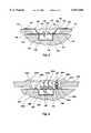
- FIG. 2is a top view of one die recess or bond site of FIG. 1 with a semiconductor die therein;
- FIG. 3is a side cross-sectional view of the present invention taken along line 3--3 of FIG. 1;
- FIGS. 4A and 4Bare a top and side plan view, respectively, of a single secondary clamp shown in FIGS. 1, 2 and 3;
- FIG. 5illustrates a "leads over chip” semiconductor configuration
- FIG. 6is a side view of another preferred embodiment of the invention.
- FIG. 7is a top view of yet another preferred embodiment of the invention.
- FIG. 8is a side view of yet another preferred embodiment of the invention illustrating a secondary clamp configuration.
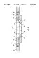
- FIG. 1illustrates an embodiment of the present invention designated as a dual clamp assembly 10.
- Assembly 10includes a generally rectangular primary clamp 12 including four mounting holes 14 at the four corners.
- the mounting holes 14are suitable for attaching the clamp 12 to matching holes on a mounting component (not shown) of a wire bonding apparatus.
- the clampis formed from a substantially rigid material, such as metal or the like, and is vertically reciprocably movable toward and away from an underlying heater block as known in the art.
- the clamp 12also includes four leaf spring members 50.
- the leaf spring members 50are pivotally mounted in recessed areas 52 in the clamp 12.
- the leaf spring members 50function to bias the assembly of the lead frame strip with attached die away from the clamp 12 upon the release of pressure of the clamp 12 from the lead frame strip.
- the primary clamp 12also includes two bond site windows 16, 18 extending completely through the clamp 12 from upper surface to lower surface.
- the bond site windows 16, 18are generally rectangular in shape and are spaced apart for proper indexing to match the spacing of the lead frames of the lead frame strip with attached die being wire bonded. Advantages of using multiple bond site windows are disclosed in U.S. Pat. No. 5,322,207 issued Jun. 21, 1994 to Fogal et al., which is hereby incorporated by reference.
- the bond site windows 16, 18are bordered by inner recesses 20, 22 defined at their inner peripheries by sloped walls extending downwardly to the window peripheries.
- a larger outer relief 24 or recessis formed around the two bond site windows 16, 18, encompassing inner recesses 20, 22.
- the bond site windows 16, 18are sized to allow access for a wire bonding tool head or capillary (not shown) to a plurality of bond pads 26 of semiconductor die 28 and to a plurality of lead fingers 30 of a lead frame 32.
- each bond site window 16, 18includes an opposing pair of secondary clamps 34.
- the secondary clamps 34are mounted to a distal end of a resilient plate 36 with a first set screw or bolt 38.
- the proximal end of each plate 36is attached to the primary clamp 12 with a second set screw or bolt 40.
- secondary clamps 34can be attached to the clamp 12 in any number of known configurations, including forming the clamps 34 with an integral resilient portion which is secured to the clamp 12 or forming (for example, as by machining) the secondary clamp 34 as an integrated, resilient appendage of the clamp 12.
- any number of secondary clamps 34can be used, consistent with the need for adequate clearances for wire bonding.
- clamps 34are configured with lateral cut-outs or recesses 35 to provide additional clearance for wire bonding tools. Such cut-outs may be of any suitable shape and size consistent with maintaining adequate torsional and bending rigidity of clamp 34.
- the semiconductor die 28has an LOC arrangement wherein the lead fingers 30 and buses 51 extend over the upper (active) semiconductor die 28.
- Buses 51are adhered to an alpha barrier or dielectric tape 46 (typically, as noted previously, KaptonTM tape) which is in turn adhered to the surface of the semiconductor die 28.
- Lead fingers 30free-float over the die surface but are not adhered thereto.
- the bond site window contact lip 44(FIG. 3) contacts the lead fingers 30 around the periphery of the semiconductor die 28.
- the opposing pair of secondary clamps 34extend toward the center of the semiconductor die 28, making contact therewith through buses 51 in this instance.
- a plurality of bond wires 48is then attached between the bond pads 26 of the semiconductor die 28 and the lead fingers 30 and buses 51.
- contact ends 42 of the secondary clamps 34 in their unbiased statepreferably extend slightly below a peripheral lead finger contact lip 44 of each bond site windows 16, 18 of the clamp 12.
- the secondary clamps 34may be formed from a substantially rigid, non-defornable material such as metal, high-temperature plastic, fiber composites, or the like.
- a preferred material for the secondary clamps 34is 440C stainless steel.
- FIGS. 4A and 4Billustrate an exemplary embodiment of the secondary clamp 34 as employed in FIG. 2.
- the secondary clampcomprises a mounting portion 54, an extension portion 56, and a contact portion 58.
- the mounting portion 54has a length 62 of about 0.105 inches, a width 64 of about 0.140 inches, a thickness 66 of about 0.035 inches, and a hole 60 disposed therethrough.
- the extension portion 56extends, angles, and tapers from the mounting portion 54 with a length 68 for cut-out 35 from the mounting portion 54 of about 0.125 inches, a tapered width 70 of about 0.070 inches, and an angle 74 of about 45 degrees.
- the contact portion 58extends, angles, and expands from the extension portion 56 with a length 72 of about 0.035 inches, an expanded width identical to mounting portion width 64 of about 0.140 inches, and an angle 76 from the extension portion angle 74 of an additional 15 degrees resulting in an angle of about 30 degrees from vertical.
- the additional contact portion angle 76begins at a first vertical distance 80 approximately 0.039 inches from the contact ends 42 or a second vertical distance 78 approximate 0.064 inches from the lower surface of the mounting portion 54.
- the contact portion thicknessis thinned proximate to the contact surface 42 with a radial recess 84 of a radius of approximately 0.025 inches.
- the radial recess 84begins at a third vertical distance 82 of approximately 0.073 inches from the lower surface of the mounting portion 54.
- clamp dimensions and configurationwill vary depending on the clamp 12, bond site size, semiconductor die 28 size and bond pad and lead frame element patterns.
- the primary considerationis that the configuration and resilient biasing force applied by the secondary clamps be effective in stabilizing the semiconductor die and the lead elements (or other lead frame elements) during the wire bonding process to eliminate the bouncing motion and/or movement of the semiconductor die or the lead elements.
- exemplary primary or workholder clamp 112 including a peripheral lip 144is positioned over a lead frame strip including a lead frame 132 aligned with a bond site window 116.
- Die 128, secured to the underside of lead frame 132is being wire bonded at its bond pads 126 to the lead fingers by wire bonds 148.
- secondary clamps 134comprise (by way of example) leaf springs which are secured at their proximal ends to the upper surface of clamp 112 by screws or bolts 140.
- secondary clamps 134In their unbiased modes, shown in broken lines, secondary clamps 134 extend below the lip 144 and so contact lead frame 132 first when clamp 112 is activated, thus imparting a spring force to lead fingers 130 as clamp 112 reaches the lower extent of its downward travel.
- These one-piece secondary clamps 134are formed by bending a leaf of spring steel or other suitable sheet metal downwardly at 150 and forming a presser foot 152 at the free or distal ends which contact the top of the lead fingers 130 outboard of die 128.
- presser foot 152is of arcuate (convex) configuration, but this is not a requirement.
- heater block 190may be recessed to accommodate the depth of die 128 and permit lead fingers 130 to remain planar when being clamped against heater block 190 by lip 144 and against the active surface of die 128 by clamps 134. This particular embodiment has utility for both LOC and conventional die attach assemblies.
- FIG. 7depicts yet another preferred embodiment of the invention, wherein a semiconductor die 228 with a central row of bond pads 226 is maintained in position by a primary clamp 212 having leaf spring secondary clamps 234 extending over bond site window 216.
- clamps 234may be maintained in position by set screws or bolts 240, as desired.
- Lead fingers 230 of a lead frame to which die 228 is securedare resiliently clamped against the active surface of die 228 through dielectric tape 246.
- Wire bonds 248extend between bond pads 226 and lead fingers 230, it is preferred, but not absolutely required, that clamp 212 include a lip on its underside to contact the lead fingers 230 outboard of the contact by secondary clamps 234.
- clamps 234may be of any suitable configuration. It should be further understood that one or more additional clamps 234', as shown in broken lines, may be included at an end of bond site window 216 if additional lead fingers 230 or buses (not shown) extend over die 228 at one or both ends of die 228.
- the present inventionis adapted to lead frame and die structures wherein both LOC and conventional lead fingers are employed together, as may be practiced with a dual lead frame construction wherein a first lead frame 332 with a die attach pad 333 and lead fingers 330 terminating at the die periphery is used with a second LOC lead frame 432 to provide additional lead fingers 430 and/or buses for additional electrical connections to die 328.
- a combination of secondary clamps 334a, 334b and 334cmay be employed to secure the lead fingers in position for wire bonding.
- a dual lead frame structureis also disclosed in U.S. Pat. No. 4,984,059 to Kubota et al.
- FIG. 8also illustrates three additional variations of a secondary clamp which may be employed in the present invention.
- Clamps 334a, 334b and 334care depicted secured to an exemplary primary clamp 312 and extending into bond site window 316.
- Clamp 334aincludes a rigid body 336a having a compliant insert (as, for example, an elastomer disc) 338a bonded to the distal end thereof, a presser foot 352a of metal or some other non-compliant material being secured to insert 338a to contact lead fingers 330.
- a compliant insertas, for example, an elastomer disc
- Clamp 334bis a multi-fingered resilient structure formed of sheet material such as spring steel and comprising a plurality of biasing fingers 336b, similar in configuration to secondary clamps 134, emanating from a common base secured to primary clamp 312 and of a number, size and arrangement to contact individual leads such as lead finger 430, buses, or other lead frame elements to be stabilized.
- Clamp 334cincludes a rigid body 336c with a downwardly-extending mandrel 337c having a vertically slidable tubular presser foot 352c biased downwardly thereon by a spring 338c, illustrated as a coil spring although a belleville spring or other spring configuration may be employed with equal effectiveness.
- rigid body 336cas illustrated, may comprise a flat metal plate having apertures formed therein for a plurality of mandrels 337c to be secured thereto in a pattern selected for contact of specific lead frame elements to be stabilized.
Landscapes
- Engineering & Computer Science (AREA)
- Computer Hardware Design (AREA)
- Microelectronics & Electronic Packaging (AREA)
- Power Engineering (AREA)
- Manufacturing & Machinery (AREA)
- Physics & Mathematics (AREA)
- Condensed Matter Physics & Semiconductors (AREA)
- General Physics & Mathematics (AREA)
- Mechanical Engineering (AREA)
- Wire Bonding (AREA)
Abstract
Description
Claims (17)
Priority Applications (1)
| Application Number | Priority Date | Filing Date | Title |
|---|---|---|---|
| US09/015,285US6047468A (en) | 1996-01-26 | 1998-01-29 | Lead finger clamp assembly and method of stabilizing lead frame elements |
Applications Claiming Priority (2)
| Application Number | Priority Date | Filing Date | Title |
|---|---|---|---|
| US08/592,058US5954842A (en) | 1996-01-26 | 1996-01-26 | Lead finger clamp assembly |
| US09/015,285US6047468A (en) | 1996-01-26 | 1998-01-29 | Lead finger clamp assembly and method of stabilizing lead frame elements |
Related Parent Applications (1)
| Application Number | Title | Priority Date | Filing Date |
|---|---|---|---|
| US08/592,058DivisionUS5954842A (en) | 1996-01-26 | 1996-01-26 | Lead finger clamp assembly |
Publications (1)
| Publication Number | Publication Date |
|---|---|
| US6047468Atrue US6047468A (en) | 2000-04-11 |
Family
ID=24369110
Family Applications (2)
| Application Number | Title | Priority Date | Filing Date |
|---|---|---|---|
| US08/592,058Expired - LifetimeUS5954842A (en) | 1996-01-26 | 1996-01-26 | Lead finger clamp assembly |
| US09/015,285Expired - LifetimeUS6047468A (en) | 1996-01-26 | 1998-01-29 | Lead finger clamp assembly and method of stabilizing lead frame elements |
Family Applications Before (1)
| Application Number | Title | Priority Date | Filing Date |
|---|---|---|---|
| US08/592,058Expired - LifetimeUS5954842A (en) | 1996-01-26 | 1996-01-26 | Lead finger clamp assembly |
Country Status (1)
| Country | Link |
|---|---|
| US (2) | US5954842A (en) |
Cited By (12)
| Publication number | Priority date | Publication date | Assignee | Title |
|---|---|---|---|---|
| US6227431B1 (en)* | 1996-01-26 | 2001-05-08 | Micron Technology, Inc. | Apparatus and method of clamping semiconductor devices using sliding finger supports |
| US6299049B1 (en)* | 1996-12-13 | 2001-10-09 | Micron Technology, Inc. | Device and method for clamping and wire-bonding the leads of a lead frame one set at a time |
| WO2002001612A3 (en)* | 2000-06-28 | 2002-06-06 | Advanced Micro Devices Inc | Mechanical clamper for heated substrates at die attach |
| US6657287B2 (en)* | 2002-05-03 | 2003-12-02 | Illinois Tool Works Inc. | Leadframe assembly |
| US20040026483A1 (en)* | 1996-06-17 | 2004-02-12 | Ball Michael B. | Methods for lead penetrating clamping system |
| US6804883B1 (en)* | 1999-06-25 | 2004-10-19 | Robert Bosch Gmbh | Method for producing a pressure sensor |
| US20050067462A1 (en)* | 2003-09-25 | 2005-03-31 | Unaxis International Trading Ltd. | Wire bonder with a downholder for pressing the fingers of a system carrier onto a heating plate |
| AU2003270420B2 (en)* | 2002-10-03 | 2007-03-15 | Frito-Lay North America, Inc. | Multi-layer flexible package with removable section |
| US20080237961A1 (en)* | 2007-03-30 | 2008-10-02 | Honda Motor Co., Ltd. | Pad for holding blank and die assembly therewith |
| WO2008076080A3 (en)* | 2006-12-21 | 2008-11-06 | Rokko Technology Pte Ltd | A clamping assembly |
| CN103996626A (en)* | 2013-02-17 | 2014-08-20 | 无锡华润上华科技有限公司 | Reworking method of lead hole |
| US11826861B1 (en)* | 2020-08-12 | 2023-11-28 | Sion Power Corporation | Joining systems, clamping fixtures, and related systems and methods |
Families Citing this family (19)
| Publication number | Priority date | Publication date | Assignee | Title |
|---|---|---|---|---|
| US6448169B1 (en)* | 1995-12-21 | 2002-09-10 | International Business Machines Corporation | Apparatus and method for use in manufacturing semiconductor devices |
| US6126062A (en) | 1998-04-02 | 2000-10-03 | Micron Technology, Inc. | Non-conductive and self-leveling leadframe clamp insert for wirebonding integrated circuits |
| US6634538B2 (en) | 1998-04-02 | 2003-10-21 | Micron Technology, Inc. | Non-conductive and self-leveling leadframe clamp insert for wirebonding integrated circuits |
| US6118175A (en)* | 1998-04-21 | 2000-09-12 | Motorola, Inc. | Wire bonding support structure and method for coupling a semiconductor chip to a leadframe |
| US6448107B1 (en)* | 2000-11-28 | 2002-09-10 | National Semiconductor Corporation | Pin indicator for leadless leadframe packages |
| US7048174B2 (en)* | 2003-08-25 | 2006-05-23 | The Boeing Company | Adaptable spring force clamping apparatus and methods |
| US9033328B2 (en)* | 2003-10-31 | 2015-05-19 | The Boeing Company | Reconfigurable clamping system |
| US7240820B2 (en)* | 2004-07-19 | 2007-07-10 | Asm Technology Singapore Pte Ltd. | Clamping device for processing electronic devices |
| US7748591B2 (en)* | 2004-12-14 | 2010-07-06 | The Boeing Company | Pressure foot clamp for friction stir welding machine |
| US20060237888A1 (en)* | 2005-04-22 | 2006-10-26 | The Boeing Company | Inflatable clamping systems and methods |
| CN101221916B (en)* | 2007-01-09 | 2010-05-19 | 日月光半导体制造股份有限公司 | Wire punching machine |
| US8752751B2 (en)* | 2012-07-13 | 2014-06-17 | Asm Technology Singapore Pte Ltd | Lead frame support plate and window clamp for wire bonding machines |
| US9997490B2 (en)* | 2015-03-20 | 2018-06-12 | Texas Instruments Incorporated | Window clamp |
| ITUA20162979A1 (en)* | 2016-04-28 | 2017-10-28 | Illinois Tool Works | HEADS FOR RIBBON PLATING WITH RIBBON PRESSURE LIMITS AND RIBBON BANDING SYSTEMS WITH HEADS FOR RIBBON BANDING WITH RIBBON PRESSURE LIMITS |
| ITUA20162983A1 (en) | 2016-04-28 | 2017-10-28 | Illinois Tool Works | HEADS FOR RIBBON PLATING HAVING INDEPENDENT BELT PRESSURE ADJUSTMENTS AND RIBBON BANDING SYSTEMS WITH HEADS FOR RIBBON BANDING WITH INDEPENDENT BELT PRESSURE ADJUSTMENT |
| ITUA20162977A1 (en) | 2016-04-28 | 2017-10-28 | Illinois Tool Works | TAPE FEEDERS FOR PLATING HAVING ADJUSTABLE RIBBON GUIDES AND RIBBON PLATING SYSTEMS WITH TAPE FEEDERS FOR PLATING HAVING ADJUSTABLE RIBBON GUIDES FOR THE RIBBON |
| ITUA20162975A1 (en) | 2016-04-28 | 2017-10-28 | Illinois Tool Works | TAPE FEEDERS FOR PLATING HAVING INDEPENDENT PRESSURE ROLLERS AND TAPE PLATING SYSTEMS WITH TAPE FEEDERS FOR PLATING HAVING INDEPENDENT PRESSURE ROLLERS |
| CN105880823B (en)* | 2016-05-30 | 2018-07-27 | 重庆航伟光电科技有限公司 | Optical fiber welding 4PIN heating platens |
| US10541223B2 (en)* | 2017-05-05 | 2020-01-21 | Kulicke And Soffa Industries, Inc. | Methods of operating a wire bonding machine to improve clamping of a substrate, and wire bonding machines |
Citations (26)
| Publication number | Priority date | Publication date | Assignee | Title |
|---|---|---|---|---|
| US3685137A (en)* | 1971-05-13 | 1972-08-22 | Rca Corp | Method for manufacturing wire bonded integrated circuit devices |
| US4030657A (en)* | 1972-12-26 | 1977-06-21 | Rca Corporation | Wire lead bonding tool |
| US4361261A (en)* | 1978-11-22 | 1982-11-30 | Kulicke & Soffa Industries, Inc. | Apparatus for wire bonding |
| US4434347A (en)* | 1981-08-19 | 1984-02-28 | Fairchild Camera And Instrument Corporation | Lead frame wire bonding by preheating |
| US4600138A (en)* | 1984-07-25 | 1986-07-15 | Hughes Aircraft Company | Bonding tool and clamp assembly and wire handling method |
| US4603803A (en)* | 1982-08-24 | 1986-08-05 | Asm Assembly Automation, Ltd. | Wire bonding apparatus |
| US4653681A (en)* | 1985-05-16 | 1987-03-31 | Kulicke And Soffa Industries, Inc. | Voice coil actuated fine wire clamp |
| US4765531A (en)* | 1987-05-14 | 1988-08-23 | Kulicke And Soffa Industries Inc. | Quick change work station apparatus for automatic wire bonders |
| US4778097A (en)* | 1986-12-04 | 1988-10-18 | Hauser John G | Ultrasonic wire bonding tool |
| US4800421A (en)* | 1981-09-01 | 1989-01-24 | Motorola, Inc. | Glass bonding means and method |
| US4821945A (en)* | 1987-07-01 | 1989-04-18 | International Business Machines | Single lead automatic clamping and bonding system |
| US4862245A (en)* | 1985-04-18 | 1989-08-29 | International Business Machines Corporation | Package semiconductor chip |
| US5035034A (en)* | 1990-07-16 | 1991-07-30 | Motorola, Inc. | Hold-down clamp with mult-fingered interchangeable insert for wire bonding semiconductor lead frames |
| US5062565A (en)* | 1990-07-13 | 1991-11-05 | Micron Technology, Inc. | Method for combining die attach and wirebond in the assembly of a semiconductor package |
| US5114066A (en)* | 1990-11-20 | 1992-05-19 | Texas Instruments Incorporated | Voice coil programmable wire tensioner |
| US5148959A (en)* | 1991-02-07 | 1992-09-22 | Tribotech | Wedge bonding tool |
| US5193733A (en)* | 1991-05-14 | 1993-03-16 | Goldstar Electron Co., Ltd. | Clamping device for inner leads of lead frame |
| US5217154A (en)* | 1989-06-13 | 1993-06-08 | Small Precision Tools, Inc. | Semiconductor bonding tool |
| US5307978A (en)* | 1991-11-15 | 1994-05-03 | Kulicke And Soffa Investments, Inc. | Smart indexing head for universal lead frame work station |
| US5322207A (en)* | 1993-05-03 | 1994-06-21 | Micron Semiconductor Inc. | Method and apparatus for wire bonding semiconductor dice to a leadframe |
| US5421503A (en)* | 1994-08-24 | 1995-06-06 | Kulicke And Soffa Investments, Inc. | Fine pitch capillary bonding tool |
| US5425491A (en)* | 1992-07-01 | 1995-06-20 | Sumitomo Electric Industries, Ltd. | Bonding tool, production and handling thereof |
| US5445306A (en)* | 1994-05-31 | 1995-08-29 | Motorola, Inc. | Wedge wire bonding tool tip |
| US5465899A (en)* | 1994-10-14 | 1995-11-14 | Texas Instruments Incorporated | Method and apparatus for fine pitch wire bonding using a shaved capillary |
| US5558267A (en)* | 1995-03-31 | 1996-09-24 | Texas Instruments Incorporated | Moat for die pad cavity in bond station heater block |
| US5611478A (en)* | 1996-03-11 | 1997-03-18 | National Semiconductor Corporation | Lead frame clamp for ultrasonic bonding |
- 1996
- 1996-01-26USUS08/592,058patent/US5954842A/ennot_activeExpired - Lifetime
- 1998
- 1998-01-29USUS09/015,285patent/US6047468A/ennot_activeExpired - Lifetime
Patent Citations (26)
| Publication number | Priority date | Publication date | Assignee | Title |
|---|---|---|---|---|
| US3685137A (en)* | 1971-05-13 | 1972-08-22 | Rca Corp | Method for manufacturing wire bonded integrated circuit devices |
| US4030657A (en)* | 1972-12-26 | 1977-06-21 | Rca Corporation | Wire lead bonding tool |
| US4361261A (en)* | 1978-11-22 | 1982-11-30 | Kulicke & Soffa Industries, Inc. | Apparatus for wire bonding |
| US4434347A (en)* | 1981-08-19 | 1984-02-28 | Fairchild Camera And Instrument Corporation | Lead frame wire bonding by preheating |
| US4800421A (en)* | 1981-09-01 | 1989-01-24 | Motorola, Inc. | Glass bonding means and method |
| US4603803A (en)* | 1982-08-24 | 1986-08-05 | Asm Assembly Automation, Ltd. | Wire bonding apparatus |
| US4600138A (en)* | 1984-07-25 | 1986-07-15 | Hughes Aircraft Company | Bonding tool and clamp assembly and wire handling method |
| US4862245A (en)* | 1985-04-18 | 1989-08-29 | International Business Machines Corporation | Package semiconductor chip |
| US4653681A (en)* | 1985-05-16 | 1987-03-31 | Kulicke And Soffa Industries, Inc. | Voice coil actuated fine wire clamp |
| US4778097A (en)* | 1986-12-04 | 1988-10-18 | Hauser John G | Ultrasonic wire bonding tool |
| US4765531A (en)* | 1987-05-14 | 1988-08-23 | Kulicke And Soffa Industries Inc. | Quick change work station apparatus for automatic wire bonders |
| US4821945A (en)* | 1987-07-01 | 1989-04-18 | International Business Machines | Single lead automatic clamping and bonding system |
| US5217154A (en)* | 1989-06-13 | 1993-06-08 | Small Precision Tools, Inc. | Semiconductor bonding tool |
| US5062565A (en)* | 1990-07-13 | 1991-11-05 | Micron Technology, Inc. | Method for combining die attach and wirebond in the assembly of a semiconductor package |
| US5035034A (en)* | 1990-07-16 | 1991-07-30 | Motorola, Inc. | Hold-down clamp with mult-fingered interchangeable insert for wire bonding semiconductor lead frames |
| US5114066A (en)* | 1990-11-20 | 1992-05-19 | Texas Instruments Incorporated | Voice coil programmable wire tensioner |
| US5148959A (en)* | 1991-02-07 | 1992-09-22 | Tribotech | Wedge bonding tool |
| US5193733A (en)* | 1991-05-14 | 1993-03-16 | Goldstar Electron Co., Ltd. | Clamping device for inner leads of lead frame |
| US5307978A (en)* | 1991-11-15 | 1994-05-03 | Kulicke And Soffa Investments, Inc. | Smart indexing head for universal lead frame work station |
| US5425491A (en)* | 1992-07-01 | 1995-06-20 | Sumitomo Electric Industries, Ltd. | Bonding tool, production and handling thereof |
| US5322207A (en)* | 1993-05-03 | 1994-06-21 | Micron Semiconductor Inc. | Method and apparatus for wire bonding semiconductor dice to a leadframe |
| US5445306A (en)* | 1994-05-31 | 1995-08-29 | Motorola, Inc. | Wedge wire bonding tool tip |
| US5421503A (en)* | 1994-08-24 | 1995-06-06 | Kulicke And Soffa Investments, Inc. | Fine pitch capillary bonding tool |
| US5465899A (en)* | 1994-10-14 | 1995-11-14 | Texas Instruments Incorporated | Method and apparatus for fine pitch wire bonding using a shaved capillary |
| US5558267A (en)* | 1995-03-31 | 1996-09-24 | Texas Instruments Incorporated | Moat for die pad cavity in bond station heater block |
| US5611478A (en)* | 1996-03-11 | 1997-03-18 | National Semiconductor Corporation | Lead frame clamp for ultrasonic bonding |
Cited By (31)
| Publication number | Priority date | Publication date | Assignee | Title |
|---|---|---|---|---|
| US6637636B2 (en) | 1996-01-26 | 2003-10-28 | Micron Technology, Inc. | Apparatus of clamping semiconductor devices using sliding finger supports |
| US6267287B1 (en)* | 1996-01-26 | 2001-07-31 | Micron Technology, Inc. | Apparatus and method of clamping semiconductor devices using sliding finger supports |
| US20060157532A1 (en)* | 1996-01-26 | 2006-07-20 | Ball Michael B | Apparatus of clamping semiconductor devices using sliding finger supports |
| US6981629B2 (en) | 1996-01-26 | 2006-01-03 | Micron Technology, Inc. | Apparatus of clamping semiconductor devices using sliding finger supports |
| US6227431B1 (en)* | 1996-01-26 | 2001-05-08 | Micron Technology, Inc. | Apparatus and method of clamping semiconductor devices using sliding finger supports |
| US6715659B2 (en) | 1996-01-26 | 2004-04-06 | Micron Technology, Inc. | Apparatus for clamping semiconductor devices using sliding finger supports |
| US6484922B2 (en) | 1996-01-26 | 2002-11-26 | Micron Technology, Inc. | Apparatus and method of clamping semiconductor devices using sliding finger supports |
| US7131568B2 (en) | 1996-06-17 | 2006-11-07 | Micron Technology, Inc. | Methods for lead penetrating clamping system |
| US20040026483A1 (en)* | 1996-06-17 | 2004-02-12 | Ball Michael B. | Methods for lead penetrating clamping system |
| US6786387B2 (en) | 1996-12-13 | 2004-09-07 | Micron Technology, Inc. | Method for clamping and wire-bonding the leads of a lead frame one set at a time |
| US6886734B2 (en) | 1996-12-13 | 2005-05-03 | Micron Technology, Inc. | Device and method for clamping and wire-bonding the leads of a lead frame one set at a time |
| US6299049B1 (en)* | 1996-12-13 | 2001-10-09 | Micron Technology, Inc. | Device and method for clamping and wire-bonding the leads of a lead frame one set at a time |
| US20020179691A1 (en)* | 1996-12-13 | 2002-12-05 | Ball Michael B. | Device and method for clamping and wire-bonding the leads of a lead frame one set at a time |
| US6478211B2 (en) | 1996-12-13 | 2002-11-12 | Micron Technology, Inc. | Device and method for clamping and wire-bonding the leads of a lead frame one set at a time |
| US6467672B2 (en) | 1996-12-13 | 2002-10-22 | Micron Technology, Inc. | Methods for clamping and wire-bonding the leads of a lead frame one set at a time |
| US6334566B1 (en) | 1996-12-13 | 2002-01-01 | Micron Technology | Device and method for clamping and wire-bonding the leads of a lead frame one set at a time |
| US6804883B1 (en)* | 1999-06-25 | 2004-10-19 | Robert Bosch Gmbh | Method for producing a pressure sensor |
| WO2002001612A3 (en)* | 2000-06-28 | 2002-06-06 | Advanced Micro Devices Inc | Mechanical clamper for heated substrates at die attach |
| US6547121B2 (en)* | 2000-06-28 | 2003-04-15 | Advanced Micro Devices, Inc. | Mechanical clamper for heated substrates at die attach |
| US6657287B2 (en)* | 2002-05-03 | 2003-12-02 | Illinois Tool Works Inc. | Leadframe assembly |
| AU2003270420B8 (en)* | 2002-10-03 | 2007-04-05 | Frito-Lay North America, Inc. | Multi-layer flexible package with removable section |
| AU2003270420B2 (en)* | 2002-10-03 | 2007-03-15 | Frito-Lay North America, Inc. | Multi-layer flexible package with removable section |
| US7134589B2 (en)* | 2003-09-25 | 2006-11-14 | Unaxis International Trading Ltd. | Wire bonder with a downholder for pressing the fingers of a system carrier onto a heating plate |
| US20050067462A1 (en)* | 2003-09-25 | 2005-03-31 | Unaxis International Trading Ltd. | Wire bonder with a downholder for pressing the fingers of a system carrier onto a heating plate |
| WO2008076080A3 (en)* | 2006-12-21 | 2008-11-06 | Rokko Technology Pte Ltd | A clamping assembly |
| US20100096735A1 (en)* | 2006-12-21 | 2010-04-22 | Rokko Technology Pte Ltd. | Clamping assembly |
| CN101652859B (en)* | 2006-12-21 | 2011-07-06 | 洛科科技有限公司 | clamping components |
| US20080237961A1 (en)* | 2007-03-30 | 2008-10-02 | Honda Motor Co., Ltd. | Pad for holding blank and die assembly therewith |
| CN103996626A (en)* | 2013-02-17 | 2014-08-20 | 无锡华润上华科技有限公司 | Reworking method of lead hole |
| CN103996626B (en)* | 2013-02-17 | 2017-07-07 | 无锡华润上华科技有限公司 | The reworking method of fairlead |
| US11826861B1 (en)* | 2020-08-12 | 2023-11-28 | Sion Power Corporation | Joining systems, clamping fixtures, and related systems and methods |
Also Published As
| Publication number | Publication date |
|---|---|
| US5954842A (en) | 1999-09-21 |
Similar Documents
| Publication | Publication Date | Title |
|---|---|---|
| US6047468A (en) | Lead finger clamp assembly and method of stabilizing lead frame elements | |
| US5611478A (en) | Lead frame clamp for ultrasonic bonding | |
| US5933327A (en) | Wire bond attachment of a integrated circuit package to a heat sink | |
| US5976964A (en) | Method of improving interconnect of semiconductor device by utilizing a flattened ball bond | |
| US5793108A (en) | Semiconductor integrated circuit having a plurality of semiconductor chips | |
| US5666003A (en) | Packaged semiconductor device incorporating heat sink plate | |
| US6000599A (en) | Bondhead lead clamp apparatus and method | |
| KR930020649A (en) | Lead frame, semiconductor integrated circuit device using same, and manufacturing method thereof | |
| US5558267A (en) | Moat for die pad cavity in bond station heater block | |
| US6105846A (en) | Non-conductive and self-leveling leadframe clamp insert for wirebonding integrated circuits | |
| KR100473464B1 (en) | A semiconductor device | |
| US6634538B2 (en) | Non-conductive and self-leveling leadframe clamp insert for wirebonding integrated circuits | |
| KR200159223Y1 (en) | Inner lead clamp structure of wire bonding apparatus | |
| JP2000323522A (en) | Vertical movement device | |
| US6172318B1 (en) | Base for wire bond checking | |
| JPH0747868Y2 (en) | Lead frame holder in chip bonding or wire bonding process | |
| US7181835B2 (en) | Universal clamping mechanism | |
| KR100321149B1 (en) | chip size package | |
| JPS5930535Y2 (en) | semiconductor equipment | |
| KR100799202B1 (en) | Wire bonder head | |
| JPH0595074A (en) | Semiconductor device | |
| JPH1012655A (en) | Heater plate for wire bonder | |
| JPH0758143A (en) | Wire bonding equipment | |
| JPH01231334A (en) | Wire bonding method | |
| JPH04267545A (en) | Plastic molded type semiconductor device |
Legal Events
| Date | Code | Title | Description |
|---|---|---|---|
| STCF | Information on status: patent grant | Free format text:PATENTED CASE | |
| FPAY | Fee payment | Year of fee payment:4 | |
| FPAY | Fee payment | Year of fee payment:8 | |
| FEPP | Fee payment procedure | Free format text:PAYOR NUMBER ASSIGNED (ORIGINAL EVENT CODE: ASPN); ENTITY STATUS OF PATENT OWNER: LARGE ENTITY | |
| FPAY | Fee payment | Year of fee payment:12 | |
| AS | Assignment | Owner name:U.S. BANK NATIONAL ASSOCIATION, AS COLLATERAL AGENT, CALIFORNIA Free format text:SECURITY INTEREST;ASSIGNOR:MICRON TECHNOLOGY, INC.;REEL/FRAME:038669/0001 Effective date:20160426 Owner name:U.S. BANK NATIONAL ASSOCIATION, AS COLLATERAL AGEN Free format text:SECURITY INTEREST;ASSIGNOR:MICRON TECHNOLOGY, INC.;REEL/FRAME:038669/0001 Effective date:20160426 | |
| AS | Assignment | Owner name:MORGAN STANLEY SENIOR FUNDING, INC., AS COLLATERAL AGENT, MARYLAND Free format text:PATENT SECURITY AGREEMENT;ASSIGNOR:MICRON TECHNOLOGY, INC.;REEL/FRAME:038954/0001 Effective date:20160426 Owner name:MORGAN STANLEY SENIOR FUNDING, INC., AS COLLATERAL Free format text:PATENT SECURITY AGREEMENT;ASSIGNOR:MICRON TECHNOLOGY, INC.;REEL/FRAME:038954/0001 Effective date:20160426 | |
| AS | Assignment | Owner name:U.S. BANK NATIONAL ASSOCIATION, AS COLLATERAL AGENT, CALIFORNIA Free format text:CORRECTIVE ASSIGNMENT TO CORRECT THE REPLACE ERRONEOUSLY FILED PATENT #7358718 WITH THE CORRECT PATENT #7358178 PREVIOUSLY RECORDED ON REEL 038669 FRAME 0001. ASSIGNOR(S) HEREBY CONFIRMS THE SECURITY INTEREST;ASSIGNOR:MICRON TECHNOLOGY, INC.;REEL/FRAME:043079/0001 Effective date:20160426 Owner name:U.S. BANK NATIONAL ASSOCIATION, AS COLLATERAL AGEN Free format text:CORRECTIVE ASSIGNMENT TO CORRECT THE REPLACE ERRONEOUSLY FILED PATENT #7358718 WITH THE CORRECT PATENT #7358178 PREVIOUSLY RECORDED ON REEL 038669 FRAME 0001. ASSIGNOR(S) HEREBY CONFIRMS THE SECURITY INTEREST;ASSIGNOR:MICRON TECHNOLOGY, INC.;REEL/FRAME:043079/0001 Effective date:20160426 | |
| AS | Assignment | Owner name:MICRON TECHNOLOGY, INC., IDAHO Free format text:RELEASE BY SECURED PARTY;ASSIGNOR:U.S. BANK NATIONAL ASSOCIATION, AS COLLATERAL AGENT;REEL/FRAME:047243/0001 Effective date:20180629 | |
| AS | Assignment | Owner name:MICRON TECHNOLOGY, INC., IDAHO Free format text:RELEASE BY SECURED PARTY;ASSIGNOR:MORGAN STANLEY SENIOR FUNDING, INC., AS COLLATERAL AGENT;REEL/FRAME:050937/0001 Effective date:20190731 |