US6046982A - Method and apparatus for reducing data loss in data transfer devices - Google Patents
Method and apparatus for reducing data loss in data transfer devicesDownload PDFInfo
- Publication number
- US6046982A US6046982AUS08/819,273US81927397AUS6046982AUS 6046982 AUS6046982 AUS 6046982AUS 81927397 AUS81927397 AUS 81927397AUS 6046982 AUS6046982 AUS 6046982A
- Authority
- US
- United States
- Prior art keywords
- memory
- input
- data
- cell
- bandwidth
- Prior art date
- Legal status (The legal status is an assumption and is not a legal conclusion. Google has not performed a legal analysis and makes no representation as to the accuracy of the status listed.)
- Expired - Lifetime
Links
- 238000012546transferMethods0.000titleclaimsabstractdescription65
- 238000000034methodMethods0.000titleclaimsabstractdescription55
- 230000015654memoryEffects0.000claimsabstractdescription197
- 239000000872bufferSubstances0.000claimsabstractdescription69
- 230000008859changeEffects0.000claimsabstractdescription4
- 238000012544monitoring processMethods0.000claimsabstractdescription4
- 238000004891communicationMethods0.000claimsdescription17
- 238000001514detection methodMethods0.000claimsdescription15
- 230000006727cell lossEffects0.000claimsdescription13
- 230000003247decreasing effectEffects0.000claimsdescription4
- 238000012986modificationMethods0.000claimsdescription2
- 230000004048modificationEffects0.000claimsdescription2
- 238000004590computer programMethods0.000claims5
- 230000008878couplingEffects0.000claims1
- 238000010168coupling processMethods0.000claims1
- 238000005859coupling reactionMethods0.000claims1
- 230000008569processEffects0.000abstractdescription34
- 230000000694effectsEffects0.000abstractdescription2
- 210000004027cellAnatomy0.000description181
- 241001522296Erithacus rubeculaSpecies0.000description9
- 238000013461designMethods0.000description9
- 238000012545processingMethods0.000description9
- 238000010586diagramMethods0.000description5
- 210000003719b-lymphocyteAnatomy0.000description4
- 230000032258transportEffects0.000description4
- 230000009471actionEffects0.000description2
- 230000005540biological transmissionEffects0.000description2
- 230000015572biosynthetic processEffects0.000description2
- 230000006870functionEffects0.000description2
- 230000006984memory degenerationEffects0.000description2
- 230000004044responseEffects0.000description2
- 238000003786synthesis reactionMethods0.000description2
- 238000010420art techniqueMethods0.000description1
- 230000008901benefitEffects0.000description1
- 238000010276constructionMethods0.000description1
- 230000009977dual effectEffects0.000description1
- 238000005516engineering processMethods0.000description1
- RGNPBRKPHBKNKX-UHFFFAOYSA-NhexaflumuronChemical compoundC1=C(Cl)C(OC(F)(F)C(F)F)=C(Cl)C=C1NC(=O)NC(=O)C1=C(F)C=CC=C1FRGNPBRKPHBKNKX-UHFFFAOYSA-N0.000description1
- 230000011664signalingEffects0.000description1
- 230000001052transient effectEffects0.000description1
Images


Classifications
- H—ELECTRICITY
- H04—ELECTRIC COMMUNICATION TECHNIQUE
- H04L—TRANSMISSION OF DIGITAL INFORMATION, e.g. TELEGRAPHIC COMMUNICATION
- H04L49/00—Packet switching elements
- H04L49/10—Packet switching elements characterised by the switching fabric construction
- H04L49/103—Packet switching elements characterised by the switching fabric construction using a shared central buffer; using a shared memory
- H—ELECTRICITY
- H04—ELECTRIC COMMUNICATION TECHNIQUE
- H04L—TRANSMISSION OF DIGITAL INFORMATION, e.g. TELEGRAPHIC COMMUNICATION
- H04L12/00—Data switching networks
- H04L12/54—Store-and-forward switching systems
- H04L12/56—Packet switching systems
- H04L12/5601—Transfer mode dependent, e.g. ATM
- H04L12/5602—Bandwidth control in ATM Networks, e.g. leaky bucket
- H—ELECTRICITY
- H04—ELECTRIC COMMUNICATION TECHNIQUE
- H04L—TRANSMISSION OF DIGITAL INFORMATION, e.g. TELEGRAPHIC COMMUNICATION
- H04L49/00—Packet switching elements
- H04L49/10—Packet switching elements characterised by the switching fabric construction
- H04L49/104—Asynchronous transfer mode [ATM] switching fabrics
- H04L49/105—ATM switching elements
- H04L49/108—ATM switching elements using shared central buffer
- H—ELECTRICITY
- H04—ELECTRIC COMMUNICATION TECHNIQUE
- H04L—TRANSMISSION OF DIGITAL INFORMATION, e.g. TELEGRAPHIC COMMUNICATION
- H04L49/00—Packet switching elements
- H04L49/30—Peripheral units, e.g. input or output ports
- H04L49/3081—ATM peripheral units, e.g. policing, insertion or extraction
- H—ELECTRICITY
- H04—ELECTRIC COMMUNICATION TECHNIQUE
- H04L—TRANSMISSION OF DIGITAL INFORMATION, e.g. TELEGRAPHIC COMMUNICATION
- H04L49/00—Packet switching elements
- H04L49/50—Overload detection or protection within a single switching element
- H04L49/501—Overload detection
- H04L49/503—Policing
- H—ELECTRICITY
- H04—ELECTRIC COMMUNICATION TECHNIQUE
- H04L—TRANSMISSION OF DIGITAL INFORMATION, e.g. TELEGRAPHIC COMMUNICATION
- H04L12/00—Data switching networks
- H04L12/54—Store-and-forward switching systems
- H04L12/56—Packet switching systems
- H04L12/5601—Transfer mode dependent, e.g. ATM
- H04L2012/5672—Multiplexing, e.g. coding, scrambling
- H—ELECTRICITY
- H04—ELECTRIC COMMUNICATION TECHNIQUE
- H04L—TRANSMISSION OF DIGITAL INFORMATION, e.g. TELEGRAPHIC COMMUNICATION
- H04L12/00—Data switching networks
- H04L12/54—Store-and-forward switching systems
- H04L12/56—Packet switching systems
- H04L12/5601—Transfer mode dependent, e.g. ATM
- H04L2012/5678—Traffic aspects, e.g. arbitration, load balancing, smoothing, buffer management
- H04L2012/5679—Arbitration or scheduling
- H—ELECTRICITY
- H04—ELECTRIC COMMUNICATION TECHNIQUE
- H04L—TRANSMISSION OF DIGITAL INFORMATION, e.g. TELEGRAPHIC COMMUNICATION
- H04L49/00—Packet switching elements
- H04L49/30—Peripheral units, e.g. input or output ports
Definitions
- This inventionrelates, in general, to data transfer devices and specifically to methods and apparatus useful in shared memory devices for reducing packet or cell loss in store and forward operations.
- Computer hardwareis becoming increasingly distributed and remote, resulting in networks of computers for solving problems in concert rather than as stand-alone systems. Although such distributed "services" networks generally facilitate problem-solving, they also increase the need for flexibility and functionality in software programs operating on the computers.
- An example of a distributed services computer networkis a "client-server" system which comprises a collection of client nodes, e.g., workstations or personal computers, that communicate over a network with various server nodes. Each node is connected to the transmission medium at an address which uniquely identifies the node and which is used to route data from one node to another.
- the server nodesare typically computers having hardware and software elements that provide a sophisticated set of services, or operations, for use by the client nodes to increase the efficiency of their own operations.
- networksmay be employed in the client-server system which are connected by one or more communication links that may be interconnected to other communication links and nodes within the network through bridges or routers.
- Nodes coupled to the networktypically communicate by exchanging messages which comprise discrete "packets" of data. These packets can be transported over the network with one of a variety of transport techniques.
- ATMAsynchronous transfer mode
- data packets to be transportedare first broken up into ATM cells, transmitted, and then reassembled at a destination.
- ATM cellsare 53 bytes long. Each cell consists of a 5-byte header and a 48-byte information field. The header of an ATM cell contains the information used to transport the cell from one node to the next over a route which has been previously established by means of a separate signaling channel. User data is contained in the remaining 48 bytes.
- the preestablished route over which the cells passexists only as sets of routing tables held in each network node or switch, which tables determine the physical connection of the communication links. These routing tables are based on a virtual circuit identifier (VCI) code and a virtual path identifier (VPI) code contained in header of each ATM cell.
- VCIvirtual circuit identifier
- VPNvirtual path identifier
- a cellis passed through each ATM switch and over each communication link via the pre-established route, but the route is considered "virtual" since the route carrying the cell is dedicated to it only while the cell traverses it.
- the physical facilitiesare shared among various routes. For example, two cells that are ultimately headed for different destinations may be sequentially carried for part of their journey over the same physical wire.
- a typical ATM switchacts as a cell relay.
- the input side of the switchcontains a first in-first out buffer (FIFO) queue connected to the media input port.
- Cellsarrive from the incoming communication link at an input data rate and are entered into one end of the buffer.
- the switching processinvolves examining each cell in turn at the other end of the buffer and determining from the VCI/VPI codes in the cell header which output line should be used. The cell is then added to a FIFO buffer queue for that output line which holds cells waiting to be transmitted on the associated outgoing communication link.
- FIFOfirst in-first out buffer
- Switch congestionoccurs when either the input or output FIFO buffers fill to a predetermined level. If the congestion becomes severe enough, the buffers may become completely full, in which case there is no space for incoming packets or cells to be stored and the packets or cells are lost.
- the cell loss problemis exacerbated because the flow of cells on the network is generally "bursty" in nature rather than steady.
- Most network applicationsoperate independently of each other and generate a "burst" of data in response to some event such as a certain time of day or a user action.
- An example of a user action which generates network trafficis the generation of a "copy command" which starts a process that results in a data file being transported across the network.
- Such a copy commandmight generate one or many packets on a LAN which are eventually switched onto a backbone which connects to another LAN. For example, a typical Ethernet LAN packet of 1000 bytes would appear on the ATM backbone as a 60 microsecond burst of roughly 21 ATM cells.
- burstsare widely separated from the previous and next burst of cells because the bursts are caused by independent events. Consequently, the average data rate, which is often calculated over the period of many milliseconds, can include much idle time and be much less that the peak data rate during a burst.
- network devicesare designed to accommodate the peak data rate of common traffic patterns.
- a common prior art techniqueis to design network equipment to be able to handle the expected peak data rate for unlimited time periods. This technique is effective but results in equipment which has expensive capacity that is not needed most of the time.
- a typical switch designfor example an ATM network, uses a shared memory switch.
- received cells at each of the input portsare demultiplexed (if necessary) and put onto queues located in a common cell memory. These queues take the form of linked lists in the common memory. Buffer memory is effectively allocated from the common memory pool as it is needed so that the output buffers which are represented by the queues can be of different lengths.
- the switchreceives cells from a media input port and stores them in memory. Concurrently, the switch reads cells from the memory and forwards them to an output port for transmission on a medium.
- the memoryis sized to buffer a sufficient number of cells in order to handle the bursty nature of the cell flow in the network.
- Such a memorytypically has an input bandwidth which indicates the rate at which cells are stored and an output bandwidth which indicates the rate at which cells are forwarded.
- the overall memory throughputis generally the average of the input and output bandwidths.
- Dual ported memoriesare commonly used for the common memory pool so that one memory port is used to store cells in the memory while the other memory port is used to forward cells out of the memory.
- a dual-port memory designrequires arbitration between the input and output ports because the physical memory element cannot be simultaneously written and read. The cells are transferred much more quickly inside the switch than their arrival rate at the switch. Since each cell that arrives must also be forwarded, the shared memory element typically uses a round robin arbitration scheme between the input and output ports. In a traditional shared memory switch, round robin arbitration among the input and output ports results in a sequence of operations alternating between memory-write (cell store) and memory-read (cell forward). In addition, a round robin arbitration scheme is also used between the various input or output ports since only one input port can store at once and only one output port can read at once.
- a small first in-first out (FIFO) bufferis provided at each input port to the switch.
- the size of each input FIFOis normally very small, since the cost/bit of the FIFO buffer memories is high when compared to the cost/bit of the main shared memory.
- Cells that arrive from one input portare entered into one end of the FIFO input buffer connected to that port.
- the switching processinvolves examining each cell, in turn, at the other end of the FIFO input buffer and determining from the routing codes in the cell header which output port should be used. The cell is then added to a buffer queue in the main shared memory for that output port.
- the input bandwidth of a data transfer deviceis increased, and the output bandwidth of the device is decreased by altering the conventional memory arbitration method.
- the input data rateis monitored and when the input data rate exceeds the maximum average throughput of the memory, the outcome of the memory arbitration is changed so that the data transfer cycle consists of two stores (memory write operations) instead of one store and one forward (memory read operation.)
- memory output operationsare stolen to increase the number of memory input operations when the input load exceeds that of the maximum average memory throughput.
- the input loadis detected by monitoring the input port FIFO buffers for the presence of data cells waiting for storage. Based on the results of the FIFO monitoring and the outcome of the current port arbitration cycle, a decision is made on the following port arbitration cycle whether to change the normal memory arbitration pattern.
- the input portsare assigned to two separate controllers and a single arbitration circuit is used to arbitrate between ports on both of the controllers.
- FIG. 1is a block schematic diagram of an ATM switching network illustrating the connection of switches
- FIG. 2is a more detailed block diagram of an ATM switch illustrating the input FIFOs, the arbitration circuitry and the shared memory.
- FIG. 3is a more detailed block diagram of an ATM switch illustrating the input FIFOs, the arbitration circuitry and the shared memory in a preferred embodiment.
- FIG. 4is a flowchart illustrating the port arbitration processing in accordance with the principles of the present invention.
- FIG. 5is a schematic diagram illustrating incoming cell processing in one example input situation.
- FIG. 6is a schematic diagram illustrating incoming cell processing in a second example input situation.
- FIG. 1illustrates, in very generalized form, an ATM switched network involving five stations 100, 106, 124, 130 and 134, respectively.
- each station 100, 106, 124, 130 and 134contains software which breaks the data into cells and affixes an appropriate header indicating how each cell should be routed through the network.
- Each stationalso contains software which receives cells and reassembles the packets into the completed data packets.
- an ATM switching network utilizing cellsis illustratively shown and described in the examples which follow, the principles of the present invention can also be used with other types of data packet networks and packet switches. The use of an ATM switch is in no way intended to imply that the invention is limited to such switches.
- Stations 100 and 106are connected to ATM cell switch 114, and stations 124 and 130 are connected to switch 112. Similarly, station 134 is connected to switch 122.
- An arbitration method and apparatus constructed in accordance with the principles of the present inventioncan run in switches 112, 114 and 122.
- Switches 112, 114 and 122route cells between the stations 100, 106, 124, 130 and 134 and control access to the network. For example, station 100 may send cells over media line 104 to media input port 102 of switch 114.
- Switch 114may route cells to a destination station, for example station 124, based on the information in each cell header. To do this, cells are first switched by switch 114 onto output line 115, via output port 110 to input port 116 of switch 112.
- Switch 112then routes the cells, via output port 126 to station 124.
- station 106can be connected to station 134 by means of input port 108 on switch 114, output port 118, communication line 121, input port 120 of switch 122 and output port 132.
- input port 108 on switch 114output port 118
- communication line 121input port 120 of switch 122
- input port 120 of switch 122output port 132
- switches 112, 114 and 122typically, each switch would have many input and output ports, for example eight input ports and eight output ports.
- Each ATM switchacts as a cell relay.
- the input side of the switchcontains a first in-first out (FIFO) buffer queue connected to each of the media input ports 102 and 108.
- Cellsarrive from the incoming communication link 104 and are entered into one end of the buffer.
- the switching processinvolves examining each cell, in turn, at the other end of the buffer and determining from the routing codes in the cell header which output line should be used.
- the cellis then added to a FIFO buffer queue for that output line which holds cells waiting to be transmitted on the associated outgoing communication links 115 or 121. It is important that the switching process operate efficiently because data packets can arrive at closely spaced intervals. Switch congestion occurs when either the input or output FIFO buffers fill to a predetermined level. If the congestion becomes severe enough the buffers may become completely full, in which case there is no space for incoming packets to be stored and the packets are lost.
- FIFOfirst in-first out
- a conventional data transfer cycleinvolves two steps, one store operation followed by one forward operation.
- the store operationis a 53-byte memory write operation and the forward operation is a 53-byte memory read operation.
- the arbiteruses a store/store cycle instead of a store/forward cycle.
- the present inventionmodifies the arbitration to temporarily increase the number of input operations while correspondingly decreasing the number of output operations.
- FIG. 2illustrates, in more detail, the construction, in accordance with the principles of the invention, of an ATM switch, such as switches 112, 114 or 122.
- Cellsarrive on inputs 200-214 which are connected to input FIFOs 216-230, respectively.
- the outputs of FlFOs 216-230are, in turn, connected to multiplexer 232 which is controlled by an arbitration circuit 236.
- arbitration circuit 236receives inputs from the FIFOs 216-230 in order to select the output of one of FlFOs 216-230 for forwarding.
- the output of multiplexer 232is connected to the common shared memory bus 234.
- Cells on the common bus 234may be stored in an appropriate queue in the shared buffer memory 238 under control of memory control 240.
- Memory control 240can also read cells out of memory 238 and transmit them, via the common bus 234 to output ports, not shown, which would be coupled via terminal 242.
- a memory store/forward arbitration processis performed by arbitration circuit 236 to decide whether a write or a read will be performed at a given time.
- Memory arbitrationinvolves selecting from two processes for each memory element, an input process which stores a cell in the shared memory 238 and an output process which reads a cell from the shared memory 238.
- round-robin arbitrationoccurs separately for memory input and output processes and, in accordance with the principles of the present invention, the memory input process is given priority which effectively allows short bursts wherein the entire memory system bandwidth is allocated to the input process.
- the output bandwidthmust equal or exceed input bandwidth for the central shared memory, or cell loss will occur.
- a peak in the aggregate input data rateis detected in the input FIFOs 216-230 normally present for each port. This detection is performed by arbitration circuit 236.
- an input portneeds to store a minimum of three cells in a FIFO, labeled (for purposes of discussion) cells A, B and C.
- the A cellis a cell which will be written to memory 238 if the associated port wins the input port arbitration cycle.
- the B cellis a cell which arrived after the A cell and must be buffered if the A cell has not been written.
- the B portion of the each FIFOmight be absent or might hold one or more cells.
- the C portion of the FIFOholds a cell is currently still arriving from the serial media, so that the presence of this cell is detected only after it completely arrives.
- the throughput of the switchwould be 800 Mb/s.
- a common port speedis sTS3c SONET, or 155 Mb/s. Therefore, if the switch has eight input ports, and all ports are inputting data simultaneously, the aggregate input data rate is 1.2 Gb/s, which exceeds the memory throughput.
- the memory controllercan store and forward slightly more than five cells in the time it takes one 53 byte cell to arrive at a port. With eight ports, eight cells could arrive at once and occupy the eight A FIFO locations.
- the arbitration circuit 236, or "arbiter”modifies the store/forward data transfer cycle to be store/store data transfer cycle when the peak in the input data rate is detected.
- the arbiterWhen a cell is detected in any B FIFO location, priority is given to the input process, performing round-robin storing of all occupied A FIFO locations until the B FIFO location empties. If full memory bandwidth is used to store cells, the arbiter can empty ten of the A FIFO locations before another cell can arrive. Thus, for any arrival pattern, it is guaranteed that cells in B FIFO locations will be moved to A FIFO locations in time to prevent cell loss.
- An alternative implementationmay have a FIFO with more stages, thereby allowing more than one cell to be stored of type B, and bandwidth sharing can be invoked only after a predetermined number of cells arrive.
- FIG. 3illustrates a preferred embodiment of a cell switch constructed in accordance with the principles of the invention.
- the switchcomprises two input controllers 300 and 302, which are designated as controller 1, 300, and controller 2, 302.
- controller 1, 300and controller 2 302.
- the use of two controllersis not necessary for the principles of the present invention, but facilitates overcoming certain technology limitations of the hardware used to implement the described embodiment.
- the output of controller 300is connected to a speed matching FIFO 304.
- the output of controller 302is connected to speed matching FIFO 306.
- Speed matching FIFOs 304 and 306are illustrated for descriptive purposes only, and their function can be incorporated into controllers 300 and 302 by using the controller FIFOs.
- arbitration circuit 307receives inputs from the controller 1, 300, and controller 2, 302, in order to select the output of one controller for storing.
- the output of multiplexer 308is connected to the common shared memory bus 310.
- Cells on the common bus 310may be stored in an appropriate queue in the shared buffer memory 312 under control of memory control 314.
- Memory control 314can also read cells out of memory 312 and transmit them, via the common bus 310 to output ports, not shown, that would be coupled at terminal 318.
- Another speed matching FIFO 316is used to match the internal memory speed to the output port speed.
- a memory (store/forward) arbitration processmust be performed by arbitration circuit 307 to decide whether a write or a read will be performed at any given time.
- Memory arbitrationincludes two processes, an input process which stores a cell in the shared memory 312 and an output process which reads a cell from the shared memory 312. More particularly, a standard data transfer cycle is a store/forward cycle, and involves two steps, one store (memory write) operation followed by one forward (memory read) operation.
- the memory arbitration of circuit 307selects a store/store cycle instead of a store/forward cycle. This effectively allows short bursts wherein the entire memory system bandwidth is allocated to the input process.
- the switchhas an aggregate input data rate which may be from a single port or, more commonly, from a plurality of parallel ports, as in the embodiments of FIGS. 2 and 3.
- Input congestionis caused when the aggregate input data rate exceeds the memory throughput of the device.
- input congestionis detected in the input FIFO's connected to each input port.
- the B cell portion of the input FIFOshas been eliminated in order to further reduce costs.
- Arbitration and congestion detection functionsmay be based on the same cell, although this causes the store/store cycle to be needed more often than in the first described embodiment. In this case, the combined locations are labeled "A" for descriptive purposes.
- Congestionis detected by a technique which uses flags to pass information from arbitration cycle to arbitration cycle. Consequently, the input port FIFOs need to store a minimum of two cells, labeled A and C in FIFOs 320-326 and 336-342.
- the A locationsare examined to decide which input port will write to shared memory 312 during the store portion of the memory arbitration cycle.
- the A portion of each input FIFOalso contains the cell which will be written to the shared memory 312 if the associated port wins the arbitration.
- the C portion of the FIFOholds a cell which may be currently still arriving from the serial media, so that the presence of this cell is detected only after it completely arrives.
- decisions to schedule cell storing and forwardingare based on machine slot time of the memory control 314 instead of a cycle of length equal to the minimum time between arrival of cells.
- a machine slot timeis the time needed to perform a data transfer cycle, i.e., a cell store and a cell forward or two cell stores. If each input port is a conventional 155 Mb/s serial port and the memory throughput (during normal store/forward operation) is 800 Mb/s, there will be approximately five machine slot times between each possible cell arrival. If the switch has eight ports, eight cells may arrive in the time required for roughly 5 cells to be written and input congestion can occur with the normal store/forward memory arbitration cycle.
- the normal store/forward data transfer cycle(which has a input bandwidth of 800 Mb/s) is modified to a store/store cycle (which has a input bandwidth of 1.6 Gb/s) so that ten cells can be processed for eight arrivals and the input process congestion will be cleared.
- each of controller 300 and controller 302are assigned four ports and each controller has logic to arbitrate with the other controller.
- each controllerselects an occupied A FIFO section using round robin arbitration for each machine slot time. For example, if one of the port buffers for controller 300 contains a cell waiting for processing in an A cell FIFO portion, the controller 300 asserts a "cell valid" flag signal, 1 -- cv and controller 300 arbitrates with controller 302 for a chance to store the buffered cell into the shared memory 312.
- controller 302if one of the port buffers for controller 302 contains a cell waiting for processing in an A cell FIFO portion, the controller 302 asserts a "cell valid" flag signal, 2 -- cv and the controller 302 arbitrates with controller 300 for a chance to store the buffered cell into the shared memory 312. If one or more port buffers on controller 300 are filled with cells waiting to be transferred, controller 300 asserts the 1 -- cv signal and arbitrates between port buffers to select one buffer based on a round robin arbitration method. After one buffer is selected, controller 300 then arbitrates with controller 302 to store the cell in the selected buffer in the shared memory 312. Controller 302 acts in a similar manner.
- the result of the controller arbitrationwould result in a cell being stored in the shared memory 312.
- the store operationis then followed by a forward operation.
- the forward operationis a conventional operation which is not important for an understanding of the invention.
- a cell forward operationwould occur when a cell is transferred from a queue in the shared memory 312 to an output port, such as would connect at terminal 318, via speed matching FIFO 316.
- the normal memory arbitration methodis altered so that multiple cells are stored resulting in a store/store outcome.
- the basic arbitration processis illustrated in the flowchart in FIG. 4.
- the arbitration processbegins in step 400 and proceeds to step 402 in which all arbitration flags are cleared to start operation.
- the processwaits for the beginning of a new machine slot time.
- Cell arrivalis recognized at the beginning of a time slot; thus, the conditions of the input flags 1 -- cv and 2 -- cv are updated by the respective controllers at the beginning of a new time slot.
- State flagsare updated during the slot time and carry status values until the next time slot.
- step 404If, in step 404, the beginning of a time slot is not detected, the process returns to step 404 to wait. Alternatively, if the beginning of a new time slot is detected in step 404, the process proceeds to step 406 in which an arbitration outcome is determined based on the 1 -- cv, 2 -- cv and "late" flags which will be discussed in detail below. After the arbitration outcome is determined, the late flags are updated. Arbitration outcome is determined first because the results of the arbitration can change the "late" status of buffered cells.
- step 410the store and forward operations are conducted based on the arbitration outcome.
- step 412all arbitration outcome flags are reset and the process loops back to step 404 to await the beginning of a new time slot.
- controller 300The actual arbitration process is set forth in the pseudo-code below.
- these flagsinclude 1 -- RCV flag indicating a buffered A cell is ready for storing and 1 -- late flag indicating that a buffered A cell has been waiting for at least one machine slot time.
- controller 302the equivalent flags 2 -- RCV and 2 -- late are used.
- another flag, DBL -- RCVis used to indicate input congestion has been detected and a store/store cycle must be initiated.
- This pseudocodeis illustrative of code that can be used as an input to a synthesis tool, for example, SYNOPSYSTM. With this input, the synthesis tool would then synthesize a gate-level circuit which would be used to perform the actual arbitration in the switch.
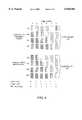
- FIG. 5illustrates the processing in accordance with the above pseudocode in a particular embodiment.
- the vertical columnsrepresent seven consecutive time slots beginning with time slot 1 and ending with time slot 7.
- the upper four rowsrepresent the four ports of controller 300 labeled 328, 330, 332 and 334.
- the four lower rowsrepresent the four input ports of controller 302 labeled 344, 346, 348 and 350.
- Each boxrepresents that state of the A FIFO cell of a port.
- the left half of the boxrepresents the condition of the A cell buffer at the beginning of the time slot and the right half represents the condition of the A cell buffer after a store operation has been performed.
- a shaded halfindicates that a cell is buffered and waiting to be stored and a clear half indicates that the buffer is clear.
- the boxesrepresent the situation where four cells arrive simultaneously at the four input ports of controller 300 in time slot 1 and four cells arrive simultaneously at the four input ports of controller 302 in time slot 3.
- the cell buffered in input port 328 of controller 300is stored and a cell is forwarded.
- the cell buffered in port 330 of controller 300is stored and a cell is forwarded. Operation would continue in this manner until all four cells were stored and four cells were forwarded.
- time slot 3the arrival of four cells in controller 302 in time slot 3 changes matters.
- time slot threethe first of the buffered cells in controller 302 on port 344 is stored and a cell is forwarded.
- the arbitration logicis determining that an input congestion condition is developing as indicated by the assertion of the 2 -- late flag in time slot 3.
- time slot 4the cell buffered in input port 332 of controller 300 is stored and a cell is forwarded, but by now both the 1 -- late and 2 -- late flags have been set.
- the DBL -- RCV flagis set causing the buffered cell on port 334 of controller 300 to be stored and the buffered cell in port 346 to be stored so that no cell is forwarded in this time slot.
- time slots 6 and 7the process reverts back to the normal process and the buffered cells in ports 348 and 350 of controller 302 are stored and two cells are forwarded. From FIG. 5, it can be seen that the buffers of each input port are filled for no longer than five time slots. Since five time slots elapse before a new cell can arrive on an input port, each buffer will be empty to receive a new cell if one should arrive.
- FIG. 6represents that worst case condition in which cells arrive on all four ports of controller 300 and on all four ports of controller 302 at the same time.
- time slot 1the buffered cell on input port 328 is stored and a cell is forwarded.
- a buffered cellis forwarded from port 344 of controller 302 and a cell is forwarded.
- the arbitration circuitryhas recognized an input congestion problem as indicated by the assertion of the 1 -- late and 2 -- late flags.
- the DBL -- RCV flagis asserted causing buffered cells in ports 330 and 346 to be stored and no cell forwarded.
- the DBL -- RCV flagcontinues to be asserted so that cells are stored in ports 332 and 348 in time slot 4 and from ports 334 and 350 in time slot 5.
- each bufferis emptied within five time slots so that a new incoming cell, for example a cell arriving in port 328 in time slot 6 will have a free buffer and will not be lost.
- the memory arbitration processchanges.
- the output process"shares it's bandwidth” with the input process so that the throughput of the switch can be less than the peak possible aggregate input data rate based on the number of input ports while minimizing the possibility of data loss.
- the shared memorycan be used to "smooth out the peaks" and lossless operation at higher utilization is possible. Consequently, lower performance memory subsystems can be used to reduce design cost.
- a very important aspect of this inventionis that, by absorbing the input bursts, it allows flow control protocols the time needed to respond to network traffic conditions and reduce the offered load.
- Flow control protocolsare common and have varying response times.
- Highly effective protocolssuch as FLOW MASTER®, a protocol developed by Digital Equipment Corporation, still require a switch to absorb many cells at the maximum (peak) rate while the protocol reduces the offered load.
- the inventionallows a switch to have reduced throughput without disruption of these protocols.
- the same design, without the inventionwould routinely lose cells when the offered load approached the peak load due to the bursty nature of traffic patterns.
- one of the illustrated embodimentshas input FIFOs with a single B buffer section, it is also possible to use an input FIFO allowing more than one cell to be stored of type B. In this case the inventive bandwidth sharing technique can be invoked only after a set number of cells arrive.
- the above embodimentsrefer to an ATM switch which operates with cells of 53 bytes in length, but the invention is equally applicable to devices having data "packets" of other lengths as well.
Landscapes
- Engineering & Computer Science (AREA)
- Computer Networks & Wireless Communication (AREA)
- Signal Processing (AREA)
- Data Exchanges In Wide-Area Networks (AREA)
Abstract
Description
______________________________________ ARBITRATION PSEUDOCODE ______________________________________ ;Clear flags for beginning of processing 1.sub.-- RCV:=0, 2.sub.-- RCV:=0, DBL.sub.-- RCV:=0, 1.sub.-- late:=0, 2.sub.-- late:=0 loop: Wait: IF (NOT beginning of new slot) then GOTO Wait ELSE ;Begin slot processing ;Determine the arbitration outcome by means of the current cv and late flags 1.sub.-- RCV:=1.sub.-- cv AND NOT (2.sub.-- late AND 2.sub.-- cv) 2.sub.-- RCV:=2.sub.-- cv AND {(NOT 1.sub.-- cv) OR (2.sub.-- late AND 1.sub.-- cv AND NOT 1.sub.-- late)} DBL.sub.-- RCV:=1.sub.-- cv AND 1.sub.-- late AND 2.sub.-- cv AND 2.sub.-- late ;Next determine the late flags for the next slot based on current conditions ;including the result of the arbitration IF (1.sub.-- late =0) then 1.sub.-- late:=(2.sub.-- late AND 1.sub.-- cv AND 2.sub.-- cv) ELSE 1.sub.-- late:=(1.sub.-- cv OR 2.sub.-- cv) ENDIF IF (2.sub.-- late=0)then 2.sub.-- late:=(1.sub.-- cv AND 2.sub.-- cv) ELSE 2.sub.-- late:=(1.sub.-- cv OR 2.sub.-- cv) ENDIF ;Next, do the store and forward operations based on the arbitration outcome IF (1.sub.-- RCV) then forward a cell store a cell from the selected buffer in controller 300 ENDIF IF (2.sub.-- RCV) then forward a cell store a cell from the selected buffer in controller 302 ENDIF IF (DBL.sub.-- RCV) store a cell from the selected buffer in controller 300 store a cell from the selected buffer in controller 302 ENDIF ;clear the arbitration fJags for the next time slot 1.sub.-- RCV:=0 2.sub.-- RCV:=0 DBL.sub.-- RCV:=0 ;repeat processing for next time slot ENDIF GOTO loop ______________________________________Claims (29)
Priority Applications (1)
| Application Number | Priority Date | Filing Date | Title |
|---|---|---|---|
| US08/819,273US6046982A (en) | 1997-03-18 | 1997-03-18 | Method and apparatus for reducing data loss in data transfer devices |
Applications Claiming Priority (1)
| Application Number | Priority Date | Filing Date | Title |
|---|---|---|---|
| US08/819,273US6046982A (en) | 1997-03-18 | 1997-03-18 | Method and apparatus for reducing data loss in data transfer devices |
Publications (1)
| Publication Number | Publication Date |
|---|---|
| US6046982Atrue US6046982A (en) | 2000-04-04 |
Family
ID=25227673
Family Applications (1)
| Application Number | Title | Priority Date | Filing Date |
|---|---|---|---|
| US08/819,273Expired - LifetimeUS6046982A (en) | 1997-03-18 | 1997-03-18 | Method and apparatus for reducing data loss in data transfer devices |
Country Status (1)
| Country | Link |
|---|---|
| US (1) | US6046982A (en) |
Cited By (16)
| Publication number | Priority date | Publication date | Assignee | Title |
|---|---|---|---|---|
| US20010022786A1 (en)* | 1998-04-20 | 2001-09-20 | Wai King | Receive processing for dedicated bandwidth data communication switch backplane |
| US6314487B1 (en)* | 1997-12-26 | 2001-11-06 | Electronics And Telecommunications Research Institute | Adaptive routing controller of a crossbar core module used in a crossbar routing switch |
| US20020006112A1 (en)* | 2000-05-05 | 2002-01-17 | Jaber Abed Mohd | Method and system for modeling and advertising asymmetric topology of a node in a transport network |
| US6457106B1 (en)* | 1997-07-22 | 2002-09-24 | Nec Corporation | Shared memory control system and shared memory control method |
| US20040081169A1 (en)* | 2002-10-29 | 2004-04-29 | Kloth Axel K. | Pseudo synchronous machine |
| US20040139259A1 (en)* | 2003-01-15 | 2004-07-15 | Mantey Paul J. | Systems and methods for accessing bus-mastered system resources |
| US20040220863A1 (en)* | 2003-04-29 | 2004-11-04 | International Business Machines Corporation | Saved subset of configurable offering as a basis for future orders |
| US6829647B1 (en)* | 2000-06-09 | 2004-12-07 | International Business Machines Corporation | Scaleable hardware arbiter |
| US6831922B1 (en)* | 1999-05-12 | 2004-12-14 | Nec Corporation | Contention priority control circuit |
| US20070140232A1 (en)* | 2005-12-16 | 2007-06-21 | Carson Mark B | Self-steering Clos switch |
| US20080027738A1 (en)* | 2006-07-31 | 2008-01-31 | Microsoft Corporation | Increasing business value through increased usage and adoption |
| US20080028157A1 (en)* | 2003-01-13 | 2008-01-31 | Steinmetz Joseph H | Global shared memory switch |
| US20080250116A1 (en)* | 2000-07-24 | 2008-10-09 | Mosaid Technologies Incorporated | Method and apparatus for reducing pool starvation in a shared memory switch |
| US20110019548A1 (en)* | 2000-09-13 | 2011-01-27 | Juniper Networks, Inc. | Traffic arbitration |
| US7881194B1 (en)* | 2005-08-10 | 2011-02-01 | Sawyer Law Group, P.C. | Method for pacing multi-rate time sensitive traffic on ethernet and bridge connected networks |
| CN102684959A (en)* | 2011-03-18 | 2012-09-19 | 联发科技股份有限公司 | Method for sharing Ethernet circuit by electronic device and multiple ports |
Citations (18)
| Publication number | Priority date | Publication date | Assignee | Title |
|---|---|---|---|---|
| US5072363A (en)* | 1989-12-22 | 1991-12-10 | Harris Corporation | Multimode resource arbiter providing round robin arbitration or a modified priority arbitration |
| US5157654A (en)* | 1990-12-18 | 1992-10-20 | Bell Communications Research, Inc. | Technique for resolving output port contention in a high speed packet switch |
| US5276842A (en)* | 1990-04-10 | 1994-01-04 | Mitsubishi Denki Kabushiki Kaisha | Dual port memory |
| US5276887A (en)* | 1991-06-06 | 1994-01-04 | Commodore Electronics Limited | Bus arbitration system for granting bus access to devices following two-wire bus arbitration protocol and devices following three-wire bus arbitration protocol |
| US5301333A (en)* | 1990-06-14 | 1994-04-05 | Bell Communications Research, Inc. | Tree structured variable priority arbitration implementing a round-robin scheduling policy |
| US5394397A (en)* | 1992-03-27 | 1995-02-28 | Hitachi, Ltd. | Shared buffer memory type ATM communication system and method with a broadcast facility |
| US5436886A (en)* | 1994-07-14 | 1995-07-25 | Northern Telecom Limited | ATM switch in dual switch plane operation |
| US5438666A (en)* | 1988-08-11 | 1995-08-01 | Ast Research, Inc. | Shared memory bus system for arbitrating access control among contending memory refresh circuits, peripheral controllers, and bus masters |
| US5440698A (en)* | 1990-11-30 | 1995-08-08 | Xerox Corporation | Arbitration of packet switched busses, including busses for shared memory multiprocessors |
| US5517495A (en)* | 1994-12-06 | 1996-05-14 | At&T Corp. | Fair prioritized scheduling in an input-buffered switch |
| US5553061A (en)* | 1994-06-27 | 1996-09-03 | Loral Fairchild Corporation | Packet processor having service priority and loss priority features |
| US5577035A (en)* | 1994-03-23 | 1996-11-19 | Roke Manor Research Limited | Apparatus and method of processing bandwidth requirements in an ATM switch |
| US5619495A (en)* | 1994-09-02 | 1997-04-08 | Mitsubishi Denki Kabushiki Kaisha | Cell switching apparatus and a cell switching system |
| US5696764A (en)* | 1993-07-21 | 1997-12-09 | Fujitsu Limited | ATM exchange for monitoring congestion and allocating and transmitting bandwidth-guaranteed and non-bandwidth-guaranteed connection calls |
| US5748629A (en)* | 1995-07-19 | 1998-05-05 | Fujitsu Networks Communications, Inc. | Allocated and dynamic bandwidth management |
| US5805577A (en)* | 1995-07-20 | 1998-09-08 | Jain; Raj | Erica: explicit rate indication for congestion avoidance in ATM networks |
| US5818818A (en)* | 1995-09-26 | 1998-10-06 | Fujitsu Limited | Communication service quality control system |
| US5838677A (en)* | 1995-04-18 | 1998-11-17 | Hitachi, Ltd. | Switching system having means for congestion control by monitoring packets in a shared buffer and by suppressing the reading of packets from input buffers |
- 1997
- 1997-03-18USUS08/819,273patent/US6046982A/ennot_activeExpired - Lifetime
Patent Citations (19)
| Publication number | Priority date | Publication date | Assignee | Title |
|---|---|---|---|---|
| US5438666A (en)* | 1988-08-11 | 1995-08-01 | Ast Research, Inc. | Shared memory bus system for arbitrating access control among contending memory refresh circuits, peripheral controllers, and bus masters |
| US5072363A (en)* | 1989-12-22 | 1991-12-10 | Harris Corporation | Multimode resource arbiter providing round robin arbitration or a modified priority arbitration |
| US5276842A (en)* | 1990-04-10 | 1994-01-04 | Mitsubishi Denki Kabushiki Kaisha | Dual port memory |
| US5301333A (en)* | 1990-06-14 | 1994-04-05 | Bell Communications Research, Inc. | Tree structured variable priority arbitration implementing a round-robin scheduling policy |
| US5440698A (en)* | 1990-11-30 | 1995-08-08 | Xerox Corporation | Arbitration of packet switched busses, including busses for shared memory multiprocessors |
| US5157654A (en)* | 1990-12-18 | 1992-10-20 | Bell Communications Research, Inc. | Technique for resolving output port contention in a high speed packet switch |
| US5276887A (en)* | 1991-06-06 | 1994-01-04 | Commodore Electronics Limited | Bus arbitration system for granting bus access to devices following two-wire bus arbitration protocol and devices following three-wire bus arbitration protocol |
| US5394397A (en)* | 1992-03-27 | 1995-02-28 | Hitachi, Ltd. | Shared buffer memory type ATM communication system and method with a broadcast facility |
| US5696764A (en)* | 1993-07-21 | 1997-12-09 | Fujitsu Limited | ATM exchange for monitoring congestion and allocating and transmitting bandwidth-guaranteed and non-bandwidth-guaranteed connection calls |
| US5577035A (en)* | 1994-03-23 | 1996-11-19 | Roke Manor Research Limited | Apparatus and method of processing bandwidth requirements in an ATM switch |
| US5553061A (en)* | 1994-06-27 | 1996-09-03 | Loral Fairchild Corporation | Packet processor having service priority and loss priority features |
| US5436886A (en)* | 1994-07-14 | 1995-07-25 | Northern Telecom Limited | ATM switch in dual switch plane operation |
| US5619495A (en)* | 1994-09-02 | 1997-04-08 | Mitsubishi Denki Kabushiki Kaisha | Cell switching apparatus and a cell switching system |
| US5517495A (en)* | 1994-12-06 | 1996-05-14 | At&T Corp. | Fair prioritized scheduling in an input-buffered switch |
| US5838677A (en)* | 1995-04-18 | 1998-11-17 | Hitachi, Ltd. | Switching system having means for congestion control by monitoring packets in a shared buffer and by suppressing the reading of packets from input buffers |
| US5748629A (en)* | 1995-07-19 | 1998-05-05 | Fujitsu Networks Communications, Inc. | Allocated and dynamic bandwidth management |
| US5787086A (en)* | 1995-07-19 | 1998-07-28 | Fujitsu Network Communications, Inc. | Method and apparatus for emulating a circuit connection in a cell based communications network |
| US5805577A (en)* | 1995-07-20 | 1998-09-08 | Jain; Raj | Erica: explicit rate indication for congestion avoidance in ATM networks |
| US5818818A (en)* | 1995-09-26 | 1998-10-06 | Fujitsu Limited | Communication service quality control system |
Cited By (33)
| Publication number | Priority date | Publication date | Assignee | Title |
|---|---|---|---|---|
| US6457106B1 (en)* | 1997-07-22 | 2002-09-24 | Nec Corporation | Shared memory control system and shared memory control method |
| US6314487B1 (en)* | 1997-12-26 | 2001-11-06 | Electronics And Telecommunications Research Institute | Adaptive routing controller of a crossbar core module used in a crossbar routing switch |
| US20010022786A1 (en)* | 1998-04-20 | 2001-09-20 | Wai King | Receive processing for dedicated bandwidth data communication switch backplane |
| US6931019B2 (en)* | 1998-04-20 | 2005-08-16 | Alcatel | Receive processing for dedicated bandwidth data communication switch backplane |
| US6831922B1 (en)* | 1999-05-12 | 2004-12-14 | Nec Corporation | Contention priority control circuit |
| US20020006112A1 (en)* | 2000-05-05 | 2002-01-17 | Jaber Abed Mohd | Method and system for modeling and advertising asymmetric topology of a node in a transport network |
| US7173912B2 (en)* | 2000-05-05 | 2007-02-06 | Fujitsu Limited | Method and system for modeling and advertising asymmetric topology of a node in a transport network |
| US6829647B1 (en)* | 2000-06-09 | 2004-12-07 | International Business Machines Corporation | Scaleable hardware arbiter |
| US20080250116A1 (en)* | 2000-07-24 | 2008-10-09 | Mosaid Technologies Incorporated | Method and apparatus for reducing pool starvation in a shared memory switch |
| US20100250699A1 (en)* | 2000-07-24 | 2010-09-30 | Mosaid Technologies Incorporated | Method and apparatus for reducing pool starvation in a shared memory switch |
| US9083659B2 (en) | 2000-07-24 | 2015-07-14 | Conversant Intellectual Property Management Inc. | Method and apparatus for reducing pool starvation in a shared memory switch |
| US8630304B2 (en) | 2000-07-24 | 2014-01-14 | Mosaid Technologies Incorporated | Method and apparatus for reducing pool starvation in a shared memory switch |
| US7996485B2 (en) | 2000-07-24 | 2011-08-09 | Mosaid Technologies Incorporated | Method and apparatus for reducing pool starvation in a shared memory switch |
| US7743108B2 (en)* | 2000-07-24 | 2010-06-22 | Mosaid Technologies Incorporated | Method and apparatus for reducing pool starvation in a shared memory switch |
| US8705358B2 (en)* | 2000-09-13 | 2014-04-22 | Juniper Networks, Inc. | Traffic arbitration |
| US20110019548A1 (en)* | 2000-09-13 | 2011-01-27 | Juniper Networks, Inc. | Traffic arbitration |
| US7324524B2 (en)* | 2002-10-29 | 2008-01-29 | Mindspeed Technologies, Inc. | Pseudo synchronous machine |
| US20040081169A1 (en)* | 2002-10-29 | 2004-04-29 | Kloth Axel K. | Pseudo synchronous machine |
| US20080028157A1 (en)* | 2003-01-13 | 2008-01-31 | Steinmetz Joseph H | Global shared memory switch |
| US20160021031A1 (en)* | 2003-01-13 | 2016-01-21 | Avago Technologies General Ip (Singapore) Pte. Ltd. | Global shared memory switch |
| US20040139259A1 (en)* | 2003-01-15 | 2004-07-15 | Mantey Paul J. | Systems and methods for accessing bus-mastered system resources |
| US7039736B2 (en)* | 2003-01-15 | 2006-05-02 | Hewlett-Packard Development Company, L.P. | Systems and methods for accessing bus-mastered system resources |
| US20040220863A1 (en)* | 2003-04-29 | 2004-11-04 | International Business Machines Corporation | Saved subset of configurable offering as a basis for future orders |
| US7881194B1 (en)* | 2005-08-10 | 2011-02-01 | Sawyer Law Group, P.C. | Method for pacing multi-rate time sensitive traffic on ethernet and bridge connected networks |
| US20110116371A1 (en)* | 2005-08-10 | 2011-05-19 | Sawyer Law Group, P.C. | Method for pacing multi-rate time sensitive traffic on ethernet and bridge connected networks |
| US8619567B2 (en) | 2005-08-10 | 2013-12-31 | Sawyer Law Group, P.C. | Method for pacing multi-rate time sensitive traffic on Ethernet and bridge connected networks |
| US20070140232A1 (en)* | 2005-12-16 | 2007-06-21 | Carson Mark B | Self-steering Clos switch |
| US20080027738A1 (en)* | 2006-07-31 | 2008-01-31 | Microsoft Corporation | Increasing business value through increased usage and adoption |
| US8724621B2 (en)* | 2011-03-18 | 2014-05-13 | Mediatek Inc. | Electronic apparatus and method for sharing ethernet circuit between plurality of ports |
| CN102684959B (en)* | 2011-03-18 | 2014-12-17 | 联发科技股份有限公司 | Electronic device and method for sharing Ethernet circuit with multiple ports |
| TWI467970B (en)* | 2011-03-18 | 2015-01-01 | Mediatek Inc | Electronic apparatus and method for sharing ethernet circuit between plurality of ports |
| US20120236852A1 (en)* | 2011-03-18 | 2012-09-20 | Mediatek Inc. | Electronic apparatus and method for sharing ethernet circuit between plurality of ports |
| CN102684959A (en)* | 2011-03-18 | 2012-09-19 | 联发科技股份有限公司 | Method for sharing Ethernet circuit by electronic device and multiple ports |
Similar Documents
| Publication | Publication Date | Title |
|---|---|---|
| JP4006205B2 (en) | Switching arrangement and method with separate output buffers | |
| CA2329542C (en) | System and method for scheduling message transmission and processing in a digital data network | |
| US5457687A (en) | Method and apparatus for backward explicit congestion notification (BECN) in an ATM network | |
| JP4080888B2 (en) | Switching mechanism and method having separate outputs | |
| US6999415B2 (en) | Switching device and method for controlling the routing of data packets | |
| EP0687091B1 (en) | Method of regulating backpressure traffic in a packet switched network | |
| US6907041B1 (en) | Communications interconnection network with distributed resequencing | |
| US7283471B2 (en) | System and method for regulating message flow in a digital data network | |
| US5379297A (en) | Concurrent multi-channel segmentation and reassembly processors for asynchronous transfer mode | |
| EP0858717B1 (en) | Improvements in or relating to an atm switch | |
| US6046982A (en) | Method and apparatus for reducing data loss in data transfer devices | |
| JP2000261506A (en) | Rate controlled multi-class large capacity packet switch | |
| JPH10512422A (en) | Large capacity ATM switch | |
| EP1016246A1 (en) | Networking systems | |
| JPH08265331A (en) | Flow control device and flow control method | |
| GB2365665A (en) | Switching arrangement for data packets | |
| US6574232B1 (en) | Crossbar switch utilizing broadcast buffer and associated broadcast buffer management unit | |
| US8706896B2 (en) | Guaranteed bandwidth memory apparatus and method | |
| US7130301B2 (en) | Self-route expandable multi-memory packet switch with distributed scheduling means | |
| EP1133110B1 (en) | Switching device and method | |
| US6553035B1 (en) | Apparatus and method for queuing data | |
| EP0604538B1 (en) | Method and apparatus for asynchronous transfer mode (atm) network | |
| Obara et al. | High speed transport processor for broad-band burst transport system | |
| EP1198098B1 (en) | Switching arrangement and method with separated output buffers | |
| JP4504606B2 (en) | Apparatus and method for shaping traffic in a network switch |
Legal Events
| Date | Code | Title | Description |
|---|---|---|---|
| AS | Assignment | Owner name:DIGITAL EQUIPMENT CORP., MASSACHUSETTS Free format text:ASSIGNMENT OF ASSIGNORS INTEREST;ASSIGNORS:GRELLA, ERNEST;COOPER, JEFFREY L.;REEL/FRAME:008793/0486 Effective date:19970318 | |
| AS | Assignment | Owner name:DIGITAL EQUIPMENT CORPORATION, MASSACHUSETTS Free format text:ASSIGNMENT OF ASSIGNORS INTEREST;ASSIGNOR:OZVEREN, CUNEYT M.;REEL/FRAME:008622/0647 Effective date:19970708 | |
| AS | Assignment | Owner name:CABLETRON SYSTEMS, INC., NEW HAMPSHIRE Free format text:ASSIGNMENT OF ASSIGNORS INTEREST;ASSIGNOR:DIGITAL EQUIPMENT CORPORATION;REEL/FRAME:009050/0477 Effective date:19980206 | |
| AS | Assignment | Owner name:DIGITAL EQUIPMENT CORPORATION, MASSACHUSETTS Free format text:CORRECTED ASSIGNMENT TO ADD CONVEYING PARTIES NAMES. AN ASSIGNMENT WAS PREVIOUSLY RECORDED AT REEL 8793 FRAME 0486.;ASSIGNORS:GRELLA, ERNEST;COOPER, JEFFREY L.;HUTCHINSON, JERRY D.;REEL/FRAME:009432/0582 Effective date:19970318 | |
| FEPP | Fee payment procedure | Free format text:PAYOR NUMBER ASSIGNED (ORIGINAL EVENT CODE: ASPN); ENTITY STATUS OF PATENT OWNER: LARGE ENTITY | |
| STCF | Information on status: patent grant | Free format text:PATENTED CASE | |
| AS | Assignment | Owner name:ENTERASYS NETWORKS, INC., NEW HAMPSHIRE Free format text:ASSIGNMENT OF ASSIGNORS INTEREST;ASSIGNOR:CABLETRON SYSTEMS, INC.;REEL/FRAME:011219/0376 Effective date:20000929 | |
| FPAY | Fee payment | Year of fee payment:4 | |
| REMI | Maintenance fee reminder mailed | ||
| AS | Assignment | Owner name:OBSIDIAN, LLC, CALIFORNIA Free format text:SECURITY AGREEMENT;ASSIGNOR:ENTERASYS NETWORKS, INC.;REEL/FRAME:017656/0552 Effective date:20060516 Owner name:WELLS FARGO FOOTHILL, INC., CALIFORNIA Free format text:SECURITY AGREEMENT;ASSIGNOR:ENTERASYS NETWORKS, INC.;REEL/FRAME:017656/0552 Effective date:20060516 | |
| FPAY | Fee payment | Year of fee payment:8 | |
| AS | Assignment | Owner name:WELLS FARGO TRUST CORPORATION LIMITED, AS SECURITY Free format text:GRANT OF SECURITY INTEREST IN U.S. PATENTS;ASSIGNOR:ENTERASYS NETWORKS INC.;REEL/FRAME:025339/0875 Effective date:20101109 | |
| AS | Assignment | Owner name:ENTERASYS NETWORKS, INC., MASSACHUSETTS Free format text:RELEASE AND REASSIGNMENT OF PATENTS AND PATENT APPLICATIONS AT REEL/FRAME NO. 17656/0552;ASSIGNORS:WELLS FARGO CAPITAL FINANCE, INC. (FORMERLY KNOWN AS WELLS FARGO FOOTHILL, INC.);ENTERPRISE COMMUNICATIONS FUNDING GMBH, AS SUCCESSOR IN INTEREST TO OBSIDIAN, LLC;REEL/FRAME:025406/0769 Effective date:20101110 | |
| FPAY | Fee payment | Year of fee payment:12 | |
| AS | Assignment | Owner name:ENTERASYS NETWORKS INC., MASSACHUSETTS Free format text:TERMINATION AND RELEASE OF SECURITY INTEREST IN PATENTS AT REEL/FRAME NO. 25339/0875;ASSIGNOR:WELLS FARGO TRUST CORPORATION LIMITED;REEL/FRAME:031558/0677 Effective date:20131031 | |
| AS | Assignment | Owner name:SILICON VALLEY BANK, CALIFORNIA Free format text:SECURITY AGREEMENT;ASSIGNOR:ENTERASYS NETWORKS, INC.;REEL/FRAME:036189/0509 Effective date:20150724 | |
| AS | Assignment | Owner name:EXTREME NETWORKS, INC., NEW HAMPSHIRE Free format text:ASSIGNMENT OF ASSIGNORS INTEREST;ASSIGNOR:ENTERASYS NETWORKS, INC.;REEL/FRAME:036467/0566 Effective date:20150820 | |
| AS | Assignment | Owner name:EXTREME NETWORKS, INC., CALIFORNIA Free format text:ASSIGNMENT OF ASSIGNORS INTEREST;ASSIGNOR:ENTERASYS NETWORKS, INC.;REEL/FRAME:036538/0011 Effective date:20150820 | |
| AS | Assignment | Owner name:SILICON VALLEY BANK, CALIFORNIA Free format text:AMENDED AND RESTATED PATENT AND TRADEMARK SECURITY AGREEMENT;ASSIGNOR:EXTREME NETWORKS, INC.;REEL/FRAME:040521/0762 Effective date:20161028 | |
| AS | Assignment | Owner name:SILICON VALLEY BANK, CALIFORNIA Free format text:SECOND AMENDED AND RESTATED PATENT AND TRADEMARK SECURITY AGREEMENT;ASSIGNOR:EXTREME NETWORKS, INC.;REEL/FRAME:043200/0614 Effective date:20170714 | |
| AS | Assignment | Owner name:ENTERASYS NETWORKS, INC., CALIFORNIA Free format text:RELEASE BY SECURED PARTY;ASSIGNOR:SILICON VALLEY BANK;REEL/FRAME:046047/0223 Effective date:20180501 Owner name:BANK OF MONTREAL, NEW YORK Free format text:SECURITY INTEREST;ASSIGNOR:EXTREME NETWORKS, INC.;REEL/FRAME:046050/0546 Effective date:20180501 Owner name:EXTREME NETWORKS, INC., CALIFORNIA Free format text:RELEASE BY SECURED PARTY;ASSIGNOR:SILICON VALLEY BANK;REEL/FRAME:046051/0775 Effective date:20180501 |