US6046111A - Method and apparatus for endpointing mechanical and chemical-mechanical planarization of microelectronic substrates - Google Patents
Method and apparatus for endpointing mechanical and chemical-mechanical planarization of microelectronic substratesDownload PDFInfo
- Publication number
- US6046111A US6046111AUS09/146,330US14633098AUS6046111AUS 6046111 AUS6046111 AUS 6046111AUS 14633098 AUS14633098 AUS 14633098AUS 6046111 AUS6046111 AUS 6046111A
- Authority
- US
- United States
- Prior art keywords
- substrate
- planarizing
- fluid
- polishing pad
- viscosity
- Prior art date
- Legal status (The legal status is an assumption and is not a legal conclusion. Google has not performed a legal analysis and makes no representation as to the accuracy of the status listed.)
- Expired - Lifetime
Links
- 239000000758substrateSubstances0.000titleclaimsabstractdescription285
- 238000000034methodMethods0.000titleclaimsabstractdescription87
- 238000004377microelectronicMethods0.000titleclaimsabstractdescription23
- 239000012530fluidSubstances0.000claimsabstractdescription154
- 239000002245particleSubstances0.000claimsabstractdescription103
- 238000005498polishingMethods0.000claimsabstractdescription100
- 239000000463materialSubstances0.000claimsabstractdescription48
- 239000006193liquid solutionSubstances0.000claimsdescription31
- 239000004816latexSubstances0.000claimsdescription21
- 229920000126latexPolymers0.000claimsdescription21
- VYPSYNLAJGMNEJ-UHFFFAOYSA-NSilicium dioxideChemical compoundO=[Si]=OVYPSYNLAJGMNEJ-UHFFFAOYSA-N0.000claimsdescription18
- QGZKDVFQNNGYKY-UHFFFAOYSA-NAmmoniaChemical compoundNQGZKDVFQNNGYKY-UHFFFAOYSA-N0.000claimsdescription10
- 229910000420cerium oxideInorganic materials0.000claimsdescription9
- TWNQGVIAIRXVLR-UHFFFAOYSA-Noxo(oxoalumanyloxy)alumaneChemical compoundO=[Al]O[Al]=OTWNQGVIAIRXVLR-UHFFFAOYSA-N0.000claimsdescription8
- BMMGVYCKOGBVEV-UHFFFAOYSA-Noxo(oxoceriooxy)ceriumChemical compound[Ce]=O.O=[Ce]=OBMMGVYCKOGBVEV-UHFFFAOYSA-N0.000claimsdescription8
- BPUBBGLMJRNUCC-UHFFFAOYSA-Noxygen(2-);tantalum(5+)Chemical compound[O-2].[O-2].[O-2].[O-2].[O-2].[Ta+5].[Ta+5]BPUBBGLMJRNUCC-UHFFFAOYSA-N0.000claimsdescription8
- 229910001936tantalum oxideInorganic materials0.000claimsdescription8
- 230000007423decreaseEffects0.000claimsdescription6
- 239000000523sampleSubstances0.000claimsdescription6
- 229910021529ammoniaInorganic materials0.000claimsdescription5
- 229910052814silicon oxideInorganic materials0.000claimsdescription4
- ZLMJMSJWJFRBEC-UHFFFAOYSA-NPotassiumChemical compound[K]ZLMJMSJWJFRBEC-UHFFFAOYSA-N0.000claimsdescription3
- 229910052700potassiumInorganic materials0.000claimsdescription3
- 239000011591potassiumSubstances0.000claimsdescription3
- 229920000642polymerPolymers0.000claimsdescription2
- GWEVSGVZZGPLCZ-UHFFFAOYSA-NTitan oxideChemical compoundO=[Ti]=OGWEVSGVZZGPLCZ-UHFFFAOYSA-N0.000claims7
- OGIDPMRJRNCKJF-UHFFFAOYSA-Ntitanium oxideInorganic materials[Ti]=OOGIDPMRJRNCKJF-UHFFFAOYSA-N0.000claims7
- 238000000151depositionMethods0.000claims6
- 235000012239silicon dioxideNutrition0.000claims5
- 239000000377silicon dioxideSubstances0.000claims5
- 238000003825pressingMethods0.000claims3
- 230000003247decreasing effectEffects0.000claims1
- 235000012431wafersNutrition0.000abstractdescription8
- 239000004065semiconductorSubstances0.000abstractdescription4
- 238000012545processingMethods0.000description17
- 239000002002slurrySubstances0.000description6
- 238000002955isolationMethods0.000description4
- 238000004519manufacturing processMethods0.000description3
- 239000000126substanceSubstances0.000description3
- 239000008119colloidal silicaSubstances0.000description2
- 229910021485fumed silicaInorganic materials0.000description2
- PNEYBMLMFCGWSK-UHFFFAOYSA-NAluminaChemical class[O-2].[O-2].[O-2].[Al+3].[Al+3]PNEYBMLMFCGWSK-UHFFFAOYSA-N0.000description1
- 239000004372Polyvinyl alcoholSubstances0.000description1
- 239000011324beadSubstances0.000description1
- DRVWBEJJZZTIGJ-UHFFFAOYSA-Ncerium(3+);oxygen(2-)Chemical class[O-2].[O-2].[O-2].[Ce+3].[Ce+3]DRVWBEJJZZTIGJ-UHFFFAOYSA-N0.000description1
- 230000002860competitive effectEffects0.000description1
- 238000007796conventional methodMethods0.000description1
- 238000001514detection methodMethods0.000description1
- 238000010586diagramMethods0.000description1
- 239000007788liquidSubstances0.000description1
- AMWRITDGCCNYAT-UHFFFAOYSA-Lmanganese oxideInorganic materials[Mn].O[Mn]=O.O[Mn]=OAMWRITDGCCNYAT-UHFFFAOYSA-L0.000description1
- PPNAOCWZXJOHFK-UHFFFAOYSA-Nmanganese(2+);oxygen(2-)Chemical class[O-2].[Mn+2]PPNAOCWZXJOHFK-UHFFFAOYSA-N0.000description1
- 238000005259measurementMethods0.000description1
- 238000012986modificationMethods0.000description1
- 230000004048modificationEffects0.000description1
- 150000004767nitridesChemical class0.000description1
- 229920002635polyurethanePolymers0.000description1
- 239000004814polyurethaneSubstances0.000description1
- 229920002451polyvinyl alcoholPolymers0.000description1
- LIVNPJMFVYWSIS-UHFFFAOYSA-Nsilicon monoxideChemical class[Si-]#[O+]LIVNPJMFVYWSIS-UHFFFAOYSA-N0.000description1
- 239000000725suspensionSubstances0.000description1
Images


Classifications
- B—PERFORMING OPERATIONS; TRANSPORTING
- B24—GRINDING; POLISHING
- B24B—MACHINES, DEVICES, OR PROCESSES FOR GRINDING OR POLISHING; DRESSING OR CONDITIONING OF ABRADING SURFACES; FEEDING OF GRINDING, POLISHING, OR LAPPING AGENTS
- B24B37/00—Lapping machines or devices; Accessories
- B24B37/005—Control means for lapping machines or devices
- B24B37/013—Devices or means for detecting lapping completion
- B—PERFORMING OPERATIONS; TRANSPORTING
- B24—GRINDING; POLISHING
- B24B—MACHINES, DEVICES, OR PROCESSES FOR GRINDING OR POLISHING; DRESSING OR CONDITIONING OF ABRADING SURFACES; FEEDING OF GRINDING, POLISHING, OR LAPPING AGENTS
- B24B37/00—Lapping machines or devices; Accessories
- B24B37/005—Control means for lapping machines or devices
- B24B37/015—Temperature control
- B—PERFORMING OPERATIONS; TRANSPORTING
- B24—GRINDING; POLISHING
- B24B—MACHINES, DEVICES, OR PROCESSES FOR GRINDING OR POLISHING; DRESSING OR CONDITIONING OF ABRADING SURFACES; FEEDING OF GRINDING, POLISHING, OR LAPPING AGENTS
- B24B37/00—Lapping machines or devices; Accessories
- B24B37/04—Lapping machines or devices; Accessories designed for working plane surfaces
- B24B37/042—Lapping machines or devices; Accessories designed for working plane surfaces operating processes therefor
- B24B37/044—Lapping machines or devices; Accessories designed for working plane surfaces operating processes therefor characterised by the composition of the lapping agent
- B—PERFORMING OPERATIONS; TRANSPORTING
- B24—GRINDING; POLISHING
- B24B—MACHINES, DEVICES, OR PROCESSES FOR GRINDING OR POLISHING; DRESSING OR CONDITIONING OF ABRADING SURFACES; FEEDING OF GRINDING, POLISHING, OR LAPPING AGENTS
- B24B37/00—Lapping machines or devices; Accessories
- B24B37/04—Lapping machines or devices; Accessories designed for working plane surfaces
- B24B37/07—Lapping machines or devices; Accessories designed for working plane surfaces characterised by the movement of the work or lapping tool
- B24B37/10—Lapping machines or devices; Accessories designed for working plane surfaces characterised by the movement of the work or lapping tool for single side lapping
- B24B37/105—Lapping machines or devices; Accessories designed for working plane surfaces characterised by the movement of the work or lapping tool for single side lapping the workpieces or work carriers being actively moved by a drive, e.g. in a combined rotary and translatory movement
- B—PERFORMING OPERATIONS; TRANSPORTING
- B24—GRINDING; POLISHING
- B24B—MACHINES, DEVICES, OR PROCESSES FOR GRINDING OR POLISHING; DRESSING OR CONDITIONING OF ABRADING SURFACES; FEEDING OF GRINDING, POLISHING, OR LAPPING AGENTS
- B24B49/00—Measuring or gauging equipment for controlling the feed movement of the grinding tool or work; Arrangements of indicating or measuring equipment, e.g. for indicating the start of the grinding operation
- B24B49/10—Measuring or gauging equipment for controlling the feed movement of the grinding tool or work; Arrangements of indicating or measuring equipment, e.g. for indicating the start of the grinding operation involving electrical means
- B—PERFORMING OPERATIONS; TRANSPORTING
- B24—GRINDING; POLISHING
- B24B—MACHINES, DEVICES, OR PROCESSES FOR GRINDING OR POLISHING; DRESSING OR CONDITIONING OF ABRADING SURFACES; FEEDING OF GRINDING, POLISHING, OR LAPPING AGENTS
- B24B49/00—Measuring or gauging equipment for controlling the feed movement of the grinding tool or work; Arrangements of indicating or measuring equipment, e.g. for indicating the start of the grinding operation
- B24B49/12—Measuring or gauging equipment for controlling the feed movement of the grinding tool or work; Arrangements of indicating or measuring equipment, e.g. for indicating the start of the grinding operation involving optical means
- B—PERFORMING OPERATIONS; TRANSPORTING
- B24—GRINDING; POLISHING
- B24B—MACHINES, DEVICES, OR PROCESSES FOR GRINDING OR POLISHING; DRESSING OR CONDITIONING OF ABRADING SURFACES; FEEDING OF GRINDING, POLISHING, OR LAPPING AGENTS
- B24B49/00—Measuring or gauging equipment for controlling the feed movement of the grinding tool or work; Arrangements of indicating or measuring equipment, e.g. for indicating the start of the grinding operation
- B24B49/14—Measuring or gauging equipment for controlling the feed movement of the grinding tool or work; Arrangements of indicating or measuring equipment, e.g. for indicating the start of the grinding operation taking regard of the temperature during grinding
- B—PERFORMING OPERATIONS; TRANSPORTING
- B24—GRINDING; POLISHING
- B24B—MACHINES, DEVICES, OR PROCESSES FOR GRINDING OR POLISHING; DRESSING OR CONDITIONING OF ABRADING SURFACES; FEEDING OF GRINDING, POLISHING, OR LAPPING AGENTS
- B24B49/00—Measuring or gauging equipment for controlling the feed movement of the grinding tool or work; Arrangements of indicating or measuring equipment, e.g. for indicating the start of the grinding operation
- B24B49/16—Measuring or gauging equipment for controlling the feed movement of the grinding tool or work; Arrangements of indicating or measuring equipment, e.g. for indicating the start of the grinding operation taking regard of the load
Definitions
- the present inventionrelates to devices and methods for measuring the endpoint of a microelectronic substrate in mechanical and chemical-mechanical planarizing processes.
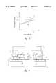
- FIG. 1schematically illustrates a planarizing machine 10 with a platen or table 20, a carrier assembly 30, a polishing pad 40, and a planarizing fluid 44 on the polishing pad 40.
- the planarizing machine 10may also have an under-pad 25 attached to an upper surface 22 of the platen 20 for supporting the polishing pad 40.
- a drive assembly 26rotates (arrow A) and/or reciprocates (arrow B) the platen 20 to move the polishing pad 40 during planarization.
- the carrier assembly 30controls and protects a substrate 12 during planarization.
- the carrier assembly 30typically has a substrate holder 32 with a pad 34 that holds the substrate 12 via suction.
- a drive assembly 36 of the carrier assembly 30typically rotates and/or translates the substrate holder 32 (arrows C and D, respectively).
- the substrate holder 32may be a weighted, free-floating disk (not shown) that slides over the polishing pad 40.
- the combination of the polishing pad 40 and the planarizing fluid 44generally define a planarizing medium that mechanically and/or chemically-mechanically removes material from the surface of the substrate 12.
- the polishing pad 40may be a conventional polishing pad composed of a polymeric material (e.g., polyurethane) without abrasive particles, or it may be an abrasive polishing pad with abrasive particles fixedly bonded to a suspension material.
- the planarizing fluid 44may be a CMP slurry with abrasive particles and chemicals for use with a conventional nonabrasive polishing pad.
- the planarizing fluid 44may be a chemical solution without abrasive particles for use with an abrasive polishing pad.
- the carrier assembly 30presses the substrate 12 against a planarizing surface 42 of the polishing pad 40 in the presence of the planarizing fluid 44.
- the platen 20 and/or the substrate holder 32then move relative to one another to translate the substrate 12 across the planarizing surface 42.
- the abrasive particles and/or the chemicals in the planarizing mediumremove material from the surface of the substrate 12.
- CMP processesmust consistently and accurately produce a uniformly planar surface on the substrate to enable precise fabrication of circuits and photo-patterns.
- substratesPrior to being planarized, many substrates have large "step heights" that create a highly topographic surface across the substrate. Yet, as the density of integrated circuits increases, it is necessary to have a planar substrate surface at several stages of processing the substrate because non-uniform substrate surfaces significantly increase the difficulty of forming sub-micron features or photo-patterns to within a tolerance of approximately 0.1 ⁇ m.
- CMP processesmust typically transform a highly topographical substrate surface into a highly uniform, planar substrate surface (e.g., a "blanket surface").
- the throughput of CMP processingis a function of several factors, one of which is the ability to accurately stop CMP processing at a desired endpoint.
- the desired endpointis reached when the surface of the substrate is a blanket surface and/or when enough material has been removed from the substrate to form discrete components on the substrate (e.g., shallow trench isolation areas, contacts, damascene lines, etc.).
- Accurately stopping CMP processing at a desired endpointis important for maintaining a high throughput because the substrate may need to be re-polished if the substrate is "under-planarized.” Accurately stopping CMP processing at the desired endpoint is also important because too much material can be removed from the substrate, and thus the substrate may be "over-polished.” For example, over-polishing can cause "dishing" in shallow-trench isolation structures, or over-polishing can complete destroy a section of the substrate. Thus, it is highly desirable to stop CMP processing at the desired endpoint.
- the planarizing period of one substrate in a runis estimated using the polishing rate of previous substrates in the run.
- the estimated planarizing period for a particular substratemay not be accurate because the polishing rate may change from one substrate to another. Thus, this method may not accurately planarize all of the substrates in a run to the desired endpoint.
- the substrateis removed from the pad and the substrate carrier, and then a measuring device measures a change in thickness of the substrate. Removing the substrate from the pad and substrate carrier, however, is time-consuming and may damage the substrate. Thus, this method generally reduces the throughput of CMP processing.
- a portion of the substrateis moved beyond the edge of the pad, and an interferometer directs a beam of light directly onto the exposed portion of the substrate.
- the substratemay not be in the same reference position each time it overhangs the pad. For example, because the edge of the pad is compressible, the substrate may not be at the same elevation for each measurement. Thus, this method may inaccurately measure the change in thickness of the wafer.
- U.S. Pat. No. 5,036,015discloses detecting the planar endpoint by sensing a chance in friction between a wafer and the polishing medium. Such a change of friction may be produced by a different coefficient of friction at the wafer surface as one material (e.g., an oxide) is removed from the wafer to expose another material (e.g., a nitride).
- one materiale.g., an oxide
- another materiale.g., a nitride
- the friction between the wafer and the planarizing mediumgenerally increases during CMP processing because more surface area of the substrate contacts the polishing pad as the substrate becomes more planar.
- U.S. Pat. No. 5,036,075discloses detecting the change in friction by measuring the change in current through the platen drive motor and/or the drive motor for the substrate holder.
- the increase in current through the motorsmay not accurately indicate the endpoint of a substrate.
- the friction between the substrate and the planarizing mediumgenerally increases substantially linearly, and thus the rate that the motor current increases at the end point may not be different enough from the rest of the CMP cycle to provide a definite signal identifying that the endpoint has been reached.
- the current through the platen motorincreased from approximately 19 to 20 amps from the beginning to the endpoint of the CMP process.
- the present inventionis generally directed toward endpointing mechanical and chemical-mechanical planarization of semiconductor wafers, field emission displays and other microelectronic substrates.
- a microelectronic substrateis planarized with a planarizing medium defined by a planarizing fluid and a polishing pad
- the viscosity of the planarizing fluid between the substrate and the polishing padincreases as the substrate becomes substantially planar.
- the viscosity of the planarizing fluidpreferably increases from a first viscosity when the substrate is not substantially planar to a second viscosity when the substrate becomes at least substantially planar.
- the change in viscosity of the planarizing fluidis preferably a function of the planarity of the substrate surface.
- the drag or frictional force between the substrate and the planarizing mediumincreases more rapidly as the substrate becomes substantially planar compared to when the substrate is not substantially planar.
- the endpointingcontinues by detecting a change in drag force between the substrate and the planarizing medium, and then stopping removal of material from the substrate when the drag between the substrate and the planarizing medium increases corresponding to the change in viscosity of the planarizing fluid.
- resistance elementsmay be added to the planarizing fluid.
- the resistance elementsare typically separate from any abrasive particles in the planarizing medium, and the resistance elements preferably cause a rapid, non-linear increase in viscosity of the planarizing fluid between the substrate and the polishing pad as the substrate becomes planar.
- the resistance elementsmay cause the drag force between the substrate and the planarizing medium to increase at a first rate when the substrate is not substantially planar and at a second rate when the substrate is at least substantially planar. The second rate that the drag force increases is greater than the first rate.
- the resistance elementspreferably cause the drag force between the substrate and the planarizing medium to increase exponentially during planarization to provide an accurate and reliable signal that the substrate surface is at least substantially planar.
- a planarizing fluidin one application of the invention, includes a liquid solution and resistance elements composed of spherical latex particles.
- the resistance elementstypically have particle sizes of 2-100 nm so that then form a colloidal planarizing fluid, and more preferably the resistance elements have particle sizes of 5-10 nm.
- the resistance elementsare generally 2.5% to 10% by weight of the planarizing fluid.
- the planarizing fluidcan also include a plurality of abrasive particles composed of aluminum oxide, silicon oxide, cerium oxide and/or tantalum oxide.
- the particle size of the abrasive particlesis typically 12-300 nm, and generally about 100 nm.
- FIG. 1is a schematic elevational view of a planarizing machine in accordance with the prior art.
- FIG. 2is a schematic cross-sectional view of a planarizing fluid in accordance with one embodiment of the invention at one stage of planarizing a microelectronic substrate.
- FIG. 3is a schematic cross-sectional view of the planarizing fluid of FIG. 2 at another stage of planarizing the microelectronic substrate.
- FIG. 4is a schematic cross-sectional view of a planarizing machine in accordance with an embodiment of the invention.
- FIG. 5is a diagram illustrating detecting the endpoint of planarizing a microelectronic substrate in accordance with an embodiment of the invention.
- FIG. 6is a schematic cross-sectional view of another planarizing fluid in accordance with another embodiment of the invention for planarizing a microelectronic substrate.
- the present inventionis directed toward devices and methods for mechanical and/or chemical-mechanical planarization of substrates used in the manufacturing of microelectronic devices. Many specific details of certain embodiments of the invention are set forth in the following description and in FIGS. 2-6 to provide a thorough understanding of such embodiments. One skilled in the art, however, will understand that the present invention may have additional embodiments, or that the invention may be practiced without several of the details described in the following description.
- FIG. 2is a partial schematic cross-sectional view of a substrate 12 being planarized on a polishing pad 140 in the presence of a planarizing fluid 150 in accordance with one embodiment of the invention.
- the polishing pad 140 and the planarizing fluid 150together define a planarizing medium.
- a number of shallow trench isolation structuresare to be formed on the substrate 12.
- the substrate 12accordingly has a substrate layer 13, a polish-stop layer 14, and an oxide layer 15 covering the polish-stop layer 14.
- a number of trenches 16are initially etched into the substrate layer 13 such that the substrate layer 13 also has a number of faces 17.
- the oxide layer 15has a number of depressions 18 aligned with the trenches 16 and a number of tips 19 aligned with the faces 17 of the substrate layer 13.
- the planarizing fluid 150may be used to planarize many other types of microelectronic substrates.
- FIG. 2illustrates one stage in the operation of the planarizing fluid 150 on only one type of substrate.
- the planarizing fluid 150includes a liquid solution 152, a plurality of abrasive particles 154, and a plurality of viscosity altering elements separate from the abrasive particles 154.
- the viscosity altering elementscan be resistance elements 156, or they can be thinning elements.
- the resistance elements 156can be spherical, smooth and generally incompressible particles that stay in solution with the liquid 152 without affecting the stability of the planarizing fluid 150.
- the resistance elements 156for example, are typically non-abrasive colloidal elements that do not alter the abrasiveness of the planarizing fluid 150.
- the resistance elements 156preferably increase the viscosity of the planarizing fluid 150 between the substrate 12 and the polishing pad 140 as the substrate becomes at least substantially planar.
- the thinning elementssuch as star polymers, generally decrease the viscosity of the planarizing fluid 150 as the substrate becomes at least substantially planar.
- the planarizing fluid 150may have several different embodiments.
- the abrasive particles 154typically have particle sizes greater than 50 nm, but other particle sizes of 12-500 nm may also be used.
- the abrasive particles 154may be composed of aluminum oxides, silicon oxides, cerium oxides, tantalum oxides, manganese oxides and/or other known abrasive particles.
- the resistive elements 156typically have colloidal particle sizes of 2-100 nm, and more preferably of 5-10 nm.
- the resistance elements 156may be composed of abrasive or non-abrasive particles.
- the resistance elements 156are non-abrasive latex spheres having particle sizes of 2-100 nm, more preferably from 5-50 nm, and most preferably from 5-10 nm.
- other suitable resistance elements 156include small silica particles and polyvinyl alcohol beads.
- planarizing fluid 150a desired quantity of resistance elements 156 can be admixed with a commercially existing CMP planarizing fluid.
- the planarizing fluid 150generally has 2%-20% by weight resistance elements 156, 2%-30% by weight abrasive particles 154, and 50%-90% by weight liquid solution 152.
- colloidal silica abrasive particlesApproximately 30% by weight colloidal silica abrasive particles (12-50 nm). Approximately 65% by weight ammonia or potassium based liquid solution. Approximately 5% by weight spherical latex resistance elements (5-10 nm). A premixed slurry with colloidal silica abrasive particles and ammonia or potassium based liquid solutions is available without the resistance elements from Rodel Corporation, Newark, Del. (e.g., Klevesol PL 1508).
- a substrate holder 136presses the substrate 12 against the polishing pad 140, and at least one of the substrate holder 136 or a platen 120 moves relative to the other to impart relative motion between the substrate 12 and the polishing pad 140.
- a number of abrasive particles 154 and resistance elements 156are trapped between the tips 19 on the substrate 12 and the polishing pad 140.
- the abrasive particles 154accordingly remove material from the tips 19 of the substrate 12, and the resistance elements 156 rub against each other, the polishing pad 140, and the substrate 12 to increase the drag force against the substrate 12.
- the remainder of the abrasive particles 154 and the resistance elements 156 under the substrate 12are entrapped in the depressions 18.
- FIG. 3is a partial cross-sectional view of the substrate 12 and the planarizing fluid 150 illustrating a subsequent stage in the operation of the planarizing fluid 150.
- the substrate 12has been planarized to a point at which a portion of the oxide layer 15 has been removed to expose the sections of the polish-stop layer 14 over the faces 17 of the substrate layer 13.
- the remaining portions of the oxide layer 15 in the trenches 16 of the substrate layer 13define shallow trench isolation structures on the substrate 12. Because the substrate 12 is at least substantially planar, more surface area on the substrate 12 presses the abrasive particles 154 and the resistance elements 156 against the polishing pad 140.
- the resistance elements 156are very small, substantially incompressible particles, many resistance elements 156 engage each other between the substrate 12 and the polishing pad 140.
- the increasing contact between the resistance elements 156 as the substrate 12 becomes planargenerates increasing electrostatic forces between the resistance elements 156, and thus the resistance elements 156 become attracted to each other.
- the local viscosity of the planarizing fluid 150 between the substrate 12 and the polishing pad 140accordingly increases as the substrate 12 becomes planar.
- the planarizing fluid 150 with resistance elements 156causes the drag force between the substrate 12 and the planarizing medium to increase non-linearly at a much faster rate for a planar substrate than a non-planar substrate.
- FIG. 4is a schematic cross-sectional view of a planarizing machine 110 with the planarizing fluid 150 in accordance with one embodiment of the invention for planarizing the substrate 12.
- the planarizing machine 110may include a housing 112, a reservoir 114 in the housing 112, and a shield 116 in the reservoir 114.
- the planarizing machine 110also has a platen or table 120 attached to a drive motor 126 via a shaft 127.
- the shaft 127carries the platen 120 in the upper portion of the reservoir 114.
- the platen 120typically carries an under pad 128, and the under pad 128 typically carries the polishing pad 140. Accordingly, the platen drive motor 126 rotates the shaft 127 to rotate the platen 120 and the polishing pad 140.
- the planarizing machine 110also has a carrier assembly 130 to move the substrate 12 with respect to the polishing pad 140.
- the carrier assembly 130has a primary actuator 131, an arm 132 attached to the primary actuator 131, and a substrate holder assembly 133 attached to the arm 132.
- the primary actuator 131rotates the arm 132 (arrow R) and/or moves the arm 132 vertically (arrow V).
- the substrate holder assembly 133can also have a secondary drive motor 134 movably attached to the arm 132, and the substrate holder 136 is coupled to the secondary drive motor 134 via a shaft 135.
- the secondary motor 134rotates the substrate holder 136 to rotate the substrate 12, and the secondary motor 134 translates along the arm 132 (arrow T) to translate the substrate 12 across the polishing pad 140.
- a back pad 137is typically attached to the substrate holder 136 to provide a surface to engage the backside of the substrate 12, and a number of nozzles 138 on the substrate holder 136 are generally coupled to a holding tank of planarizing fluid 150. The nozzles 138 accordingly deposit the planarizing fluid 150 onto a planarizing surface 142 of the polishing pad 140.
- the planarizing machine 110also has a drag force or friction sensing system 170 for sensing a change in drag force between the substrate 12 and the planarizing medium.
- the friction sensing system 170may have several different embodiments.
- a current meter 172ais coupled to the secondary drive motor 134 of the substrate holder assembly 133 to indicate the current passing through the secondary drive motor 134.
- a current meter 172bis coupled to the platen drive motor 126 to measure the current passing through the platen drive motor 126.
- the current through either the secondary drive motor 134 or the platen drive motor 126changes in proportion to the drag force between the substrate 12 and the planarizing medium.
- the current meters 172a and/or 172bare preferably coupled to a controller 180 that monitors the current meters 172a and 172b and stops the planarizing process when a sufficient change in drag occurs between the substrate 12 and the planarizing medium.
- the friction sensing system 170may also have other types of sensors instead of, or in addition to, the current meters 172a and 172b.
- a change in drag force between the substrate 12 and the planarizing mediumcan be detected by measuring a change in temperature of the planarizing fluid 150.
- the change in temperature of the planarizing fluid 150 on the polishing pad 140can be detected by an infrared sensor 173 attached to the arm 132.
- the infrared sensor 173is typically coupled to an analog to digital converter 174 to convert the infrared signals to digital data that may be sent to the controller 180. Suitable A/D converters are well known and can be purchased from commercial suppliers.
- the change in temperature of the planarizing fluid 150can also be sensed by a temperature probe 175 in the reservoir 114.
- the temperature probe 175may also be coupled to the controller 180 via an A/D converter 176.
- the infrared sensor 173 or the temperature probe 175can sense a change in temperature of the planarizing fluid 150, which corresponds to a change in drag force between the substrate 12 and the polishing pad 140.
- a load cell 178 in the shaft 135 of the substrate holder assembly 133can be coupled to the controller 180 via a converter 178.
- the load cell 178typically senses an increase in down force with increasing drag between the substrate 12 and the planarizing medium because more down force is necessary to prevent the substrate 12 from hydroplaning on the planarizing fluid 150 as the substrate 12 becomes more planar. Accordingly, a change in down force applied to the substrate 12 may also indicate a change in drag force between the substrate 12 and the planarizing medium.
- FIG. 5is a chart comparing an example of the current draw through the platen motor 126 (FIG. 4) for planarizing the substrate 12.
- a first line 190represents an example of the current draw for planarizing a substrate 12 with the planarizing fluid 150 having resistance elements 156 (FIGS. 2 and 3).
- a second line 192represents an example of the current draw for planarizing the substrate 12 with a conventional planarizing fluid without resistance elements.
- the platen motor currentincreases substantially linearly throughout the processing cycle.
- the platen motor currentmay change by only ⁇ 1 in a desired endpoint range "EP."
- the platen motor currentincreases much more rapidly in the endpoint range EP than earlier in the planarizing cycle.
- the resistance elements 156cause a significant change ⁇ 2 in the platen motor current throughout the endpoint range EP.
- the significant increase in the platen motor current with the planarizing fluid 150is believed to be a function of the increase in viscosity of the planarizing fluid 150 caused by the resistance elements 156.
- planarizing fluid 150provides a relatively definite signal that the substrate 12 is at a planar endpoint.
- the platen motor currentincreased non-linearly from approximately 20 amps at the beginning of CMP processing to about 34 amps at the endpoint.
- the platen motor current for a conventional Rodel ILD 1300 slurry without resistance elementsincreased from 19 amps to only approximately 20 amps throughout the planarizing process. Therefore, compared to conventional planarizing fluids without resistance elements, a planarizing fluid with spherical latex resistance elements produces a more accurate, reliable indication of the endpoint of CMP processing.
- FIG. 6is a partial cross-sectional view of the substrate 12 being planarized against a fixed-abrasive polishing pad 140a in the presence of the planarizing fluid 150.
- the abrasive particles 154are embedded or otherwise fixedly attached to the planarizing surface 142 of the polishing pad 140a.
- One suitable fixed abrasive pad 140ais disclosed in U.S. Pat. No. 5,624,303, which is herein incorporated by reference.
- the resistance elements 156 in the planarizing fluid 150increase the drag force between the substrate 12 and the planarizing medium defined by the planarizing fluid 150, the abrasive particles 154 in the fixed-abrasive pad 140a, and the pad 140a itself. Accordingly, the planarizing fluid 150 can operate with both non-abrasive and abrasive polishing pads by increasing the viscosity of the planarizing fluid as a function of the planarity of the substrate.
Landscapes
- Engineering & Computer Science (AREA)
- Mechanical Engineering (AREA)
- Mechanical Treatment Of Semiconductor (AREA)
- Finish Polishing, Edge Sharpening, And Grinding By Specific Grinding Devices (AREA)
Abstract
Description
Claims (71)
Priority Applications (1)
| Application Number | Priority Date | Filing Date | Title |
|---|---|---|---|
| US09/146,330US6046111A (en) | 1998-09-02 | 1998-09-02 | Method and apparatus for endpointing mechanical and chemical-mechanical planarization of microelectronic substrates |
Applications Claiming Priority (1)
| Application Number | Priority Date | Filing Date | Title |
|---|---|---|---|
| US09/146,330US6046111A (en) | 1998-09-02 | 1998-09-02 | Method and apparatus for endpointing mechanical and chemical-mechanical planarization of microelectronic substrates |
Publications (1)
| Publication Number | Publication Date |
|---|---|
| US6046111Atrue US6046111A (en) | 2000-04-04 |
Family
ID=22516882
Family Applications (1)
| Application Number | Title | Priority Date | Filing Date |
|---|---|---|---|
| US09/146,330Expired - LifetimeUS6046111A (en) | 1998-09-02 | 1998-09-02 | Method and apparatus for endpointing mechanical and chemical-mechanical planarization of microelectronic substrates |
Country Status (1)
| Country | Link |
|---|---|
| US (1) | US6046111A (en) |
Cited By (51)
| Publication number | Priority date | Publication date | Assignee | Title |
|---|---|---|---|---|
| US6283829B1 (en)* | 1998-11-06 | 2001-09-04 | Beaver Creek Concepts, Inc | In situ friction detector method for finishing semiconductor wafers |
| WO2002009907A1 (en)* | 2000-07-31 | 2002-02-07 | Asml Us, Inc. | Method of chemical mechanical polishing |
| US6362108B1 (en)* | 1999-04-22 | 2002-03-26 | Clariant (France) S.A. | Composition for mechanical chemical polishing of layers in an insulating material based on a polymer with a low dielectric constant |
| US6402884B1 (en)* | 1999-04-09 | 2002-06-11 | Micron Technology, Inc. | Planarizing solutions, planarizing machines and methods for mechanical or chemical-mechanical planarization of microelectronic-device substrate assemblies |
| US20020069967A1 (en)* | 2000-05-04 | 2002-06-13 | Wright David Q. | Planarizing machines and methods for mechanical and/or chemical-mechanical planarization of microelectronic-device substrate assemblies |
| US6407000B1 (en) | 1999-04-09 | 2002-06-18 | Micron Technology, Inc. | Method and apparatuses for making and using bi-modal abrasive slurries for mechanical and chemical-mechanical planarization of microelectronic-device substrate assemblies |
| US20020137448A1 (en)* | 2000-07-31 | 2002-09-26 | Suh Nam P. | Apparatus and method for chemical mechanical polishing of substrates |
| US6468911B1 (en)* | 1999-09-08 | 2002-10-22 | Kabushiki Kaisha Toshiba | Method of chemical/mechanical polishing of the surface of semiconductor device |
| US6498101B1 (en) | 2000-02-28 | 2002-12-24 | Micron Technology, Inc. | Planarizing pads, planarizing machines and methods for making and using planarizing pads in mechanical and chemical-mechanical planarization of microelectronic device substrate assemblies |
| US6503409B1 (en)* | 2000-05-25 | 2003-01-07 | Sandia Corporation | Lithographic fabrication of nanoapertures |
| US6511576B2 (en) | 1999-11-17 | 2003-01-28 | Micron Technology, Inc. | System for planarizing microelectronic substrates having apertures |
| US6520834B1 (en) | 2000-08-09 | 2003-02-18 | Micron Technology, Inc. | Methods and apparatuses for analyzing and controlling performance parameters in mechanical and chemical-mechanical planarization of microelectronic substrates |
| US20030045100A1 (en)* | 2000-07-31 | 2003-03-06 | Massachusetts Institute Of Technology | In-situ method and apparatus for end point detection in chemical mechanical polishing |
| US6552408B2 (en) | 1998-09-03 | 2003-04-22 | Micron Technology, Inc. | Methods, apparatuses, and substrate assembly structures for fabricating microelectronic components using mechanical and chemical-mechanical planarization processes |
| US6579799B2 (en) | 2000-04-26 | 2003-06-17 | Micron Technology, Inc. | Method and apparatus for controlling chemical interactions during planarization of microelectronic substrates |
| US6592443B1 (en) | 2000-08-30 | 2003-07-15 | Micron Technology, Inc. | Method and apparatus for forming and using planarizing pads for mechanical and chemical-mechanical planarization of microelectronic substrates |
| US6612901B1 (en) | 2000-06-07 | 2003-09-02 | Micron Technology, Inc. | Apparatus for in-situ optical endpointing of web-format planarizing machines in mechanical or chemical-mechanical planarization of microelectronic-device substrate assemblies |
| US6623329B1 (en) | 2000-08-31 | 2003-09-23 | Micron Technology, Inc. | Method and apparatus for supporting a microelectronic substrate relative to a planarization pad |
| US6623334B1 (en) | 1999-05-05 | 2003-09-23 | Applied Materials, Inc. | Chemical mechanical polishing with friction-based control |
| US20030199112A1 (en)* | 2002-03-22 | 2003-10-23 | Applied Materials, Inc. | Copper wiring module control |
| US6652764B1 (en) | 2000-08-31 | 2003-11-25 | Micron Technology, Inc. | Methods and apparatuses for making and using planarizing pads for mechanical and chemical-mechanical planarization of microelectronic substrates |
| US6666749B2 (en) | 2001-08-30 | 2003-12-23 | Micron Technology, Inc. | Apparatus and method for enhanced processing of microelectronic workpieces |
| US20040005845A1 (en)* | 2002-04-26 | 2004-01-08 | Tomohiko Kitajima | Polishing method and apparatus |
| US20040012795A1 (en)* | 2000-08-30 | 2004-01-22 | Moore Scott E. | Planarizing machines and control systems for mechanical and/or chemical-mechanical planarization of microelectronic substrates |
| US20040014396A1 (en)* | 2002-07-18 | 2004-01-22 | Elledge Jason B. | Methods and systems for planarizing workpieces, e.g., microelectronic workpieces |
| US6720263B2 (en) | 2001-10-16 | 2004-04-13 | Applied Materials Inc. | Planarization of metal layers on a semiconductor wafer through non-contact de-plating and control with endpoint detection |
| US6726534B1 (en) | 2001-03-01 | 2004-04-27 | Cabot Microelectronics Corporation | Preequilibrium polishing method and system |
| US6736869B1 (en) | 2000-08-28 | 2004-05-18 | Micron Technology, Inc. | Method for forming a planarizing pad for planarization of microelectronic substrates |
| US20040214509A1 (en)* | 2003-04-28 | 2004-10-28 | Elledge Jason B. | Systems and methods for mechanical and/or chemical-mechanical polishing of microfeature workpieces |
| US6838382B1 (en) | 2000-08-28 | 2005-01-04 | Micron Technology, Inc. | Method and apparatus for forming a planarizing pad having a film and texture elements for planarization of microelectronic substrates |
| US20050014457A1 (en)* | 2001-08-24 | 2005-01-20 | Taylor Theodore M. | Apparatus and method for conditioning a contact surface of a processing pad used in processing microelectronic workpieces |
| US20050020191A1 (en)* | 2002-03-04 | 2005-01-27 | Taylor Theodore M. | Apparatus for planarizing microelectronic workpieces |
| US20050026544A1 (en)* | 2003-01-16 | 2005-02-03 | Elledge Jason B. | Carrier assemblies, polishing machines including carrier assemblies, and methods for polishing micro-device workpieces |
| US20050026546A1 (en)* | 2003-03-03 | 2005-02-03 | Elledge Jason B. | Systems and methods for monitoring characteristics of a polishing pad used in polishing micro-device workpieces |
| US6869498B1 (en)* | 2002-02-04 | 2005-03-22 | Applied Materials, Inc. | Chemical mechanical polishing with shear force measurement |
| US20050079804A1 (en)* | 2003-10-09 | 2005-04-14 | Taylor Theodore M. | Planarizing solutions including abrasive elements, and methods for manufacturing and using such planarizing solutions |
| US20050118930A1 (en)* | 2002-08-23 | 2005-06-02 | Nagasubramaniyan Chandrasekaran | Carrier assemblies, planarizing apparatuses including carrier assemblies, and methods for planarizing micro-device workpieces |
| US20050136800A1 (en)* | 2003-10-31 | 2005-06-23 | Applied Materials, Inc. | Polishing endpoint detection system and method using friction sensor |
| US6939198B1 (en) | 2001-12-28 | 2005-09-06 | Applied Materials, Inc. | Polishing system with in-line and in-situ metrology |
| US20050202756A1 (en)* | 2004-03-09 | 2005-09-15 | Carter Moore | Methods and systems for planarizing workpieces, e.g., microelectronic workpieces |
| US20060073767A1 (en)* | 2002-08-29 | 2006-04-06 | Micron Technology, Inc. | Apparatus and method for mechanical and/or chemical-mechanical planarization of micro-device workpieces |
| US20060105676A1 (en)* | 2004-11-17 | 2006-05-18 | International Business Machines Corporation | Robust Signal Processing Algorithm For End-Pointing Chemical-Mechanical Polishing Processes |
| US20070087662A1 (en)* | 2003-10-31 | 2007-04-19 | Benvegnu Dominic J | Friction sensor for polishing system |
| US8808059B1 (en)* | 2013-02-27 | 2014-08-19 | Applied Materials, Inc. | Spectraphic monitoring based on pre-screening of theoretical library |
| US20190039206A1 (en)* | 2017-08-04 | 2019-02-07 | Toshiba Memory Corporation | Polishing device, polishing method, and record medium |
| US20220016739A1 (en)* | 2020-07-14 | 2022-01-20 | Applied Materials, Inc. | Methods of detecting non-conforming substrate processing events during chemical mechanical polishing |
| US11282755B2 (en) | 2019-08-27 | 2022-03-22 | Applied Materials, Inc. | Asymmetry correction via oriented wafer loading |
| US11507824B2 (en) | 2018-06-28 | 2022-11-22 | Applied Materials, Inc. | Training spectrum generation for machine learning system for spectrographic monitoring |
| US11517999B2 (en)* | 2019-02-18 | 2022-12-06 | Ebara Corporation | Polishing apparatus and polishing method |
| US11660722B2 (en) | 2018-08-31 | 2023-05-30 | Applied Materials, Inc. | Polishing system with capacitive shear sensor |
| US20230356351A1 (en)* | 2019-04-18 | 2023-11-09 | Applied Materials, Inc. | Chemical mechanical polishing temperature scanning apparatus for temperature control |
Citations (32)
| Publication number | Priority date | Publication date | Assignee | Title |
|---|---|---|---|---|
| US4200395A (en)* | 1977-05-03 | 1980-04-29 | Massachusetts Institute Of Technology | Alignment of diffraction gratings |
| US4203799A (en)* | 1975-05-30 | 1980-05-20 | Hitachi, Ltd. | Method for monitoring thickness of epitaxial growth layer on substrate |
| US4358338A (en)* | 1980-05-16 | 1982-11-09 | Varian Associates, Inc. | End point detection method for physical etching process |
| US4367044A (en)* | 1980-12-31 | 1983-01-04 | International Business Machines Corp. | Situ rate and depth monitor for silicon etching |
| US4377028A (en)* | 1980-02-29 | 1983-03-22 | Telmec Co., Ltd. | Method for registering a mask pattern in a photo-etching apparatus for semiconductor devices |
| US4422764A (en)* | 1980-12-12 | 1983-12-27 | The University Of Rochester | Interferometer apparatus for microtopography |
| US4640002A (en)* | 1982-02-25 | 1987-02-03 | The University Of Delaware | Method and apparatus for increasing the durability and yield of thin film photovoltaic devices |
| US4660980A (en)* | 1983-12-13 | 1987-04-28 | Anritsu Electric Company Limited | Apparatus for measuring thickness of object transparent to light utilizing interferometric method |
| US4717255A (en)* | 1986-03-26 | 1988-01-05 | Hommelwerke Gmbh | Device for measuring small distances |
| US4879258A (en)* | 1988-08-31 | 1989-11-07 | Texas Instruments Incorporated | Integrated circuit planarization by mechanical polishing |
| US5036015A (en)* | 1990-09-24 | 1991-07-30 | Micron Technology, Inc. | Method of endpoint detection during chemical/mechanical planarization of semiconductor wafers |
| US5064683A (en)* | 1990-10-29 | 1991-11-12 | Motorola, Inc. | Method for polish planarizing a semiconductor substrate by using a boron nitride polish stop |
| US5069002A (en)* | 1991-04-17 | 1991-12-03 | Micron Technology, Inc. | Apparatus for endpoint detection during mechanical planarization of semiconductor wafers |
| US5081796A (en)* | 1990-08-06 | 1992-01-21 | Micron Technology, Inc. | Method and apparatus for mechanical planarization and endpoint detection of a semiconductor wafer |
| US5154021A (en)* | 1991-06-26 | 1992-10-13 | International Business Machines Corporation | Pneumatic pad conditioner |
| US5216843A (en)* | 1992-09-24 | 1993-06-08 | Intel Corporation | Polishing pad conditioning apparatus for wafer planarization process |
| US5220405A (en)* | 1991-12-20 | 1993-06-15 | International Business Machines Corporation | Interferometer for in situ measurement of thin film thickness changes |
| US5314843A (en)* | 1992-03-27 | 1994-05-24 | Micron Technology, Inc. | Integrated circuit polishing method |
| US5324381A (en)* | 1992-05-06 | 1994-06-28 | Sumitomo Electric Industries, Ltd. | Semiconductor chip mounting method and apparatus |
| US5369488A (en)* | 1991-12-10 | 1994-11-29 | Olympus Optical Co., Ltd. | High precision location measuring device wherein a position detector and an interferometer are fixed to a movable holder |
| US5413941A (en)* | 1994-01-06 | 1995-05-09 | Micron Technology, Inc. | Optical end point detection methods in semiconductor planarizing polishing processes |
| US5433651A (en)* | 1993-12-22 | 1995-07-18 | International Business Machines Corporation | In-situ endpoint detection and process monitoring method and apparatus for chemical-mechanical polishing |
| US5461007A (en)* | 1994-06-02 | 1995-10-24 | Motorola, Inc. | Process for polishing and analyzing a layer over a patterned semiconductor substrate |
| US5465154A (en)* | 1989-05-05 | 1995-11-07 | Levy; Karl B. | Optical monitoring of growth and etch rate of materials |
| US5597442A (en)* | 1995-10-16 | 1997-01-28 | Taiwan Semiconductor Manufacturing Company Ltd. | Chemical/mechanical planarization (CMP) endpoint method using measurement of polishing pad temperature |
| US5609719A (en)* | 1994-11-03 | 1997-03-11 | Texas Instruments Incorporated | Method for performing chemical mechanical polish (CMP) of a wafer |
| US5616069A (en)* | 1995-12-19 | 1997-04-01 | Micron Technology, Inc. | Directional spray pad scrubber |
| US5643050A (en)* | 1996-05-23 | 1997-07-01 | Industrial Technology Research Institute | Chemical/mechanical polish (CMP) thickness monitor |
| US5663797A (en)* | 1996-05-16 | 1997-09-02 | Micron Technology, Inc. | Method and apparatus for detecting the endpoint in chemical-mechanical polishing of semiconductor wafers |
| US5733176A (en)* | 1996-05-24 | 1998-03-31 | Micron Technology, Inc. | Polishing pad and method of use |
| US5762537A (en)* | 1993-08-25 | 1998-06-09 | Micron Technology, Inc. | System for real-time control of semiconductor wafer polishing including heater |
| US5777739A (en)* | 1996-02-16 | 1998-07-07 | Micron Technology, Inc. | Endpoint detector and method for measuring a change in wafer thickness in chemical-mechanical polishing of semiconductor wafers |
- 1998
- 1998-09-02USUS09/146,330patent/US6046111A/ennot_activeExpired - Lifetime
Patent Citations (32)
| Publication number | Priority date | Publication date | Assignee | Title |
|---|---|---|---|---|
| US4203799A (en)* | 1975-05-30 | 1980-05-20 | Hitachi, Ltd. | Method for monitoring thickness of epitaxial growth layer on substrate |
| US4200395A (en)* | 1977-05-03 | 1980-04-29 | Massachusetts Institute Of Technology | Alignment of diffraction gratings |
| US4377028A (en)* | 1980-02-29 | 1983-03-22 | Telmec Co., Ltd. | Method for registering a mask pattern in a photo-etching apparatus for semiconductor devices |
| US4358338A (en)* | 1980-05-16 | 1982-11-09 | Varian Associates, Inc. | End point detection method for physical etching process |
| US4422764A (en)* | 1980-12-12 | 1983-12-27 | The University Of Rochester | Interferometer apparatus for microtopography |
| US4367044A (en)* | 1980-12-31 | 1983-01-04 | International Business Machines Corp. | Situ rate and depth monitor for silicon etching |
| US4640002A (en)* | 1982-02-25 | 1987-02-03 | The University Of Delaware | Method and apparatus for increasing the durability and yield of thin film photovoltaic devices |
| US4660980A (en)* | 1983-12-13 | 1987-04-28 | Anritsu Electric Company Limited | Apparatus for measuring thickness of object transparent to light utilizing interferometric method |
| US4717255A (en)* | 1986-03-26 | 1988-01-05 | Hommelwerke Gmbh | Device for measuring small distances |
| US4879258A (en)* | 1988-08-31 | 1989-11-07 | Texas Instruments Incorporated | Integrated circuit planarization by mechanical polishing |
| US5465154A (en)* | 1989-05-05 | 1995-11-07 | Levy; Karl B. | Optical monitoring of growth and etch rate of materials |
| US5081796A (en)* | 1990-08-06 | 1992-01-21 | Micron Technology, Inc. | Method and apparatus for mechanical planarization and endpoint detection of a semiconductor wafer |
| US5036015A (en)* | 1990-09-24 | 1991-07-30 | Micron Technology, Inc. | Method of endpoint detection during chemical/mechanical planarization of semiconductor wafers |
| US5064683A (en)* | 1990-10-29 | 1991-11-12 | Motorola, Inc. | Method for polish planarizing a semiconductor substrate by using a boron nitride polish stop |
| US5069002A (en)* | 1991-04-17 | 1991-12-03 | Micron Technology, Inc. | Apparatus for endpoint detection during mechanical planarization of semiconductor wafers |
| US5154021A (en)* | 1991-06-26 | 1992-10-13 | International Business Machines Corporation | Pneumatic pad conditioner |
| US5369488A (en)* | 1991-12-10 | 1994-11-29 | Olympus Optical Co., Ltd. | High precision location measuring device wherein a position detector and an interferometer are fixed to a movable holder |
| US5220405A (en)* | 1991-12-20 | 1993-06-15 | International Business Machines Corporation | Interferometer for in situ measurement of thin film thickness changes |
| US5314843A (en)* | 1992-03-27 | 1994-05-24 | Micron Technology, Inc. | Integrated circuit polishing method |
| US5324381A (en)* | 1992-05-06 | 1994-06-28 | Sumitomo Electric Industries, Ltd. | Semiconductor chip mounting method and apparatus |
| US5216843A (en)* | 1992-09-24 | 1993-06-08 | Intel Corporation | Polishing pad conditioning apparatus for wafer planarization process |
| US5762537A (en)* | 1993-08-25 | 1998-06-09 | Micron Technology, Inc. | System for real-time control of semiconductor wafer polishing including heater |
| US5433651A (en)* | 1993-12-22 | 1995-07-18 | International Business Machines Corporation | In-situ endpoint detection and process monitoring method and apparatus for chemical-mechanical polishing |
| US5413941A (en)* | 1994-01-06 | 1995-05-09 | Micron Technology, Inc. | Optical end point detection methods in semiconductor planarizing polishing processes |
| US5461007A (en)* | 1994-06-02 | 1995-10-24 | Motorola, Inc. | Process for polishing and analyzing a layer over a patterned semiconductor substrate |
| US5609719A (en)* | 1994-11-03 | 1997-03-11 | Texas Instruments Incorporated | Method for performing chemical mechanical polish (CMP) of a wafer |
| US5597442A (en)* | 1995-10-16 | 1997-01-28 | Taiwan Semiconductor Manufacturing Company Ltd. | Chemical/mechanical planarization (CMP) endpoint method using measurement of polishing pad temperature |
| US5616069A (en)* | 1995-12-19 | 1997-04-01 | Micron Technology, Inc. | Directional spray pad scrubber |
| US5777739A (en)* | 1996-02-16 | 1998-07-07 | Micron Technology, Inc. | Endpoint detector and method for measuring a change in wafer thickness in chemical-mechanical polishing of semiconductor wafers |
| US5663797A (en)* | 1996-05-16 | 1997-09-02 | Micron Technology, Inc. | Method and apparatus for detecting the endpoint in chemical-mechanical polishing of semiconductor wafers |
| US5643050A (en)* | 1996-05-23 | 1997-07-01 | Industrial Technology Research Institute | Chemical/mechanical polish (CMP) thickness monitor |
| US5733176A (en)* | 1996-05-24 | 1998-03-31 | Micron Technology, Inc. | Polishing pad and method of use |
Non-Patent Citations (4)
| Title |
|---|
| "End Point Detector for Chemi-Mechanical Polisher," IBM Technical Disclosure Bulletin, vol. 31, No. 4, Sep. 1998. |
| "Model 6DQ Servo Controlled Polisher," R. Howard Strasbaugh, Inc., Huntington Beach, CA, p. 8, Apr. 1987. |
| End Point Detector for Chemi Mechanical Polisher, IBM Technical Disclosure Bulletin, vol. 31, No. 4, Sep. 1998.* |
| Model 6DQ Servo Controlled Polisher, R. Howard Strasbaugh, Inc., Huntington Beach, CA, p. 8, Apr. 1987.* |
Cited By (162)
| Publication number | Priority date | Publication date | Assignee | Title |
|---|---|---|---|---|
| US6613675B2 (en) | 1998-09-03 | 2003-09-02 | Micron Technology, Inc. | Methods, apparatuses, and substrate assembly structures for fabricating microelectronic components using mechanical and chemical-mechanical planarization processes |
| US6552408B2 (en) | 1998-09-03 | 2003-04-22 | Micron Technology, Inc. | Methods, apparatuses, and substrate assembly structures for fabricating microelectronic components using mechanical and chemical-mechanical planarization processes |
| US6645865B2 (en) | 1998-09-03 | 2003-11-11 | Micron Technology, Inc. | Methods, apparatuses and substrate assembly structures for fabricating microelectronic components using mechanical and chemical-mechanical planarization processes |
| US7132035B2 (en)* | 1998-09-03 | 2006-11-07 | Micron Technology, Inc. | Methods, apparatuses, and substrate assembly structures for fabricating microelectronic components using mechanical and chemical-mechanical planarization processes |
| US6283829B1 (en)* | 1998-11-06 | 2001-09-04 | Beaver Creek Concepts, Inc | In situ friction detector method for finishing semiconductor wafers |
| US6407000B1 (en) | 1999-04-09 | 2002-06-18 | Micron Technology, Inc. | Method and apparatuses for making and using bi-modal abrasive slurries for mechanical and chemical-mechanical planarization of microelectronic-device substrate assemblies |
| US20040198194A1 (en)* | 1999-04-09 | 2004-10-07 | Hudson Guy F. | Methods for using bi-modal abrasive slurries for mechanical and chemical-mechanical planarization of microelectronic-device substrate assemblies |
| US20050107010A1 (en)* | 1999-04-09 | 2005-05-19 | Robinson Karl M. | Planarizing solutions, planarizing machines and methods for mechanical or chemical-mechanical planarization of microelectronic-device substrate assemblies |
| US7122475B2 (en) | 1999-04-09 | 2006-10-17 | Micron Technology, Inc. | Methods for using bi-modal abrasive slurries for mechanical and chemical-mechanical planarization of microelectronic-device substrate assemblies |
| US6794289B2 (en) | 1999-04-09 | 2004-09-21 | Micron Technology, Inc. | Method and apparatuses for making and using bi-modal abrasive slurries for mechanical and chemical-mechanical planarization of microelectronic-device substrate assemblies |
| US20040198195A1 (en)* | 1999-04-09 | 2004-10-07 | Hudson Guy F. | Apparatuses for making and using bi-modal abrasive slurries for mechanical and chemical-mechanical planarization of microelectronic-device substrate assemblies |
| US6402884B1 (en)* | 1999-04-09 | 2002-06-11 | Micron Technology, Inc. | Planarizing solutions, planarizing machines and methods for mechanical or chemical-mechanical planarization of microelectronic-device substrate assemblies |
| US6599836B1 (en) | 1999-04-09 | 2003-07-29 | Micron Technology, Inc. | Planarizing solutions, planarizing machines and methods for mechanical or chemical-mechanical planarization of microelectronic-device substrate assemblies |
| US6805615B1 (en)* | 1999-04-09 | 2004-10-19 | Micron Technology, Inc. | Planarizing solutions, planarizing machines and methods for mechanical or chemical-mechanical planarization of microelectronic-device substrate assemblies |
| US7276446B2 (en) | 1999-04-09 | 2007-10-02 | Micron Technology, Inc. | Planarizing solutions, planarizing machines and methods for mechanical or chemical-mechanical planarization of microelectronic-device substrate assemblies |
| US20040229551A1 (en)* | 1999-04-09 | 2004-11-18 | Hudson Guy F. | Systems for making and using bi-modal abrasive slurries for mechanical and chemical-mechanical planarization of microelectronic-device substrate assemblies |
| US6362108B1 (en)* | 1999-04-22 | 2002-03-26 | Clariant (France) S.A. | Composition for mechanical chemical polishing of layers in an insulating material based on a polymer with a low dielectric constant |
| US20040072500A1 (en)* | 1999-05-05 | 2004-04-15 | Manoocher Birang | Chemical mechanical polishing with friction-based control |
| US6623334B1 (en) | 1999-05-05 | 2003-09-23 | Applied Materials, Inc. | Chemical mechanical polishing with friction-based control |
| US6887129B2 (en) | 1999-05-05 | 2005-05-03 | Applied Materials, Inc. | Chemical mechanical polishing with friction-based control |
| US6468911B1 (en)* | 1999-09-08 | 2002-10-22 | Kabushiki Kaisha Toshiba | Method of chemical/mechanical polishing of the surface of semiconductor device |
| US20020192962A1 (en)* | 1999-09-08 | 2002-12-19 | Kabushiki Kaisha Toshiba | Method of chemical/mechanical polishing of the surface of semiconductor device |
| US6867138B2 (en) | 1999-09-08 | 2005-03-15 | Kabushiki Kaisha Toshiba | Method of chemical/mechanical polishing of the surface of semiconductor device |
| US6511576B2 (en) | 1999-11-17 | 2003-01-28 | Micron Technology, Inc. | System for planarizing microelectronic substrates having apertures |
| US6498101B1 (en) | 2000-02-28 | 2002-12-24 | Micron Technology, Inc. | Planarizing pads, planarizing machines and methods for making and using planarizing pads in mechanical and chemical-mechanical planarization of microelectronic device substrate assemblies |
| US6579799B2 (en) | 2000-04-26 | 2003-06-17 | Micron Technology, Inc. | Method and apparatus for controlling chemical interactions during planarization of microelectronic substrates |
| US6833046B2 (en) | 2000-05-04 | 2004-12-21 | Micron Technology, Inc. | Planarizing machines and methods for mechanical and/or chemical-mechanical planarization of microelectronic-device substrate assemblies |
| US20020069967A1 (en)* | 2000-05-04 | 2002-06-13 | Wright David Q. | Planarizing machines and methods for mechanical and/or chemical-mechanical planarization of microelectronic-device substrate assemblies |
| US6503409B1 (en)* | 2000-05-25 | 2003-01-07 | Sandia Corporation | Lithographic fabrication of nanoapertures |
| US6612901B1 (en) | 2000-06-07 | 2003-09-02 | Micron Technology, Inc. | Apparatus for in-situ optical endpointing of web-format planarizing machines in mechanical or chemical-mechanical planarization of microelectronic-device substrate assemblies |
| US7229338B2 (en) | 2000-06-07 | 2007-06-12 | Micron Technology, Inc. | Apparatuses and methods for in-situ optical endpointing on web-format planarizing machines in mechanical or chemical-mechanical planarization of microelectronic-device substrate assemblies |
| US20050266773A1 (en)* | 2000-06-07 | 2005-12-01 | Micron Technology, Inc. | Apparatuses and methods for in-situ optical endpointing on web-format planarizing machines in mechanical or chemical-mechanical planarization of microelectronic-device substrate assemblies |
| US6986700B2 (en) | 2000-06-07 | 2006-01-17 | Micron Technology, Inc. | Apparatuses for in-situ optical endpointing on web-format planarizing machines in mechanical or chemical-mechanical planarization of microelectronic-device substrate assemblies |
| US20030045100A1 (en)* | 2000-07-31 | 2003-03-06 | Massachusetts Institute Of Technology | In-situ method and apparatus for end point detection in chemical mechanical polishing |
| US7029381B2 (en) | 2000-07-31 | 2006-04-18 | Aviza Technology, Inc. | Apparatus and method for chemical mechanical polishing of substrates |
| WO2002009907A1 (en)* | 2000-07-31 | 2002-02-07 | Asml Us, Inc. | Method of chemical mechanical polishing |
| US20020137448A1 (en)* | 2000-07-31 | 2002-09-26 | Suh Nam P. | Apparatus and method for chemical mechanical polishing of substrates |
| US6458013B1 (en)* | 2000-07-31 | 2002-10-01 | Asml Us, Inc. | Method of chemical mechanical polishing |
| US6798529B2 (en) | 2000-07-31 | 2004-09-28 | Aviza Technology, Inc. | In-situ method and apparatus for end point detection in chemical mechanical polishing |
| US6974364B2 (en) | 2000-08-09 | 2005-12-13 | Micron Technology, Inc. | Methods and apparatuses for analyzing and controlling performance parameters in mechanical and chemical-mechanical planarization of microelectronic substrates |
| US20060160470A1 (en)* | 2000-08-09 | 2006-07-20 | Micron Technology, Inc. | Methods and apparatuses for analyzing and controlling performance parameters in mechanical and chemical-mechanical planarization of microelectronic substrates |
| US6520834B1 (en) | 2000-08-09 | 2003-02-18 | Micron Technology, Inc. | Methods and apparatuses for analyzing and controlling performance parameters in mechanical and chemical-mechanical planarization of microelectronic substrates |
| US7182668B2 (en) | 2000-08-09 | 2007-02-27 | Micron Technology, Inc. | Methods for analyzing and controlling performance parameters in mechanical and chemical-mechanical planarization of microelectronic substrates |
| US20030096559A1 (en)* | 2000-08-09 | 2003-05-22 | Brian Marshall | Methods and apparatuses for analyzing and controlling performance parameters in mechanical and chemical-mechanical planarization of microelectronic substrates |
| US20040166792A1 (en)* | 2000-08-28 | 2004-08-26 | Agarwal Vishnu K. | Planarizing pads for planarization of microelectronic substrates |
| US7374476B2 (en) | 2000-08-28 | 2008-05-20 | Micron Technology, Inc. | Method and apparatus for forming a planarizing pad having a film and texture elements for planarization of microelectronic substrates |
| US20070080142A1 (en)* | 2000-08-28 | 2007-04-12 | Micron Technology, Inc. | Method and apparatus for forming a planarizing pad having a film and texture elements for planarization of microelectronic substrates |
| US20050037696A1 (en)* | 2000-08-28 | 2005-02-17 | Meikle Scott G. | Method and apparatus for forming a planarizing pad having a film and texture elements for planarization of microelectronic substrates |
| US6838382B1 (en) | 2000-08-28 | 2005-01-04 | Micron Technology, Inc. | Method and apparatus for forming a planarizing pad having a film and texture elements for planarization of microelectronic substrates |
| US7151056B2 (en) | 2000-08-28 | 2006-12-19 | Micron Technology, In.C | Method and apparatus for forming a planarizing pad having a film and texture elements for planarization of microelectronic substrates |
| US6932687B2 (en) | 2000-08-28 | 2005-08-23 | Micron Technology, Inc. | Planarizing pads for planarization of microelectronic substrates |
| US6736869B1 (en) | 2000-08-28 | 2004-05-18 | Micron Technology, Inc. | Method for forming a planarizing pad for planarization of microelectronic substrates |
| US20040154533A1 (en)* | 2000-08-28 | 2004-08-12 | Agarwal Vishnu K. | Apparatuses for forming a planarizing pad for planarization of microlectronic substrates |
| US7112245B2 (en) | 2000-08-28 | 2006-09-26 | Micron Technology, Inc. | Apparatuses for forming a planarizing pad for planarization of microlectronic substrates |
| US7192336B2 (en) | 2000-08-30 | 2007-03-20 | Micron Technology, Inc. | Method and apparatus for forming and using planarizing pads for mechanical and chemical-mechanical planarization of microelectronic substrates |
| US6592443B1 (en) | 2000-08-30 | 2003-07-15 | Micron Technology, Inc. | Method and apparatus for forming and using planarizing pads for mechanical and chemical-mechanical planarization of microelectronic substrates |
| US7223154B2 (en) | 2000-08-30 | 2007-05-29 | Micron Technology, Inc. | Method for forming and using planarizing pads for mechanical and chemical-mechanical planarization of microelectronic substrates |
| US20060194522A1 (en)* | 2000-08-30 | 2006-08-31 | Micron Technology, Inc. | Method and apparatus for forming and using planarizing pads for mechanical and chemical-mechanical planarization of microelectronic substrates |
| US20060194523A1 (en)* | 2000-08-30 | 2006-08-31 | Micron Technology, Inc. | Method and apparatus for forming and using planarizing pads for mechanical and chemical-mechanical planarization of microelectronic substrates |
| US6922253B2 (en) | 2000-08-30 | 2005-07-26 | Micron Technology, Inc. | Planarizing machines and control systems for mechanical and/or chemical-mechanical planarization of microelectronic substrates |
| US20040012795A1 (en)* | 2000-08-30 | 2004-01-22 | Moore Scott E. | Planarizing machines and control systems for mechanical and/or chemical-mechanical planarization of microelectronic substrates |
| US7037179B2 (en) | 2000-08-31 | 2006-05-02 | Micron Technology, Inc. | Methods and apparatuses for making and using planarizing pads for mechanical and chemical-mechanical planarization of microelectronic substrates |
| US20040108062A1 (en)* | 2000-08-31 | 2004-06-10 | Moore Scott E. | Method and apparatus for supporting a microelectronic substrate relative to a planarization pad |
| US6652764B1 (en) | 2000-08-31 | 2003-11-25 | Micron Technology, Inc. | Methods and apparatuses for making and using planarizing pads for mechanical and chemical-mechanical planarization of microelectronic substrates |
| US7294040B2 (en) | 2000-08-31 | 2007-11-13 | Micron Technology, Inc. | Method and apparatus for supporting a microelectronic substrate relative to a planarization pad |
| US6758735B2 (en) | 2000-08-31 | 2004-07-06 | Micron Technology, Inc. | Methods and apparatuses for making and using planarizing pads for mechanical and chemical-mechanical planarization of microelectronic substrates |
| US6746317B2 (en) | 2000-08-31 | 2004-06-08 | Micron Technology, Inc. | Methods and apparatuses for making and using planarizing pads for mechanical and chemical mechanical planarization of microelectronic substrates |
| US6623329B1 (en) | 2000-08-31 | 2003-09-23 | Micron Technology, Inc. | Method and apparatus for supporting a microelectronic substrate relative to a planarization pad |
| US6726534B1 (en) | 2001-03-01 | 2004-04-27 | Cabot Microelectronics Corporation | Preequilibrium polishing method and system |
| US20050014457A1 (en)* | 2001-08-24 | 2005-01-20 | Taylor Theodore M. | Apparatus and method for conditioning a contact surface of a processing pad used in processing microelectronic workpieces |
| US7001254B2 (en) | 2001-08-24 | 2006-02-21 | Micron Technology, Inc. | Apparatus and method for conditioning a contact surface of a processing pad used in processing microelectronic workpieces |
| US7134944B2 (en) | 2001-08-24 | 2006-11-14 | Micron Technology, Inc. | Apparatus and method for conditioning a contact surface of a processing pad used in processing microelectronic workpieces |
| US20050208884A1 (en)* | 2001-08-24 | 2005-09-22 | Micron Technology, Inc. | Apparatus and method for conditioning a contact surface of a processing pad used in processing microelectronic workpieces |
| US6866566B2 (en) | 2001-08-24 | 2005-03-15 | Micron Technology, Inc. | Apparatus and method for conditioning a contact surface of a processing pad used in processing microelectronic workpieces |
| US20060128279A1 (en)* | 2001-08-24 | 2006-06-15 | Micron Technology, Inc. | Apparatus and method for conditioning a contact surface of a processing pad used in processing microelectronic workpieces |
| US7163447B2 (en) | 2001-08-24 | 2007-01-16 | Micron Technology, Inc. | Apparatus and method for conditioning a contact surface of a processing pad used in processing microelectronic workpieces |
| US20050181712A1 (en)* | 2001-08-24 | 2005-08-18 | Taylor Theodore M. | Apparatus and method for conditioning a contact surface of a processing pad used in processing microelectronic workpieces |
| US7021996B2 (en) | 2001-08-24 | 2006-04-04 | Micron Technology, Inc. | Apparatus and method for conditioning a contact surface of a processing pad used in processing microelectronic workpieces |
| US6666749B2 (en) | 2001-08-30 | 2003-12-23 | Micron Technology, Inc. | Apparatus and method for enhanced processing of microelectronic workpieces |
| US6720263B2 (en) | 2001-10-16 | 2004-04-13 | Applied Materials Inc. | Planarization of metal layers on a semiconductor wafer through non-contact de-plating and control with endpoint detection |
| US20060286904A1 (en)* | 2001-12-28 | 2006-12-21 | Applied Materials, Inc. | Polishing System With In-Line and In-Situ Metrology |
| US20110195528A1 (en)* | 2001-12-28 | 2011-08-11 | Swedek Boguslaw A | Polishing system with in-line and in-situ metrology |
| US7585202B2 (en) | 2001-12-28 | 2009-09-08 | Applied Materials, Inc. | Computer-implemented method for process control in chemical mechanical polishing |
| US7294039B2 (en) | 2001-12-28 | 2007-11-13 | Applied Materials, Inc. | Polishing system with in-line and in-situ metrology |
| US7101251B2 (en) | 2001-12-28 | 2006-09-05 | Applied Materials, Inc. | Polishing system with in-line and in-situ metrology |
| US20100062684A1 (en)* | 2001-12-28 | 2010-03-11 | Applied Materials, Inc. | Polishing system with in-line and in-situ metrology |
| US8460057B2 (en) | 2001-12-28 | 2013-06-11 | Applied Materials, Inc. | Computer-implemented process control in chemical mechanical polishing |
| US6939198B1 (en) | 2001-12-28 | 2005-09-06 | Applied Materials, Inc. | Polishing system with in-line and in-situ metrology |
| US20050245170A1 (en)* | 2001-12-28 | 2005-11-03 | Applied Materials, Inc., A Delaware Corporation | Polishing system with in-line and in-situ metrology |
| US7927182B2 (en) | 2001-12-28 | 2011-04-19 | Applied Materials, Inc. | Polishing system with in-line and in-situ metrology |
| US6869498B1 (en)* | 2002-02-04 | 2005-03-22 | Applied Materials, Inc. | Chemical mechanical polishing with shear force measurement |
| US20060030240A1 (en)* | 2002-03-04 | 2006-02-09 | Taylor Theodore M | Method and apparatus for planarizing microelectronic workpieces |
| US20050020191A1 (en)* | 2002-03-04 | 2005-01-27 | Taylor Theodore M. | Apparatus for planarizing microelectronic workpieces |
| US7131889B1 (en) | 2002-03-04 | 2006-11-07 | Micron Technology, Inc. | Method for planarizing microelectronic workpieces |
| US6969306B2 (en) | 2002-03-04 | 2005-11-29 | Micron Technology, Inc. | Apparatus for planarizing microelectronic workpieces |
| US7121921B2 (en) | 2002-03-04 | 2006-10-17 | Micron Technology, Inc. | Methods for planarizing microelectronic workpieces |
| US8005634B2 (en) | 2002-03-22 | 2011-08-23 | Applied Materials, Inc. | Copper wiring module control |
| US20070122921A1 (en)* | 2002-03-22 | 2007-05-31 | Applied Materials, Inc. | Copper Wiring Module Control |
| US20030199112A1 (en)* | 2002-03-22 | 2003-10-23 | Applied Materials, Inc. | Copper wiring module control |
| US20040005845A1 (en)* | 2002-04-26 | 2004-01-08 | Tomohiko Kitajima | Polishing method and apparatus |
| US7101252B2 (en) | 2002-04-26 | 2006-09-05 | Applied Materials | Polishing method and apparatus |
| US20060228991A1 (en)* | 2002-04-26 | 2006-10-12 | Applied Materials, Inc. A Delaware Corporation | Polishing method and apparatus |
| US20040014396A1 (en)* | 2002-07-18 | 2004-01-22 | Elledge Jason B. | Methods and systems for planarizing workpieces, e.g., microelectronic workpieces |
| US7182669B2 (en) | 2002-07-18 | 2007-02-27 | Micron Technology, Inc. | Methods and systems for planarizing workpieces, e.g., microelectronic workpieces |
| US7341502B2 (en) | 2002-07-18 | 2008-03-11 | Micron Technology, Inc. | Methods and systems for planarizing workpieces, e.g., microelectronic workpieces |
| US20050090105A1 (en)* | 2002-07-18 | 2005-04-28 | Micron Technology, Inc. | Methods and systems for planarizing workpieces, e.g., Microelectronic workpieces |
| US7604527B2 (en) | 2002-07-18 | 2009-10-20 | Micron Technology, Inc. | Methods and systems for planarizing workpieces, e.g., microelectronic workpieces |
| US20050118930A1 (en)* | 2002-08-23 | 2005-06-02 | Nagasubramaniyan Chandrasekaran | Carrier assemblies, planarizing apparatuses including carrier assemblies, and methods for planarizing micro-device workpieces |
| US7147543B2 (en) | 2002-08-23 | 2006-12-12 | Micron Technology, Inc. | Carrier assemblies, planarizing apparatuses including carrier assemblies, and methods for planarizing micro-device workpieces |
| US6958001B2 (en) | 2002-08-23 | 2005-10-25 | Micron Technology, Inc. | Carrier assemblies, planarizing apparatuses including carrier assemblies, and methods for planarizing micro-device workpieces |
| US7004817B2 (en) | 2002-08-23 | 2006-02-28 | Micron Technology, Inc. | Carrier assemblies, planarizing apparatuses including carrier assemblies, and methods for planarizing micro-device workpieces |
| US7115016B2 (en) | 2002-08-29 | 2006-10-03 | Micron Technology, Inc. | Apparatus and method for mechanical and/or chemical-mechanical planarization of micro-device workpieces |
| US20060073767A1 (en)* | 2002-08-29 | 2006-04-06 | Micron Technology, Inc. | Apparatus and method for mechanical and/or chemical-mechanical planarization of micro-device workpieces |
| US7074114B2 (en) | 2003-01-16 | 2006-07-11 | Micron Technology, Inc. | Carrier assemblies, polishing machines including carrier assemblies, and methods for polishing micro-device workpieces |
| US20050026544A1 (en)* | 2003-01-16 | 2005-02-03 | Elledge Jason B. | Carrier assemblies, polishing machines including carrier assemblies, and methods for polishing micro-device workpieces |
| US7033251B2 (en) | 2003-01-16 | 2006-04-25 | Micron Technology, Inc. | Carrier assemblies, polishing machines including carrier assemblies, and methods for polishing micro-device workpieces |
| US7255630B2 (en) | 2003-01-16 | 2007-08-14 | Micron Technology, Inc. | Methods of manufacturing carrier heads for polishing micro-device workpieces |
| US20050026545A1 (en)* | 2003-03-03 | 2005-02-03 | Elledge Jason B. | Systems and methods for monitoring characteristics of a polishing pad used in polishing micro-device workpieces |
| US20060228995A1 (en)* | 2003-03-03 | 2006-10-12 | Micron Technology, Inc. | Systems and methods for monitoring characteristics of a polishing pad used in polishing micro-device workpieces |
| US7033248B2 (en) | 2003-03-03 | 2006-04-25 | Micron Technology, Inc. | Systems and methods for monitoring characteristics of a polishing pad used in polishing micro-device workpieces |
| US6872132B2 (en) | 2003-03-03 | 2005-03-29 | Micron Technology, Inc. | Systems and methods for monitoring characteristics of a polishing pad used in polishing micro-device workpieces |
| US20050026546A1 (en)* | 2003-03-03 | 2005-02-03 | Elledge Jason B. | Systems and methods for monitoring characteristics of a polishing pad used in polishing micro-device workpieces |
| US20050032461A1 (en)* | 2003-03-03 | 2005-02-10 | Elledge Jason B. | Systems and methods for monitoring characteristics of a polishing pad used in polishing micro-device workpieces |
| US7258596B2 (en) | 2003-03-03 | 2007-08-21 | Micron Technology, Inc. | Systems and methods for monitoring characteristics of a polishing pad used in polishing micro-device workpieces |
| US7070478B2 (en) | 2003-03-03 | 2006-07-04 | Micron Technology, Inc. | Systems and methods for monitoring characteristics of a polishing pad used in polishing micro-device workpieces |
| US7033246B2 (en) | 2003-03-03 | 2006-04-25 | Micron Technology, Inc. | Systems and methods for monitoring characteristics of a polishing pad used in polishing micro-device workpieces |
| US7357695B2 (en) | 2003-04-28 | 2008-04-15 | Micron Technology, Inc. | Systems and methods for mechanical and/or chemical-mechanical polishing of microfeature workpieces |
| US20040214509A1 (en)* | 2003-04-28 | 2004-10-28 | Elledge Jason B. | Systems and methods for mechanical and/or chemical-mechanical polishing of microfeature workpieces |
| US7131891B2 (en) | 2003-04-28 | 2006-11-07 | Micron Technology, Inc. | Systems and methods for mechanical and/or chemical-mechanical polishing of microfeature workpieces |
| US20070004321A1 (en)* | 2003-04-28 | 2007-01-04 | Micron Technology, Inc. | Systems and methods for mechanical and/or chemical-mechanical polishing of microfeature workpieces |
| US6939211B2 (en) | 2003-10-09 | 2005-09-06 | Micron Technology, Inc. | Planarizing solutions including abrasive elements, and methods for manufacturing and using such planarizing solutions |
| US20050239382A1 (en)* | 2003-10-09 | 2005-10-27 | Micron Technology, Inc. | Planarizing solutions including abrasive elements, and methods for manufacturing and using such planarizing solutions |
| US20050079804A1 (en)* | 2003-10-09 | 2005-04-14 | Taylor Theodore M. | Planarizing solutions including abrasive elements, and methods for manufacturing and using such planarizing solutions |
| US7223297B2 (en) | 2003-10-09 | 2007-05-29 | Micron Technology, Inc. | Planarizing solutions including abrasive elements, and methods for manufacturing and using such planarizing solutions |
| US8342906B2 (en) | 2003-10-31 | 2013-01-01 | Applied Materials, Inc. | Friction sensor for polishing system |
| US8758086B2 (en) | 2003-10-31 | 2014-06-24 | Applied Materials, Inc. | Friction sensor for polishing system |
| US7513818B2 (en) | 2003-10-31 | 2009-04-07 | Applied Materials, Inc. | Polishing endpoint detection system and method using friction sensor |
| US20070087662A1 (en)* | 2003-10-31 | 2007-04-19 | Benvegnu Dominic J | Friction sensor for polishing system |
| US20090253351A1 (en)* | 2003-10-31 | 2009-10-08 | Applied Materials, Inc. | Friction sensor for polishing system |
| US20050136800A1 (en)* | 2003-10-31 | 2005-06-23 | Applied Materials, Inc. | Polishing endpoint detection system and method using friction sensor |
| US7727049B2 (en) | 2003-10-31 | 2010-06-01 | Applied Materials, Inc. | Friction sensor for polishing system |
| US7416472B2 (en) | 2004-03-09 | 2008-08-26 | Micron Technology, Inc. | Systems for planarizing workpieces, e.g., microelectronic workpieces |
| US7086927B2 (en) | 2004-03-09 | 2006-08-08 | Micron Technology, Inc. | Methods and systems for planarizing workpieces, e.g., microelectronic workpieces |
| US7413500B2 (en) | 2004-03-09 | 2008-08-19 | Micron Technology, Inc. | Methods for planarizing workpieces, e.g., microelectronic workpieces |
| US20070010168A1 (en)* | 2004-03-09 | 2007-01-11 | Micron Technology, Inc. | Methods and systems for planarizing workpieces, e.g., microelectronic workpieces |
| US20070021263A1 (en)* | 2004-03-09 | 2007-01-25 | Micron Technology, Inc. | Methods and systems for planarizing workpieces, e.g., microelectronic workpieces |
| US20050202756A1 (en)* | 2004-03-09 | 2005-09-15 | Carter Moore | Methods and systems for planarizing workpieces, e.g., microelectronic workpieces |
| US20060105676A1 (en)* | 2004-11-17 | 2006-05-18 | International Business Machines Corporation | Robust Signal Processing Algorithm For End-Pointing Chemical-Mechanical Polishing Processes |
| US8808059B1 (en)* | 2013-02-27 | 2014-08-19 | Applied Materials, Inc. | Spectraphic monitoring based on pre-screening of theoretical library |
| US20190039206A1 (en)* | 2017-08-04 | 2019-02-07 | Toshiba Memory Corporation | Polishing device, polishing method, and record medium |
| US11097397B2 (en)* | 2017-08-04 | 2021-08-24 | Toshiba Memory Corporation | Polishing device, polishing method, and record medium |
| US11651207B2 (en) | 2018-06-28 | 2023-05-16 | Applied Materials, Inc. | Training spectrum generation for machine learning system for spectrographic monitoring |
| US12020159B2 (en) | 2018-06-28 | 2024-06-25 | Applied Materials, Inc. | Training spectrum generation for machine learning system for spectrographic monitoring |
| US11507824B2 (en) | 2018-06-28 | 2022-11-22 | Applied Materials, Inc. | Training spectrum generation for machine learning system for spectrographic monitoring |
| US11660722B2 (en) | 2018-08-31 | 2023-05-30 | Applied Materials, Inc. | Polishing system with capacitive shear sensor |
| US12233505B2 (en) | 2018-08-31 | 2025-02-25 | Applied Materials, Inc. | Polishing system with capacitive shear sensor |
| US11517999B2 (en)* | 2019-02-18 | 2022-12-06 | Ebara Corporation | Polishing apparatus and polishing method |
| US20230356351A1 (en)* | 2019-04-18 | 2023-11-09 | Applied Materials, Inc. | Chemical mechanical polishing temperature scanning apparatus for temperature control |
| US11282755B2 (en) | 2019-08-27 | 2022-03-22 | Applied Materials, Inc. | Asymmetry correction via oriented wafer loading |
| US11869815B2 (en) | 2019-08-27 | 2024-01-09 | Applied Materials, Inc. | Asymmetry correction via oriented wafer loading |
| US20220016739A1 (en)* | 2020-07-14 | 2022-01-20 | Applied Materials, Inc. | Methods of detecting non-conforming substrate processing events during chemical mechanical polishing |
| US12036635B2 (en)* | 2020-07-14 | 2024-07-16 | Applied Materials, Inc. | Methods of detecting non-conforming substrate processing events during chemical mechanical polishing |
Similar Documents
| Publication | Publication Date | Title |
|---|---|---|
| US6046111A (en) | Method and apparatus for endpointing mechanical and chemical-mechanical planarization of microelectronic substrates | |
| US7132035B2 (en) | Methods, apparatuses, and substrate assembly structures for fabricating microelectronic components using mechanical and chemical-mechanical planarization processes | |
| US5655951A (en) | Method for selectively reconditioning a polishing pad used in chemical-mechanical planarization of semiconductor wafers | |
| US6007408A (en) | Method and apparatus for endpointing mechanical and chemical-mechanical polishing of substrates | |
| EP1124666B1 (en) | Use of zeta potential during chemical mechanical polishing for end point detection | |
| US6190494B1 (en) | Method and apparatus for electrically endpointing a chemical-mechanical planarization process | |
| US6287879B1 (en) | Endpoint stabilization for polishing process | |
| US5975994A (en) | Method and apparatus for selectively conditioning a polished pad used in planarizng substrates | |
| US5725417A (en) | Method and apparatus for conditioning polishing pads used in mechanical and chemical-mechanical planarization of substrates | |
| US6464740B1 (en) | Reactive aqueous metal oxide sols as polishing slurries for low dielectric constant materials | |
| KR102795946B1 (en) | Method and device for in-situ control of wafer slip detection during polishing of workpiece | |
| JP2002530861A (en) | Method for reducing dishing speed during CMP in metal semiconductor structure | |
| CN1322555C (en) | Method of fabricating semiconductor device | |
| EP1345734B1 (en) | Crosslinked polyethylene polishing pad for chemical-mechnical polishing and polishing apparatus | |
| US6645052B2 (en) | Method and apparatus for controlling CMP pad surface finish | |
| US6521536B1 (en) | Planarization process | |
| US6846225B2 (en) | Selective chemical-mechanical polishing properties of a cross-linked polymer and specific applications therefor | |
| US6723143B2 (en) | Reactive aqueous metal oxide sols as polishing slurries for low dielectric constant materials | |
| US6969306B2 (en) | Apparatus for planarizing microelectronic workpieces | |
| US6478659B2 (en) | Chemical mechanical polishing method for slurry free fixed abrasive pads | |
| JP2008205464A (en) | Polishing method of semiconductor substrate | |
| JP2002052463A (en) | Polishing apparatus and polishing method | |
| WO2002043922A1 (en) | Crosslinked polyethylene polishing pad for chemical-mechnical polishing, polishing apparatus and polishing method |
Legal Events
| Date | Code | Title | Description |
|---|---|---|---|
| AS | Assignment | Owner name:MICRON TECHNOLOGY, INC., IDAHO Free format text:ASSIGNMENT OF ASSIGNORS INTEREST;ASSIGNOR:ROBINSON, KARL M.;REEL/FRAME:009451/0336 Effective date:19980902 | |
| FEPP | Fee payment procedure | Free format text:PAYOR NUMBER ASSIGNED (ORIGINAL EVENT CODE: ASPN); ENTITY STATUS OF PATENT OWNER: LARGE ENTITY | |
| STCF | Information on status: patent grant | Free format text:PATENTED CASE | |
| CC | Certificate of correction | ||
| FPAY | Fee payment | Year of fee payment:4 | |
| FPAY | Fee payment | Year of fee payment:8 | |
| FPAY | Fee payment | Year of fee payment:12 | |
| AS | Assignment | Owner name:U.S. BANK NATIONAL ASSOCIATION, AS COLLATERAL AGENT, CALIFORNIA Free format text:SECURITY INTEREST;ASSIGNOR:MICRON TECHNOLOGY, INC.;REEL/FRAME:038669/0001 Effective date:20160426 Owner name:U.S. BANK NATIONAL ASSOCIATION, AS COLLATERAL AGEN Free format text:SECURITY INTEREST;ASSIGNOR:MICRON TECHNOLOGY, INC.;REEL/FRAME:038669/0001 Effective date:20160426 | |
| AS | Assignment | Owner name:MORGAN STANLEY SENIOR FUNDING, INC., AS COLLATERAL AGENT, MARYLAND Free format text:PATENT SECURITY AGREEMENT;ASSIGNOR:MICRON TECHNOLOGY, INC.;REEL/FRAME:038954/0001 Effective date:20160426 Owner name:MORGAN STANLEY SENIOR FUNDING, INC., AS COLLATERAL Free format text:PATENT SECURITY AGREEMENT;ASSIGNOR:MICRON TECHNOLOGY, INC.;REEL/FRAME:038954/0001 Effective date:20160426 | |
| AS | Assignment | Owner name:U.S. BANK NATIONAL ASSOCIATION, AS COLLATERAL AGENT, CALIFORNIA Free format text:CORRECTIVE ASSIGNMENT TO CORRECT THE REPLACE ERRONEOUSLY FILED PATENT #7358718 WITH THE CORRECT PATENT #7358178 PREVIOUSLY RECORDED ON REEL 038669 FRAME 0001. ASSIGNOR(S) HEREBY CONFIRMS THE SECURITY INTEREST;ASSIGNOR:MICRON TECHNOLOGY, INC.;REEL/FRAME:043079/0001 Effective date:20160426 Owner name:U.S. BANK NATIONAL ASSOCIATION, AS COLLATERAL AGEN Free format text:CORRECTIVE ASSIGNMENT TO CORRECT THE REPLACE ERRONEOUSLY FILED PATENT #7358718 WITH THE CORRECT PATENT #7358178 PREVIOUSLY RECORDED ON REEL 038669 FRAME 0001. ASSIGNOR(S) HEREBY CONFIRMS THE SECURITY INTEREST;ASSIGNOR:MICRON TECHNOLOGY, INC.;REEL/FRAME:043079/0001 Effective date:20160426 | |
| AS | Assignment | Owner name:JPMORGAN CHASE BANK, N.A., AS COLLATERAL AGENT, ILLINOIS Free format text:SECURITY INTEREST;ASSIGNORS:MICRON TECHNOLOGY, INC.;MICRON SEMICONDUCTOR PRODUCTS, INC.;REEL/FRAME:047540/0001 Effective date:20180703 Owner name:JPMORGAN CHASE BANK, N.A., AS COLLATERAL AGENT, IL Free format text:SECURITY INTEREST;ASSIGNORS:MICRON TECHNOLOGY, INC.;MICRON SEMICONDUCTOR PRODUCTS, INC.;REEL/FRAME:047540/0001 Effective date:20180703 | |
| AS | Assignment | Owner name:MICRON TECHNOLOGY, INC., IDAHO Free format text:RELEASE BY SECURED PARTY;ASSIGNOR:U.S. BANK NATIONAL ASSOCIATION, AS COLLATERAL AGENT;REEL/FRAME:047243/0001 Effective date:20180629 | |
| AS | Assignment | Owner name:MICRON TECHNOLOGY, INC., IDAHO Free format text:RELEASE BY SECURED PARTY;ASSIGNOR:MORGAN STANLEY SENIOR FUNDING, INC., AS COLLATERAL AGENT;REEL/FRAME:050937/0001 Effective date:20190731 | |
| AS | Assignment | Owner name:MICRON SEMICONDUCTOR PRODUCTS, INC., IDAHO Free format text:RELEASE BY SECURED PARTY;ASSIGNOR:JPMORGAN CHASE BANK, N.A., AS COLLATERAL AGENT;REEL/FRAME:051028/0001 Effective date:20190731 Owner name:MICRON TECHNOLOGY, INC., IDAHO Free format text:RELEASE BY SECURED PARTY;ASSIGNOR:JPMORGAN CHASE BANK, N.A., AS COLLATERAL AGENT;REEL/FRAME:051028/0001 Effective date:20190731 |