US6043143A - Ohmic contact and method of manufacture - Google Patents
Ohmic contact and method of manufactureDownload PDFInfo
- Publication number
- US6043143A US6043143AUS09/072,197US7219798AUS6043143AUS 6043143 AUS6043143 AUS 6043143AUS 7219798 AUS7219798 AUS 7219798AUS 6043143 AUS6043143 AUS 6043143A
- Authority
- US
- United States
- Prior art keywords
- doping
- interface
- substrate
- growing
- delta
- Prior art date
- Legal status (The legal status is an assumption and is not a legal conclusion. Google has not performed a legal analysis and makes no representation as to the accuracy of the status listed.)
- Expired - Fee Related
Links
- 238000000034methodMethods0.000titleclaimsabstractdescription31
- 238000004519manufacturing processMethods0.000titleclaimsdescription8
- 239000000758substrateSubstances0.000claimsabstractdescription20
- 239000002178crystalline materialSubstances0.000claimsabstractdescription11
- 229910052710siliconInorganic materials0.000claimsabstractdescription11
- 239000010703siliconSubstances0.000claimsabstractdescription11
- RPQDHPTXJYYUPQ-UHFFFAOYSA-Nindium arsenideChemical compound[In]#[As]RPQDHPTXJYYUPQ-UHFFFAOYSA-N0.000claimsdescription24
- JBRZTFJDHDCESZ-UHFFFAOYSA-NAsGaChemical compound[As]#[Ga]JBRZTFJDHDCESZ-UHFFFAOYSA-N0.000claimsdescription23
- 229910000673Indium arsenideInorganic materials0.000claimsdescription22
- 229910001218Gallium arsenideInorganic materials0.000claimsdescription18
- 229910000530Gallium indium arsenideInorganic materials0.000description11
- KXNLCSXBJCPWGL-UHFFFAOYSA-N[Ga].[As].[In]Chemical compound[Ga].[As].[In]KXNLCSXBJCPWGL-UHFFFAOYSA-N0.000description8
- 230000004888barrier functionEffects0.000description8
- 238000010586diagramMethods0.000description6
- 230000015572biosynthetic processEffects0.000description4
- 230000005641tunnelingEffects0.000description4
- 238000012986modificationMethods0.000description3
- 230000004048modificationEffects0.000description3
- XUIMIQQOPSSXEZ-UHFFFAOYSA-NSiliconChemical compound[Si]XUIMIQQOPSSXEZ-UHFFFAOYSA-N0.000description2
- 238000001451molecular beam epitaxyMethods0.000description2
- 238000000137annealingMethods0.000description1
- 239000000969carrierSubstances0.000description1
- 238000004871chemical beam epitaxyMethods0.000description1
- 230000000694effectsEffects0.000description1
- 230000005669field effectEffects0.000description1
- 230000002401inhibitory effectEffects0.000description1
- 239000000463materialSubstances0.000description1
- 238000001465metallisationMethods0.000description1
- 210000003462veinAnatomy0.000description1
Images

Classifications
- H—ELECTRICITY
- H01—ELECTRIC ELEMENTS
- H01L—SEMICONDUCTOR DEVICES NOT COVERED BY CLASS H10
- H01L21/00—Processes or apparatus adapted for the manufacture or treatment of semiconductor or solid state devices or of parts thereof
- H01L21/02—Manufacture or treatment of semiconductor devices or of parts thereof
- H01L21/04—Manufacture or treatment of semiconductor devices or of parts thereof the devices having potential barriers, e.g. a PN junction, depletion layer or carrier concentration layer
- H01L21/18—Manufacture or treatment of semiconductor devices or of parts thereof the devices having potential barriers, e.g. a PN junction, depletion layer or carrier concentration layer the devices having semiconductor bodies comprising elements of Group IV of the Periodic Table or AIIIBV compounds with or without impurities, e.g. doping materials
- H01L21/28—Manufacture of electrodes on semiconductor bodies using processes or apparatus not provided for in groups H01L21/20 - H01L21/268
- H01L21/283—Deposition of conductive or insulating materials for electrodes conducting electric current
- H01L21/285—Deposition of conductive or insulating materials for electrodes conducting electric current from a gas or vapour, e.g. condensation
- H01L21/28506—Deposition of conductive or insulating materials for electrodes conducting electric current from a gas or vapour, e.g. condensation of conductive layers
- H01L21/28575—Deposition of conductive or insulating materials for electrodes conducting electric current from a gas or vapour, e.g. condensation of conductive layers on semiconductor bodies comprising AIIIBV compounds
- H—ELECTRICITY
- H10—SEMICONDUCTOR DEVICES; ELECTRIC SOLID-STATE DEVICES NOT OTHERWISE PROVIDED FOR
- H10D—INORGANIC ELECTRIC SEMICONDUCTOR DEVICES
- H10D62/00—Semiconductor bodies, or regions thereof, of devices having potential barriers
- H10D62/80—Semiconductor bodies, or regions thereof, of devices having potential barriers characterised by the materials
- H10D62/82—Heterojunctions
- H10D62/824—Heterojunctions comprising only Group III-V materials heterojunctions, e.g. GaN/AlGaN heterojunctions
- Y—GENERAL TAGGING OF NEW TECHNOLOGICAL DEVELOPMENTS; GENERAL TAGGING OF CROSS-SECTIONAL TECHNOLOGIES SPANNING OVER SEVERAL SECTIONS OF THE IPC; TECHNICAL SUBJECTS COVERED BY FORMER USPC CROSS-REFERENCE ART COLLECTIONS [XRACs] AND DIGESTS
- Y10—TECHNICAL SUBJECTS COVERED BY FORMER USPC
- Y10S—TECHNICAL SUBJECTS COVERED BY FORMER USPC CROSS-REFERENCE ART COLLECTIONS [XRACs] AND DIGESTS
- Y10S438/00—Semiconductor device manufacturing: process
- Y10S438/933—Germanium or silicon or Ge-Si on III-V
- Y—GENERAL TAGGING OF NEW TECHNOLOGICAL DEVELOPMENTS; GENERAL TAGGING OF CROSS-SECTIONAL TECHNOLOGIES SPANNING OVER SEVERAL SECTIONS OF THE IPC; TECHNICAL SUBJECTS COVERED BY FORMER USPC CROSS-REFERENCE ART COLLECTIONS [XRACs] AND DIGESTS
- Y10—TECHNICAL SUBJECTS COVERED BY FORMER USPC
- Y10S—TECHNICAL SUBJECTS COVERED BY FORMER USPC CROSS-REFERENCE ART COLLECTIONS [XRACs] AND DIGESTS
- Y10S438/00—Semiconductor device manufacturing: process
- Y10S438/934—Sheet resistance, i.e. dopant parameters
- Y—GENERAL TAGGING OF NEW TECHNOLOGICAL DEVELOPMENTS; GENERAL TAGGING OF CROSS-SECTIONAL TECHNOLOGIES SPANNING OVER SEVERAL SECTIONS OF THE IPC; TECHNICAL SUBJECTS COVERED BY FORMER USPC CROSS-REFERENCE ART COLLECTIONS [XRACs] AND DIGESTS
- Y10—TECHNICAL SUBJECTS COVERED BY FORMER USPC
- Y10S—TECHNICAL SUBJECTS COVERED BY FORMER USPC CROSS-REFERENCE ART COLLECTIONS [XRACs] AND DIGESTS
- Y10S438/00—Semiconductor device manufacturing: process
- Y10S438/938—Lattice strain control or utilization
Definitions
- This inventionrelates generally to the field of contacts and, more particularly, to an ohmic contact and methods of manufacture.
- GaAsgallium arsenide
- InGaAsindium gallium arsenide
- InAsindium arsenide
- the only way to achieve low contact resistancehas been to grade the contact layer with In.sub.(1-x) Ga x As, where X varies from 1 to 0, i.e. the layer varies from GaAs to InAs. The problem is that this graded growth introduces substantial complexity in the growth process and is not suitable for selectively grown contacts.
- the above problems and othersare at least partially solved and the above purposes and others are realized in a method of fabricating an ohmic contact and of providing substantial continuity at a crystalline material/substrate interface.
- the methodis generally comprised of the steps of providing a substrate, growing a crystalline material on the substrate and delta doping close to an interface of the substrate and the crystalline material with n-silicon to provide substantial continuity at the interface.
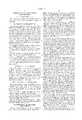
- FIG. 1illustrates an energy band diagram at a normal interface of indium arsenide and gallium arsenide
- FIG. 2illustrates an energy band diagram at an interface of indium arsenide changed gradually to gallium arsenide using indium gallium arsenide
- FIG. 3illustrates an energy band diagram at a silicon doped interface of indium arsenide and gallium arsenide, in accordance with the present invention.
- the present inventionprovides, among other things, an ohmic contact, a method of fabricating an ohmic contact, a method of improving contact resistance in a multi-layer heterostructure, and a method of introducing continuity at an interface of indium arsenide and gallium arsenide in an ohmic contact.
- the present inventionis easy to implement, efficient and exemplary for facilitating good contact resistance to allow electron tunneling.
- FIG. 1illustrates an energy band diagram, including a conduction band 10 and valence band 11, of a structure 12 with an interface 13 of an indium arsenide (InAs) layer 14 and a gallium arsenide (GaAs) substrate 15. Further shown is a barrier 16 for carriers at interface 13. Barrier 16 prevents good ohmic contact at interface 13 thus inhibiting tunneling along path 17 traversing barrier 16 from InAs 14 to GaAs 15, an anomaly commonly referred to be a result of Fermi level pinning. For the purposes of orientation, path 17 substantially defines the Fermi level.
- InAsindium arsenide
- GaAsgallium arsenide
- FIG. 2illustrates an energy band diagram, including a conduction band 20 and a valence band 21, of a structure 22 with an interface 23 of an InAs layer 24 and a GaAs substrate 25 using indium gallium arsenide (InGaAs) 26.
- InGaAsindium gallium arsenide
- FIG. 2illustrates an energy band diagram, including a conduction band 20 and a valence band 21, of a structure 22 with an interface 23 of an InAs layer 24 and a GaAs substrate 25 using indium gallium arsenide (InGaAs) 26.
- InGaAsindium gallium arsenide
- FIG. 3illustrates an energy band diagram, including a conduction band 30 and a valence band 31, of a structure 32 with a multiple silicon delta doped interface 33 of an InAs layer 34 and a GaAs substrate 35, in accordance with the present invention.
- delta doping very close to interface 33 with n-siliconeliminates or otherwise substantially reduces the formation of a barrier and therefore eliminates Fermi level pinning thus providing for a good quality ohmic contact and wide continuity at interface 33.
- a single delta doping close to interface 33will reduce the barrier, generally a plurality of delta dopings, illustrated as notches 38 in FIG. 3, provide a more satisfactory interface match.
- the delta doping farthest from interface 33will generally be within approximately 1000 ⁇ from interface 33, since delta dopings farther than that have little effect, and the delta doping nearest to interface 33 will generally be within approximately 20 ⁇ to 30 ⁇ from interface 33.
- the delta doping closest to interface 33should be as close as possible without being exposed by subsequent process steps, e.g. the formation of layer 34.
- Structure 32operative as a non-alloyed ohmic contact, can be used to make single step metalization processes for forming, in addition, a gate contact to the GaAs devices.
- multiple delta-doped n-silicon close to interface 33 of InAs layer 34 and GaAs layer 35provides for wide continuity at interface 33 and prevents formation of a wide barrier at the pinned GaAs/InAs interface thus allowing tunneling due to an effective decrease in barrier height and a narrowing of the depletion region.
- very good contact resistance 3-4 E-7 ohm-cm 2is possible, Fermi level pinning at the interface is substantially eliminated, the formation of non-alloyed ohmic contacts is possible, and the process can easily be incorporated in epitaxial growth, such as by molecular/chemical beam epitaxy, while eliminating the need to grow compositionally graded InGaAs.
- delta doping n-siliconhas not been herein discussed in great detail, such doping techniques and details are disclosed in exemplary detail in Si Atomic-Planar-Doping in GaAs Made by Molecular Beam Epitaxy, JAPANESE JOURNAL OF APPLIED PHYSICS, Vol. 24, No. 8, August, 1985, pp. L602-L604, of which is incorporated herein by reference.
Landscapes
- Engineering & Computer Science (AREA)
- Physics & Mathematics (AREA)
- Condensed Matter Physics & Semiconductors (AREA)
- General Physics & Mathematics (AREA)
- Manufacturing & Machinery (AREA)
- Computer Hardware Design (AREA)
- Microelectronics & Electronic Packaging (AREA)
- Power Engineering (AREA)
- Junction Field-Effect Transistors (AREA)
- Electrodes Of Semiconductors (AREA)
Abstract
Description
Claims (14)
Priority Applications (2)
| Application Number | Priority Date | Filing Date | Title |
|---|---|---|---|
| US09/072,197US6043143A (en) | 1998-05-04 | 1998-05-04 | Ohmic contact and method of manufacture |
| US09/502,702US6172420B1 (en) | 1998-05-04 | 2000-02-11 | Silicon delta-doped gallium arsenide/indium arsenide heterojunction OHMIC contact |
Applications Claiming Priority (1)
| Application Number | Priority Date | Filing Date | Title |
|---|---|---|---|
| US09/072,197US6043143A (en) | 1998-05-04 | 1998-05-04 | Ohmic contact and method of manufacture |
Related Child Applications (1)
| Application Number | Title | Priority Date | Filing Date |
|---|---|---|---|
| US09/502,702DivisionUS6172420B1 (en) | 1998-05-04 | 2000-02-11 | Silicon delta-doped gallium arsenide/indium arsenide heterojunction OHMIC contact |
Publications (1)
| Publication Number | Publication Date |
|---|---|
| US6043143Atrue US6043143A (en) | 2000-03-28 |
Family
ID=22106170
Family Applications (2)
| Application Number | Title | Priority Date | Filing Date |
|---|---|---|---|
| US09/072,197Expired - Fee RelatedUS6043143A (en) | 1998-05-04 | 1998-05-04 | Ohmic contact and method of manufacture |
| US09/502,702Expired - Fee RelatedUS6172420B1 (en) | 1998-05-04 | 2000-02-11 | Silicon delta-doped gallium arsenide/indium arsenide heterojunction OHMIC contact |
Family Applications After (1)
| Application Number | Title | Priority Date | Filing Date |
|---|---|---|---|
| US09/502,702Expired - Fee RelatedUS6172420B1 (en) | 1998-05-04 | 2000-02-11 | Silicon delta-doped gallium arsenide/indium arsenide heterojunction OHMIC contact |
Country Status (1)
| Country | Link |
|---|---|
| US (2) | US6043143A (en) |
Cited By (1)
| Publication number | Priority date | Publication date | Assignee | Title |
|---|---|---|---|---|
| US20080017891A1 (en)* | 2006-06-30 | 2008-01-24 | Suman Datta | Pinning layer for low resistivity n-type source drain ohmic contacts |
Families Citing this family (3)
| Publication number | Priority date | Publication date | Assignee | Title |
|---|---|---|---|---|
| US6670653B1 (en)* | 1999-07-30 | 2003-12-30 | Hrl Laboratories, Llc | InP collector InGaAsSb base DHBT device and method of forming same |
| WO2007062327A2 (en)* | 2005-11-18 | 2007-05-31 | Ideal Industries, Inc. | Releasable wire connector |
| US9530708B1 (en) | 2013-05-31 | 2016-12-27 | Hrl Laboratories, Llc | Flexible electronic circuit and method for manufacturing same |
Family Cites Families (8)
| Publication number | Priority date | Publication date | Assignee | Title |
|---|---|---|---|---|
| JPH0783028B2 (en)* | 1986-06-02 | 1995-09-06 | 株式会社日立製作所 | Semiconductor device and manufacturing method |
| US4772934A (en)* | 1986-06-06 | 1988-09-20 | American Telephone And Telegraph Company, At&T Bell Laboratories | Delta-doped ohmic metal to semiconductor contacts |
| US4780748A (en)* | 1986-06-06 | 1988-10-25 | American Telephone & Telegraph Company, At&T Bell Laboratories | Field-effect transistor having a delta-doped ohmic contact |
| US5098859A (en)* | 1986-06-19 | 1992-03-24 | International Business Machines Corporation | Method for forming distributed barrier compound semiconductor contacts |
| US4784967A (en)* | 1986-12-19 | 1988-11-15 | American Telephone And Telegraph Company, At&T Bell Laboratories | Method for fabricating a field-effect transistor with a self-aligned gate |
| US5013685A (en)* | 1989-11-02 | 1991-05-07 | At&T Bell Laboratories | Method of making a non-alloyed ohmic contact to III-V semiconductors-on-silicon |
| JPH05304290A (en)* | 1992-04-28 | 1993-11-16 | Nec Corp | Ohmic electrode |
| US5268582A (en)* | 1992-08-24 | 1993-12-07 | At&T Bell Laboratories | P-N junction devices with group IV element-doped group III-V compound semiconductors |
- 1998
- 1998-05-04USUS09/072,197patent/US6043143A/ennot_activeExpired - Fee Related
- 2000
- 2000-02-11USUS09/502,702patent/US6172420B1/ennot_activeExpired - Fee Related
Cited By (2)
| Publication number | Priority date | Publication date | Assignee | Title |
|---|---|---|---|---|
| US20080017891A1 (en)* | 2006-06-30 | 2008-01-24 | Suman Datta | Pinning layer for low resistivity n-type source drain ohmic contacts |
| US7355254B2 (en)* | 2006-06-30 | 2008-04-08 | Intel Corporation | Pinning layer for low resistivity N-type source drain ohmic contacts |
Also Published As
| Publication number | Publication date |
|---|---|
| US6172420B1 (en) | 2001-01-09 |
Similar Documents
| Publication | Publication Date | Title |
|---|---|---|
| EP0447327B1 (en) | Heterostructure semiconductor device | |
| EP0619613B1 (en) | A heterojunction bipolar transistor | |
| EP0568050B1 (en) | Ohmic contact on a compound semiconductor layer | |
| US5837565A (en) | Semiconductor device | |
| EP0381396A1 (en) | Compound semiconductor devices | |
| KR19980034078A (en) | Hot Electron Device and Resonant Tunneling Hot Electronic Device | |
| US5952672A (en) | Semiconductor device and method for fabricating the same | |
| EP0051271A1 (en) | Heterojunction semiconductor device | |
| KR920003799B1 (en) | Semiconductor device | |
| US20040169194A1 (en) | Semiconductor device | |
| US5351128A (en) | Semiconductor device having reduced contact resistance between a channel or base layer and a contact layer | |
| US5322808A (en) | Method of fabricating inverted modulation-doped heterostructure | |
| US5981986A (en) | Semiconductor device having a heterojunction | |
| US6043143A (en) | Ohmic contact and method of manufacture | |
| US5381027A (en) | Semiconductor device having a heterojunction and a two dimensional gas as an active layer | |
| US5258631A (en) | Semiconductor device having a two-dimensional electron gas as an active layer | |
| KR100548047B1 (en) | Field Effect Transistor | |
| JP2703885B2 (en) | Semiconductor device | |
| JPH0260225B2 (en) | ||
| JP3255973B2 (en) | Semiconductor device | |
| JP2708492B2 (en) | Method for manufacturing semiconductor device | |
| JPS6012773A (en) | Method for manufacturing semiconductor devices | |
| JP2980630B2 (en) | Compound semiconductor device | |
| JP2800457B2 (en) | Semiconductor device | |
| JPH0468775B2 (en) |
Legal Events
| Date | Code | Title | Description |
|---|---|---|---|
| AS | Assignment | Owner name:MOTOROLA, INC., ILLINOIS Free format text:ASSIGNMENT OF ASSIGNORS INTEREST;ASSIGNOR:SHIRALAGI, KUMAR;REEL/FRAME:009215/0549 Effective date:19980427 | |
| FPAY | Fee payment | Year of fee payment:4 | |
| AS | Assignment | Owner name:FREESCALE SEMICONDUCTOR, INC., TEXAS Free format text:ASSIGNMENT OF ASSIGNORS INTEREST;ASSIGNOR:MOTOROLA, INC.;REEL/FRAME:015698/0657 Effective date:20040404 Owner name:FREESCALE SEMICONDUCTOR, INC.,TEXAS Free format text:ASSIGNMENT OF ASSIGNORS INTEREST;ASSIGNOR:MOTOROLA, INC.;REEL/FRAME:015698/0657 Effective date:20040404 | |
| AS | Assignment | Owner name:CITIBANK, N.A. AS COLLATERAL AGENT, NEW YORK Free format text:SECURITY AGREEMENT;ASSIGNORS:FREESCALE SEMICONDUCTOR, INC.;FREESCALE ACQUISITION CORPORATION;FREESCALE ACQUISITION HOLDINGS CORP.;AND OTHERS;REEL/FRAME:018855/0129 Effective date:20061201 Owner name:CITIBANK, N.A. AS COLLATERAL AGENT,NEW YORK Free format text:SECURITY AGREEMENT;ASSIGNORS:FREESCALE SEMICONDUCTOR, INC.;FREESCALE ACQUISITION CORPORATION;FREESCALE ACQUISITION HOLDINGS CORP.;AND OTHERS;REEL/FRAME:018855/0129 Effective date:20061201 | |
| FPAY | Fee payment | Year of fee payment:8 | |
| AS | Assignment | Owner name:CITIBANK, N.A., AS COLLATERAL AGENT,NEW YORK Free format text:SECURITY AGREEMENT;ASSIGNOR:FREESCALE SEMICONDUCTOR, INC.;REEL/FRAME:024397/0001 Effective date:20100413 Owner name:CITIBANK, N.A., AS COLLATERAL AGENT, NEW YORK Free format text:SECURITY AGREEMENT;ASSIGNOR:FREESCALE SEMICONDUCTOR, INC.;REEL/FRAME:024397/0001 Effective date:20100413 | |
| REMI | Maintenance fee reminder mailed | ||
| LAPS | Lapse for failure to pay maintenance fees | ||
| STCH | Information on status: patent discontinuation | Free format text:PATENT EXPIRED DUE TO NONPAYMENT OF MAINTENANCE FEES UNDER 37 CFR 1.362 | |
| FP | Lapsed due to failure to pay maintenance fee | Effective date:20120328 | |
| AS | Assignment | Owner name:FREESCALE SEMICONDUCTOR, INC., TEXAS Free format text:PATENT RELEASE;ASSIGNOR:CITIBANK, N.A., AS COLLATERAL AGENT;REEL/FRAME:037354/0225 Effective date:20151207 Owner name:FREESCALE SEMICONDUCTOR, INC., TEXAS Free format text:PATENT RELEASE;ASSIGNOR:CITIBANK, N.A., AS COLLATERAL AGENT;REEL/FRAME:037356/0553 Effective date:20151207 Owner name:FREESCALE SEMICONDUCTOR, INC., TEXAS Free format text:PATENT RELEASE;ASSIGNOR:CITIBANK, N.A., AS COLLATERAL AGENT;REEL/FRAME:037356/0143 Effective date:20151207 |