US6042975A - Alignment techniques for photolithography utilizing multiple photoresist layers - Google Patents
Alignment techniques for photolithography utilizing multiple photoresist layersDownload PDFInfo
- Publication number
- US6042975A US6042975AUS09/111,534US11153498AUS6042975AUS 6042975 AUS6042975 AUS 6042975AUS 11153498 AUS11153498 AUS 11153498AUS 6042975 AUS6042975 AUS 6042975A
- Authority
- US
- United States
- Prior art keywords
- layer
- photoresist
- photomask
- gate
- photoresist layer
- Prior art date
- Legal status (The legal status is an assumption and is not a legal conclusion. Google has not performed a legal analysis and makes no representation as to the accuracy of the status listed.)
- Expired - Lifetime
Links
- 238000000034methodMethods0.000titleclaimsabstractdescription33
- 229920002120photoresistant polymerPolymers0.000titleclaimsdescription58
- 238000000206photolithographyMethods0.000titleabstractdescription7
- 239000000758substrateSubstances0.000claimsdescription15
- 238000004519manufacturing processMethods0.000claimsdescription12
- 239000004065semiconductorSubstances0.000claimsdescription10
- 230000005855radiationEffects0.000claimsdescription8
- 238000000151depositionMethods0.000claimsdescription4
- 230000008569processEffects0.000abstractdescription21
- 239000010410layerSubstances0.000description57
- 239000002184metalSubstances0.000description16
- 229910052751metalInorganic materials0.000description16
- 235000012431wafersNutrition0.000description13
- 229910001218Gallium arsenideInorganic materials0.000description6
- 238000001704evaporationMethods0.000description6
- 230000008020evaporationEffects0.000description5
- 238000001459lithographyMethods0.000description5
- 238000002508contact lithographyMethods0.000description4
- 239000010931goldSubstances0.000description4
- 229910052737goldInorganic materials0.000description4
- 238000012545processingMethods0.000description4
- 239000010936titaniumSubstances0.000description4
- 238000000576coating methodMethods0.000description3
- 238000000609electron-beam lithographyMethods0.000description3
- 238000001465metallisationMethods0.000description3
- BASFCYQUMIYNBI-UHFFFAOYSA-NplatinumSubstances[Pt]BASFCYQUMIYNBI-UHFFFAOYSA-N0.000description3
- 239000010703siliconSubstances0.000description3
- 229910052710siliconInorganic materials0.000description3
- 239000002356single layerSubstances0.000description3
- 229910052719titaniumInorganic materials0.000description3
- CSCPPACGZOOCGX-UHFFFAOYSA-NAcetoneChemical compoundCC(C)=OCSCPPACGZOOCGX-UHFFFAOYSA-N0.000description2
- 229910000980Aluminium gallium arsenideInorganic materials0.000description2
- IJGRMHOSHXDMSA-UHFFFAOYSA-NAtomic nitrogenChemical compoundN#NIJGRMHOSHXDMSA-UHFFFAOYSA-N0.000description2
- XUIMIQQOPSSXEZ-UHFFFAOYSA-NSiliconChemical compound[Si]XUIMIQQOPSSXEZ-UHFFFAOYSA-N0.000description2
- 238000013459approachMethods0.000description2
- 238000000231atomic layer depositionMethods0.000description2
- 239000000969carrierSubstances0.000description2
- 238000005229chemical vapour depositionMethods0.000description2
- 239000011248coating agentSubstances0.000description2
- 238000005516engineering processMethods0.000description2
- 230000005669field effectEffects0.000description2
- 239000000463materialSubstances0.000description2
- 239000011159matrix materialSubstances0.000description2
- 229910000530Gallium indium arsenideInorganic materials0.000description1
- RTAQQCXQSZGOHL-UHFFFAOYSA-NTitaniumChemical compound[Ti]RTAQQCXQSZGOHL-UHFFFAOYSA-N0.000description1
- 238000001015X-ray lithographyMethods0.000description1
- QVGXLLKOCUKJST-UHFFFAOYSA-Natomic oxygenChemical compound[O]QVGXLLKOCUKJST-UHFFFAOYSA-N0.000description1
- 230000004888barrier functionEffects0.000description1
- 230000008901benefitEffects0.000description1
- 230000015572biosynthetic processEffects0.000description1
- 230000015556catabolic processEffects0.000description1
- 238000004140cleaningMethods0.000description1
- 238000010586diagramMethods0.000description1
- 230000000694effectsEffects0.000description1
- 238000005530etchingMethods0.000description1
- PCHJSUWPFVWCPO-UHFFFAOYSA-NgoldChemical compound[Au]PCHJSUWPFVWCPO-UHFFFAOYSA-N0.000description1
- 239000004615ingredientSubstances0.000description1
- 230000010354integrationEffects0.000description1
- 239000002346layers by functionSubstances0.000description1
- 239000007769metal materialSubstances0.000description1
- 238000012986modificationMethods0.000description1
- 230000004048modificationEffects0.000description1
- 238000001451molecular beam epitaxyMethods0.000description1
- 229910052757nitrogenInorganic materials0.000description1
- 239000001301oxygenSubstances0.000description1
- 229910052760oxygenInorganic materials0.000description1
- 238000000059patterningMethods0.000description1
- 229910052697platinumInorganic materials0.000description1
- 230000004044responseEffects0.000description1
- 238000000926separation methodMethods0.000description1
- 239000002904solventSubstances0.000description1
- 125000006850spacer groupChemical group0.000description1
- 238000009987spinningMethods0.000description1
- 238000004544sputter depositionMethods0.000description1
- 238000010561standard procedureMethods0.000description1
- 239000002344surface layerSubstances0.000description1
- 238000012876topographyMethods0.000description1
- XLYOFNOQVPJJNP-UHFFFAOYSA-NwaterSubstancesOXLYOFNOQVPJJNP-UHFFFAOYSA-N0.000description1
- 238000001039wet etchingMethods0.000description1
Images


Classifications
- H—ELECTRICITY
- H10—SEMICONDUCTOR DEVICES; ELECTRIC SOLID-STATE DEVICES NOT OTHERWISE PROVIDED FOR
- H10D—INORGANIC ELECTRIC SEMICONDUCTOR DEVICES
- H10D30/00—Field-effect transistors [FET]
- H10D30/01—Manufacture or treatment
- H10D30/015—Manufacture or treatment of FETs having heterojunction interface channels or heterojunction gate electrodes, e.g. HEMT
- G—PHYSICS
- G03—PHOTOGRAPHY; CINEMATOGRAPHY; ANALOGOUS TECHNIQUES USING WAVES OTHER THAN OPTICAL WAVES; ELECTROGRAPHY; HOLOGRAPHY
- G03F—PHOTOMECHANICAL PRODUCTION OF TEXTURED OR PATTERNED SURFACES, e.g. FOR PRINTING, FOR PROCESSING OF SEMICONDUCTOR DEVICES; MATERIALS THEREFOR; ORIGINALS THEREFOR; APPARATUS SPECIALLY ADAPTED THEREFOR
- G03F9/00—Registration or positioning of originals, masks, frames, photographic sheets or textured or patterned surfaces, e.g. automatically
- G03F9/70—Registration or positioning of originals, masks, frames, photographic sheets or textured or patterned surfaces, e.g. automatically for microlithography
- G03F9/7073—Alignment marks and their environment
- G03F9/708—Mark formation
- G—PHYSICS
- G03—PHOTOGRAPHY; CINEMATOGRAPHY; ANALOGOUS TECHNIQUES USING WAVES OTHER THAN OPTICAL WAVES; ELECTROGRAPHY; HOLOGRAPHY
- G03F—PHOTOMECHANICAL PRODUCTION OF TEXTURED OR PATTERNED SURFACES, e.g. FOR PRINTING, FOR PROCESSING OF SEMICONDUCTOR DEVICES; MATERIALS THEREFOR; ORIGINALS THEREFOR; APPARATUS SPECIALLY ADAPTED THEREFOR
- G03F9/00—Registration or positioning of originals, masks, frames, photographic sheets or textured or patterned surfaces, e.g. automatically
- G03F9/70—Registration or positioning of originals, masks, frames, photographic sheets or textured or patterned surfaces, e.g. automatically for microlithography
- G03F9/7073—Alignment marks and their environment
- G03F9/7084—Position of mark on substrate, i.e. position in (x, y, z) of mark, e.g. buried or resist covered mark, mark on rearside, at the substrate edge, in the circuit area, latent image mark, marks in plural levels
- H—ELECTRICITY
- H01—ELECTRIC ELEMENTS
- H01L—SEMICONDUCTOR DEVICES NOT COVERED BY CLASS H10
- H01L21/00—Processes or apparatus adapted for the manufacture or treatment of semiconductor or solid state devices or of parts thereof
- H01L21/02—Manufacture or treatment of semiconductor devices or of parts thereof
- H01L21/027—Making masks on semiconductor bodies for further photolithographic processing not provided for in group H01L21/18 or H01L21/34
- H01L21/0271—Making masks on semiconductor bodies for further photolithographic processing not provided for in group H01L21/18 or H01L21/34 comprising organic layers
- H01L21/0273—Making masks on semiconductor bodies for further photolithographic processing not provided for in group H01L21/18 or H01L21/34 comprising organic layers characterised by the treatment of photoresist layers
- H01L21/0274—Photolithographic processes
- H—ELECTRICITY
- H01—ELECTRIC ELEMENTS
- H01L—SEMICONDUCTOR DEVICES NOT COVERED BY CLASS H10
- H01L21/00—Processes or apparatus adapted for the manufacture or treatment of semiconductor or solid state devices or of parts thereof
- H01L21/02—Manufacture or treatment of semiconductor devices or of parts thereof
- H01L21/04—Manufacture or treatment of semiconductor devices or of parts thereof the devices having potential barriers, e.g. a PN junction, depletion layer or carrier concentration layer
- H01L21/18—Manufacture or treatment of semiconductor devices or of parts thereof the devices having potential barriers, e.g. a PN junction, depletion layer or carrier concentration layer the devices having semiconductor bodies comprising elements of Group IV of the Periodic Table or AIIIBV compounds with or without impurities, e.g. doping materials
- H01L21/28—Manufacture of electrodes on semiconductor bodies using processes or apparatus not provided for in groups H01L21/20 - H01L21/268
- H01L21/283—Deposition of conductive or insulating materials for electrodes conducting electric current
- H01L21/285—Deposition of conductive or insulating materials for electrodes conducting electric current from a gas or vapour, e.g. condensation
- H01L21/28506—Deposition of conductive or insulating materials for electrodes conducting electric current from a gas or vapour, e.g. condensation of conductive layers
- H01L21/28575—Deposition of conductive or insulating materials for electrodes conducting electric current from a gas or vapour, e.g. condensation of conductive layers on semiconductor bodies comprising AIIIBV compounds
- H01L21/28587—Deposition of conductive or insulating materials for electrodes conducting electric current from a gas or vapour, e.g. condensation of conductive layers on semiconductor bodies comprising AIIIBV compounds characterised by the sectional shape, e.g. T, inverted T
Definitions
- This inventionrelates to lithography techniques used in the manufacture of electronic and photonic integrated circuits.
- lithographyis a key technology in fabricating wafers with large number of chip sites.
- x-ray and electron beam lithography toolsare useful and effective, especially for mask making, photolithography remains the most widely used lithography tool for semiconductor wafer fabrication.
- step and repeat camerasare essentially ubiquitous in commercial integrated circuit manufacture. These tools, usually referred to as steppers, rely for their effectiveness on the ability to register photomasks in exact alignment from level to level.
- Typical state of the art wafer fabrication processeshave several levels or layers where photomasks are employed in conjunction with standard process steps to define features in the device substrate or on the layers.
- alignment markare formed on the first level to provide means for registering the photomask for the subsequent photolithography step.
- the marksusually consist of an etched pattern formed by photolithography.
- Photolithographic patternsare typically made by spinning a uniform coating of photoresist over the entire wafer, exposing the photoresist with actinic light directed through a photomask, and developing the photoresist to leave a photoresist pattern.
- photomaskrefers to the master mask or reticle that defines the pattern of actinic radiation incident on the photoresist.
- lithographic maskrefers to the patterned photoresist which is used to define the regions where processing activity, e.g. etching, occurs in the layer masked by the photoresist.
- Each photomask, and the photoresist pattern produced therefromtypically has imbedded therein a series of alignment marks, which are key ingredients in multilevel wafer fabrication. For example, if the first photoresist pattern is used to mask an oxide layer, silicon layer, or a metal layer for an etch step, the alignment marks will be transferred to the layer as an etched pattern.
- the alignment marks from the first layercan be used to register all succeeding photomasks.
- the desired topographycan be constructed with great precision in the x-y planes.
- the alignment itselfis usually performed with automated tools.
- State of the art steppershave vision systems that easily identify the alignment marks on the wafer and automatically register the next photomask with the alignment marks previously formed.
- the single level of photoresistmay comprise one or more photoresist layers.
- the multiple photomask exposuresare made sequentially, and the multiple patterns are developed simultaneously.
- a key feature in the multiple exposureis the use of latent alignment marks formed in the photoresist after the first photomask exposure but before the photoresist is developed. It has been found that these marks, while difficult to resolve by human vision, are visible and recognizable by the laser alignment tool of the stepper apparatus. Subsequent reticles in the multiple exposure are aligned to these marks.
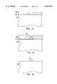
- FIGS. 1 and 2are schematic diagrams of a lift-off process for patterning a metal layer in the manufacture of semiconductor devices
- FIGS. 3-5represent steps in a multiple exposure photolithographic process for making a lift-off mask according to the invention
- FIG. 6is a schematic representation of a recessed gate MESFET device with a T-shaped Schottky gate that may be fabricated in accordance with the invention
- FIG. 7is a schematic view of a T-shaped gate structure describing the relevant dimensions discussed in this description.
- FIG. 8is a schematic representation of a HEMT device with a T-shaped gate that may be fabricated in accordance with the invention.
- FIGS. 9-15represent steps in a multiple exposure photolithographic process according to the invention for forming T-gate structures.
- a portion of a semiconductor substrate 11is shown with lift-off mask 12.
- the lift-off maskis typically photoresist and can be formed by a single layer, or by multiple layers as shown.
- the objectiveis to develop a significant undercut 13 in the layer so that when the metal layer is deposited there is sufficient physical discontinuity to discourage metal stringers between the metal 14 in the window and the metal 15 on the lift-off mask 12.
- the structure after lift-offis shown in FIG. 2.
- FIGS. 3-5A process according to the invention for forming the lift-off mask with the desired undercut will be described in conjunction with FIGS. 3-5.
- the semiconductor substrate 21is shown with a photoresist layer 22.
- the substrates used to demonstrate the inventionconsisted of 2" diameter, 25 mil thick wafers of (100) Si, GaAs, and InP.
- the photoresistwas Shipley 1818 spun at 3000 RPM, and baked on a hot plate at 110° C. for 60 sec, resulting in a resist thickness of 2.1 ⁇ m.
- the resist coated waferswere exposed in a Nikon NSR 1505G6E stepper. Exposure wavelength was 436 nm.
- Exposure dose and depth of focus, or focus offset from the substrate-resist interfacewere optimized using a focus/expose matrix of (0 ⁇ m to -1.0 ⁇ m)/(600 mjoules to 1400 mjoules) in steps of 0.25 ⁇ m and/or 100 mjoules.
- a focus/expose matrixof (0 ⁇ m to -1.0 ⁇ m)/(600 mjoules to 1400 mjoules) in steps of 0.25 ⁇ m and/or 100 mjoules.
- approximately half the thickness of the resist layer 22was exposed using the first photomask 23.
- UV radiationis represented in FIG. 3 by arrows 25, and the exposed region of the photoresist layer is shown at 26.
- the alignment marks in photomask 26are represented schematically at 27, and are located typically at an appropriate edge or corner of each integrated circuit pattern.
- the alignment marks 27are transferred to photoresist layer 22 as a latent image and remain there for the second photomask alignment and exposure, shown in FIG. 4.
- the second photomask 41with a mask opening smaller than the opening of the first photomask (FIG. 3), is shown with actinic radiation indicated at 43. This step exposes portion 44 of resist layer 22.
- the second photomaskis aligned by registering alignment marks on the photomask 42, to the latent alignment marks 27 already formed in photoresist layer 22.
- the exposed portions 26 and 44 of photoresist layer 22are then developed and dissolved away by standard procedures, leaving the photoresist pattern shown in FIG. 5, with the pronounced undercut 51 in the opening as desired.
- the photomaskis shown schematically and appears positioned close to the surface of the photoresist layer as it would be in a contact printing process. However, as will be evident to those skilled in the art, in a stepper the photomask will normally be projected onto the photoresist surface by the step and repeat camera.
- the inventioncan also be used with contact printing lithography.
- the alignment marksare visible to the stepper equipment, but are only marginally visible to human operators frequently used in contact printing.
- contact printing using human operator alignmentcan be performed with the aid of a contrast enhancement layer.
- CEM BC 5a known barrier coating, can be spun on the photoresist layer, followed by the application of a known contrast enhancement material, CEM 420 WS.
- the T-shaped electrodes for these devicesare produced by exposing T-shaped patterns in the resist at the gate location, developing the resist to form T-shaped openings, and evaporating metal into the T-shaped openings. A lift-off process is used to remove excess metal on the resist surface between T-shaped features.
- the T-shaped patternsare formed by e-beam lithography.
- T-shaped Schottky gate structures for use in III-V field effect transistor devicescan be made with a convenient and cost-effective photolithographic process. Multiple exposure of a thick photoresist layer is used to define T-shaped features, and gate contact metal is deposited in the T-shaped features to form the T-gate structure.
- a MESFET deviceis shown with substrate 61, typically semi-insulating GaAs, and active layer 62, which is implanted with n-silicon n-type carriers.
- the cap layer 63 for the source/drain contactsis silicon implanted n + .
- the source and drain contacts 64 and 65are conventional metal materials such as Ti/Pd/Au, Ti/Pt/Au, Al/Ti, Au/Ge.
- the gateis recessed by wet etching a window in layer 63 so that the gate is situated on the active layer 62.
- MESFET devicesare typically depletion mode devices with Schottky gates which, in contrast with Si MOS transistors, are "normally on" devices.
- the T-shaped Schottky gate for the MESFET device in FIG. 6is shown at 67, and is made of a conventional contact metal.
- n-type carriersare depleted from depletion region 68 beneath the Schottky gate leaving a p-region that pinches off current flow between the source and drain.
- the gate 67is referred to as T-shaped but is not to be confused with gate configurations, known in the art, that are T-shaped in plan view.
- the gate configuration in FIG. 6, and which describes the objective of this embodiment of the invention,is a vertical T-shape. It can be defined as having a vertical base 71 and a "cross" 72.
- the shape of the gate in a plan viewmay be square but is conventionally rectangular in shape with the width ⁇ of the gate extending into the plane of the figure and typically terminating in a contact pad (not shown) outside the active region of the device.
- Enhancement of the gate conductivityis a function of the increased cross section between the extremities of the gate along the conduction path.
- the objective in these devicesis to minimize the gate length l which is the device parameter controlling the frequency response of the transistor.
- the gate resistance along the gate width wincreases proportionately.
- the normal gate cross sectionis l 1 ⁇ h 1
- the enhanced cross sectionis (h 2 ⁇ l 2 )-h 1 (l 2 -l 1 ).
- HEMT devicescan also take advantage of the enhanced conductivity of T-shaped gates.
- a HEMT deviceis shown in FIG. 8. These devices are similar in appearance to the MESFET of FIG. 6 but are more complex in the internal structure and are designed for lower noise, higher frequency performance, and in special structures, higher power.
- the source and drain contacts 73 and 74are typically formed on an n + GaAs layer 75 but the Schottky gate in this structure contacts a heterostructure layer 76, e.g. AlGaAs, under contact layer 75.
- the active layer 76 and the depletion region 77are otherwise similar to corresponding elements in the MESFET.
- Layer 78is a very thin spacer layer of e.g.
- the substrate 81may be semi-insulating GaAs.
- the T-shaped Schottky gate structureis shown at 82 and is essentially the same as in the MESFET device of FIG. 6.
- FIGS. 9-15The technique for fabricating the T-shaped gate structures according to the invention will be described in conjunction with FIGS. 9-15.
- the functional layers in the substratewill be omitted, the assumption being that these device features are complete at the point in the process where gate fabrication commences.
- the region of the device being processed in FIGS. 9-15is the substrate surface between the source and drain electrodes.
- the substrate 84is coated with a first level of photoresist 85.
- the choice of photoresist for these layersis not critical and can be any conventional resist material, either positive or negative.
- Shipley 1805 photoresistmay be spun on the wafer at 3000 rpm for 30 seconds to produce a photoresist layer of 0.5 ⁇ m in thickness, and the layer prebaked on a hotplate at 110° C. for 60 seconds.
- the thickness of the first level of photoresistcorresponds to dimension h 1 of FIG. 7, and is preferably in the range 0.2-2.0 ⁇ m.
- the photoresist layer 85is exposed to actinic radiation 86 through a first photomask 87 using standard practice as shown in FIG. 10.
- a latent image of the alignment marks 88is formed in layer 85.
- the second photoresist layer 89is spun on over the photoresist layer 85 as shown in FIG. 11.
- the thickness of the second level photoresist layer 89corresponds to dimension h 2 of FIG. 7 with excess height added to accommodate the liftoff process as will be described below.
- the thicknesswill typically be in the range 0.3-3.0 ⁇ m.
- Shipley 1818may be used for the second level photoresist, and e.g. spun at 3000 rpm for 30 seconds giving a photoresist layer thickness of 1.8 ⁇ m.
- the layeris prebaked on a hotplate at 110° C. for 60 seconds.
- the second photoresist layer 89is exposed using photomask 91 and aligning the alignment marks 92 of photomask 91 with the latent alignment marks 88 in photoresist layer 85. These marks are visible to the automated alignment system of the stepper through the transparent resist layer 91.
- the opening in photomask 91corresponds to the cross portion 72 of the "T" as shown in FIGS. 6-8.
- the exposure time for the Nikon stepper to expose to the bottom of the second photoresist levelwas 1200 milliseconds.
- the two levels of photoresistare developed in Shipley 321 developer and rinsed in D.I. water for 30 seconds.
- the resulting structureshown in FIG. 13, is then ready for metallization to form the T-shaped gate.
- the T-shaped exposure patterncan also be formed using a single layer of photoresist as in the earlier example. Multiple exposures are used while varying the depth of focus, and mixing between the two resist layers is avoided.
- the deposition technique used to deposit the metal, and the composition of the metalare subject to a variety of choices known to those in the art. Evaporation is preferred because it is relatively directional, and therefore is well suited for lift-off processes. Sputtering may also be used. Conformal coating processes such as Chemical Vapor Deposition (CVD), Molecular Beam Epitaxy (MBE) and Atomic Layer Deposition (ALD), are less likely to be effective but ways may be devised by those skilled in the art to adapt these techniques to the process described. In the specific example described here, the preferred deposition technique is evaporation using an e-beam evaporation process.
- CVDChemical Vapor Deposition
- MBEMolecular Beam Epitaxy
- ALDAtomic Layer Deposition
- the substratePrior to evaporation the substrate may be exposed to a pre-deposit cleaning operation for 3 minutes in an oxygen plasma at 50 watts and 250 mTorr, followed by a 10:1 HCl:H 2 O rinse for 30 seconds. The surface is blow dried with nitrogen for 30 seconds.
- the two levels of resist 85 and 89, carrying the surface layer of unwanted metal 94are then dissolved in a solvent such as acetone, leaving the final T-shaped gate 97 as shown in FIG. 15.
- the image of the alignment marks formed in the first photoresist layeris referred to as a "latent" image. This refers to an image that is discernible by some means even though it may be only marginally visible to the human eye.
- the operation of the photolithography apparatusnormally involves an alignment step and an exposure step.
- the reticleis registered to the alignment pattern on the substrate using the laser alignment system, and the appropriate UV exposure is made.
- the reticleis stepped to the next site, and the operation is repeated.
- In the first exposure of the wafer fabrication sequencethere is no alignment pattern on the substrate.
- the invention described abovewill be most useful when the multiple exposure is used as the first photolithographic operation in the wafer fabrication sequence, i.e. when there are no alignment patterns present on the substrate. Thereafter, alignment patterns will typically be available for multiple alignments to those patterns.
- the embodiment of the invention in which multiple exposures are made in a single photoresist layerrelies on the ability to expose the layer at different thickness levels. This can easily be implemented using the spatial focusing matrix described earlier. Other techniques may be found for reaching the same result. Bi-level resist and tri-level resist schemes can be used. Resist levels having different actinic properties can be used, as well as different exposure wavelengths.
Landscapes
- Physics & Mathematics (AREA)
- General Physics & Mathematics (AREA)
- Engineering & Computer Science (AREA)
- Condensed Matter Physics & Semiconductors (AREA)
- Manufacturing & Machinery (AREA)
- Computer Hardware Design (AREA)
- Microelectronics & Electronic Packaging (AREA)
- Power Engineering (AREA)
- Junction Field-Effect Transistors (AREA)
- Exposure And Positioning Against Photoresist Photosensitive Materials (AREA)
Abstract
Description
Claims (4)
Priority Applications (2)
| Application Number | Priority Date | Filing Date | Title |
|---|---|---|---|
| US09/111,534US6042975A (en) | 1998-07-08 | 1998-07-08 | Alignment techniques for photolithography utilizing multiple photoresist layers |
| US09/523,210US6139995A (en) | 1998-07-08 | 2000-03-10 | Method of manufacturing schottky gate transistor utilizing alignment techniques with multiple photoresist layers |
Applications Claiming Priority (1)
| Application Number | Priority Date | Filing Date | Title |
|---|---|---|---|
| US09/111,534US6042975A (en) | 1998-07-08 | 1998-07-08 | Alignment techniques for photolithography utilizing multiple photoresist layers |
Related Child Applications (1)
| Application Number | Title | Priority Date | Filing Date |
|---|---|---|---|
| US09/523,210DivisionUS6139995A (en) | 1998-07-08 | 2000-03-10 | Method of manufacturing schottky gate transistor utilizing alignment techniques with multiple photoresist layers |
Publications (1)
| Publication Number | Publication Date |
|---|---|
| US6042975Atrue US6042975A (en) | 2000-03-28 |
Family
ID=22339075
Family Applications (2)
| Application Number | Title | Priority Date | Filing Date |
|---|---|---|---|
| US09/111,534Expired - LifetimeUS6042975A (en) | 1998-07-08 | 1998-07-08 | Alignment techniques for photolithography utilizing multiple photoresist layers |
| US09/523,210Expired - LifetimeUS6139995A (en) | 1998-07-08 | 2000-03-10 | Method of manufacturing schottky gate transistor utilizing alignment techniques with multiple photoresist layers |
Family Applications After (1)
| Application Number | Title | Priority Date | Filing Date |
|---|---|---|---|
| US09/523,210Expired - LifetimeUS6139995A (en) | 1998-07-08 | 2000-03-10 | Method of manufacturing schottky gate transistor utilizing alignment techniques with multiple photoresist layers |
Country Status (1)
| Country | Link |
|---|---|
| US (2) | US6042975A (en) |
Cited By (17)
| Publication number | Priority date | Publication date | Assignee | Title |
|---|---|---|---|---|
| US6139995A (en)* | 1998-07-08 | 2000-10-31 | Lucent Technologies Inc. | Method of manufacturing schottky gate transistor utilizing alignment techniques with multiple photoresist layers |
| US6286200B1 (en)* | 1999-07-23 | 2001-09-11 | International Business Machines Corporation | Dual mask process for making second pole piece layer of write head with high resolution narrow track width second pole tip |
| US6309944B1 (en)* | 2000-05-26 | 2001-10-30 | Taiwan Semiconductor Manufacturing Company | Overlay matching method which eliminates alignment induced errors and optimizes lens matching |
| US6342323B1 (en)* | 2000-03-13 | 2002-01-29 | International Business Machines Corp. | Alignment methodology for lithography |
| US6451511B1 (en)* | 1998-08-06 | 2002-09-17 | Tdk Corporation | Method for forming-photoresist mask |
| US6465157B1 (en)* | 2000-01-31 | 2002-10-15 | Chartered Semiconductor Manufacturing Ltd | Dual layer pattern formation method for dual damascene interconnect |
| US6635396B2 (en) | 2000-02-25 | 2003-10-21 | Micron Technology, Inc. | Method for providing an alignment diffraction grating for photolithographic alignment during semiconductor fabrication |
| US6784081B1 (en)* | 2003-08-06 | 2004-08-31 | Suntek Compound Semiconductor Co., Ltd. | Gate structure forming method of field effect transistor |
| US20050077467A1 (en)* | 2003-10-10 | 2005-04-14 | Asml Netherlands B.V. | Methods to improve resolution of cross sectioned features created using an ion beam |
| US20060024970A1 (en)* | 2004-07-29 | 2006-02-02 | Smith Steven M | Method for preparing a semiconductor substrate surface for semiconductor device fabrication |
| US20060070217A1 (en)* | 2002-11-21 | 2006-04-06 | Voith Fabrics Patent Gmbh | Hydroentanglement screen |
| US20070092990A1 (en)* | 2005-10-21 | 2007-04-26 | International Business Machines Corporation | Field effect transistors (fets) with inverted source/drain metallic contacts, and method of fabricating same |
| US8455312B2 (en)* | 2011-09-12 | 2013-06-04 | Cindy X. Qiu | Fabrication methods for T-gate and inverted L-gate structure for high frequency devices and circuits |
| US20140017885A1 (en)* | 2012-07-11 | 2014-01-16 | Electronics And Telecommunications Research Institute | Method of manufacturing field effect type compound semiconductor device |
| US20160079067A1 (en)* | 2011-06-16 | 2016-03-17 | United Microelectronics Corp. | Semiconductor device and fabrication method thereof |
| CN113140448A (en)* | 2020-01-16 | 2021-07-20 | 芯恩(青岛)集成电路有限公司 | Semiconductor structure and manufacturing method thereof |
| US11764062B2 (en)* | 2017-11-13 | 2023-09-19 | Taiwan Semiconductor Manufacturing Company, Ltd. | Method of forming semiconductor structure |
Families Citing this family (14)
| Publication number | Priority date | Publication date | Assignee | Title |
|---|---|---|---|---|
| US7008832B1 (en) | 2000-07-20 | 2006-03-07 | Advanced Micro Devices, Inc. | Damascene process for a T-shaped gate electrode |
| US6403456B1 (en)* | 2000-08-22 | 2002-06-11 | Advanced Micro Devices, Inc. | T or T/Y gate formation using trim etch processing |
| US6653244B2 (en)* | 2001-09-19 | 2003-11-25 | Binoptics Corporation | Monolithic three-dimensional structures |
| GB0224529D0 (en)* | 2002-10-22 | 2002-11-27 | Isis Innovation | Improvements in or relating to multiple exposures of photosensitive material |
| US7501669B2 (en) | 2003-09-09 | 2009-03-10 | Cree, Inc. | Wide bandgap transistor devices with field plates |
| US7108946B1 (en)* | 2004-01-12 | 2006-09-19 | Advanced Micro Devices, Inc. | Method of lithographic image alignment for use with a dual mask exposure technique |
| EP1560260A1 (en)* | 2004-01-29 | 2005-08-03 | Rohm and Haas Electronic Materials, L.L.C. | T-gate formation |
| US9773877B2 (en) | 2004-05-13 | 2017-09-26 | Cree, Inc. | Wide bandgap field effect transistors with source connected field plates |
| US11791385B2 (en)* | 2005-03-11 | 2023-10-17 | Wolfspeed, Inc. | Wide bandgap transistors with gate-source field plates |
| US20070023901A1 (en)* | 2005-07-29 | 2007-02-01 | Gerard Mahoney | Microelectronic bond pad |
| SG174390A1 (en)* | 2009-03-27 | 2011-10-28 | Mitsubishi Electric Corp | Electrostatic atomizing device, appliances, air conditioner, and refrigerator |
| US9755059B2 (en) | 2013-06-09 | 2017-09-05 | Cree, Inc. | Cascode structures with GaN cap layers |
| US9679981B2 (en) | 2013-06-09 | 2017-06-13 | Cree, Inc. | Cascode structures for GaN HEMTs |
| US9847411B2 (en) | 2013-06-09 | 2017-12-19 | Cree, Inc. | Recessed field plate transistor structures |
Citations (1)
| Publication number | Priority date | Publication date | Assignee | Title |
|---|---|---|---|---|
| US5496669A (en)* | 1992-07-01 | 1996-03-05 | Interuniversitair Micro-Elektronica Centrum Vzw | System for detecting a latent image using an alignment apparatus |
Family Cites Families (1)
| Publication number | Priority date | Publication date | Assignee | Title |
|---|---|---|---|---|
| US6042975A (en)* | 1998-07-08 | 2000-03-28 | Lucent Technologies Inc. | Alignment techniques for photolithography utilizing multiple photoresist layers |
- 1998
- 1998-07-08USUS09/111,534patent/US6042975A/ennot_activeExpired - Lifetime
- 2000
- 2000-03-10USUS09/523,210patent/US6139995A/ennot_activeExpired - Lifetime
Patent Citations (1)
| Publication number | Priority date | Publication date | Assignee | Title |
|---|---|---|---|---|
| US5496669A (en)* | 1992-07-01 | 1996-03-05 | Interuniversitair Micro-Elektronica Centrum Vzw | System for detecting a latent image using an alignment apparatus |
Cited By (24)
| Publication number | Priority date | Publication date | Assignee | Title |
|---|---|---|---|---|
| US6139995A (en)* | 1998-07-08 | 2000-10-31 | Lucent Technologies Inc. | Method of manufacturing schottky gate transistor utilizing alignment techniques with multiple photoresist layers |
| US6451511B1 (en)* | 1998-08-06 | 2002-09-17 | Tdk Corporation | Method for forming-photoresist mask |
| US6286200B1 (en)* | 1999-07-23 | 2001-09-11 | International Business Machines Corporation | Dual mask process for making second pole piece layer of write head with high resolution narrow track width second pole tip |
| US6655009B2 (en)* | 1999-07-23 | 2003-12-02 | International Business Machines Corporation | Dual mask process for making second pole piece layer of multiple write heads with high resolution narrow track width second pole tip |
| US6465157B1 (en)* | 2000-01-31 | 2002-10-15 | Chartered Semiconductor Manufacturing Ltd | Dual layer pattern formation method for dual damascene interconnect |
| US6635396B2 (en) | 2000-02-25 | 2003-10-21 | Micron Technology, Inc. | Method for providing an alignment diffraction grating for photolithographic alignment during semiconductor fabrication |
| US6777144B2 (en)* | 2000-02-25 | 2004-08-17 | Micron Technology, Inc. | Method for patterning a photoresist material for semiconductor component fabrication |
| US6342323B1 (en)* | 2000-03-13 | 2002-01-29 | International Business Machines Corp. | Alignment methodology for lithography |
| US6309944B1 (en)* | 2000-05-26 | 2001-10-30 | Taiwan Semiconductor Manufacturing Company | Overlay matching method which eliminates alignment induced errors and optimizes lens matching |
| US20060070217A1 (en)* | 2002-11-21 | 2006-04-06 | Voith Fabrics Patent Gmbh | Hydroentanglement screen |
| US6784081B1 (en)* | 2003-08-06 | 2004-08-31 | Suntek Compound Semiconductor Co., Ltd. | Gate structure forming method of field effect transistor |
| US20050077467A1 (en)* | 2003-10-10 | 2005-04-14 | Asml Netherlands B.V. | Methods to improve resolution of cross sectioned features created using an ion beam |
| US20060024970A1 (en)* | 2004-07-29 | 2006-02-02 | Smith Steven M | Method for preparing a semiconductor substrate surface for semiconductor device fabrication |
| US7132372B2 (en)* | 2004-07-29 | 2006-11-07 | Freescale Semiconductor, Inc. | Method for preparing a semiconductor substrate surface for semiconductor device fabrication |
| US20070092990A1 (en)* | 2005-10-21 | 2007-04-26 | International Business Machines Corporation | Field effect transistors (fets) with inverted source/drain metallic contacts, and method of fabricating same |
| US7648871B2 (en)* | 2005-10-21 | 2010-01-19 | International Business Machines Corporation | Field effect transistors (FETS) with inverted source/drain metallic contacts, and method of fabricating same |
| US20160079067A1 (en)* | 2011-06-16 | 2016-03-17 | United Microelectronics Corp. | Semiconductor device and fabrication method thereof |
| US10141193B2 (en)* | 2011-06-16 | 2018-11-27 | United Microelectronics Corp. | Fabricating method of a semiconductor device with a high-K dielectric layer having a U-shape profile |
| US8455312B2 (en)* | 2011-09-12 | 2013-06-04 | Cindy X. Qiu | Fabrication methods for T-gate and inverted L-gate structure for high frequency devices and circuits |
| US20140017885A1 (en)* | 2012-07-11 | 2014-01-16 | Electronics And Telecommunications Research Institute | Method of manufacturing field effect type compound semiconductor device |
| US8841154B2 (en)* | 2012-07-11 | 2014-09-23 | Electronics And Telecommunications Research Institute | Method of manufacturing field effect type compound semiconductor device |
| US11764062B2 (en)* | 2017-11-13 | 2023-09-19 | Taiwan Semiconductor Manufacturing Company, Ltd. | Method of forming semiconductor structure |
| CN113140448A (en)* | 2020-01-16 | 2021-07-20 | 芯恩(青岛)集成电路有限公司 | Semiconductor structure and manufacturing method thereof |
| CN113140448B (en)* | 2020-01-16 | 2022-10-28 | 芯恩(青岛)集成电路有限公司 | Semiconductor structure and manufacturing method thereof |
Also Published As
| Publication number | Publication date |
|---|---|
| US6139995A (en) | 2000-10-31 |
Similar Documents
| Publication | Publication Date | Title |
|---|---|---|
| US6042975A (en) | Alignment techniques for photolithography utilizing multiple photoresist layers | |
| US4871630A (en) | Mask using lithographic image size reduction | |
| EP0801418B1 (en) | Method for forming a T-shaped gate electrode in a semi-conductor device, and the T-shaped gate electrode | |
| US4959326A (en) | Fabricating T-gate MESFETS employing double exposure, double develop techniques | |
| US5147740A (en) | Structure and process for fabricating conductive patterns having sub-half micron dimensions | |
| US5288660A (en) | Method for forming self-aligned t-shaped transistor electrode | |
| US5981319A (en) | Method of forming a T-shaped gate | |
| JPH04199611A (en) | Manufacturing method of semiconductor device | |
| US6635404B1 (en) | Structure and process method of gamma gate for HEMT | |
| US6153499A (en) | Method of manufacturing semiconductor device | |
| US5112763A (en) | Process for forming a Schottky barrier gate | |
| JP3051817B2 (en) | Method for manufacturing semiconductor device | |
| US5693548A (en) | Method for making T-gate of field effect transistor | |
| JP2000039717A (en) | Method of forming resist pattern and method of manufacturing semiconductor device | |
| US6727126B2 (en) | Masking member for forming fine electrode and manufacturing method therefor, method for forming electrode, and field effect transistor | |
| US5970328A (en) | Fabrication method of T-shaped gate electrode in semiconductor device | |
| US4935377A (en) | Method of fabricating microwave FET having gate with submicron length | |
| US5093225A (en) | Processing method for fabricating electrical contacts to mesa structures in semiconductor devices | |
| JP2610402B2 (en) | Method of manufacturing T-shaped gate by double exposure | |
| US5512500A (en) | Method of fabricating semiconductor device | |
| KR100303767B1 (en) | Method for forming a minute resist pattern and method for forming a gate electrode | |
| US6156480A (en) | Low defect thin resist processing for deep submicron lithography | |
| US6514874B1 (en) | Method of using controlled resist footing on silicon nitride substrate for smaller spacing of integrated circuit device features | |
| US5897366A (en) | Method of resistless gate metal etch for fets | |
| CA1260627A (en) | Lithographic image size reduction photomask |
Legal Events
| Date | Code | Title | Description |
|---|---|---|---|
| AS | Assignment | Owner name:LUCENT TECHNOLOGIES INC., NEW JERSEY Free format text:ASSIGNMENT OF ASSIGNORS INTEREST;ASSIGNORS:BURM, JINWOOK;HAMM, ROBERT ALAN;KOPF, ROSE FASANO;AND OTHERS;REEL/FRAME:009323/0176 Effective date:19980630 | |
| FEPP | Fee payment procedure | Free format text:PAYOR NUMBER ASSIGNED (ORIGINAL EVENT CODE: ASPN); ENTITY STATUS OF PATENT OWNER: LARGE ENTITY | |
| STCF | Information on status: patent grant | Free format text:PATENTED CASE | |
| FPAY | Fee payment | Year of fee payment:4 | |
| FPAY | Fee payment | Year of fee payment:8 | |
| FPAY | Fee payment | Year of fee payment:12 | |
| AS | Assignment | Owner name:DEUTSCHE BANK AG NEW YORK BRANCH, AS COLLATERAL AG Free format text:PATENT SECURITY AGREEMENT;ASSIGNORS:LSI CORPORATION;AGERE SYSTEMS LLC;REEL/FRAME:032856/0031 Effective date:20140506 | |
| AS | Assignment | Owner name:AVAGO TECHNOLOGIES GENERAL IP (SINGAPORE) PTE. LTD Free format text:ASSIGNMENT OF ASSIGNORS INTEREST;ASSIGNOR:AGERE SYSTEMS LLC;REEL/FRAME:035365/0634 Effective date:20140804 | |
| AS | Assignment | Owner name:AGERE SYSTEMS LLC, PENNSYLVANIA Free format text:TERMINATION AND RELEASE OF SECURITY INTEREST IN PATENT RIGHTS (RELEASES RF 032856-0031);ASSIGNOR:DEUTSCHE BANK AG NEW YORK BRANCH, AS COLLATERAL AGENT;REEL/FRAME:037684/0039 Effective date:20160201 Owner name:LSI CORPORATION, CALIFORNIA Free format text:TERMINATION AND RELEASE OF SECURITY INTEREST IN PATENT RIGHTS (RELEASES RF 032856-0031);ASSIGNOR:DEUTSCHE BANK AG NEW YORK BRANCH, AS COLLATERAL AGENT;REEL/FRAME:037684/0039 Effective date:20160201 | |
| AS | Assignment | Owner name:BANK OF AMERICA, N.A., AS COLLATERAL AGENT, NORTH CAROLINA Free format text:PATENT SECURITY AGREEMENT;ASSIGNOR:AVAGO TECHNOLOGIES GENERAL IP (SINGAPORE) PTE. LTD.;REEL/FRAME:037808/0001 Effective date:20160201 Owner name:BANK OF AMERICA, N.A., AS COLLATERAL AGENT, NORTH Free format text:PATENT SECURITY AGREEMENT;ASSIGNOR:AVAGO TECHNOLOGIES GENERAL IP (SINGAPORE) PTE. LTD.;REEL/FRAME:037808/0001 Effective date:20160201 | |
| AS | Assignment | Owner name:AVAGO TECHNOLOGIES GENERAL IP (SINGAPORE) PTE. LTD., SINGAPORE Free format text:TERMINATION AND RELEASE OF SECURITY INTEREST IN PATENTS;ASSIGNOR:BANK OF AMERICA, N.A., AS COLLATERAL AGENT;REEL/FRAME:041710/0001 Effective date:20170119 Owner name:AVAGO TECHNOLOGIES GENERAL IP (SINGAPORE) PTE. LTD Free format text:TERMINATION AND RELEASE OF SECURITY INTEREST IN PATENTS;ASSIGNOR:BANK OF AMERICA, N.A., AS COLLATERAL AGENT;REEL/FRAME:041710/0001 Effective date:20170119 | |
| AS | Assignment | Owner name:BELL SEMICONDUCTOR, LLC, ILLINOIS Free format text:ASSIGNMENT OF ASSIGNORS INTEREST;ASSIGNORS:AVAGO TECHNOLOGIES GENERAL IP (SINGAPORE) PTE. LTD.;BROADCOM CORPORATION;REEL/FRAME:044886/0001 Effective date:20171208 | |
| AS | Assignment | Owner name:CORTLAND CAPITAL MARKET SERVICES LLC, AS COLLATERA Free format text:SECURITY INTEREST;ASSIGNORS:HILCO PATENT ACQUISITION 56, LLC;BELL SEMICONDUCTOR, LLC;BELL NORTHERN RESEARCH, LLC;REEL/FRAME:045216/0020 Effective date:20180124 | |
| AS | Assignment | Owner name:BELL NORTHERN RESEARCH, LLC, ILLINOIS Free format text:SECURITY INTEREST;ASSIGNOR:CORTLAND CAPITAL MARKET SERVICES LLC;REEL/FRAME:060885/0001 Effective date:20220401 Owner name:BELL SEMICONDUCTOR, LLC, ILLINOIS Free format text:SECURITY INTEREST;ASSIGNOR:CORTLAND CAPITAL MARKET SERVICES LLC;REEL/FRAME:060885/0001 Effective date:20220401 Owner name:HILCO PATENT ACQUISITION 56, LLC, ILLINOIS Free format text:SECURITY INTEREST;ASSIGNOR:CORTLAND CAPITAL MARKET SERVICES LLC;REEL/FRAME:060885/0001 Effective date:20220401 |