US6040618A - Multi-chip module employing a carrier substrate with micromachined alignment structures and method of forming - Google Patents
Multi-chip module employing a carrier substrate with micromachined alignment structures and method of formingDownload PDFInfo
- Publication number
- US6040618A US6040618AUS08/812,476US81247697AUS6040618AUS 6040618 AUS6040618 AUS 6040618AUS 81247697 AUS81247697 AUS 81247697AUS 6040618 AUS6040618 AUS 6040618A
- Authority
- US
- United States
- Prior art keywords
- elongated
- substrate
- conductive
- mesa
- carrier substrate
- Prior art date
- Legal status (The legal status is an assumption and is not a legal conclusion. Google has not performed a legal analysis and makes no representation as to the accuracy of the status listed.)
- Expired - Lifetime
Links
- 239000000758substrateSubstances0.000titleclaimsabstractdescription178
- 238000000034methodMethods0.000titledescription13
- 239000004065semiconductorSubstances0.000claimsabstractdescription99
- 229910052710siliconInorganic materials0.000claimsabstractdescription11
- 239000010703siliconSubstances0.000claimsabstractdescription11
- 229910000679solderInorganic materials0.000claimsdescription32
- 239000000463materialSubstances0.000claimsdescription22
- VYPSYNLAJGMNEJ-UHFFFAOYSA-NSilicium dioxideChemical compoundO=[Si]=OVYPSYNLAJGMNEJ-UHFFFAOYSA-N0.000claimsdescription20
- RYGMFSIKBFXOCR-UHFFFAOYSA-NCopperChemical compound[Cu]RYGMFSIKBFXOCR-UHFFFAOYSA-N0.000claimsdescription17
- 229910052802copperInorganic materials0.000claimsdescription17
- 239000010949copperSubstances0.000claimsdescription17
- VYZAMTAEIAYCRO-UHFFFAOYSA-NChromiumChemical compound[Cr]VYZAMTAEIAYCRO-UHFFFAOYSA-N0.000claimsdescription11
- XUIMIQQOPSSXEZ-UHFFFAOYSA-NSiliconChemical compound[Si]XUIMIQQOPSSXEZ-UHFFFAOYSA-N0.000claimsdescription10
- 239000000377silicon dioxideSubstances0.000claimsdescription10
- 238000002161passivationMethods0.000claimsdescription8
- 235000012239silicon dioxideNutrition0.000claimsdescription8
- 239000004593EpoxySubstances0.000claimsdescription6
- ATJFFYVFTNAWJD-UHFFFAOYSA-NTinChemical compound[Sn]ATJFFYVFTNAWJD-UHFFFAOYSA-N0.000claimsdescription5
- 229910045601alloyInorganic materials0.000claimsdescription5
- 239000000956alloySubstances0.000claimsdescription5
- 239000000203mixtureSubstances0.000claimsdescription5
- 239000000919ceramicSubstances0.000claimsdescription4
- 229910052732germaniumInorganic materials0.000claimsdescription4
- GNPVGFCGXDBREM-UHFFFAOYSA-Ngermanium atomChemical compound[Ge]GNPVGFCGXDBREM-UHFFFAOYSA-N0.000claimsdescription4
- 239000011521glassSubstances0.000claimsdescription4
- 229910021421monocrystalline siliconInorganic materials0.000claimsdescription4
- 229910052594sapphireInorganic materials0.000claimsdescription4
- 239000010980sapphireSubstances0.000claimsdescription4
- 229920001169thermoplasticPolymers0.000claimsdescription2
- 239000004416thermosoftening plasticSubstances0.000claimsdescription2
- 230000008018meltingEffects0.000claims2
- 238000002844meltingMethods0.000claims2
- 230000000630rising effectEffects0.000claims2
- 229910000978Pb alloyInorganic materials0.000claims1
- 229910001128Sn alloyInorganic materials0.000claims1
- 230000002093peripheral effectEffects0.000claims1
- 235000012431wafersNutrition0.000description32
- 239000004020conductorSubstances0.000description22
- 229910052751metalInorganic materials0.000description11
- 239000002184metalSubstances0.000description11
- 238000012360testing methodMethods0.000description10
- 230000036961partial effectEffects0.000description9
- 238000005530etchingMethods0.000description8
- KDLHZDBZIXYQEI-UHFFFAOYSA-NPalladiumChemical compound[Pd]KDLHZDBZIXYQEI-UHFFFAOYSA-N0.000description6
- 229910052581Si3N4Inorganic materials0.000description6
- 238000000151depositionMethods0.000description6
- 230000015654memoryEffects0.000description6
- 238000004806packaging method and processMethods0.000description6
- HQVNEWCFYHHQES-UHFFFAOYSA-Nsilicon nitrideChemical compoundN12[Si]34N5[Si]62N3[Si]51N64HQVNEWCFYHHQES-UHFFFAOYSA-N0.000description6
- 230000015572biosynthetic processEffects0.000description5
- 239000011248coating agentSubstances0.000description5
- 238000000576coating methodMethods0.000description5
- 239000000853adhesiveSubstances0.000description4
- 230000001070adhesive effectEffects0.000description4
- 238000006243chemical reactionMethods0.000description4
- 238000005229chemical vapour depositionMethods0.000description4
- 238000004891communicationMethods0.000description3
- 230000008021depositionEffects0.000description3
- 230000005496eutecticsEffects0.000description3
- 238000004519manufacturing processMethods0.000description3
- 230000001590oxidative effectEffects0.000description3
- 229910052763palladiumInorganic materials0.000description3
- PXHVJJICTQNCMI-UHFFFAOYSA-NNickelChemical compound[Ni]PXHVJJICTQNCMI-UHFFFAOYSA-N0.000description2
- 229910007277Si3 N4Inorganic materials0.000description2
- RTAQQCXQSZGOHL-UHFFFAOYSA-NTitaniumChemical compound[Ti]RTAQQCXQSZGOHL-UHFFFAOYSA-N0.000description2
- 238000007796conventional methodMethods0.000description2
- 238000001816coolingMethods0.000description2
- 230000000694effectsEffects0.000description2
- 230000007613environmental effectEffects0.000description2
- 125000003700epoxy groupChemical group0.000description2
- 238000010438heat treatmentMethods0.000description2
- 229920000647polyepoxidePolymers0.000description2
- 238000012216screeningMethods0.000description2
- 239000010936titaniumSubstances0.000description2
- 238000009736wettingMethods0.000description2
- 229910003944H3 PO4Inorganic materials0.000description1
- 229910001069Ti alloyInorganic materials0.000description1
- 229910001080W alloyInorganic materials0.000description1
- 229910052782aluminiumInorganic materials0.000description1
- XAGFODPZIPBFFR-UHFFFAOYSA-NaluminiumChemical compound[Al]XAGFODPZIPBFFR-UHFFFAOYSA-N0.000description1
- 238000000347anisotropic wet etchingMethods0.000description1
- 238000010420art techniqueMethods0.000description1
- 230000000712assemblyEffects0.000description1
- 238000000429assemblyMethods0.000description1
- 230000004888barrier functionEffects0.000description1
- 238000013461designMethods0.000description1
- 239000003989dielectric materialSubstances0.000description1
- 239000008393encapsulating agentSubstances0.000description1
- 238000001704evaporationMethods0.000description1
- PCHJSUWPFVWCPO-UHFFFAOYSA-NgoldChemical compound[Au]PCHJSUWPFVWCPO-UHFFFAOYSA-N0.000description1
- 229910052737goldInorganic materials0.000description1
- 239000010931goldSubstances0.000description1
- 239000011810insulating materialSubstances0.000description1
- 230000000873masking effectEffects0.000description1
- 230000013011matingEffects0.000description1
- 150000002739metalsChemical class0.000description1
- 238000005459micromachiningMethods0.000description1
- 229910052759nickelInorganic materials0.000description1
- 230000003647oxidationEffects0.000description1
- 238000007254oxidation reactionMethods0.000description1
- 238000000059patterningMethods0.000description1
- 230000035515penetrationEffects0.000description1
- 238000007747platingMethods0.000description1
- 238000012545processingMethods0.000description1
- 230000001681protective effectEffects0.000description1
- 230000005855radiationEffects0.000description1
- 238000007650screen-printingMethods0.000description1
- 238000005389semiconductor device fabricationMethods0.000description1
- 230000008054signal transmissionEffects0.000description1
- 238000004544sputter depositionMethods0.000description1
- 229910052719titaniumInorganic materials0.000description1
- WFKWXMTUELFFGS-UHFFFAOYSA-NtungstenChemical compound[W]WFKWXMTUELFFGS-UHFFFAOYSA-N0.000description1
- 229910052721tungstenInorganic materials0.000description1
- 239000010937tungstenSubstances0.000description1
Images


Classifications
- H—ELECTRICITY
- H01—ELECTRIC ELEMENTS
- H01L—SEMICONDUCTOR DEVICES NOT COVERED BY CLASS H10
- H01L24/00—Arrangements for connecting or disconnecting semiconductor or solid-state bodies; Methods or apparatus related thereto
- H01L24/80—Methods for connecting semiconductor or other solid state bodies using means for bonding being attached to, or being formed on, the surface to be connected
- H01L24/81—Methods for connecting semiconductor or other solid state bodies using means for bonding being attached to, or being formed on, the surface to be connected using a bump connector
- H—ELECTRICITY
- H01—ELECTRIC ELEMENTS
- H01L—SEMICONDUCTOR DEVICES NOT COVERED BY CLASS H10
- H01L23/00—Details of semiconductor or other solid state devices
- H01L23/12—Mountings, e.g. non-detachable insulating substrates
- H01L23/13—Mountings, e.g. non-detachable insulating substrates characterised by the shape
- H—ELECTRICITY
- H01—ELECTRIC ELEMENTS
- H01L—SEMICONDUCTOR DEVICES NOT COVERED BY CLASS H10
- H01L2224/00—Indexing scheme for arrangements for connecting or disconnecting semiconductor or solid-state bodies and methods related thereto as covered by H01L24/00
- H01L2224/01—Means for bonding being attached to, or being formed on, the surface to be connected, e.g. chip-to-package, die-attach, "first-level" interconnects; Manufacturing methods related thereto
- H01L2224/02—Bonding areas; Manufacturing methods related thereto
- H01L2224/04—Structure, shape, material or disposition of the bonding areas prior to the connecting process
- H01L2224/05—Structure, shape, material or disposition of the bonding areas prior to the connecting process of an individual bonding area
- H01L2224/0554—External layer
- H01L2224/0556—Disposition
- H01L2224/05571—Disposition the external layer being disposed in a recess of the surface
- H—ELECTRICITY
- H01—ELECTRIC ELEMENTS
- H01L—SEMICONDUCTOR DEVICES NOT COVERED BY CLASS H10
- H01L2224/00—Indexing scheme for arrangements for connecting or disconnecting semiconductor or solid-state bodies and methods related thereto as covered by H01L24/00
- H01L2224/01—Means for bonding being attached to, or being formed on, the surface to be connected, e.g. chip-to-package, die-attach, "first-level" interconnects; Manufacturing methods related thereto
- H01L2224/02—Bonding areas; Manufacturing methods related thereto
- H01L2224/04—Structure, shape, material or disposition of the bonding areas prior to the connecting process
- H01L2224/05—Structure, shape, material or disposition of the bonding areas prior to the connecting process of an individual bonding area
- H01L2224/0554—External layer
- H01L2224/05573—Single external layer
- H—ELECTRICITY
- H01—ELECTRIC ELEMENTS
- H01L—SEMICONDUCTOR DEVICES NOT COVERED BY CLASS H10
- H01L2224/00—Indexing scheme for arrangements for connecting or disconnecting semiconductor or solid-state bodies and methods related thereto as covered by H01L24/00
- H01L2224/01—Means for bonding being attached to, or being formed on, the surface to be connected, e.g. chip-to-package, die-attach, "first-level" interconnects; Manufacturing methods related thereto
- H01L2224/10—Bump connectors; Manufacturing methods related thereto
- H01L2224/1012—Auxiliary members for bump connectors, e.g. spacers
- H01L2224/10152—Auxiliary members for bump connectors, e.g. spacers being formed on an item to be connected not being a semiconductor or solid-state body
- H01L2224/10165—Alignment aids
- H—ELECTRICITY
- H01—ELECTRIC ELEMENTS
- H01L—SEMICONDUCTOR DEVICES NOT COVERED BY CLASS H10
- H01L2224/00—Indexing scheme for arrangements for connecting or disconnecting semiconductor or solid-state bodies and methods related thereto as covered by H01L24/00
- H01L2224/01—Means for bonding being attached to, or being formed on, the surface to be connected, e.g. chip-to-package, die-attach, "first-level" interconnects; Manufacturing methods related thereto
- H01L2224/10—Bump connectors; Manufacturing methods related thereto
- H01L2224/12—Structure, shape, material or disposition of the bump connectors prior to the connecting process
- H01L2224/13—Structure, shape, material or disposition of the bump connectors prior to the connecting process of an individual bump connector
- H01L2224/13001—Core members of the bump connector
- H01L2224/13099—Material
- H01L2224/131—Material with a principal constituent of the material being a metal or a metalloid, e.g. boron [B], silicon [Si], germanium [Ge], arsenic [As], antimony [Sb], tellurium [Te] and polonium [Po], and alloys thereof
- H01L2224/13101—Material with a principal constituent of the material being a metal or a metalloid, e.g. boron [B], silicon [Si], germanium [Ge], arsenic [As], antimony [Sb], tellurium [Te] and polonium [Po], and alloys thereof the principal constituent melting at a temperature of less than 400°C
- H01L2224/13111—Tin [Sn] as principal constituent
- H—ELECTRICITY
- H01—ELECTRIC ELEMENTS
- H01L—SEMICONDUCTOR DEVICES NOT COVERED BY CLASS H10
- H01L2224/00—Indexing scheme for arrangements for connecting or disconnecting semiconductor or solid-state bodies and methods related thereto as covered by H01L24/00
- H01L2224/01—Means for bonding being attached to, or being formed on, the surface to be connected, e.g. chip-to-package, die-attach, "first-level" interconnects; Manufacturing methods related thereto
- H01L2224/10—Bump connectors; Manufacturing methods related thereto
- H01L2224/15—Structure, shape, material or disposition of the bump connectors after the connecting process
- H01L2224/16—Structure, shape, material or disposition of the bump connectors after the connecting process of an individual bump connector
- H01L2224/161—Disposition
- H01L2224/16151—Disposition the bump connector connecting between a semiconductor or solid-state body and an item not being a semiconductor or solid-state body, e.g. chip-to-substrate, chip-to-passive
- H01L2224/16221—Disposition the bump connector connecting between a semiconductor or solid-state body and an item not being a semiconductor or solid-state body, e.g. chip-to-substrate, chip-to-passive the body and the item being stacked
- H01L2224/16225—Disposition the bump connector connecting between a semiconductor or solid-state body and an item not being a semiconductor or solid-state body, e.g. chip-to-substrate, chip-to-passive the body and the item being stacked the item being non-metallic, e.g. insulating substrate with or without metallisation
- H01L2224/16237—Disposition the bump connector connecting between a semiconductor or solid-state body and an item not being a semiconductor or solid-state body, e.g. chip-to-substrate, chip-to-passive the body and the item being stacked the item being non-metallic, e.g. insulating substrate with or without metallisation the bump connector connecting to a bonding area disposed in a recess of the surface of the item
- H—ELECTRICITY
- H01—ELECTRIC ELEMENTS
- H01L—SEMICONDUCTOR DEVICES NOT COVERED BY CLASS H10
- H01L2224/00—Indexing scheme for arrangements for connecting or disconnecting semiconductor or solid-state bodies and methods related thereto as covered by H01L24/00
- H01L2224/01—Means for bonding being attached to, or being formed on, the surface to be connected, e.g. chip-to-package, die-attach, "first-level" interconnects; Manufacturing methods related thereto
- H01L2224/42—Wire connectors; Manufacturing methods related thereto
- H01L2224/47—Structure, shape, material or disposition of the wire connectors after the connecting process
- H01L2224/48—Structure, shape, material or disposition of the wire connectors after the connecting process of an individual wire connector
- H01L2224/484—Connecting portions
- H01L2224/48463—Connecting portions the connecting portion on the bonding area of the semiconductor or solid-state body being a ball bond
- H—ELECTRICITY
- H01—ELECTRIC ELEMENTS
- H01L—SEMICONDUCTOR DEVICES NOT COVERED BY CLASS H10
- H01L2224/00—Indexing scheme for arrangements for connecting or disconnecting semiconductor or solid-state bodies and methods related thereto as covered by H01L24/00
- H01L2224/80—Methods for connecting semiconductor or other solid state bodies using means for bonding being attached to, or being formed on, the surface to be connected
- H01L2224/81—Methods for connecting semiconductor or other solid state bodies using means for bonding being attached to, or being formed on, the surface to be connected using a bump connector
- H01L2224/8112—Aligning
- H01L2224/81136—Aligning involving guiding structures, e.g. spacers or supporting members
- H01L2224/81138—Aligning involving guiding structures, e.g. spacers or supporting members the guiding structures being at least partially left in the finished device
- H01L2224/8114—Guiding structures outside the body
- H—ELECTRICITY
- H01—ELECTRIC ELEMENTS
- H01L—SEMICONDUCTOR DEVICES NOT COVERED BY CLASS H10
- H01L2224/00—Indexing scheme for arrangements for connecting or disconnecting semiconductor or solid-state bodies and methods related thereto as covered by H01L24/00
- H01L2224/80—Methods for connecting semiconductor or other solid state bodies using means for bonding being attached to, or being formed on, the surface to be connected
- H01L2224/81—Methods for connecting semiconductor or other solid state bodies using means for bonding being attached to, or being formed on, the surface to be connected using a bump connector
- H01L2224/818—Bonding techniques
- H01L2224/81801—Soldering or alloying
- H—ELECTRICITY
- H01—ELECTRIC ELEMENTS
- H01L—SEMICONDUCTOR DEVICES NOT COVERED BY CLASS H10
- H01L24/00—Arrangements for connecting or disconnecting semiconductor or solid-state bodies; Methods or apparatus related thereto
- H01L24/01—Means for bonding being attached to, or being formed on, the surface to be connected, e.g. chip-to-package, die-attach, "first-level" interconnects; Manufacturing methods related thereto
- H01L24/42—Wire connectors; Manufacturing methods related thereto
- H01L24/47—Structure, shape, material or disposition of the wire connectors after the connecting process
- H01L24/48—Structure, shape, material or disposition of the wire connectors after the connecting process of an individual wire connector
- H—ELECTRICITY
- H01—ELECTRIC ELEMENTS
- H01L—SEMICONDUCTOR DEVICES NOT COVERED BY CLASS H10
- H01L2924/00—Indexing scheme for arrangements or methods for connecting or disconnecting semiconductor or solid-state bodies as covered by H01L24/00
- H01L2924/0001—Technical content checked by a classifier
- H01L2924/00014—Technical content checked by a classifier the subject-matter covered by the group, the symbol of which is combined with the symbol of this group, being disclosed without further technical details
- H—ELECTRICITY
- H01—ELECTRIC ELEMENTS
- H01L—SEMICONDUCTOR DEVICES NOT COVERED BY CLASS H10
- H01L2924/00—Indexing scheme for arrangements or methods for connecting or disconnecting semiconductor or solid-state bodies as covered by H01L24/00
- H01L2924/01—Chemical elements
- H01L2924/01005—Boron [B]
- H—ELECTRICITY
- H01—ELECTRIC ELEMENTS
- H01L—SEMICONDUCTOR DEVICES NOT COVERED BY CLASS H10
- H01L2924/00—Indexing scheme for arrangements or methods for connecting or disconnecting semiconductor or solid-state bodies as covered by H01L24/00
- H01L2924/01—Chemical elements
- H01L2924/01006—Carbon [C]
- H—ELECTRICITY
- H01—ELECTRIC ELEMENTS
- H01L—SEMICONDUCTOR DEVICES NOT COVERED BY CLASS H10
- H01L2924/00—Indexing scheme for arrangements or methods for connecting or disconnecting semiconductor or solid-state bodies as covered by H01L24/00
- H01L2924/01—Chemical elements
- H01L2924/01013—Aluminum [Al]
- H—ELECTRICITY
- H01—ELECTRIC ELEMENTS
- H01L—SEMICONDUCTOR DEVICES NOT COVERED BY CLASS H10
- H01L2924/00—Indexing scheme for arrangements or methods for connecting or disconnecting semiconductor or solid-state bodies as covered by H01L24/00
- H01L2924/01—Chemical elements
- H01L2924/01024—Chromium [Cr]
- H—ELECTRICITY
- H01—ELECTRIC ELEMENTS
- H01L—SEMICONDUCTOR DEVICES NOT COVERED BY CLASS H10
- H01L2924/00—Indexing scheme for arrangements or methods for connecting or disconnecting semiconductor or solid-state bodies as covered by H01L24/00
- H01L2924/01—Chemical elements
- H01L2924/01029—Copper [Cu]
- H—ELECTRICITY
- H01—ELECTRIC ELEMENTS
- H01L—SEMICONDUCTOR DEVICES NOT COVERED BY CLASS H10
- H01L2924/00—Indexing scheme for arrangements or methods for connecting or disconnecting semiconductor or solid-state bodies as covered by H01L24/00
- H01L2924/01—Chemical elements
- H01L2924/01032—Germanium [Ge]
- H—ELECTRICITY
- H01—ELECTRIC ELEMENTS
- H01L—SEMICONDUCTOR DEVICES NOT COVERED BY CLASS H10
- H01L2924/00—Indexing scheme for arrangements or methods for connecting or disconnecting semiconductor or solid-state bodies as covered by H01L24/00
- H01L2924/01—Chemical elements
- H01L2924/01033—Arsenic [As]
- H—ELECTRICITY
- H01—ELECTRIC ELEMENTS
- H01L—SEMICONDUCTOR DEVICES NOT COVERED BY CLASS H10
- H01L2924/00—Indexing scheme for arrangements or methods for connecting or disconnecting semiconductor or solid-state bodies as covered by H01L24/00
- H01L2924/01—Chemical elements
- H01L2924/01039—Yttrium [Y]
- H—ELECTRICITY
- H01—ELECTRIC ELEMENTS
- H01L—SEMICONDUCTOR DEVICES NOT COVERED BY CLASS H10
- H01L2924/00—Indexing scheme for arrangements or methods for connecting or disconnecting semiconductor or solid-state bodies as covered by H01L24/00
- H01L2924/01—Chemical elements
- H01L2924/01046—Palladium [Pd]
- H—ELECTRICITY
- H01—ELECTRIC ELEMENTS
- H01L—SEMICONDUCTOR DEVICES NOT COVERED BY CLASS H10
- H01L2924/00—Indexing scheme for arrangements or methods for connecting or disconnecting semiconductor or solid-state bodies as covered by H01L24/00
- H01L2924/01—Chemical elements
- H01L2924/0105—Tin [Sn]
- H—ELECTRICITY
- H01—ELECTRIC ELEMENTS
- H01L—SEMICONDUCTOR DEVICES NOT COVERED BY CLASS H10
- H01L2924/00—Indexing scheme for arrangements or methods for connecting or disconnecting semiconductor or solid-state bodies as covered by H01L24/00
- H01L2924/01—Chemical elements
- H01L2924/01074—Tungsten [W]
- H—ELECTRICITY
- H01—ELECTRIC ELEMENTS
- H01L—SEMICONDUCTOR DEVICES NOT COVERED BY CLASS H10
- H01L2924/00—Indexing scheme for arrangements or methods for connecting or disconnecting semiconductor or solid-state bodies as covered by H01L24/00
- H01L2924/01—Chemical elements
- H01L2924/01078—Platinum [Pt]
- H—ELECTRICITY
- H01—ELECTRIC ELEMENTS
- H01L—SEMICONDUCTOR DEVICES NOT COVERED BY CLASS H10
- H01L2924/00—Indexing scheme for arrangements or methods for connecting or disconnecting semiconductor or solid-state bodies as covered by H01L24/00
- H01L2924/01—Chemical elements
- H01L2924/01079—Gold [Au]
- H—ELECTRICITY
- H01—ELECTRIC ELEMENTS
- H01L—SEMICONDUCTOR DEVICES NOT COVERED BY CLASS H10
- H01L2924/00—Indexing scheme for arrangements or methods for connecting or disconnecting semiconductor or solid-state bodies as covered by H01L24/00
- H01L2924/01—Chemical elements
- H01L2924/01082—Lead [Pb]
- H—ELECTRICITY
- H01—ELECTRIC ELEMENTS
- H01L—SEMICONDUCTOR DEVICES NOT COVERED BY CLASS H10
- H01L2924/00—Indexing scheme for arrangements or methods for connecting or disconnecting semiconductor or solid-state bodies as covered by H01L24/00
- H01L2924/013—Alloys
- H01L2924/0132—Binary Alloys
- H01L2924/01322—Eutectic Alloys, i.e. obtained by a liquid transforming into two solid phases
- H—ELECTRICITY
- H01—ELECTRIC ELEMENTS
- H01L—SEMICONDUCTOR DEVICES NOT COVERED BY CLASS H10
- H01L2924/00—Indexing scheme for arrangements or methods for connecting or disconnecting semiconductor or solid-state bodies as covered by H01L24/00
- H01L2924/013—Alloys
- H01L2924/014—Solder alloys
- H—ELECTRICITY
- H01—ELECTRIC ELEMENTS
- H01L—SEMICONDUCTOR DEVICES NOT COVERED BY CLASS H10
- H01L2924/00—Indexing scheme for arrangements or methods for connecting or disconnecting semiconductor or solid-state bodies as covered by H01L24/00
- H01L2924/095—Indexing scheme for arrangements or methods for connecting or disconnecting semiconductor or solid-state bodies as covered by H01L24/00 with a principal constituent of the material being a combination of two or more materials provided in the groups H01L2924/013 - H01L2924/0715
- H01L2924/097—Glass-ceramics, e.g. devitrified glass
- H01L2924/09701—Low temperature co-fired ceramic [LTCC]
- H—ELECTRICITY
- H01—ELECTRIC ELEMENTS
- H01L—SEMICONDUCTOR DEVICES NOT COVERED BY CLASS H10
- H01L2924/00—Indexing scheme for arrangements or methods for connecting or disconnecting semiconductor or solid-state bodies as covered by H01L24/00
- H01L2924/10—Details of semiconductor or other solid state devices to be connected
- H01L2924/102—Material of the semiconductor or solid state bodies
- H01L2924/1025—Semiconducting materials
- H01L2924/10251—Elemental semiconductors, i.e. Group IV
- H01L2924/10253—Silicon [Si]
- H—ELECTRICITY
- H01—ELECTRIC ELEMENTS
- H01L—SEMICONDUCTOR DEVICES NOT COVERED BY CLASS H10
- H01L2924/00—Indexing scheme for arrangements or methods for connecting or disconnecting semiconductor or solid-state bodies as covered by H01L24/00
- H01L2924/10—Details of semiconductor or other solid state devices to be connected
- H01L2924/11—Device type
- H01L2924/14—Integrated circuits
- H—ELECTRICITY
- H01—ELECTRIC ELEMENTS
- H01L—SEMICONDUCTOR DEVICES NOT COVERED BY CLASS H10
- H01L2924/00—Indexing scheme for arrangements or methods for connecting or disconnecting semiconductor or solid-state bodies as covered by H01L24/00
- H01L2924/30—Technical effects
- H01L2924/301—Electrical effects
- H01L2924/30105—Capacitance
Definitions
- the present inventionrelates to the formation of a conductor trace-bearing carrier substrate from semiconductor material and the fabrication of a multi-chip module ("MCM") from the substrate. More particularly, the present invention relates to forming the semiconductor carrier substrate as a segment of a micromachined silicon wafer and fabricating the MCM therefrom.
- MCMmulti-chip module
- Chip On Board (“COB”) techniquesare used to attach semiconductor dice to a printed circuit board, including flip chip attachment, wirebonding, and tape automated bonding (“TAB”).
- Flip chip attachmentconsists of attaching a "flip chip” to a printed circuit board or other substrate.
- a flip chipis a semiconductor chip that has a pattern or array of terminations spaced around an active surface of the flip chip for face-down mounting of the flip chip to a substrate.
- the flip chip active surfacehas one of the following electrical connectors: Ball Grid Array (“BGA”)--wherein an array of minute solder balls or other conductive material elements is disposed on the electrical connection locations on the active surface of a flip chip that attaches to the substrate, or Slightly Larger than Integrated Circuit Carrier (“SLICC”)--which is similar to a BGA, but having a smaller solder ball/conductive material element pitch (spacing) and diameter than a BGA.
- BGABall Grid Array
- SLICCSlightly Larger than Integrated Circuit Carrier
- Flip chip attachmentrequires (in the case of solder ball connections) the formation of solder-joinable contact sites or terminals on the metal conductors of a carrier substrate such as a printed circuit board ("PCB"), which sites are a mirror-image of the solder ball arrangement on the flip chip.
- the terminals on the substrateare usually surrounded by non-wettable barriers so that when the solder balls of the bond pads are placed in contact with the chip contact sites to melt and merge (“reflow"), surface tension holds the semiconductor chip by solder columns, suspending it above the substrate.
- the chipis essentially brazed facedown to the carrier substrate by these very small, closely-spaced solder column interconnections.
- An insulative underfill encapsulantsuch as an epoxy is then generally disposed between the semiconductor die and the substrate for environmental protection and to enhance the attachment of the die to the substrate.
- U.S. Pat. No. 4,670,770 issued Jun. 2, 1987 to Tai(“the '770 patent”) illustrates wafer level integrated circuits formed by placing "flipped" semiconductor chips on a wafer substrate.
- the wafer substratecarries solder metal contacts for attaching to metallic contacts on the semiconductor chips.
- the '770 patentrequires specialized metallic contacts on the semiconductor chips to make contact with the solder metal contacts on the wafer substrate. These specialized contacts increase the cost of manufacturing the assembly because of the additional fabrication steps required.
- Silicon wafershave also been used as carrier substrates for temporary electrical connection with an unpackaged semiconductor die for testing, such as disclosed in commonly-owned U.S. Pat. Nos. 5,326,428, 5,478,779, 5,483,741, 5,559,444, and U.S. patent application Ser. No. 08/387,687, each hereby incorporated herein by reference.
- the patents and applicationgenerally disclose raised contact members with sloped walls formed on a silicon wafer by an anisotropic etch process.
- the raised contact membershave one or more projections at their outer ends adapted to penetrate contact locations (bond pads) on the semiconductor die under test and to pierce any residual oxide or other insulating material on the surface of the semiconductor die bond pads to establish an ohmic connection therewith.
- the present inventionenables semiconductor packaging at a wafer level by forming an MCM from a micromachined carrier substrate, preferably of silicon.
- the formation of the micromachined substratebegins with providing a substrate of semiconductor material such as monocrystalline silicon (traditional wafer), silicon-on-glass, or silicon-on-sapphire, germanium, or ceramic, which is coated on one surface with a masking material, such as a layer of silicon nitride (Si 3 N 4 ).
- the mask materialis selectively etched to form strips across the surface of the substrate.
- the substrateis then etched except under the protective mask strips to form elongated mesas having sidewalls extending to a lower substrate surface. It is, of course, understood that groups of the strips may be placed in mutually transverse orientation to form "box canyons" of mesas adapted to receive a semiconductor chip with bond pads arrayed about the periphery of its active surface.
- the remaining mask materialis removed, preferably using a wet etch.
- An insulating or dielectric layeris then formed on the substrate, including the elongated mesas and sidewalls.
- the insulating layeris preferably formed by oxidizing the substrate and may be accomplished by exposing the substrate to an oxidizing atmosphere in a reaction chamber.
- Other insulating techniquesinclude deposition of silicon dioxide or silicon nitride by chemical vapor deposition (CVD), and injecting TEOS (tetraethyl-orthosilane) into the reaction chamber to grow silicon dioxide (SiO 2 ) at a temperature of about 400° C. Silicon dioxide is preferred due to its low dielectric constant, which results in reduced capacitance and increased signal speed on the substrate traces.
- Other dielectricssuch as silicon nitride can also be employed.
- a conductive material layeris then formed on the insulating layer.
- the conductive material layercan be any known low-resistivity material such as a metal, preferably copper.
- the conductive material layeris then patterned and etched to form or define conductive traces on the dielectric-covered substrate surface.
- the conductive tracescan be patterned to route signals between semiconductor dice carried on the substrate and/or to circuitry external to the substrate.
- a stack of conductive materialssuch as copper-coated palladium can also be used.
- the conductive tracescan be formed by a number of alternate conventional techniques other than patterning and etching a metal layer discussed above, such as: depositing a conductive paste on the substrate by silk screening the conductive traces directly thereon; directly extruding a conductive paste to form the conductive traces; or applying a second insulating layer on the first insulating layer, etching a trough in the second insulating layer, filling the trough with a conductive material, and removing the excess conductive material.
- the conductive tracesare preferably formed in the vicinity of chip-mounting sites to include a portion which extends to and over a mesa defining a chip site, down the sidewall and onto a lower, previously-etched portion of the substrate where a chip is to be mounted.
- the forming of the conductive traces on a semiconductor substrate devoid of any integrated circuitryenables the conductive traces to be made of copper or any other low resistivity material, because such a substrate can be processed at extremely elevated temperatures (as high as 1000° C.) since the substrate does not contain any temperature sensitive integrated circuitry. Substrates containing such integrated circuitry are limited to upper temperatures ranging from about 500 to 700° C.
- the conductive tracesmay be brought into input/output communication with external circuitry along a substrate edge with wirebonds, leads, clips, TAB tape attachment, or other connectors known in the art.
- a passivation layermay be applied over the substrate and conductive traces, which layer is then selectively etched to expose only discrete contact areas on the conductive traces.
- the completed semiconductor carrier substratecomprises an entire wafer, it can be used as a burn-in test substrate.
- an integrated circuitry-carrying (IC) wafer with electric contact points corresponding to the conductive traces on the completed semiconductor substrateallows for the testing of the entire circuitry-carrying wafer through burn-in without the need for preliminary dicing of the IC wafer into individual dice for testing.
- the coefficient of thermal expansion (CTE) for the carrier substratebe the same or about the same as that of the IC wafer.
- a micromachined silicon carrier substrateis an ideal test bed for a silicon integrated circuit wafer.
- semiconductor dice and/or circuitry-carrying wafer configurationsmay be attached to the silicon carrier substrate.
- semiconductor diesuch as a central row or rows, parallel side rows, rectangular periphery arrangement, or combinations thereof, with a conventional bond pad pitch of about 2-3 mils or 75-150 microns, can be used in the present invention.
- the bond pad arrangement on the active surface of the diecan be rerouted to achieve a sufficiently greater pitch for use with the present invention, although such rerouting is undesirable from a cost standpoint.
- the carrier substrate and integrated circuitry-bearing wafereach comprise entire wafers, dicing of these wafers into individual packages for use in a computer system may not be necessary.
- conductive connectorsformed on either the semiconductor element, the carrier substrate, or both (although not preferred as incurring extra cost).
- the conductive connectorseach preferably make contact with both the portion of the conductive trace extending down the mesa sidewall adjacent a chip mounting site and the portion of the conductive trace on the etched portion of the substrate at the site itself. This enhanced, even substantially doubled, contact surface area results in the following advantages:
- the bondhas a lower contact resistance.
- the bondis more robust than single contact (conventional flat terminal) attachment to the carrier substrate.
- An underfill materialmay not be required to strengthen the chip-to-substrate attachment.
- the mesa sidewallacts at least as a rough alignment guide in at least one X-Y direction.
- the conductive connectorsare solder balls, reflowing the solder achieves an automatic fine alignment due to wetting of the conductive traces carried on the mesa sidewalls.
- the conductive connectorsmay even make contact with a trace portion extending down a sidewall, a contiguous second portion lying flat on the etched portion of the substrate, and a contiguous third portion extending up a sidewall of an adjacent mesa.
- This "triple" surface area contactachieves all of the above advantages for the "double” surface area contact, as well as providing an even stronger bond.
- the semiconductor elementsuch as a large, single semiconductor die or a larger circuitry-bearing substrate such as a wafer or partial wafer, may also straddle the mesa(s) to make electrical contact with various conductive traces placed "outside" of the mesas. Additionally, the conductive connectors on the semiconductor element may be angled to form a matched angular attachment to both the substrate and mesa sidewall portions of the conductive traces. This feature may be employed with non-solder conductive elements such as conductive epoxies or conductor-filled epoxies, as well as with solder conductive connectors wherein a single reflow is employed for attachment of a semiconductor element to substrate traces.
- the present inventionalso includes a stacked configuration of semiconductor elements and carrier substrates. After attachment of semiconductor elements, the resulting semiconductor carrier substrate assemblies can be stacked to form a high density stacked configuration.
- Partialsare individual semiconductor memory dice which do not yield the design or expected number of bits, such as when a 64 MB memory die as a DRAM yields only, for example, 37 MB. Rather than scrapping of such partials, conductive traces or bit lines can be connected to two or more such "partial" dice to form a larger array of usable memory.
- This process using the inventive substratemakes use of the lower-yielding, less desirable partials, thereby increasing the overall wafer yield.
- this bit line process for using partialscan also be used for full-capacity memory dice. For example, 120 or more memory dice (or equivalent partial wafer segments) of 16 MB each could result in a multi-gigabit memory array usable in lieu of a hard disk drive in a computer.
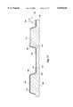
- FIG. 1is a side cross-sectional view of a mask coated substrate
- FIG. 2is a side cross-sectional view of the mask coated substrate of FIG. 1 having a portion of the coating removed to expose strips of the substrate;
- FIG. 3is an oblique view of the exposed substrate of FIG. 2;
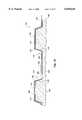
- FIG. 4is a side cross-sectional view of the mask coated substrate of FIG. 2 after etching of the substrate;
- FIG. 5is a side cross-sectional view of the etched substrate of FIG. 4 after removal of the mask strips;
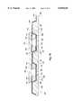
- FIG. 6is an oblique view of the etched substrate of FIG. 5;
- FIG. 7is a side cross-sectional view of the etched substrate of FIG. 5 coated with an insulating layer
- FIG. 8is a side cross-sectional view of the insulated substrate of FIG. 6 with a conductive coating
- FIG. 9is a side cross-sectional view of the insulated substrate of FIG. 6 with a multiple layer conductive coating
- FIG. 10is a side cross-sectional view of the conductively coated substrate of FIG. 8 after etching of the conductive coating to form conductive traces;
- FIG. 11is a side cross-sectional view of the conductive coated substrate of FIG. 8 after etching of the conductively coating to form conductive traces, bond wires being depicted to connect the conductive traces to external circuitry;
- FIG. 12is an oblique view of the conductively traced substrate of FIG. 11;
- FIG. 13is a side cross-sectional view of the conductive trace-bearing carrier substrate of FIG. 9 having select portions passivated;
- FIG. 14is a side cross-sectional view of the passivated carrier substrate of FIG. 13 with a semiconductor element flip-chip attached;
- FIG. 15is a side cross-sectional view of the passivated carrier substrate of FIG. 13 with a straddling semiconductor element flip-chip attached;
- FIG. 16is a side cross-sectional view of the passivated carrier substrate of FIG. 13 with an integrated circuitry-carrying, bond padded substrate attached;
- FIG. 17is a side cross-sectional view of the passivated carrier substrate of FIG. 13 in a stacked configuration with other such semiconductor-element carrying substrates;
- FIG. 18is a side cross-sectional view of a passivated, closely spaced mesa configuration with a straddling semiconductor element attached;
- FIG. 19is a side cross-sectional view of a wafer-to-wafer semiconductor element substrate arrangement
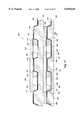
- FIG. 20is a top elevation of a box canyon mesa and conductive trace arrangement carrying a semiconductor element.
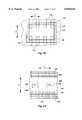
- FIG. 21is a top elevation of a carrier substrate bearing alignment boxes thereon for alignment of a semiconductor element therewith through engagement with alignment bumps or protrusions on the element.
- FIG. 1illustrates a mask coated carrier substrate 100.
- the mask coated substrate 100comprises a substrate 102 (such as monocrystalline silicon, silicon-on-glass, silicon-on-sapphire, germanium, or ceramic) coated with a mask layer 104, such as silicon nitride (Si 3 N 4 ).
- a substrate 102such as monocrystalline silicon, silicon-on-glass, silicon-on-sapphire, germanium, or ceramic
- a mask layer 104such as silicon nitride (Si 3 N 4 ).
- a semiconductor material substrateis currently preferred, other materials from which a substrate may be fabricated according to the present invention are equally suitable, subject to some limitations.
- a carrier substrate 102is preferably formed from a material having a coefficient of thermal expansion (CTE) that closely matches the CTE of the semiconductor die and/or other circuitry-bearing substrate (not shown) to be later attached to the completed carrier substrate.
- CTEcoefficient of thermal expansion
- the mask layer 104is etched to form mask layer strips 106, as shown in FIGS. 2 and 3.
- the substrate 102is then etched around the mask layer strips 106 to form elongated mesas 108 with sidewalls 110, as shown in FIG. 4.
- Typical etching techniquesinclude wet anisotropic etching with a solution of KOH:H 2 O. A 40% KOH solution applied at 70° C. can achieve etch rates of 30 ⁇ m/hr. This type of etching is also known in the art as bulk micro-machining. With such an anisotropic etch, the sidewalls 110 are formed with the elongated mesas 108 which are sloped at an angle of about 54° with the horizontal.
- the mask layer strips 106are removed, preferably using a wet etch.
- an etchantsuch as H 3 PO 4 , that is selective to the substrate, can be used.
- An insulating or dielectric layer 112is then formed on the substrate 102, including the elongated mesas 108 and the sidewalls 110, as shown in FIG. 7.
- the insulating layer 112is preferably formed by oxidating the substrate 102 and may be accomplished by exposing the substrate 102 to an oxidizing atmosphere in a reaction chamber.
- silicon dioxideis a preferred insulating layer 112 for its lower dielectric constant and consequently reduced capacitance, which results in increased speed of signal transmission in the overlying, subsequently-formed traces.
- a conductive material layer 114is then formed on the insulating layer 112.
- the conductive material layer 114can be any known, low resistivity material such as a metal, preferably palladium, tungsten, copper or aluminum. It can also be a stack of 2 or more metals, as noted below.
- the conductive material layer 114is preferably comprised of multiple layers. Most preferably, as shown in FIG. 9, the multiple layers are a chrome layer 118 applied over the insulating layer 112, a middle layer of copper/chrome alloy 120, followed by an uppermost layer of copper 122.
- This multiple layer configurationprovides both good adherence to the material of substrate 102 and an excellent wetting surface for the later attachment of the solder balls of semiconductor dice. Additionally, a fourth metal layer (not shown) of palladium or gold is occasionally placed atop the copper layer 122 to prevent oxidation of the copper. Furthermore, titanium or titanium/tungsten alloys may be used as alternatives to chrome, and nickel may be used as an alternative to copper.
- the conductive material layer 114is then masked, patterned and etched to form conductive traces 116, as shown in FIG. 10. It is also understood that the conductive traces 116 can be formed by a number of alternate conventional techniques, such as: depositing a conductive paste on the substrate by silk screening the conductive traces 116 directly thereon; directly extruding a conductive paste to form the conductive traces 116; or applying a second insulating layer on the insulating layer 112, etching a trough in the second insulating layer, filling the trough with a conductive material, and removing the excess conductive material.
- the conductive traces 116are preferably formed to include portions which extend over the mesas 108, up one sidewall 110, over the mesa top 111 and down the opposing mesa sidewall 110 onto the flat, etched portion 124 of the substrate 102 at chip mounting sites to form sidewall conductive trace terminal portions 126 and substrate conductive trace terminal portions 128, respectively.
- FIG. 10schematically illustrates an external connector 132, such as a lead, wire bonded or TAB tape attachment, in electrical communication with the conductive trace 116 abutting the substrate edge 130.
- the external connectors 132comprise bond wires 134, as shown in FIG. 11.
- FIG. 12illustrates an oblique view of the configuration shown in FIG. 11. It is understood that a different metal or uppermost metal layer (not shown) can be disposed on the conductive traces 116 near the substrate edge 130 to achieve a more effective site for bonding the external connector 132.
- the topmost metalcan be also optimized for direct electrical connection to electrical pins or other contacts, such as are used for spring-biased or plug-in connections to higher-level packaging.
- a passivation layer 136is optionally applied over the insulating layer 112 and conductive traces 116, and etched to expose contact areas 138 on the conductive traces 116, as shown in FIG. 13, to form a completed carrier substrate 140.
- the carrier substrate 140may be edge-connected into a mating aperture in a carrier of a higher-level package, the aperture including conductive clips arranged to connect to contact areas 138.
- the completed carrier substrate 140may accept numerous semiconductor dice and/or circuitry-carrying wafer or partial wafer (as noted previously, "semiconductor element") configurations.
- FIG. 14illustrates a conventional flip chip semiconductor element 142 attached to the carrier substrate 140.
- element 142is only one of a plurality of flip-chips 142 carried by substrate 140 in a multi-chip module (MCM) assembly such as a SIMM, DIMM, or mother board.
- MCMmulti-chip module
- a plurality of bond pads 144 on the flip chip 142achieves electrical contact with the conductive traces 116 via a plurality of conductive connectors 146, preferably lead/tin solder balls.
- the soldermay be sputtered, stenciled, screen-printed, evaporated or plated on bond pads 144, and then reflowed to produce a surface tension-constrained ball shape.
- solder ballsare reflowed at about 230° C.
- connections to the substratemay be enhanced by pre-placing a lead/tin solder paste at 117 on the exposed portions of conductive traces 116, which paste is formulated to reflow at a lower temperature than the solder balls.
- a lead/tin eutectic pastewhich will liquify at a temperature of about 160-180° C.
- solder ballsmay be sputtered, evaporated, screen-printed, stenciled or plated on terminal areas of conductive traces 116. By heating to this temperature after placing flip-chips 142 on substrate 140, both permanent and temporary electrical contact therebetween can be made.
- the lead/tin eutectic pastewhich liquifies at a lower temperature than the solder balls, may be employed to make a secure, temporary connection by heating the assembly to the lower temperature and then cooling to resolidify the paste, bonding the traces 116 to the solder balls. If a permanent connection is desired, a higher temperature may be employed to reflow the solder balls as well as the paste on the traces.
- the conductive connectors 146may be formed on either the flip chip 142 or the carrier substrate 140, as desired, the other element being configured with cooperative contacts. It is preferred, however, that conductive connectors be formed on flip chips 142.
- the conductive connectors 146each preferably make contact with both the sidewall conductive trace portion 126 and the substrate conductive trace portion 128.
- FIG. 15illustrates a straddling semiconductor chip or other circuitry-bearing semiconductor element 148 which spans one or more elongated mesas 108 and makes electrical contact with the conductive traces 116 in a manner discussed above for FIG. 14.
- mesas 108may be formed a single connector-width apart to provide the previously-referenced triple surface contact area.
- FIG. 16illustrates a semiconductor chip or integrated circuitry bearing element 150 with conductive connectors 152 designed to be angled to form a matched attachment to both the substrate conductive trace portion 128 and the sidewall conductive trace portion 126.
- the conductive connectors 152are preferably lead/tin connectors of square wedge or frustoconical configuration.
- These conductive connectors 152can be formed by sputtering or evaporating the conductive material, using conventional tin/lead solder compositions which liquify at about 230° C., or eutectic compositions which liquify at relatively low temperatures (about 160-180° C.), comprising about 63% by weight Pb and 37% by weight Sn, or by depositing the conductive material by stenciling, screen-printing, or plating the conductive material on top of conductive traces 116 on the carrier substrate 140 or on the bond pads 144 of the semiconductor chip 150.
- the lead/tin connectorsare formed by the above method, a single reflow during attachment of the semiconductor chip 150 to the carrier substrate 140 results in a simultaneous attachment and formation of a solder ball.
- a dielectric layer of relatively great thicknessmay be formed on the active surface of the die or carrier substrate to define the bond pad and solder ball locations to eliminate the need for an underfill.
- the connectorsmay be printed or otherwise formed of a conductive or conductor-filled epoxy with sidewalls angled to match those of the mesas.
- Such connectorsmay comprise a so-called "B stage" epoxy which is partially curable after deposition on the semiconductor element to stabilize its structure, and subsequently completely curable to effect an adhesive connection to the substrate traces.
- the conductive connectorsmay comprise conductive or conductor-filled thermoplastics. Non-conductive underfills between the substrate edge 130 and semiconductor chip 150 can also be employed to enhance the mechanical bond between the components and provide environmental protection in the electrical connections.
- the carrier substrate 140may be stacked with and attached to other semiconductor element-carrying substrates 140 with an adhesive 156, as shown in FIG. 17, to form a high density stacked configuration 158.
- FIG. 18illustrates a closely spaced, elongated mesa configuration with a straddling semiconductor 160 attached.
- the elongated mesas 108are spaced close enough together to make contact with three surfaces (i.e., a substrate etched portion 162, a first mesa sidewall surface 164, and a second mesa sidewall surface 166) of the conductive traces 116.
- three surfacesi.e., a substrate etched portion 162, a first mesa sidewall surface 164, and a second mesa sidewall surface 166
- FIG. 19illustrates a wafer-to-wafer arrangement 168.
- the wafer-to-wafer arrangement 168comprises a carrier substrate 170 formed from an entire silicon wafer attached, in a manner discussed above, to a semiconductor element 172 also formed from an entire wafer.
- FIG. 20illustrates the previously-noted "box canyon” arrangement of mesas 108 with conductive traces 116 extending thereover.
- solder ball connectors 146will result in automatic alignment of a semiconductor element 154 with the carrier substrate 140 in both X and Y directions upon solder reflow or, if conductive adhesive elements of precise placement, form and size are employed, during the assembly of the semiconductor element 154 with the carrier substrate 140, continued alignment being ensured by cure of the adhesive by heat, radiation, etc. as known in the art.
- FIG. 21illustrates the use of two alignment boxes 200 formed on a carrier substrate 140, which may be mated with like-spaced alignment bumps or protrusions 202 on a semiconductor element 154 to be attached to substrate 140, in order to effect precise X-Y alignment during initial placement of the semiconductor element 154.
- a single alignment box 200may be employed to ensure alignment in one of the X-Y directions, with mesas 108 flanking the alignment box or boxes 200 ensuring alignment in the other direction by their contact with solder ball connectors 146.
- Such alignment boxesare formed at the same time as the mesas, using the same substractive techniques. However, there are no traces formed on or over the alignment boxes.
- the alignment boxesmay also comprise C-shaped structures, or even two parallel “tabs” extending from the carrier substrate, if alignment in only one direction is required, or two alignment boxes comprising an "L” or chevron shape may be employed to cooperate with two spaced alignment bumps on the semiconductor element.
Landscapes
- Engineering & Computer Science (AREA)
- Computer Hardware Design (AREA)
- Microelectronics & Electronic Packaging (AREA)
- Power Engineering (AREA)
- Physics & Mathematics (AREA)
- Condensed Matter Physics & Semiconductors (AREA)
- General Physics & Mathematics (AREA)
- Wire Bonding (AREA)
- Micromachines (AREA)
Abstract
Description
Claims (35)
Priority Applications (4)
| Application Number | Priority Date | Filing Date | Title |
|---|---|---|---|
| US08/812,476US6040618A (en) | 1997-03-06 | 1997-03-06 | Multi-chip module employing a carrier substrate with micromachined alignment structures and method of forming |
| US09/008,678US6133065A (en) | 1997-03-06 | 1998-01-16 | Multi-chip module employing carrier substrate with micromachined alignment structures and method of forming |
| US09/652,880US6462399B1 (en) | 1997-03-06 | 2000-08-31 | Multi-chip module employing a carrier substrate with micromachined alignment structures and method of forming |
| US10/210,423US6664130B2 (en) | 1997-03-06 | 2002-07-31 | Methods of fabricating carrier substrates and semiconductor devices |
Applications Claiming Priority (1)
| Application Number | Priority Date | Filing Date | Title |
|---|---|---|---|
| US08/812,476US6040618A (en) | 1997-03-06 | 1997-03-06 | Multi-chip module employing a carrier substrate with micromachined alignment structures and method of forming |
Related Child Applications (1)
| Application Number | Title | Priority Date | Filing Date |
|---|---|---|---|
| US09/008,678DivisionUS6133065A (en) | 1997-03-06 | 1998-01-16 | Multi-chip module employing carrier substrate with micromachined alignment structures and method of forming |
Publications (1)
| Publication Number | Publication Date |
|---|---|
| US6040618Atrue US6040618A (en) | 2000-03-21 |
Family
ID=25209678
Family Applications (4)
| Application Number | Title | Priority Date | Filing Date |
|---|---|---|---|
| US08/812,476Expired - LifetimeUS6040618A (en) | 1997-03-06 | 1997-03-06 | Multi-chip module employing a carrier substrate with micromachined alignment structures and method of forming |
| US09/008,678Expired - LifetimeUS6133065A (en) | 1997-03-06 | 1998-01-16 | Multi-chip module employing carrier substrate with micromachined alignment structures and method of forming |
| US09/652,880Expired - LifetimeUS6462399B1 (en) | 1997-03-06 | 2000-08-31 | Multi-chip module employing a carrier substrate with micromachined alignment structures and method of forming |
| US10/210,423Expired - LifetimeUS6664130B2 (en) | 1997-03-06 | 2002-07-31 | Methods of fabricating carrier substrates and semiconductor devices |
Family Applications After (3)
| Application Number | Title | Priority Date | Filing Date |
|---|---|---|---|
| US09/008,678Expired - LifetimeUS6133065A (en) | 1997-03-06 | 1998-01-16 | Multi-chip module employing carrier substrate with micromachined alignment structures and method of forming |
| US09/652,880Expired - LifetimeUS6462399B1 (en) | 1997-03-06 | 2000-08-31 | Multi-chip module employing a carrier substrate with micromachined alignment structures and method of forming |
| US10/210,423Expired - LifetimeUS6664130B2 (en) | 1997-03-06 | 2002-07-31 | Methods of fabricating carrier substrates and semiconductor devices |
Country Status (1)
| Country | Link |
|---|---|
| US (4) | US6040618A (en) |
Cited By (25)
| Publication number | Priority date | Publication date | Assignee | Title |
|---|---|---|---|---|
| US6403493B2 (en) | 1999-11-19 | 2002-06-11 | Micron Technology, Inc. | Microelectronic device fabricating methods |
| US20020137303A1 (en)* | 2001-03-23 | 2002-09-26 | Micron Technology, Inc. | Reducing asymmetrically deposited film induced registration error |
| US6462399B1 (en)* | 1997-03-06 | 2002-10-08 | Micron Technology, Inc. | Multi-chip module employing a carrier substrate with micromachined alignment structures and method of forming |
| US20030067001A1 (en)* | 2001-10-08 | 2003-04-10 | Micron Technology, Inc. | Apparatus and method for packaging circuits |
| US20030094707A1 (en)* | 2001-08-30 | 2003-05-22 | Howarth James J. | Method of ball grid array (BGA) alignment, method of testing, alignment apparatus and semiconductor device assembly |
| US20030232488A1 (en)* | 2002-06-14 | 2003-12-18 | Chua Swee Kwang | Wafer level packaging |
| US6675469B1 (en)* | 1999-08-11 | 2004-01-13 | Tessera, Inc. | Vapor phase connection techniques |
| US6720664B1 (en)* | 2003-04-22 | 2004-04-13 | Tyntek Corporation | Submount-holder for flip chip package |
| US20040188811A1 (en)* | 2003-03-24 | 2004-09-30 | Intel Corporation | Circuit package apparatus, systems, and methods |
| US20040221451A1 (en)* | 2003-05-06 | 2004-11-11 | Micron Technology, Inc. | Method for packaging circuits and packaged circuits |
| US6836003B2 (en) | 1997-09-15 | 2004-12-28 | Micron Technology, Inc. | Integrated circuit package alignment feature |
| US6888256B2 (en)* | 2001-10-31 | 2005-05-03 | Infineon Technologies Ag | Compliant relief wafer level packaging |
| US20050184743A1 (en)* | 2004-02-24 | 2005-08-25 | Nihon Denshizairyo Kabushiki Kaisha | Probe card |
| US20060264064A1 (en)* | 2004-08-02 | 2006-11-23 | Micron Technology, Inc. | Zirconium-doped tantalum oxide films |
| US20070012938A1 (en)* | 2005-07-15 | 2007-01-18 | Chih-Kuang Yu | Light-emitting-diode packaging structure having thermal-electric element |
| US20070126445A1 (en)* | 2005-11-30 | 2007-06-07 | Micron Technology, Inc. | Integrated circuit package testing devices and methods of making and using same |
| US20090059609A1 (en)* | 2007-08-31 | 2009-03-05 | Marshall Joseph A | Starry sky lighting panels |
| US20100207266A1 (en)* | 2009-02-16 | 2010-08-19 | Industrial Technology Research Institute | Chip package structure |
| US20110309481A1 (en)* | 2010-06-18 | 2011-12-22 | Rui Huang | Integrated circuit packaging system with flip chip mounting and method of manufacture thereof |
| US20140361437A1 (en)* | 2013-06-11 | 2014-12-11 | SK Hynix Inc. | Package substrates and methods of fabricating the same |
| CN104894515A (en)* | 2015-05-27 | 2015-09-09 | 陕西斯瑞工业有限责任公司 | Electric-arc ion plating method for forming CuCr coating on surface of CuCr contact |
| US20190259721A1 (en)* | 2005-06-14 | 2019-08-22 | Cufer Asset Ltd. L.L.C. | Tooling for coupling multiple electronic chips |
| US10468400B2 (en) | 2017-02-03 | 2019-11-05 | Samsung Electronics Co., Ltd. | Method of manufacturing substrate structure |
| US11158219B2 (en)* | 2019-08-30 | 2021-10-26 | The Boeing Company | Exterior lighting in aircraft livery |
| WO2023187834A1 (en)* | 2022-03-30 | 2023-10-05 | Council Of Scientific And Industrial Research | Method for fabricating silicon chip carriers using wet bulk micromachining for ir detector applications |
Families Citing this family (38)
| Publication number | Priority date | Publication date | Assignee | Title |
|---|---|---|---|---|
| US6348739B1 (en)* | 1999-04-28 | 2002-02-19 | Matsushita Electric Industrial Co., Ltd. | Semiconductor device and method of manufacturing the same |
| US6344401B1 (en)* | 2000-03-09 | 2002-02-05 | Atmel Corporation | Method of forming a stacked-die integrated circuit chip package on a water level |
| DE60108413T2 (en) | 2000-11-10 | 2005-06-02 | Unitive Electronics, Inc. | METHOD FOR POSITIONING COMPONENTS WITH THE HELP OF LIQUID DRIVES AND STRUCTURES THEREFOR |
| US6580165B1 (en)* | 2000-11-16 | 2003-06-17 | Fairchild Semiconductor Corporation | Flip chip with solder pre-plated leadframe including locating holes |
| US6863209B2 (en) | 2000-12-15 | 2005-03-08 | Unitivie International Limited | Low temperature methods of bonding components |
| JP4048076B2 (en)* | 2001-07-10 | 2008-02-13 | 株式会社日本触媒 | Decomposition method of Michael adduct |
| US6744114B2 (en)* | 2001-08-29 | 2004-06-01 | Honeywell International Inc. | Package with integrated inductor and/or capacitor |
| US6762122B2 (en)* | 2001-09-27 | 2004-07-13 | Unitivie International Limited | Methods of forming metallurgy structures for wire and solder bonding |
| TWI292836B (en)* | 2001-10-31 | 2008-01-21 | Chi Mei Optoelectronics Corp | |
| US7579681B2 (en)* | 2002-06-11 | 2009-08-25 | Micron Technology, Inc. | Super high density module with integrated wafer level packages |
| WO2004001837A2 (en) | 2002-06-25 | 2003-12-31 | Unitive International Limited | Methods of forming electronic structures including conductive shunt layers and related structures |
| US7531898B2 (en) | 2002-06-25 | 2009-05-12 | Unitive International Limited | Non-Circular via holes for bumping pads and related structures |
| US7547623B2 (en) | 2002-06-25 | 2009-06-16 | Unitive International Limited | Methods of forming lead free solder bumps |
| KR100447851B1 (en)* | 2002-11-14 | 2004-09-08 | 삼성전자주식회사 | Wafer level Bonding method of flip-chip manner for semiconductor apparatus in lateral bonded type |
| TWI225899B (en) | 2003-02-18 | 2005-01-01 | Unitive Semiconductor Taiwan C | Etching solution and method for manufacturing conductive bump using the etching solution to selectively remove barrier layer |
| FI119583B (en) | 2003-02-26 | 2008-12-31 | Imbera Electronics Oy | Procedure for manufacturing an electronics module |
| TW577161B (en)* | 2003-04-17 | 2004-02-21 | Ftech Corp | Package structure having cavity |
| DE10320561B4 (en)* | 2003-05-07 | 2007-12-06 | Qimonda Ag | Method for producing a conductive connection between a semiconductor chip and an outer conductor structure |
| US7176106B2 (en)* | 2003-06-13 | 2007-02-13 | Avago Technologies Fiber Ip (Singapore) Pte. Ltd. | Wafer bonding using reactive foils for massively parallel micro-electromechanical systems packaging |
| TWI229928B (en)* | 2003-08-19 | 2005-03-21 | Advanced Semiconductor Eng | Semiconductor package structure |
| US7427557B2 (en)* | 2004-03-10 | 2008-09-23 | Unitive International Limited | Methods of forming bumps using barrier layers as etch masks |
| TW200603698A (en) | 2004-04-13 | 2006-01-16 | Unitive International Ltd | Methods of forming solder bumps on exposed metal pads and related structures |
| US8068346B2 (en) | 2004-05-04 | 2011-11-29 | Hamilton Sundstrand Corporation | Circuit board with high density power semiconductors |
| TWI239087B (en)* | 2004-07-23 | 2005-09-01 | Siliconware Precision Industries Co Ltd | Flip-chip semiconductor package with lead frame and method for fabricating the same |
| US7674701B2 (en) | 2006-02-08 | 2010-03-09 | Amkor Technology, Inc. | Methods of forming metal layers using multi-layer lift-off patterns |
| US7932615B2 (en) | 2006-02-08 | 2011-04-26 | Amkor Technology, Inc. | Electronic devices including solder bumps on compliant dielectric layers |
| US20080029686A1 (en)* | 2006-08-04 | 2008-02-07 | International Business Machines Corporation | Precision fabricated silicon mold |
| US7928582B2 (en)* | 2007-03-09 | 2011-04-19 | Micron Technology, Inc. | Microelectronic workpieces and methods for manufacturing microelectronic devices using such workpieces |
| KR100837281B1 (en)* | 2007-05-23 | 2008-06-11 | 삼성전자주식회사 | Semiconductor device package and manufacturing method thereof |
| US7999388B2 (en)* | 2007-09-24 | 2011-08-16 | Research Triangle Institute | Preventing breakage of long metal signal conductors on semiconductor substrates |
| US8158504B2 (en)* | 2008-05-30 | 2012-04-17 | E. I. Du Pont De Nemours And Company | Conductive compositions and processes for use in the manufacture of semiconductor devices—organic medium components |
| US20100084752A1 (en)* | 2008-10-08 | 2010-04-08 | Honeywell International Inc. | Systems and methods for implementing a wafer level hermetic interface chip |
| US20100320595A1 (en)* | 2009-06-22 | 2010-12-23 | Honeywell International Inc. | Hybrid hermetic interface chip |
| CN102339892A (en)* | 2010-07-20 | 2012-02-01 | 中晶(香港)有限公司 | Layer thin film device of ceramic substrate and production method |
| US8994048B2 (en) | 2010-12-09 | 2015-03-31 | Stats Chippac, Ltd. | Semiconductor device and method of forming recesses in substrate for same size or different sized die with vertical integration |
| JP2013129110A (en)* | 2011-12-21 | 2013-07-04 | Canon Inc | Substrate, liquid ejection head having the substrate and method of manufacturing the substrate |
| TWI644408B (en)* | 2016-12-05 | 2018-12-11 | 美商美光科技公司 | Interposer and semiconductor package |
| CN109920762B (en) | 2019-03-28 | 2021-12-03 | 京东方科技集团股份有限公司 | Manufacturing method of array substrate, array substrate and display device |
Citations (30)
| Publication number | Priority date | Publication date | Assignee | Title |
|---|---|---|---|---|
| US3379937A (en)* | 1962-04-27 | 1968-04-23 | Ferranti Ltd | Semiconductor circuit assemblies |
| US3508118A (en)* | 1965-12-13 | 1970-04-21 | Ibm | Circuit structure |
| US3974515A (en)* | 1974-09-12 | 1976-08-10 | Rca Corporation | IGFET on an insulating substrate |
| US4290079A (en)* | 1979-06-29 | 1981-09-15 | International Business Machines Corporation | Improved solder interconnection between a semiconductor device and a supporting substrate |
| US4376287A (en)* | 1980-10-29 | 1983-03-08 | Rca Corporation | Microwave power circuit with an active device mounted on a heat dissipating substrate |
| US4649627A (en)* | 1984-06-28 | 1987-03-17 | International Business Machines Corporation | Method of fabricating silicon-on-insulator transistors with a shared element |
| US4670770A (en)* | 1984-02-21 | 1987-06-02 | American Telephone And Telegraph Company | Integrated circuit chip-and-substrate assembly |
| US4680610A (en)* | 1983-11-30 | 1987-07-14 | Siemens Aktiengesellschaft | Semiconductor component comprising bump-like, metallic lead contacts and multilayer wiring |
| US4837609A (en)* | 1987-09-09 | 1989-06-06 | American Telephone And Telegraph Company, At&T Bell Laboratories | Semiconductor devices having superconducting interconnects |
| US4840302A (en)* | 1988-04-15 | 1989-06-20 | International Business Machines Corporation | Chromium-titanium alloy |
| US4948754A (en)* | 1987-09-02 | 1990-08-14 | Nippondenso Co., Ltd. | Method for making a semiconductor device |
| US5003357A (en)* | 1987-05-30 | 1991-03-26 | Samsung Semiconductor And Telecommunications Co. | Semiconductor light emitting device |
| US5006792A (en)* | 1989-03-30 | 1991-04-09 | Texas Instruments Incorporated | Flip-chip test socket adaptor and method |
| US5214308A (en)* | 1990-01-23 | 1993-05-25 | Sumitomo Electric Industries, Ltd. | Substrate for packaging a semiconductor device |
| US5326428A (en)* | 1993-09-03 | 1994-07-05 | Micron Semiconductor, Inc. | Method for testing semiconductor circuitry for operability and method of forming apparatus for testing semiconductor circuitry for operability |
| US5329423A (en)* | 1993-04-13 | 1994-07-12 | Scholz Kenneth D | Compressive bump-and-socket interconnection scheme for integrated circuits |
| US5352629A (en)* | 1993-01-19 | 1994-10-04 | General Electric Company | Process for self-alignment and planarization of semiconductor chips attached by solder die adhesive to multi-chip modules |
| US5376584A (en)* | 1992-12-31 | 1994-12-27 | International Business Machines Corporation | Process of making pad structure for solder ball limiting metallurgy having reduced edge stress |
| US5468995A (en)* | 1994-07-05 | 1995-11-21 | Motorola, Inc. | Semiconductor device having compliant columnar electrical connections |
| US5478779A (en)* | 1994-03-07 | 1995-12-26 | Micron Technology, Inc. | Electrically conductive projections and semiconductor processing method of forming same |
| US5483741A (en)* | 1993-09-03 | 1996-01-16 | Micron Technology, Inc. | Method for fabricating a self limiting silicon based interconnect for testing bare semiconductor dice |
| US5534465A (en)* | 1995-01-10 | 1996-07-09 | At&T Corp. | Method for making multichip circuits using active semiconductor substrates |
| US5559444A (en)* | 1991-06-04 | 1996-09-24 | Micron Technology, Inc. | Method and apparatus for testing unpackaged semiconductor dice |
| US5591941A (en)* | 1993-10-28 | 1997-01-07 | International Business Machines Corporation | Solder ball interconnected assembly |
| US5598036A (en)* | 1995-06-15 | 1997-01-28 | Industrial Technology Research Institute | Ball grid array having reduced mechanical stress |
| US5686317A (en)* | 1991-06-04 | 1997-11-11 | Micron Technology, Inc. | Method for forming an interconnect having a penetration limited contact structure for establishing a temporary electrical connection with a semiconductor die |
| US5712192A (en)* | 1994-04-26 | 1998-01-27 | International Business Machines Corporation | Process for connecting an electrical device to a circuit substrate |
| US5754408A (en)* | 1995-11-29 | 1998-05-19 | Mitsubishi Semiconductor America, Inc. | Stackable double-density integrated circuit assemblies |
| US5817540A (en)* | 1996-09-20 | 1998-10-06 | Micron Technology, Inc. | Method of fabricating flip-chip on leads devices and resulting assemblies |
| US5877556A (en)* | 1996-12-13 | 1999-03-02 | Industrial Technology Research Institute | Structure for composite bumps |
Family Cites Families (7)
| Publication number | Priority date | Publication date | Assignee | Title |
|---|---|---|---|---|
| US27934A (en)* | 1860-04-17 | Eyelet-machine | ||
| USRE27934E (en) | 1971-08-12 | 1974-03-05 | Circuit structure | |
| US3942245A (en)* | 1971-11-20 | 1976-03-09 | Ferranti Limited | Related to the manufacture of lead frames and the mounting of semiconductor devices thereon |
| US4480610A (en) | 1984-02-03 | 1984-11-06 | Joseph B. Stinson Co. | Remote oil level indicator |
| US4622574A (en)* | 1985-07-29 | 1986-11-11 | The Perkin-Elmer Corporation | Semiconductor chip with recessed bond pads |
| EP0971405A3 (en)* | 1994-09-23 | 2000-05-10 | Siemens S.A. | Method for manufacturing a substrate for a polymer stud grid array |
| US6040618A (en)* | 1997-03-06 | 2000-03-21 | Micron Technology, Inc. | Multi-chip module employing a carrier substrate with micromachined alignment structures and method of forming |
- 1997
- 1997-03-06USUS08/812,476patent/US6040618A/ennot_activeExpired - Lifetime
- 1998
- 1998-01-16USUS09/008,678patent/US6133065A/ennot_activeExpired - Lifetime
- 2000
- 2000-08-31USUS09/652,880patent/US6462399B1/ennot_activeExpired - Lifetime
- 2002
- 2002-07-31USUS10/210,423patent/US6664130B2/ennot_activeExpired - Lifetime
Patent Citations (30)
| Publication number | Priority date | Publication date | Assignee | Title |
|---|---|---|---|---|
| US3379937A (en)* | 1962-04-27 | 1968-04-23 | Ferranti Ltd | Semiconductor circuit assemblies |
| US3508118A (en)* | 1965-12-13 | 1970-04-21 | Ibm | Circuit structure |
| US3974515A (en)* | 1974-09-12 | 1976-08-10 | Rca Corporation | IGFET on an insulating substrate |
| US4290079A (en)* | 1979-06-29 | 1981-09-15 | International Business Machines Corporation | Improved solder interconnection between a semiconductor device and a supporting substrate |
| US4376287A (en)* | 1980-10-29 | 1983-03-08 | Rca Corporation | Microwave power circuit with an active device mounted on a heat dissipating substrate |
| US4680610A (en)* | 1983-11-30 | 1987-07-14 | Siemens Aktiengesellschaft | Semiconductor component comprising bump-like, metallic lead contacts and multilayer wiring |
| US4670770A (en)* | 1984-02-21 | 1987-06-02 | American Telephone And Telegraph Company | Integrated circuit chip-and-substrate assembly |
| US4649627A (en)* | 1984-06-28 | 1987-03-17 | International Business Machines Corporation | Method of fabricating silicon-on-insulator transistors with a shared element |
| US5003357A (en)* | 1987-05-30 | 1991-03-26 | Samsung Semiconductor And Telecommunications Co. | Semiconductor light emitting device |
| US4948754A (en)* | 1987-09-02 | 1990-08-14 | Nippondenso Co., Ltd. | Method for making a semiconductor device |
| US4837609A (en)* | 1987-09-09 | 1989-06-06 | American Telephone And Telegraph Company, At&T Bell Laboratories | Semiconductor devices having superconducting interconnects |
| US4840302A (en)* | 1988-04-15 | 1989-06-20 | International Business Machines Corporation | Chromium-titanium alloy |
| US5006792A (en)* | 1989-03-30 | 1991-04-09 | Texas Instruments Incorporated | Flip-chip test socket adaptor and method |
| US5214308A (en)* | 1990-01-23 | 1993-05-25 | Sumitomo Electric Industries, Ltd. | Substrate for packaging a semiconductor device |
| US5559444A (en)* | 1991-06-04 | 1996-09-24 | Micron Technology, Inc. | Method and apparatus for testing unpackaged semiconductor dice |
| US5686317A (en)* | 1991-06-04 | 1997-11-11 | Micron Technology, Inc. | Method for forming an interconnect having a penetration limited contact structure for establishing a temporary electrical connection with a semiconductor die |
| US5376584A (en)* | 1992-12-31 | 1994-12-27 | International Business Machines Corporation | Process of making pad structure for solder ball limiting metallurgy having reduced edge stress |
| US5352629A (en)* | 1993-01-19 | 1994-10-04 | General Electric Company | Process for self-alignment and planarization of semiconductor chips attached by solder die adhesive to multi-chip modules |
| US5329423A (en)* | 1993-04-13 | 1994-07-12 | Scholz Kenneth D | Compressive bump-and-socket interconnection scheme for integrated circuits |
| US5326428A (en)* | 1993-09-03 | 1994-07-05 | Micron Semiconductor, Inc. | Method for testing semiconductor circuitry for operability and method of forming apparatus for testing semiconductor circuitry for operability |
| US5483741A (en)* | 1993-09-03 | 1996-01-16 | Micron Technology, Inc. | Method for fabricating a self limiting silicon based interconnect for testing bare semiconductor dice |
| US5591941A (en)* | 1993-10-28 | 1997-01-07 | International Business Machines Corporation | Solder ball interconnected assembly |
| US5478779A (en)* | 1994-03-07 | 1995-12-26 | Micron Technology, Inc. | Electrically conductive projections and semiconductor processing method of forming same |
| US5712192A (en)* | 1994-04-26 | 1998-01-27 | International Business Machines Corporation | Process for connecting an electrical device to a circuit substrate |
| US5468995A (en)* | 1994-07-05 | 1995-11-21 | Motorola, Inc. | Semiconductor device having compliant columnar electrical connections |
| US5534465A (en)* | 1995-01-10 | 1996-07-09 | At&T Corp. | Method for making multichip circuits using active semiconductor substrates |
| US5598036A (en)* | 1995-06-15 | 1997-01-28 | Industrial Technology Research Institute | Ball grid array having reduced mechanical stress |
| US5754408A (en)* | 1995-11-29 | 1998-05-19 | Mitsubishi Semiconductor America, Inc. | Stackable double-density integrated circuit assemblies |
| US5817540A (en)* | 1996-09-20 | 1998-10-06 | Micron Technology, Inc. | Method of fabricating flip-chip on leads devices and resulting assemblies |
| US5877556A (en)* | 1996-12-13 | 1999-03-02 | Industrial Technology Research Institute | Structure for composite bumps |
Cited By (62)
| Publication number | Priority date | Publication date | Assignee | Title |
|---|---|---|---|---|
| US6664130B2 (en) | 1997-03-06 | 2003-12-16 | Micron Technology, Inc. | Methods of fabricating carrier substrates and semiconductor devices |
| US6462399B1 (en)* | 1997-03-06 | 2002-10-08 | Micron Technology, Inc. | Multi-chip module employing a carrier substrate with micromachined alignment structures and method of forming |
| US6836003B2 (en) | 1997-09-15 | 2004-12-28 | Micron Technology, Inc. | Integrated circuit package alignment feature |
| US6858453B1 (en) | 1997-09-15 | 2005-02-22 | Micron Technology, Inc. | Integrated circuit package alignment feature |
| US20040075991A1 (en)* | 1999-08-11 | 2004-04-22 | Tessera. Inc. | Vapor phase connection techniques |
| US6675469B1 (en)* | 1999-08-11 | 2004-01-13 | Tessera, Inc. | Vapor phase connection techniques |
| US6873050B2 (en)* | 1999-11-19 | 2005-03-29 | Micron Technology, Inc. | Intermediate construction having an edge defined feature |
| US20050202674A1 (en)* | 1999-11-19 | 2005-09-15 | Reinberg Alan R. | Microelectronic device fabricating method, integrated circuit, and intermediate construction |
| US20020163061A1 (en)* | 1999-11-19 | 2002-11-07 | Reinberg Alan R. | Microelectronic device fabricating method, integrated circuit, and intermediate construction |
| US6897540B1 (en)* | 1999-11-19 | 2005-05-24 | Micron Technology, Inc. | Microelectronic device fabricating method, integrated circuit, and intermediate construction |
| US6403493B2 (en) | 1999-11-19 | 2002-06-11 | Micron Technology, Inc. | Microelectronic device fabricating methods |
| US6429125B2 (en) | 1999-11-19 | 2002-08-06 | Micron Technology, Inc. | Microelectronic device fabricating method |
| US7127319B2 (en) | 2001-03-23 | 2006-10-24 | Micron Technology, Inc. | Reducing asymmetrically deposited film induced registration error |
| US6486956B2 (en) | 2001-03-23 | 2002-11-26 | Micron Technology, Inc. | Reducing asymmetrically deposited film induced registration error |
| US6852456B2 (en) | 2001-03-23 | 2005-02-08 | Micron Technology, Inc. | Reducing asymmetrically deposited film induced registration error |
| US6795747B2 (en) | 2001-03-23 | 2004-09-21 | Micron Technology, Inc. | Reducing asymmetrically deposited film induced registration error |
| US20020137303A1 (en)* | 2001-03-23 | 2002-09-26 | Micron Technology, Inc. | Reducing asymmetrically deposited film induced registration error |
| US20050027388A1 (en)* | 2001-03-23 | 2005-02-03 | Micron Technology, Inc. | Reducing asymmetrically deposited film induced registration error |
| US6963143B2 (en) | 2001-08-30 | 2005-11-08 | Micron Technology, Inc. | Method of ball grid array (BGA) alignment, method of testing, alignment apparatus and semiconductor device assembly |
| US20030094707A1 (en)* | 2001-08-30 | 2003-05-22 | Howarth James J. | Method of ball grid array (BGA) alignment, method of testing, alignment apparatus and semiconductor device assembly |
| US7005754B2 (en) | 2001-08-30 | 2006-02-28 | Micron Technology, Inc. | Method of ball grid array (BGA) alignment, method of testing, alignment apparatus and semiconductor device assembly |
| US6991960B2 (en) | 2001-08-30 | 2006-01-31 | Micron Technology, Inc. | Method of semiconductor device package alignment and method of testing |
| US7675169B2 (en) | 2001-10-08 | 2010-03-09 | Micron Technology, Inc. | Apparatus and method for packaging circuits |
| US20100140794A1 (en)* | 2001-10-08 | 2010-06-10 | Chia Yong Poo | Apparatus and method for packaging circuits |
| US7358154B2 (en) | 2001-10-08 | 2008-04-15 | Micron Technology, Inc. | Method for fabricating packaged die |
| US8115306B2 (en) | 2001-10-08 | 2012-02-14 | Round Rock Research, Llc | Apparatus and method for packaging circuits |
| US6894386B2 (en) | 2001-10-08 | 2005-05-17 | Micron Technology, Inc. | Apparatus and method for packaging circuits |
| US20050029668A1 (en)* | 2001-10-08 | 2005-02-10 | Micron Technology, Inc. | Apparatus and method for packaging circuits |
| US20080054423A1 (en)* | 2001-10-08 | 2008-03-06 | Micron Technology, Inc. | Apparatus and method for packaging circuits |
| US8138617B2 (en) | 2001-10-08 | 2012-03-20 | Round Rock Research, Llc | Apparatus and method for packaging circuits |
| US20060084240A1 (en)* | 2001-10-08 | 2006-04-20 | Micron Technology, Inc. | Apparatus and method for packaging circuits |
| US20030067001A1 (en)* | 2001-10-08 | 2003-04-10 | Micron Technology, Inc. | Apparatus and method for packaging circuits |
| US6888256B2 (en)* | 2001-10-31 | 2005-05-03 | Infineon Technologies Ag | Compliant relief wafer level packaging |
| US20110018143A1 (en)* | 2002-06-14 | 2011-01-27 | Swee Kwang Chua | Wafer level packaging |
| US8106488B2 (en) | 2002-06-14 | 2012-01-31 | Micron Technology, Inc. | Wafer level packaging |
| US8564106B2 (en) | 2002-06-14 | 2013-10-22 | Micron Technology, Inc. | Wafer level packaging |
| US20030232488A1 (en)* | 2002-06-14 | 2003-12-18 | Chua Swee Kwang | Wafer level packaging |
| US7375009B2 (en) | 2002-06-14 | 2008-05-20 | Micron Technology, Inc. | Method of forming a conductive via through a wafer |
| US20040188811A1 (en)* | 2003-03-24 | 2004-09-30 | Intel Corporation | Circuit package apparatus, systems, and methods |
| US6720664B1 (en)* | 2003-04-22 | 2004-04-13 | Tyntek Corporation | Submount-holder for flip chip package |
| US8555495B2 (en) | 2003-05-06 | 2013-10-15 | Micron Technology, Inc. | Method for packaging circuits |
| US7712211B2 (en) | 2003-05-06 | 2010-05-11 | Micron Technology, Inc. | Method for packaging circuits and packaged circuits |
| US10811278B2 (en) | 2003-05-06 | 2020-10-20 | Micron Technology, Inc. | Method for packaging circuits |
| US20100146780A1 (en)* | 2003-05-06 | 2010-06-17 | Yong Poo Chia | Method for packaging circuits and packaged circuits |
| US10453704B2 (en) | 2003-05-06 | 2019-10-22 | Micron Technology, Inc. | Method for packaging circuits |
| US9484225B2 (en) | 2003-05-06 | 2016-11-01 | Micron Technology, Inc. | Method for packaging circuits |
| US8065792B2 (en) | 2003-05-06 | 2011-11-29 | Micron Technology, Inc. | Method for packaging circuits |
| US20040221451A1 (en)* | 2003-05-06 | 2004-11-11 | Micron Technology, Inc. | Method for packaging circuits and packaged circuits |
| US20050184743A1 (en)* | 2004-02-24 | 2005-08-25 | Nihon Denshizairyo Kabushiki Kaisha | Probe card |
| US20060264064A1 (en)* | 2004-08-02 | 2006-11-23 | Micron Technology, Inc. | Zirconium-doped tantalum oxide films |
| US20190259721A1 (en)* | 2005-06-14 | 2019-08-22 | Cufer Asset Ltd. L.L.C. | Tooling for coupling multiple electronic chips |
| US20070012938A1 (en)* | 2005-07-15 | 2007-01-18 | Chih-Kuang Yu | Light-emitting-diode packaging structure having thermal-electric element |
| US20070126445A1 (en)* | 2005-11-30 | 2007-06-07 | Micron Technology, Inc. | Integrated circuit package testing devices and methods of making and using same |
| US8033684B2 (en)* | 2007-08-31 | 2011-10-11 | The Boeing Company | Starry sky lighting panels |
| US20090059609A1 (en)* | 2007-08-31 | 2009-03-05 | Marshall Joseph A | Starry sky lighting panels |
| US20100207266A1 (en)* | 2009-02-16 | 2010-08-19 | Industrial Technology Research Institute | Chip package structure |
| US20110309481A1 (en)* | 2010-06-18 | 2011-12-22 | Rui Huang | Integrated circuit packaging system with flip chip mounting and method of manufacture thereof |
| US20140361437A1 (en)* | 2013-06-11 | 2014-12-11 | SK Hynix Inc. | Package substrates and methods of fabricating the same |
| CN104894515A (en)* | 2015-05-27 | 2015-09-09 | 陕西斯瑞工业有限责任公司 | Electric-arc ion plating method for forming CuCr coating on surface of CuCr contact |
| US10468400B2 (en) | 2017-02-03 | 2019-11-05 | Samsung Electronics Co., Ltd. | Method of manufacturing substrate structure |
| US11158219B2 (en)* | 2019-08-30 | 2021-10-26 | The Boeing Company | Exterior lighting in aircraft livery |
| WO2023187834A1 (en)* | 2022-03-30 | 2023-10-05 | Council Of Scientific And Industrial Research | Method for fabricating silicon chip carriers using wet bulk micromachining for ir detector applications |
Also Published As
| Publication number | Publication date |
|---|---|
| US6133065A (en) | 2000-10-17 |
| US20020185704A1 (en) | 2002-12-12 |
| US6664130B2 (en) | 2003-12-16 |
| US6462399B1 (en) | 2002-10-08 |
Similar Documents
| Publication | Publication Date | Title |
|---|---|---|
| US6040618A (en) | Multi-chip module employing a carrier substrate with micromachined alignment structures and method of forming | |
| US9613922B2 (en) | Semiconductor device and manufacturing method thereof | |
| US6229711B1 (en) | Flip-chip mount board and flip-chip mount structure with improved mounting reliability | |
| US6407451B2 (en) | Micromachined chip scale package | |
| US6259608B1 (en) | Conductor pattern for surface mount devices and method therefor | |
| US8174105B2 (en) | Stacked semiconductor package having discrete components | |
| US8097947B2 (en) | Conductive systems and devices including wires coupled to anisotropic conductive film, and methods of forming the same | |
| US7218005B2 (en) | Compact semiconductor device capable of mounting a plurality of semiconductor chips with high density and method of manufacturing the same | |
| US5942795A (en) | Leaded substrate carrier for integrated circuit device and leaded substrate carrier device assembly | |
| US20050167850A1 (en) | Flip-chip adaptor package for bare die | |
| KR20150041029A (en) | BVA interposer | |
| US7074704B2 (en) | Bump formed on semiconductor device chip and method for manufacturing the bump | |
| JP2011142185A (en) | Semiconductor device | |
| US5569956A (en) | Interposer connecting leadframe and integrated circuit | |
| JPH0239097B2 (en) | ||
| KR100469543B1 (en) | Standardized bonding location process and apparatus | |
| US6306748B1 (en) | Bump scrub after plating | |
| US6433415B2 (en) | Assembly of plurality of semiconductor devices | |
| JPH03192742A (en) | Connection of electric circuit component | |
| JPH039620B2 (en) | ||
| JPS62199023A (en) | Mounting method for semiconductor devices | |
| JP2000133750A (en) | Semiconductor device | |
| JPH0922956A (en) | Semiconductor device |
Legal Events
| Date | Code | Title | Description |
|---|---|---|---|
| AS | Assignment | Owner name:MICRON TECHNOLOGY, INC., IDAHO Free format text:ASSIGNMENT OF ASSIGNORS INTEREST;ASSIGNOR:AKRAM, SALMAN;REEL/FRAME:008421/0765 Effective date:19970305 | |
| STCF | Information on status: patent grant | Free format text:PATENTED CASE | |
| CC | Certificate of correction | ||
| FPAY | Fee payment | Year of fee payment:4 | |
| FEPP | Fee payment procedure | Free format text:PAYOR NUMBER ASSIGNED (ORIGINAL EVENT CODE: ASPN); ENTITY STATUS OF PATENT OWNER: LARGE ENTITY | |
| FPAY | Fee payment | Year of fee payment:8 | |
| FPAY | Fee payment | Year of fee payment:12 | |
| AS | Assignment | Owner name:U.S. BANK NATIONAL ASSOCIATION, AS COLLATERAL AGENT, CALIFORNIA Free format text:SECURITY INTEREST;ASSIGNOR:MICRON TECHNOLOGY, INC.;REEL/FRAME:038669/0001 Effective date:20160426 Owner name:U.S. BANK NATIONAL ASSOCIATION, AS COLLATERAL AGEN Free format text:SECURITY INTEREST;ASSIGNOR:MICRON TECHNOLOGY, INC.;REEL/FRAME:038669/0001 Effective date:20160426 | |
| AS | Assignment | Owner name:MORGAN STANLEY SENIOR FUNDING, INC., AS COLLATERAL AGENT, MARYLAND Free format text:PATENT SECURITY AGREEMENT;ASSIGNOR:MICRON TECHNOLOGY, INC.;REEL/FRAME:038954/0001 Effective date:20160426 Owner name:MORGAN STANLEY SENIOR FUNDING, INC., AS COLLATERAL Free format text:PATENT SECURITY AGREEMENT;ASSIGNOR:MICRON TECHNOLOGY, INC.;REEL/FRAME:038954/0001 Effective date:20160426 | |
| AS | Assignment | Owner name:U.S. BANK NATIONAL ASSOCIATION, AS COLLATERAL AGENT, CALIFORNIA Free format text:CORRECTIVE ASSIGNMENT TO CORRECT THE REPLACE ERRONEOUSLY FILED PATENT #7358718 WITH THE CORRECT PATENT #7358178 PREVIOUSLY RECORDED ON REEL 038669 FRAME 0001. ASSIGNOR(S) HEREBY CONFIRMS THE SECURITY INTEREST;ASSIGNOR:MICRON TECHNOLOGY, INC.;REEL/FRAME:043079/0001 Effective date:20160426 Owner name:U.S. BANK NATIONAL ASSOCIATION, AS COLLATERAL AGEN Free format text:CORRECTIVE ASSIGNMENT TO CORRECT THE REPLACE ERRONEOUSLY FILED PATENT #7358718 WITH THE CORRECT PATENT #7358178 PREVIOUSLY RECORDED ON REEL 038669 FRAME 0001. ASSIGNOR(S) HEREBY CONFIRMS THE SECURITY INTEREST;ASSIGNOR:MICRON TECHNOLOGY, INC.;REEL/FRAME:043079/0001 Effective date:20160426 | |
| AS | Assignment | Owner name:MICRON TECHNOLOGY, INC., IDAHO Free format text:RELEASE BY SECURED PARTY;ASSIGNOR:U.S. BANK NATIONAL ASSOCIATION, AS COLLATERAL AGENT;REEL/FRAME:047243/0001 Effective date:20180629 | |
| AS | Assignment | Owner name:MICRON TECHNOLOGY, INC., IDAHO Free format text:RELEASE BY SECURED PARTY;ASSIGNOR:MORGAN STANLEY SENIOR FUNDING, INC., AS COLLATERAL AGENT;REEL/FRAME:050937/0001 Effective date:20190731 |