US6040544A - Optoelectronic separation apparatus - Google Patents
Optoelectronic separation apparatusDownload PDFInfo
- Publication number
- US6040544A US6040544AUS09/075,033US7503398AUS6040544AUS 6040544 AUS6040544 AUS 6040544AUS 7503398 AUS7503398 AUS 7503398AUS 6040544 AUS6040544 AUS 6040544A
- Authority
- US
- United States
- Prior art keywords
- semiconductor material
- separated
- slide face
- separating
- separation
- Prior art date
- Legal status (The legal status is an assumption and is not a legal conclusion. Google has not performed a legal analysis and makes no representation as to the accuracy of the status listed.)
- Expired - Lifetime
Links
Images


Classifications
- B—PERFORMING OPERATIONS; TRANSPORTING
- B07—SEPARATING SOLIDS FROM SOLIDS; SORTING
- B07C—POSTAL SORTING; SORTING INDIVIDUAL ARTICLES, OR BULK MATERIAL FIT TO BE SORTED PIECE-MEAL, e.g. BY PICKING
- B07C5/00—Sorting according to a characteristic or feature of the articles or material being sorted, e.g. by control effected by devices which detect or measure such characteristic or feature; Sorting by manually actuated devices, e.g. switches
- B07C5/36—Sorting apparatus characterised by the means used for distribution
- B07C5/363—Sorting apparatus characterised by the means used for distribution by means of air
- B07C5/367—Sorting apparatus characterised by the means used for distribution by means of air using a plurality of separation means
- B07C5/368—Sorting apparatus characterised by the means used for distribution by means of air using a plurality of separation means actuated independently
- B—PERFORMING OPERATIONS; TRANSPORTING
- B07—SEPARATING SOLIDS FROM SOLIDS; SORTING
- B07C—POSTAL SORTING; SORTING INDIVIDUAL ARTICLES, OR BULK MATERIAL FIT TO BE SORTED PIECE-MEAL, e.g. BY PICKING
- B07C5/00—Sorting according to a characteristic or feature of the articles or material being sorted, e.g. by control effected by devices which detect or measure such characteristic or feature; Sorting by manually actuated devices, e.g. switches
- B07C5/04—Sorting according to size
- B07C5/10—Sorting according to size measured by light-responsive means
- B—PERFORMING OPERATIONS; TRANSPORTING
- B07—SEPARATING SOLIDS FROM SOLIDS; SORTING
- B07C—POSTAL SORTING; SORTING INDIVIDUAL ARTICLES, OR BULK MATERIAL FIT TO BE SORTED PIECE-MEAL, e.g. BY PICKING
- B07C5/00—Sorting according to a characteristic or feature of the articles or material being sorted, e.g. by control effected by devices which detect or measure such characteristic or feature; Sorting by manually actuated devices, e.g. switches
- B07C5/36—Sorting apparatus characterised by the means used for distribution
- B07C5/363—Sorting apparatus characterised by the means used for distribution by means of air
- B07C5/367—Sorting apparatus characterised by the means used for distribution by means of air using a plurality of separation means
Definitions
- the present inventionrelates to an apparatus and a method for the optoelectronic classification and separation of semiconductor material.
- High-purity semiconductor materialis required for the production of solar cells or electronic components, such as for example storage elements or microprocessors.
- the dopants introduced in a targeted mannerare the only impurities which, in the most favorable case, a material of this kind should contain. It is therefore desirable to keep the concentration of harmful impurities as low as possible. It is frequently observed that even semiconductor material which has been produced to a high level of purity is recontaminated during further processing to give the desired products. For this reason, complex cleaning steps are required again and again in order to regain the original level of purity. Atoms of foreign metals which become incorporated into the crystal lattice of the semiconductor material can interfere with the charge distribution. These atoms can reduce the performance of the ultimate component or lead to its failure.
- siliconwhich is the most frequently used semiconductor material in the electronics industry.
- High-purity siliconis obtained, for example, by the thermal decomposition of silicon compounds which are highly volatile, and are therefore easy to purify using a distillation method, such as for example trichlorosilane.
- the siliconis obtained in the form of polycrystalline rods with typical diameters of from 70 to 300 mm and lengths of from 500 to 2500 mm. A large proportion of the rods are used to produce crucible-pulled monocrystals, strips or sheets, or to produce polycrystalline solar-cell base material.
- the semiconductor materialis present in various fragment sizes.
- numerous semiconductor materialssuch as primarily polysilicon, have to be present in a specific fragment size distribution for the melting operation. Since it is not permissible for any impurities to pass into the crucible together with the semiconductor material, very particular demands have to be placed on both the crushing process and on the classification process, so that there is no contamination from atoms of foreign material emanating from metallic tools, such as for example screening apparatus. This fact precludes conventional screening apparatus which are commercially available.
- an apparatus and a methodare provided for the separation and classification of semiconductor material, in particular of silicon, in which the semiconductor material is contaminated with metal atoms to the lowest possible degree.
- a suitably accurate cut-off pointcan be set, and as little abrasion as possible will result. Also there are no holes which can become blocked.
- the present inventionachieves these unexpected results which are surprisingly unique in view of the prior art.
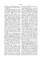
- FIGUREshows an apparatus according to the invention.
- FIGUREshows an apparatus for the optoelectronic classification and separation of semiconductor materials, wherein the apparatus has a separating device 2 and a slide face 3.
- the angle of the slide face 3is adjustable to the horizontal.
- the separating device 2 and the slide face 3each have a surface made of the semiconductor material to be classified, and a radiation source 5, through the beam path 4 of which the material to be classified falls.
- a shape recognition device 6transmits the shape of the material to be classified to a control unit 7, which controls at least one diverter device 8.
- the apparatusis preferably used to classify hard, brittle semiconductor materials, such as silicon, germanium or gallium arsenide according to grain size. It is preferably used to classify and separate silicon. This apparatus can also be used to separate semiconductor material into two or more grain-size fractions.
- the apparatusis designed in such a way that the material 1 to be classified and separated firstly passes onto a device for separating and preferably for simultaneously conveying, which is preferably a vibrating conveyor.
- This vibrating conveyoris preferably subjected to vibrations which separate the fragments of semiconductor material and convey them in the direction of the slide face 3.
- the angle of this slide face 3is adjustable with respect to the horizontal; it is set as a function of the coefficient of friction between fragment and surface covering in such a manner that the fragments preferably slide downward under the action of the force of gravity.
- the angleis set within a range from 20° to 80°, preferably 30° to 70°.
- This device 2 for separating and preferably for conveying, and the slide face 3are designed in such a way that the semiconductor material to be classified does not come into contact, on their surfaces, with materials other than the semiconductor material to be classified. This is preferably carried out by coating this device 2 for separating and preferably for conveying and the slide face 3 with the same semiconductor material as that which is to be classified.
- the separating device 2 and the slide face 3may also be made entirely from the appropriate semiconductor material. Therefore, in the case of silicon, this means that they may be coated with silicon or consist of silicon.
- the pieces of materialalign themselves in such a manner that their center of gravity comes to lie at as low a level as possible. This means that during their free fall after passing over the slide face 3, their largest projection surface faces the radiation source 5.
- the height of the fall between the slide face 3 and the diverter device 8is preferably 5 cm to 20 cm, particularly 10 cm.
- a radiation source 5 and a shape recognition device 6are arranged approximately in the center of this falling distance, the piece of material moving between the radiation source 5 and the shape recognition device 6.
- the distance between the piece of material and the radiation source 5is preferably 50 cm to 120 cm, particularly preferably 70 cm.
- the distance between the piece of material and the shape recognition device 6is preferably 5 cm to 12 cm, particularly preferably 6 cm.
- the radiation source 5is preferably an electromagnetic radiation source, such as a laser, or a lamp which emits visible light in the range from 400 nm to 700 nm. It is also possible to emit electromagnetic radiation in the infrared range, in the ultraviolet range or in the X-ray range.
- the shape recognition device 6is preferably a high-resolution sensor, which may be a camera, for detecting visible light, infrared rays, ultraviolet rays or X-rays.
- This sensoris connected to a control unit 7, which evaluates the data received.
- This control unit 7is preferably a computer.
- This control unit 7controls at least one diverter device 8 using a predetermined program.
- this recognition systemcomprising control unit 7 and shape recognition device 6, can detect a specific grain size or a grain-size range.
- the diverter device 8, which captures the appropriate grain size or a grain-size range,is preferably a nozzle from which, preferably, gases or liquids can be ejected.
- the gasespreferably are air or inert gases, such as nitrogen, which can be ejected at a pressure of above atmospheric pressure, preferably at 3 to 10 bar, particularly preferably at 6 bar.
- the liquidspreferably high-purity water, having a conductance of preferably below 0.14 uS, particularly preferably of 0.08 uS, is ejected at a pressure of preferably 2 to 20 bar.
- a piece of material which is too largeis subjected to comminution using a water jet at preferably 1500 bar to 5000 bar, particularly preferably at 3500 bar.
- the diverter device 8may be arranged on its own or may comprise a plurality of nozzles which are arranged next to one another. These nozzles are preferably arranged in a series at intervals of preferably 3 to 15 mm, particularly preferably of 9 mm, when the pieces of material fall in parallel through the beam path 4 of the radiation source 5.
- the diverted pieces of material of the desired grain size or grain-size rangeare preferably collected in a collection container 10 via a separating device 9.
- the pieces of material which have not been divertedare collected in a collection container 11.
- the collection containersmay have a surface made of the semiconductor material to be classified, or the containers may consist of this material.
- the two separated streams of materialcan be divided into further grain classes by means of further recognition systems and diverter devices. It is likewise possible to carry out classification in accordance with surface parameters.
- the provision of further separating devices 9would also enable material to be separated into a plurality of grain classes. In this case the falling path is divided up by diversion effects of different strengths, preferably by air blasts of different strengths.
- This separating device 9is preferably provided on the surface with the semiconductor material to be classified, or consists of this material.
- the present inventionis also directed to a method for the optoelectronic classification and separation of semiconductor materials by means of the apparatus according to the invention for optoelectronic classification and separation.
- the material to be classifiedis separated on a separating device 2, which has the semiconductor material to be classified on its surface, and slides downward over a slide face 3.
- Slide face 3has the semiconductor material to be classified on its surface.
- the angle of the slide faceis adjustable to the horizontal by an adjustment means, so that the center of gravity of the material to be classified and separated lies as low as possible.
- This material, after leaving the slide face 3 in this alignmentpasses through the beam path of a radiation source 5.
- a shape recognition device 6transmits the shape of the material to be classified to a control unit 7.
- This control unitin accordance with preset criteria controls at least one diverter device 8 which diverts the material to be classified.
- the comminuted material 1, in this case semiconductor materialis conveyed in a separating device 2 toward a slide face 3.
- the angle of the slide face 3is adjusted, as a function of the coefficient of friction between the semiconductor material to be classified and separated and the surface coating. This adjustment is made in such a manner that the semiconductor material to be separated slides downward, preferably under the force of gravity.
- the irregularly shaped semiconductor materialaligns itself in such a manner that its center of gravity comes to lie at as low a level as possible.
- the materialhas its largest projection surface facing toward the slide face 3. Aligned in this way, the comminuted material, after leaving the slide face 3, moves past the recognition system, which comprises radiation source 5 and shape recognition device 6.
- the materialmoves past the beam path 4 of the radiation source 5, and is detected by a shape recognition device 6.
- Device 6preferably has an optical resolution of 0.1 mm to 20 mm, and particularly preferably has an optical resolution of 0.5 mm to 10 mm, the data obtained being evaluated by a control unit 7.
- the semiconductor material to be classifiedmoves past the recognition system over a falling period of 0.05 sec to 1 sec, particularly preferably from 0.1 sec to 0.2 sec.
- at least one diverter device 8is activated. This device 8 diverts, for example, all the semiconductor material pieces which are too small using, for example, an air jet, thus deflecting them out of their original falling path.
- a separating device 9separates the two fractions, which are collected in separate collection containers 10 and 11.
- the method according to the inventionin combination with the apparatus according to the invention, has the advantages that classification and separation is carried out without contamination.
- a range of from 15 mm to 150 mmis classified and separated in a continuously variable manner.
- itcan also be set in such a way that a range of, for example, 10 to 20 mm is captured or a specific percentage of a certain grain size is captured, mixed with a percentage of another specific grain size.
- adjustable loading chargesprecisely as desired by the purchasers, who need specific grain-size distributions in order to fill the crucible from which, for example, the monocrystal is to be pulled.
- Exampledisclose an embodiment of the present invention. It should be understood, however, that the Example is designed for the purpose of illustration only and not as a definition of the limits of the invention.
- a preferred embodiment of the apparatus according to the invention for optoelectronic classification and separationhas an operating width of, for example, 500 mm, an optical resolution of 0.5 mm and a nozzle array arranged at a spacing of 8 mm, classifying a volumetric flow of 1 t/h from a pile of polysilicon fragments of different sizes with a grain separation size of 30 mm and a sharp cut-off point.
Landscapes
- Combined Means For Separation Of Solids (AREA)
- Sorting Of Articles (AREA)
- Silicon Compounds (AREA)
- Length Measuring Devices By Optical Means (AREA)
Abstract
Description
Claims (7)
Applications Claiming Priority (2)
| Application Number | Priority Date | Filing Date | Title |
|---|---|---|---|
| DE19719698ADE19719698A1 (en) | 1997-05-09 | 1997-05-09 | Optoelectronic classifying device |
| DE19719698 | 1997-05-09 |
Publications (1)
| Publication Number | Publication Date |
|---|---|
| US6040544Atrue US6040544A (en) | 2000-03-21 |
Family
ID=7829145
Family Applications (1)
| Application Number | Title | Priority Date | Filing Date |
|---|---|---|---|
| US09/075,033Expired - LifetimeUS6040544A (en) | 1997-05-09 | 1998-05-08 | Optoelectronic separation apparatus |
Country Status (7)
| Country | Link |
|---|---|
| US (1) | US6040544A (en) |
| EP (1) | EP0876851B1 (en) |
| JP (1) | JPH10314680A (en) |
| KR (1) | KR100293799B1 (en) |
| CN (1) | CN1198966A (en) |
| DE (2) | DE19719698A1 (en) |
| TW (1) | TW397713B (en) |
Cited By (16)
| Publication number | Priority date | Publication date | Assignee | Title |
|---|---|---|---|---|
| US6265683B1 (en)* | 1998-09-03 | 2001-07-24 | Wacker-Chemie Gmbh | Semiconductor material classification device |
| US6375011B1 (en)* | 1999-04-01 | 2002-04-23 | Wacker-Chemie Gmbh | Vibrating conveyor and method for conveying silicon fragments |
| US20030159647A1 (en)* | 2002-02-20 | 2003-08-28 | Arvidson Arvid Neil | Flowable chips and methods for the preparation and use of same, and apparatus for use in the methods |
| US6639167B1 (en)* | 1998-01-09 | 2003-10-28 | Svante Bjork Ab | Device and method for pellet sorting |
| US20070039856A1 (en)* | 2005-05-17 | 2007-02-22 | Visys Nv | Chute for sorting apparatus and sorting apparatus provided with such a chute |
| EP1553214A3 (en)* | 2002-02-20 | 2007-03-28 | Hemlock Semiconductor Corporation | Flowable chips and methods for the preparation and use of same, and apparatus for use in the methods |
| US20070235574A1 (en)* | 2006-04-06 | 2007-10-11 | Wacker Chemie Ag | Method and Device For Comminuting and Sorting Polysilicon |
| US20090032444A1 (en)* | 2005-09-26 | 2009-02-05 | Sumitomo Electric Industries, Ltd. | Grain Classifying Device And Adhesive Containing Grains Classified By The Device |
| US20090120848A1 (en)* | 2006-04-06 | 2009-05-14 | Wacker Chemie Ag | Device and method for the flexible classification of polycrystalline silicon fragments |
| US20090154774A1 (en)* | 2007-12-13 | 2009-06-18 | Fpinnovations | Systems and methods for characterizing wood furnish |
| US20120052297A1 (en)* | 2010-08-25 | 2012-03-01 | Wacker Chemie Ag | Polycrystalline silicon and method for production thereof |
| TWI577459B (en)* | 2013-09-09 | 2017-04-11 | 瓦克化學公司 | Classifying polysilicon |
| JP2020037069A (en)* | 2018-09-03 | 2020-03-12 | Jx金属株式会社 | Disposal method of electronic / electric equipment parts waste |
| RU2751604C1 (en)* | 2020-09-23 | 2021-07-15 | Федеральное государственное бюджетное научное учреждение "Федеральный научный агроинженерный центр ВИМ" (ФГБНУ ФНАЦ ВИМ) | Method for automatic control of process of sorting potato tubers, vegetable roots and vegetables |
| US11897750B2 (en)* | 2017-12-14 | 2024-02-13 | Gabriel Gelli Checchinato | System and method for autonomous filling of containers |
| US12318814B2 (en) | 2023-02-06 | 2025-06-03 | Alztec GmbH | Apparatus and method for flexible classification of polyand/ or monocrystalline silicon |
Families Citing this family (11)
| Publication number | Priority date | Publication date | Assignee | Title |
|---|---|---|---|---|
| DE19839024A1 (en)* | 1998-08-27 | 2000-03-09 | Wacker Chemie Gmbh | Air classifiers for polysilicon |
| DE10123304A1 (en)* | 2001-05-14 | 2002-12-05 | Trienekens Ag | Line for automatic sorting of waste includes station with compressed air jets for ballistic separation of film from heavier particles |
| KR100480319B1 (en)* | 2002-05-14 | 2005-04-06 | 한잠기계(주) | Rice-selecting device by color light intensity |
| DE102005026419B4 (en)* | 2005-06-08 | 2011-01-05 | Mühlbauer Ag | Method and device for geometric measurement of flat bodies |
| CN102781595A (en)* | 2009-11-24 | 2012-11-14 | 戈达·文卡塔·拉玛那 | Apparatus and method for sorting impurities from minerals |
| CN102553830B (en)* | 2011-12-16 | 2014-12-03 | 东南大学 | Laser scanning sorting machine |
| DE102015209589A1 (en)* | 2015-05-26 | 2016-12-01 | Wacker Chemie Ag | Apparatus for conveying a product stream of polysilicon or polysilicon granules |
| CN109029252B (en)* | 2018-06-20 | 2020-12-01 | Oppo广东移动通信有限公司 | Object detection method, device, storage medium and electronic device |
| CN114160441B (en)* | 2021-12-08 | 2023-12-26 | 中环艾能(高邮)能源科技有限公司 | Solar polycrystalline silicon wafer detection system |
| CN114458886B (en)* | 2022-01-25 | 2023-08-01 | 江苏经贸职业技术学院 | A kind of intelligent sorting equipment for commercial circulation |
| DE102023113154A1 (en)* | 2023-05-17 | 2024-11-21 | Alztec GmbH | Device and method for detecting foreign bodies in a material flow of poly- and/or monocrystalline silicon |
Citations (10)
| Publication number | Priority date | Publication date | Assignee | Title |
|---|---|---|---|---|
| US4143770A (en)* | 1976-06-23 | 1979-03-13 | Hoffmann-La Roche Inc. | Method and apparatus for color recognition and defect detection of objects such as capsules |
| GB2142426A (en)* | 1983-06-30 | 1985-01-16 | Gunsons Sortex Ltd | Sorting machine and method |
| US4624367A (en)* | 1984-04-20 | 1986-11-25 | Shafer John L | Method and apparatus for determining conformity of a predetermined shape related characteristics of an object or stream of objects by shape analysis |
| US4699273A (en)* | 1983-12-06 | 1987-10-13 | Gunson's Sortex Limited | Sorting machine |
| EP0358627A2 (en)* | 1988-09-06 | 1990-03-14 | Reinhold Hakansson | A method and apparatus for grading objects in accordance to size |
| DE4113093A1 (en)* | 1990-04-23 | 1991-10-24 | Hemlock Semiconductor Corp | Rotating sifter for semiconductor wafer sorting - uses cylinder with friction drive in conjunction with parallel bars to difference sizes |
| JPH0473932A (en)* | 1990-07-16 | 1992-03-09 | Fujitsu Ltd | semiconductor manufacturing equipment |
| US5165548A (en)* | 1990-04-23 | 1992-11-24 | Hemlock Semiconductor Corporation | Rotary silicon screen |
| DE4321261A1 (en)* | 1992-06-29 | 1994-02-24 | Strebel Engineering Kleindoett | Optical shape testing system e.g. for diameter of rotationally-symmetric screw - feeds separated components along inclined path to accelerate components under gravity and tests in free-flight path between flash lamp and high-resolution light-barrier-type camera |
| US5518124A (en)* | 1990-10-29 | 1996-05-21 | National Recovery Technologies, Inc. | Method and apparatus for the separation of materials using penetrating electromagnetic radiation |
- 1997
- 1997-05-09DEDE19719698Apatent/DE19719698A1/ennot_activeWithdrawn
- 1998
- 1998-04-29CNCN98101805Apatent/CN1198966A/enactivePending
- 1998-05-06JPJP10123468Apatent/JPH10314680A/enactivePending
- 1998-05-06KRKR1019980016149Apatent/KR100293799B1/ennot_activeExpired - Lifetime
- 1998-05-06TWTW087106962Apatent/TW397713B/ennot_activeIP Right Cessation
- 1998-05-07DEDE59802292Tpatent/DE59802292D1/ennot_activeExpired - Lifetime
- 1998-05-07EPEP98108295Apatent/EP0876851B1/ennot_activeExpired - Lifetime
- 1998-05-08USUS09/075,033patent/US6040544A/ennot_activeExpired - Lifetime
Patent Citations (10)
| Publication number | Priority date | Publication date | Assignee | Title |
|---|---|---|---|---|
| US4143770A (en)* | 1976-06-23 | 1979-03-13 | Hoffmann-La Roche Inc. | Method and apparatus for color recognition and defect detection of objects such as capsules |
| GB2142426A (en)* | 1983-06-30 | 1985-01-16 | Gunsons Sortex Ltd | Sorting machine and method |
| US4699273A (en)* | 1983-12-06 | 1987-10-13 | Gunson's Sortex Limited | Sorting machine |
| US4624367A (en)* | 1984-04-20 | 1986-11-25 | Shafer John L | Method and apparatus for determining conformity of a predetermined shape related characteristics of an object or stream of objects by shape analysis |
| EP0358627A2 (en)* | 1988-09-06 | 1990-03-14 | Reinhold Hakansson | A method and apparatus for grading objects in accordance to size |
| DE4113093A1 (en)* | 1990-04-23 | 1991-10-24 | Hemlock Semiconductor Corp | Rotating sifter for semiconductor wafer sorting - uses cylinder with friction drive in conjunction with parallel bars to difference sizes |
| US5165548A (en)* | 1990-04-23 | 1992-11-24 | Hemlock Semiconductor Corporation | Rotary silicon screen |
| JPH0473932A (en)* | 1990-07-16 | 1992-03-09 | Fujitsu Ltd | semiconductor manufacturing equipment |
| US5518124A (en)* | 1990-10-29 | 1996-05-21 | National Recovery Technologies, Inc. | Method and apparatus for the separation of materials using penetrating electromagnetic radiation |
| DE4321261A1 (en)* | 1992-06-29 | 1994-02-24 | Strebel Engineering Kleindoett | Optical shape testing system e.g. for diameter of rotationally-symmetric screw - feeds separated components along inclined path to accelerate components under gravity and tests in free-flight path between flash lamp and high-resolution light-barrier-type camera |
Non-Patent Citations (1)
| Title |
|---|
| For DE 4321261 an English Derwent Abstract is enclosed.* |
Cited By (26)
| Publication number | Priority date | Publication date | Assignee | Title |
|---|---|---|---|---|
| US6639167B1 (en)* | 1998-01-09 | 2003-10-28 | Svante Bjork Ab | Device and method for pellet sorting |
| US6265683B1 (en)* | 1998-09-03 | 2001-07-24 | Wacker-Chemie Gmbh | Semiconductor material classification device |
| US6375011B1 (en)* | 1999-04-01 | 2002-04-23 | Wacker-Chemie Gmbh | Vibrating conveyor and method for conveying silicon fragments |
| US8021483B2 (en) | 2002-02-20 | 2011-09-20 | Hemlock Semiconductor Corporation | Flowable chips and methods for the preparation and use of same, and apparatus for use in the methods |
| US20030159647A1 (en)* | 2002-02-20 | 2003-08-28 | Arvidson Arvid Neil | Flowable chips and methods for the preparation and use of same, and apparatus for use in the methods |
| EP1553214A3 (en)* | 2002-02-20 | 2007-03-28 | Hemlock Semiconductor Corporation | Flowable chips and methods for the preparation and use of same, and apparatus for use in the methods |
| US20070039856A1 (en)* | 2005-05-17 | 2007-02-22 | Visys Nv | Chute for sorting apparatus and sorting apparatus provided with such a chute |
| US9492849B2 (en)* | 2005-05-17 | 2016-11-15 | Visys Nv | Method for sorting products moving in a continuous stream on a chute |
| US8047381B2 (en) | 2005-09-26 | 2011-11-01 | Sumitomo Electric Industries, Ltd. | Grain classifying device and adhesive containing grains classified by the device |
| US20100252781A1 (en)* | 2005-09-26 | 2010-10-07 | Sumitomo Electric Industries, Ltd. | Grain classifying device and adhesive containing grains classified by the device |
| US20090032444A1 (en)* | 2005-09-26 | 2009-02-05 | Sumitomo Electric Industries, Ltd. | Grain Classifying Device And Adhesive Containing Grains Classified By The Device |
| US8061527B2 (en)* | 2005-09-26 | 2011-11-22 | Sumitomo Electric Industries, Ltd. | Grain classifying device and adhesive containing grains classified by the device |
| US20070235574A1 (en)* | 2006-04-06 | 2007-10-11 | Wacker Chemie Ag | Method and Device For Comminuting and Sorting Polysilicon |
| US20090120848A1 (en)* | 2006-04-06 | 2009-05-14 | Wacker Chemie Ag | Device and method for the flexible classification of polycrystalline silicon fragments |
| US8074905B2 (en)* | 2006-04-06 | 2011-12-13 | Wacker Chemie Ag | Method and device for comminuting and sorting polysilicon |
| US10478860B2 (en)* | 2006-04-06 | 2019-11-19 | Wacker Chemie Ag | Device and method for the flexible classification of polycrystalline silicon fragments |
| US8620059B2 (en)* | 2007-12-13 | 2013-12-31 | Fpinnovations | Characterizing wood furnish by edge pixelated imaging |
| US20090154774A1 (en)* | 2007-12-13 | 2009-06-18 | Fpinnovations | Systems and methods for characterizing wood furnish |
| US8747794B2 (en)* | 2010-08-25 | 2014-06-10 | Wacker Chemie Ag | Polycrystalline silicon and method for production thereof |
| US20120052297A1 (en)* | 2010-08-25 | 2012-03-01 | Wacker Chemie Ag | Polycrystalline silicon and method for production thereof |
| TWI577459B (en)* | 2013-09-09 | 2017-04-11 | 瓦克化學公司 | Classifying polysilicon |
| US11897750B2 (en)* | 2017-12-14 | 2024-02-13 | Gabriel Gelli Checchinato | System and method for autonomous filling of containers |
| JP2020037069A (en)* | 2018-09-03 | 2020-03-12 | Jx金属株式会社 | Disposal method of electronic / electric equipment parts waste |
| JP2021191578A (en)* | 2018-09-03 | 2021-12-16 | Jx金属株式会社 | How to dispose of scraps of electronic and electrical equipment parts |
| RU2751604C1 (en)* | 2020-09-23 | 2021-07-15 | Федеральное государственное бюджетное научное учреждение "Федеральный научный агроинженерный центр ВИМ" (ФГБНУ ФНАЦ ВИМ) | Method for automatic control of process of sorting potato tubers, vegetable roots and vegetables |
| US12318814B2 (en) | 2023-02-06 | 2025-06-03 | Alztec GmbH | Apparatus and method for flexible classification of polyand/ or monocrystalline silicon |
Also Published As
| Publication number | Publication date |
|---|---|
| JPH10314680A (en) | 1998-12-02 |
| CN1198966A (en) | 1998-11-18 |
| EP0876851A1 (en) | 1998-11-11 |
| KR100293799B1 (en) | 2001-09-17 |
| TW397713B (en) | 2000-07-11 |
| KR19980086789A (en) | 1998-12-05 |
| DE19719698A1 (en) | 1998-11-12 |
| EP0876851B1 (en) | 2001-12-05 |
| DE59802292D1 (en) | 2002-01-17 |
Similar Documents
| Publication | Publication Date | Title |
|---|---|---|
| US6040544A (en) | Optoelectronic separation apparatus | |
| KR101381509B1 (en) | Method for separating mineral impurities from calcium carbonate-containing rocks by x-ray sorting | |
| JP5160132B2 (en) | Method and apparatus for pulverizing and sorting polysilicon | |
| CN107771105B (en) | Screen plate of screening device for mechanical classification of polycrystalline silicon | |
| US6265683B1 (en) | Semiconductor material classification device | |
| JP4612595B2 (en) | Method and apparatus for grinding silicon | |
| TWI577459B (en) | Classifying polysilicon | |
| US9550587B2 (en) | Packaging of polycrystalline silicon | |
| KR20130129848A (en) | Polycrystalline silicon | |
| CN110072638B (en) | Separation device and process for polycrystalline silicon | |
| EP0478280A2 (en) | Small particle separator | |
| US4304661A (en) | Machines for concentrating ore | |
| EP0497497B1 (en) | Low-contaminate work surface for processing semiconductor grade silicon | |
| EP3302831B1 (en) | Device and method for conveying a stream of bulk or granulate polysilicium using eddy current detection | |
| US20200108413A1 (en) | Recycled glass cleaner | |
| KR20210033640A (en) | System for separating silicon raw material chips | |
| US4759840A (en) | Particle classifier | |
| SU1579588A2 (en) | Pneumatic classifier | |
| RU2313406C2 (en) | Pneumatic multi-product classifier | |
| WO2002038291A1 (en) | Method and apparatus for separating impurities from coarse or powdery material |
Legal Events
| Date | Code | Title | Description |
|---|---|---|---|
| AS | Assignment | Owner name:WACKER-CHEMIE GMBH, GERMANY Free format text:ASSIGNMENT OF ASSIGNORS INTEREST;ASSIGNORS:SCHANTZ, MATTHAUS;KOPPL, FRANZ;FLOTTMAN, DIRK;REEL/FRAME:009215/0352 Effective date:19980427 | |
| AS | Assignment | Owner name:WACKER-CHEMIE GMBH, GERMANY Free format text:CORRECTIVE ASSIGNMENT TO CORRECT THE ASSGINOR'S NAME PREVIOUSLY RECORDED AT REEL 9215, FRAME 0352;ASSIGNORS:SCHANTZ, MATTHAUS;KOPPL, FRANZ;FLOTTMANN, DIRK;REEL/FRAME:009372/0591 Effective date:19980427 | |
| STCF | Information on status: patent grant | Free format text:PATENTED CASE | |
| FEPP | Fee payment procedure | Free format text:PAYOR NUMBER ASSIGNED (ORIGINAL EVENT CODE: ASPN); ENTITY STATUS OF PATENT OWNER: LARGE ENTITY | |
| FPAY | Fee payment | Year of fee payment:4 | |
| FPAY | Fee payment | Year of fee payment:8 | |
| FEPP | Fee payment procedure | Free format text:PAYER NUMBER DE-ASSIGNED (ORIGINAL EVENT CODE: RMPN); ENTITY STATUS OF PATENT OWNER: LARGE ENTITY Free format text:PAYOR NUMBER ASSIGNED (ORIGINAL EVENT CODE: ASPN); ENTITY STATUS OF PATENT OWNER: LARGE ENTITY | |
| FPAY | Fee payment | Year of fee payment:12 |