US6039848A - Ultra-high vacuum apparatus and method for high productivity physical vapor deposition. - Google Patents
Ultra-high vacuum apparatus and method for high productivity physical vapor deposition.Download PDFInfo
- Publication number
- US6039848A US6039848AUS08/958,877US95887797AUS6039848AUS 6039848 AUS6039848 AUS 6039848AUS 95887797 AUS95887797 AUS 95887797AUS 6039848 AUS6039848 AUS 6039848A
- Authority
- US
- United States
- Prior art keywords
- backing plate
- ring
- inlet
- vacuum chamber
- coolant
- Prior art date
- Legal status (The legal status is an assumption and is not a legal conclusion. Google has not performed a legal analysis and makes no representation as to the accuracy of the status listed.)
- Expired - Lifetime
Links
Images

Classifications
- H—ELECTRICITY
- H01—ELECTRIC ELEMENTS
- H01J—ELECTRIC DISCHARGE TUBES OR DISCHARGE LAMPS
- H01J37/00—Discharge tubes with provision for introducing objects or material to be exposed to the discharge, e.g. for the purpose of examination or processing thereof
- H01J37/32—Gas-filled discharge tubes
- H01J37/34—Gas-filled discharge tubes operating with cathodic sputtering
- H01J37/3402—Gas-filled discharge tubes operating with cathodic sputtering using supplementary magnetic fields
- H01J37/3405—Magnetron sputtering
- H01J37/3408—Planar magnetron sputtering
- C—CHEMISTRY; METALLURGY
- C23—COATING METALLIC MATERIAL; COATING MATERIAL WITH METALLIC MATERIAL; CHEMICAL SURFACE TREATMENT; DIFFUSION TREATMENT OF METALLIC MATERIAL; COATING BY VACUUM EVAPORATION, BY SPUTTERING, BY ION IMPLANTATION OR BY CHEMICAL VAPOUR DEPOSITION, IN GENERAL; INHIBITING CORROSION OF METALLIC MATERIAL OR INCRUSTATION IN GENERAL
- C23C—COATING METALLIC MATERIAL; COATING MATERIAL WITH METALLIC MATERIAL; SURFACE TREATMENT OF METALLIC MATERIAL BY DIFFUSION INTO THE SURFACE, BY CHEMICAL CONVERSION OR SUBSTITUTION; COATING BY VACUUM EVAPORATION, BY SPUTTERING, BY ION IMPLANTATION OR BY CHEMICAL VAPOUR DEPOSITION, IN GENERAL
- C23C14/00—Coating by vacuum evaporation, by sputtering or by ion implantation of the coating forming material
- C23C14/22—Coating by vacuum evaporation, by sputtering or by ion implantation of the coating forming material characterised by the process of coating
- C23C14/34—Sputtering
- C23C14/35—Sputtering by application of a magnetic field, e.g. magnetron sputtering
- C—CHEMISTRY; METALLURGY
- C23—COATING METALLIC MATERIAL; COATING MATERIAL WITH METALLIC MATERIAL; CHEMICAL SURFACE TREATMENT; DIFFUSION TREATMENT OF METALLIC MATERIAL; COATING BY VACUUM EVAPORATION, BY SPUTTERING, BY ION IMPLANTATION OR BY CHEMICAL VAPOUR DEPOSITION, IN GENERAL; INHIBITING CORROSION OF METALLIC MATERIAL OR INCRUSTATION IN GENERAL
- C23C—COATING METALLIC MATERIAL; COATING MATERIAL WITH METALLIC MATERIAL; SURFACE TREATMENT OF METALLIC MATERIAL BY DIFFUSION INTO THE SURFACE, BY CHEMICAL CONVERSION OR SUBSTITUTION; COATING BY VACUUM EVAPORATION, BY SPUTTERING, BY ION IMPLANTATION OR BY CHEMICAL VAPOUR DEPOSITION, IN GENERAL
- C23C14/00—Coating by vacuum evaporation, by sputtering or by ion implantation of the coating forming material
- C23C14/22—Coating by vacuum evaporation, by sputtering or by ion implantation of the coating forming material characterised by the process of coating
- C23C14/56—Apparatus specially adapted for continuous coating; Arrangements for maintaining the vacuum, e.g. vacuum locks
- C23C14/564—Means for minimising impurities in the coating chamber such as dust, moisture, residual gases
Definitions
- This inventionrelates in general to the field of magnetron sputtering systems, and more particularly to an ultra-high vacuum cathode apparatus and method for high productivity physical vapor deposition applications requiring extremely low vacuum base pressures.
- the deposition of films using a magnetron sputtering systemprovides enhanced deposition rates through the creation of a magnetic field at the target surface. It is advantageous to produce a high vacuum deposition environment within the vacuum chamber in the magnetron sputtering system.
- One limit to the creation of a high vacuum inside the vacuum chamberis the number and quality of seals between the vacuum chamber at the outside environment. Some seals can leak, thus preventing the formation of a high vacuum. Positioning and forming a seal suitable for a high vacuum can be problematic.
- the backing plateserves the purpose of cooling the target and providing part of the chamber wall for forming the vacuum chamber for deposition of the target onto a substrate.
- the backing plateexperiences a pressure differential from the vacuum chamber to atmospheric pressure. This pressure differential places limits on the material properties of the backing plate.
- a high magnetic flux cathode apparatus and method for high productivity physical vapor depositionis provided that substantially eliminates or reduces disadvantages and problems associated with previously developed magnetron sputtering systems.
- a magnetron sputtering systemuses a backing plate assembly having an insulating spacer ring coupled between a backing plate and an extender ring.
- the insulating spacer ringcan be constructed from ceramic material, and the extender ring can be constructed from metal material.
- This backing plate assemblycan be coupled directly to the chamber walls while the backing plate remains electrically isolated therefrom. This also allows the sealing of a vacuum chamber in the magnetron sputtering system using a seal suitable for creating an ultra-high vacuum in the vacuum chamber.
- a technical advantage of the present inventionis the use of an insulating spacer ring in the backing plate assembly such that the backing plate can be extended with a metal extender ring that contacts the chamber walls of the vacuum chamber.
- the backing plateremains electrically isolated from the chamber walls.
- the extension ring of the backing plate assemblyallows the sealing of the vacuum chamber using a seal that can comprise a metal seal suitable for maintaining an ultrahigh vacuum inside the vacuum chamber.
- FIG. 1is a cross-sectional view of one embodiment of a magnetron sputtering system, constructed according to the teachings of the present invention
- FIG. 2is a top view of the magnetron sputtering system of FIG. 1;
- FIGS. 3A and 3Bare a top and cross-sectional view of the backing plate assembly including the backing plate, spacer ring and extender ring of the present invention.
- FIG. 1is a cross-sectional view of a magnetron sputtering system, indicated generally at 10, constructed according to the teachings of the present invention.
- Magnetron sputtering system 10is used to perform sputtering of a target material from a target onto a substrate in the vacuum chamber.
- Chamber walls 12define a vacuum deposition chamber 14. Chamber walls 12 are constructed from a metal material.
- a target 16is positioned in chamber 14 and is mounted to a target backing plate assembly 11.
- Backing plate assembly 11includes target backing plate 18, insulated spacer ring 23, and extender ring 24.
- Backing plate 18should preferably be constructed from copper.
- the backing platecan also be constructed from other non-magnetic, electrically conductive metal materials such as 300 series stainless steel or from nickel plated aluminum.
- Target 16can be coupled to the backing plate 18 by means of a bonding process.
- the bonding processshould preferably be a low-temperature (for example, less than 200 degrees Celcius) bonding process to allow de-bonding of the backing plate 18 from a used target 16. This allows the backing plate 18 to be re-used.
- An indium bonding processcan accomplish this aim of allowing de-bonding of the target 16 from the backing plate 18 to allow re-use of backing plate 18.
- Insulating spacer ring 23is position around the periphery of and coupled to backing plate 18. Insulating spacer ring 23 operates to electrically insulate backing plate 18 from the chamber walls 12 and magnetron assembly housing 34, both of which represent system ground. In the illustrated embodiment, insulating spacer ring 23 is constructed from a ceramic material and bonded to backing plate 18 and extender ring 24.
- the bonding of ceramic spacer 23 to backing plate 18 and extender ring 24is preferably performed at a higher temperature bonding process than the bonding of the target 16 to the backing plate 18. This higher bonding strength process will allow the ceramic spacer 23 to remain bonded when target 16 is de-bonded from backplate 16. In this way, the backing plate can de-bond from the target and be re-used without de-bonding the ceramic spacer from the backing plate or the extender ring. Repeated de-bonding of targets 16 from a backing plate 18 can create thermal stress at the ceramic spacer 23 bond. To limit this thermal stress, backing plate, extender ring and ceramic spacer should preferably be made from materials that do not have a significantly different thermal expansion coefficient. Furthermore, a relatively non-destructive bonding process should be used so that the bonds between the ceramic spacer 23 and the backing plate/extender ring can tolerate the thermal cycling.
- extender ring 24is positioned around the periphery and coupled to insulating spacer ring 23. Extender ring 24 can couple directly to chamber walls 12, as shown. Extender ring 24 can be constructed from a metal material such as 300 series stainless steel or nickel plated aluminum.
- An ultra-high vacuum seal 25provides a seal between extender ring 24 and chamber walls 12 suitable for creating an ultra-high vacuum in chamber 14. In the illustrated embodiment, seal 25 comprises a metal seal.
- backing plate 18serves as a cathode for creating plasma within chamber 14.
- electrically-conductive backing plate 18can be coupled to either a D.C. source or a radio frequency (RF) source.
- Backing plate 18can couple to the DC or RF energy source via conduit tubes 44.
- FIG. 1shows backing plate 18 connected to an RF source by means of an RF strap 68. Because the chamber walls 12 provide system ground, backing plate 18 must be electrically isolated from chamber walls 12 when backing plate 18 serves as a cathode.
- insulating spacer ring 23serves to electrically isolate backing plate 18 from the chamber walls 12.
- the use of a ceramic spacer ring 23allows a metal extender 24 to contact chamber walls in order to provide a high vacuum seal for vacuum chamber 12 while allowing backing plate 18 to serve as a system cathode.
- a magnet array assembly 20is positioned above backing plate 18 and target 16, as shown. Magnet array assembly 20 provides the magnetron enhancement of physical vapor deposition in chamber 14.
- One embodiment of a magnet array assemblyis disclosed and described in U.S. Pat. No. 5,248,402, the disclosure of which is incorporated herein by reference.
- a coolant manifold 22is positioned proximate backing plate 18 such that coolant manifold 22 connects to conduits 19. Coolant manifold 22 provides a coupling means for providing fluid communication to conduits 19 of backing plate 18. The structure of one embodiment of coolant manifold 22 is described in more detail below.
- a bearing support 26is positioned as shown and provides support for a bearing 27.
- bearing 27is a KAYDON bearing, number KD100XPO.
- a first insulator ring 28, and a second insulator ring 30support bearing support 26, while isolating bearing support 26 from electrical contact with metal chamber walls 12.
- backing plate 18 and all associated structures(an example being the bearing support 26) must be electrically isolated from chamber walls 12.
- An anode ring 32is positioned inside chamber 14 along the upper inner edge of chamber wall 12 as shown.
- Anode ring 32serves as an anode for system 10 and is grounded through contact with chamber wall 12.
- anode ring 32is constructed from stainless steel.
- Anode ring 32is electrically isolated from backing plate 18. This isolation can be accomplished either through use of an insulator or an open air space as shown in FIG. 1.
- a magnetron assembly housing 34in contact with chamber walls 12, is coupled to first and second insulator rings 28 and 30, opposite bearing support 26. Magnetron assembly housing 34 provides a housing for the entire magnetron assembly 35 which sits on top of chamber 14. A third insulator ring 36 is positioned between magnetron assembly housing 34 and bearing support 26 to electrically isolate bearing support 26 and backing plate 18 from magnetron assembly housing 34.
- a bearing retainer 38is coupled to bearing support 26 and provides, along with bearing support 26, the outer race for bearing 27.
- a magnet holder 40couples to magnet array assembly 20 and provides part of an inner race for bearing 27 as well as supporting magnet array assembly 20.
- a spacer ring 42is positioned proximate magnet holder 40 and provides the remaining portion of the inner race for bearing 27, as shown.
- a plate 50is coupled to magnet array assembly 20, and a plate 52 is coupled to magnetron assembly housing 34, as shown.
- a sealed rotating shaft 54extends through plate 52 and is coupled to plate 50 to provide rotation of magnet array assembly 20.
- a ferrofluidic feed-thru 56allows the shaft of sealed rotating shaft 54 to extend through magnet assembly housing 34 without compromising the seal.
- a coupling 58connects rotating shaft 54 with shaft 60 of motor 62.
- coupling 58comprises an OLDHAM coupling.
- fastening devices 70are used to couple pieces of system 10 together, as shown.
- fastening devices 70comprise screws of various sizes, although other fastening devices could be used.
- various sealing devices 72provide sealing of chamber 14 and of the inside of the magnetron assembly 35 from outside atmospheric pressure.
- sealing devices 72comprise elastomer seals, although other sealing devices could be used.
- a conduit tube 44extends through magnetron assembly housing 34, third insulator ring 36, bearing support 26, and into coolant manifold 22, as shown.
- Conduit tube 44provides fluid communication to conduits 19 of backing plate 18.
- Conduit tube 44couples to coolant manifold 22 to provide the ability to pump fluid into and out of cooling channels provided by conduits 19 of backing plate 18.
- An insulating jacket 46electrically insulates conduit tube 44 from magnetron assembly housing 34, as shown.
- conduit tube 44is constructed from copper.
- Conduit tube 44comprises a first end 96 and a second end 98.
- First end 96is operable to connect to coolant manifold 22.
- Second end 98is operable to provide fluid communication to inlet/out manifold 48 for either pumping of cooling fluid into or out of backing plate 18.
- four conduit tubes 44(inlet conduit tubes) supply coolant, through coolant manifold 22, to conduits 19 in backing plate 18, while four conduit tubes 44 (outlet conduit tubes) receive coolant exiting from conduits 19 in backing plate 18.
- Insulating jacket 46is constructed from insulating material to electrically isolate conduit tube 44 from magnet assembly housing 34.
- the conduit tubes 44couple to an electrical source such as an RF or DC source, to provide an energy path to backing plate 18.
- the energized backing platethen provides a cathode for the magnetron sputtering system 10.
- an RF strap 68is coupled to conduit tube 44 to provide an RF source to backing plate 18.
- a DC sourcecan couple to one or more conduit tubes 44 to provide a DC source for creation of plasma within chamber 14.
- a DC sourceis used where target 16 is a conductive material, and an RF source is used where target 16 is a semiconductor or insulating material.
- An inlet/outlet manifold 48is coupled to magnetron assembly housing 34.
- Inlet/outlet manifold 48comprises inlets and outlets which are in fluid communication.
- Inlet/outlet manifold 48is connectable in fluid communication with each conduit tube 44 and conduit 19 such that coolant can be pumped into and out of the cooling channels.
- inlet/out manifold 48is constructed from aluminum and aluminum alloy as indicated.
- Inlet/out manifold 48includes four conduit tube openings 100, and one inlet/outlet opening 102.
- Conduit tube openings 100 and inlet/outlet opening 102are in fluid communication via conduit 104.
- Inlet openings 100are operable to connect with four of conduit tubes 44.
- Outlet opening 102is operable to connect in fluid communication with a pump for either pumping cooling fluid into or out of inlet/out manifold 48.
- the system 10includes two manifolds 48.
- One inlet/out manifold 48couples (by means of a tubing) to the four inlet conduit tubes 44, while the other inlet/out manifold 48 (the outlet manifold) couples to the four outlet conduit tubes 44 via conduit tube openings 100.
- magnetron sputtering system 10operates to sputter material from target 16 into chamber 14. A plasma is generated in chamber 14 such that physical vapor deposition of the material sputtered from target 16 occurs. Magnetron sputtering system 10 provides magnetron enhancement of the sputtering process.
- the present inventionallows an ultra-high vacuum to be created in vacuum chamber 14 to provide an enhanced deposition environment.
- a technical advantage of the present inventionis the use of insulating spacer ring 23 between extender ring 24 and backing plate 18 that allows backing plate assembly 11 to extend to contact chamber walls 12. Due to spacer ring 23, backing plate 18 remains electrically isolated from chamber walls 12, while still allowing a metal to metal contact at the chamber walls (between the extender ring 24 and chamber walls 12).
- the extender ring 24 of backing plate assembly 11allows the sealing of vacuum chamber 14 using an ultra-high vacuum seal 25, such as a metal seal suitable for creating an ultra-high vacuum inside vacuum chamber 14.
- the magnetron assembly housingis formed to enclose the magnet array assembly 20 and form a space, or the magnet array chamber 37, within the magnetron assembly housing.
- Magnet array chamber 37comprises the space within magnetron assembly 35 that lies above backing plate 18.
- the pressure within the magnet array chambercan be reduced to a pressure much lower than atmospheric pressure. This reduction in pressure can be accomplished by operating a pump through pump port 88 that connects to magnet array chamber 37.
- the lower pressureranges from 10 to 100 Torr in the magnet array chamber 37.
- chamber 14is a vacuum
- the magnet array chamber 37is at subatmospheric pressure
- the remainder of system 10is at atmospheric pressure.
- backing plate 18will, therefore, experience pressure in the vacuum chamber on the target side of the backing plate 18, while at the same time the backing plate 18 will experience pressure force from within the magnet array chamber 37 on the magnet array assembly side of the backing plate.
- backing plate 18sees a lower pressure differential due to the decrease in pressure within the magnet array chamber 37. This decrease in pressure differential will decrease the deflection force on the backing plate 18. This allow backing plate 18 to be decreased in thickness without experiencing the level of buckling, bowing, and deflection that would occur if the backing plate saw a more severe pressure differential.
- a thinner backing plateprovides less of a barrier to the magnetic field generated by magnet array assembly 20.
- cooling channelsare provided by conduits 19.
- coolantflows into inlet/outlet manifold 48 through inlet/outlet opening 102 from a coolant source (not shown), flows via conduit 104 to conduit tube openings 100, and into inlet conduit tubes 44.
- the coolantthen flows from inlet conduit tubes 44, through coolant manifold 22, into conduits 19 (serving as cooling channels) through inlet collection region 74.
- Coolantflows through conduits 19, exits backing plate 18 through outlet collector region 76, flows through coolant manifold 22, into the four outlet conduit tubes 44.
- Coolantflows through the four outlet conduit tubes 44 into the four conduit tube openings 100 of inlet/outlet manifold 48.
- the coolantthen mixes in conduit 104 and exits inlet/outlet manifold 48 through inlet/outlet opening 102.
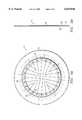
- FIG. 2is a top view of magnetron sputtering system 10 of FIG. 1.
- Backing plate 18can include conduits 19 that provide cooling channels to cool target 16 during the sputtering process.
- FIG. 2illustrates an arrangement of conduits 19 in backing plate 18 and connection of conduits 19 to coolant manifold 22.
- twelve v-shaped conduits 19, each having an input end and an output endare divided into eight groups which can include four input and four output groups.
- collector region 74 and collector region 76collect opposite ends of three pairs of connected conduits 19.
- Collector region 74 and collector region 76can serve respectively as an inlet and as an outlet for coolant.
- a coolantcan flow into the conduits through inlet collector region 74, through the three v-shaped conduits 19, and exit through outlet collector region 76.
- two manifolds 48are positioned on either side of motor 62.
- One inlet/out manifold 48can be connected in fluid communication with each inlet collector region 74, and the other inlet/out manifold 48 can be connected in fluid communication with each outlet collector region 76. In this manner, one inlet line is used to pump coolant fluid into and one outlet line is used to pump coolant fluid out of conduits 19 in backing plate 18.
- the thickness of backing plate 18can be substantially reduced due to the decrease in the pressure differential seen by backing plate 18 and the cooling of backing plate 18 using cooling channels such as conduits 19. This provides enhancement of the operation of magnetron sputtering system 10.
- FIGS. 3A and 3Bare top and cross-sectional views of the backing plate assembly 11 comprising backing plate 18, spacer ring 23 and extender ring 24.
- spacer ring 23is constructed from ceramic
- extender ring 24is constructed from stainless steel.
- Spacer ring 23can coupled to backing plate 18 and extender ring 24 according to a bonding process that provides a secure contact to backing plate 18 and will not debond when target 16 is removed from backing plate 18.
- thermal expansion of backing plate 18 and spacer ring 23are preferably substantially similar to prevent problems caused by thermal cycling.
- Ceramic spacer ring 23insulates backing plate 18 from extender ring 24. Therefore, the entire backing plate assembly 11 can be coupled to chamber walls 12 while electrically isolating backing plate 18 from chamber walls 12.
- backing plate 18comprises a number of conduits 19.
- v-shaped conduits 19are divided into four quadrants, with each quadrant having six holes 78 connecting to three conduits 19, respectively.
- conduits 19are formed by drilling into backing plate 18 from the side. The conduits are then plugged and welded on the periphery, after which holes 78 are drilled from the top to connect to conduits 19.
- FIG. 3Bshows the interconnection of holes 78 with conduits 19.
- conduits 19are formed by cutting grooves in the top of backing plate 18 and mounting a plate over the grooves. Other suitable methods of forming conduits 19 are possible.
- the present inventionprovides a cathode design with improved vacuum integrity for diode and magnetron PVD applications with ultra-high vacuum (UHV) base pressure requirements.
- the target backing plateis bonded to an electrically insulating ceramic ring.
- the ceramic ringis also bonded to a metallic extender ring which provides a vacuum seal to the process chamber top using a vacuum metal seal, vacuum elastomer seal, or other suitable vacuum seal.
- the two bonded ceramic-to-metal junctionsare hermetically sealed for excellent vacuum integrity.
- This designisolates the backing plate 18 from the electrical ground without the use of elastomer seals between the insulator ring 23 and vacuum seal ring 25.
- the ceramic insert 23 bonded between backing plate 18 and extender ring(1) allows a metal-to-metal vacuum seal at the vacuum chamber wall 12, and (2) isolates an electrically charged backing plate from the chamber walls, both without using a weaker elastomeric insulator/seal.
- the present inventioneliminates the need for any elastomeric seals to seal the vacuum chamber while electrically isolating the backing plate from the chamber walls.
- the chamber vacuumsees the backing plate, the ceramic spacer ring, the extender ring, and the ultra-high vacuum metal seal.
- the thermal bonding or brazing process used on the target backing plate 18, spacer ring 23, and extender ring 21 structureemploys a higher temperature bonding or brazing material compared to the indium bonding process used on the backing plate 18 and the target 16 junction. This ensures a reusable composite metal/ceramic/metal backing plate assembly 11 capable of surviving many new target bonding processes.
- the UHV cathode of the present inventionis compatible with conventional cathode technology.
- the spacer ring 23can be constructed from ceramic, alumina, aluminum nitride or other suitable insulating materials.
Landscapes
- Chemical & Material Sciences (AREA)
- Engineering & Computer Science (AREA)
- Chemical Kinetics & Catalysis (AREA)
- Materials Engineering (AREA)
- Mechanical Engineering (AREA)
- Metallurgy (AREA)
- Organic Chemistry (AREA)
- Physics & Mathematics (AREA)
- Plasma & Fusion (AREA)
- Analytical Chemistry (AREA)
- Physical Vapour Deposition (AREA)
Abstract
Description
Claims (33)
Priority Applications (1)
| Application Number | Priority Date | Filing Date | Title |
|---|---|---|---|
| US08/958,877US6039848A (en) | 1995-07-10 | 1997-10-27 | Ultra-high vacuum apparatus and method for high productivity physical vapor deposition. |
Applications Claiming Priority (3)
| Application Number | Priority Date | Filing Date | Title |
|---|---|---|---|
| US98095P | 1995-07-10 | 1995-07-10 | |
| US67789396A | 1996-07-10 | 1996-07-10 | |
| US08/958,877US6039848A (en) | 1995-07-10 | 1997-10-27 | Ultra-high vacuum apparatus and method for high productivity physical vapor deposition. |
Related Parent Applications (1)
| Application Number | Title | Priority Date | Filing Date |
|---|---|---|---|
| US67789396AContinuation | 1995-07-10 | 1996-07-10 |
Publications (1)
| Publication Number | Publication Date |
|---|---|
| US6039848Atrue US6039848A (en) | 2000-03-21 |
Family
ID=26668382
Family Applications (1)
| Application Number | Title | Priority Date | Filing Date |
|---|---|---|---|
| US08/958,877Expired - LifetimeUS6039848A (en) | 1995-07-10 | 1997-10-27 | Ultra-high vacuum apparatus and method for high productivity physical vapor deposition. |
Country Status (1)
| Country | Link |
|---|---|
| US (1) | US6039848A (en) |
Cited By (21)
| Publication number | Priority date | Publication date | Assignee | Title |
|---|---|---|---|---|
| US20020103564A1 (en)* | 2000-09-20 | 2002-08-01 | John Fielden | Methods and systems for determining a composition and a thickness of a specimen |
| US20020107650A1 (en)* | 2000-09-20 | 2002-08-08 | Dan Wack | Methods and systems for determining a critical dimension and a presence of defects on a specimen |
| US6585870B1 (en) | 2000-04-28 | 2003-07-01 | Honeywell International Inc. | Physical vapor deposition targets having crystallographic orientations |
| US6673637B2 (en) | 2000-09-20 | 2004-01-06 | Kla-Tencor Technologies | Methods and systems for determining a presence of macro defects and overlay of a specimen |
| US6694284B1 (en) | 2000-09-20 | 2004-02-17 | Kla-Tencor Technologies Corp. | Methods and systems for determining at least four properties of a specimen |
| US6812045B1 (en) | 2000-09-20 | 2004-11-02 | Kla-Tencor, Inc. | Methods and systems for determining a characteristic of a specimen prior to, during, or subsequent to ion implantation |
| US20040235205A1 (en)* | 2000-09-20 | 2004-11-25 | Kla-Tencor, Inc. | Methods and systems for determining a critical dimension and overlay of a specimen |
| US6919957B2 (en) | 2000-09-20 | 2005-07-19 | Kla-Tencor Technologies Corp. | Methods and systems for determining a critical dimension, a presence of defects, and a thin film characteristic of a specimen |
| US7106425B1 (en) | 2000-09-20 | 2006-09-12 | Kla-Tencor Technologies Corp. | Methods and systems for determining a presence of defects and a thin film characteristic of a specimen |
| US7130029B2 (en) | 2000-09-20 | 2006-10-31 | Kla-Tencor Technologies Corp. | Methods and systems for determining an adhesion characteristic and a thickness of a specimen |
| US7349090B2 (en) | 2000-09-20 | 2008-03-25 | Kla-Tencor Technologies Corp. | Methods and systems for determining a property of a specimen prior to, during, or subsequent to lithography |
| US20080164146A1 (en)* | 2005-02-28 | 2008-07-10 | Tosoh Smd, Inc. | Sputtering Target with an Insulating Ring and a Gap Between the Ring and the Target |
| CN100543176C (en)* | 2006-10-14 | 2009-09-23 | 中国科学院合肥物质科学研究院 | Magnetron sputtering cathode target for ultrahigh vacuum system |
| US20130056349A1 (en)* | 2011-09-01 | 2013-03-07 | Eiji Kitagawa | Sputtering target and method of manufacturing magnetic memory using the same |
| WO2013033102A1 (en)* | 2011-09-02 | 2013-03-07 | Applied Materials, Inc. | Cooling ring for physical vapor deposition chamber target |
| US9885347B2 (en) | 2013-10-30 | 2018-02-06 | Emerson Climate Technologies, Inc. | Components for compressors having electroless coatings on wear surfaces |
| JPWO2016189809A1 (en)* | 2015-05-22 | 2018-03-01 | 株式会社アルバック | Magnetron sputtering equipment |
| EP3183744A4 (en)* | 2014-08-20 | 2018-03-14 | Honeywell International Inc. | Encapsulated composite backing plate |
| KR20210092283A (en)* | 2019-03-28 | 2021-07-23 | 제이엑스금속주식회사 | Sputtering target product and method for manufacturing remanufactured product of sputtering target product |
| US11367807B2 (en) | 2017-12-28 | 2022-06-21 | Nikkiso Co., Ltd. | Nitride semiconductor light-emitting element |
| US20240048034A1 (en)* | 2020-12-10 | 2024-02-08 | Sergey Sergeevich LAGUTIN | Rotor of an asynchronous electrical machine |
Citations (25)
| Publication number | Priority date | Publication date | Assignee | Title |
|---|---|---|---|---|
| US3944911A (en)* | 1973-06-21 | 1976-03-16 | Allmanna Svenska Elektriska Aktiebolaget | Apparatus for magnetically detecting faults in metal bodies utilizing a multiphase generator to generate a rotating field in the body |
| US4299678A (en)* | 1979-07-23 | 1981-11-10 | Spin Physics, Inc. | Magnetic target plate for use in magnetron sputtering of magnetic films |
| US4407708A (en)* | 1981-08-06 | 1983-10-04 | Eaton Corporation | Method for operating a magnetron sputtering apparatus |
| GB2125440A (en)* | 1982-07-13 | 1984-03-07 | Christopher Elphick | Tunnel magnetron for cathode sputtering |
| US4444643A (en)* | 1982-09-03 | 1984-04-24 | Gartek Systems, Inc. | Planar magnetron sputtering device |
| US4461688A (en)* | 1980-06-23 | 1984-07-24 | Vac-Tec Systems, Inc. | Magnetically enhanced sputtering device having a plurality of magnetic field sources including improved plasma trapping device and method |
| US4622122A (en)* | 1986-02-24 | 1986-11-11 | Oerlikon Buhrle U.S.A. Inc. | Planar magnetron cathode target assembly |
| US4631106A (en)* | 1984-09-19 | 1986-12-23 | Hitachi, Ltd. | Plasma processor |
| US4657654A (en)* | 1984-05-17 | 1987-04-14 | Varian Associates, Inc. | Targets for magnetron sputter device having separate confining magnetic fields to separate targets subject to separate discharges |
| US4673482A (en)* | 1985-09-26 | 1987-06-16 | Hitachi, Ltd. | Sputtering apparatus |
| JPH01177368A (en)* | 1988-01-06 | 1989-07-13 | Tokuda Seisakusho Ltd | Sputtering device |
| US4872964A (en)* | 1985-08-02 | 1989-10-10 | Fujitsu Limited | Planar magnetron sputtering apparatus and its magnetic source |
| US5079481A (en)* | 1990-08-02 | 1992-01-07 | Texas Instruments Incorporated | Plasma-assisted processing magneton with magnetic field adjustment |
| US5082542A (en)* | 1990-08-02 | 1992-01-21 | Texas Instruments Incorporated | Distributed-array magnetron-plasma processing module and method |
| US5242566A (en)* | 1990-04-23 | 1993-09-07 | Applied Materials, Inc. | Planar magnetron sputtering source enabling a controlled sputtering profile out to the target perimeter |
| US5252194A (en)* | 1990-01-26 | 1993-10-12 | Varian Associates, Inc. | Rotating sputtering apparatus for selected erosion |
| US5282947A (en)* | 1992-08-13 | 1994-02-01 | Vlsi Technology, Inc. | Magnet assembly for enhanced sputter target erosion |
| US5320728A (en)* | 1990-03-30 | 1994-06-14 | Applied Materials, Inc. | Planar magnetron sputtering source producing improved coating thickness uniformity, step coverage and step coverage uniformity |
| US5328585A (en)* | 1992-12-11 | 1994-07-12 | Photran Corporation | Linear planar-magnetron sputtering apparatus with reciprocating magnet-array |
| US5354443A (en)* | 1992-07-31 | 1994-10-11 | Texas Instruments Incorporated | Method and apparatus for physical-vapor deposition of material layers |
| US5367606A (en)* | 1992-04-16 | 1994-11-22 | Texas Instruments Incorporated | Multi-zone illuminator with embedded process control sensors |
| EP0654543A2 (en)* | 1993-11-24 | 1995-05-24 | Applied Materials, Inc. | Integrated sputtering target assembly |
| US5433835A (en)* | 1993-11-24 | 1995-07-18 | Applied Materials, Inc. | Sputtering device and target with cover to hold cooling fluid |
| US5446825A (en)* | 1991-04-24 | 1995-08-29 | Texas Instruments Incorporated | High performance multi-zone illuminator module for semiconductor wafer processing |
| US5538609A (en)* | 1994-07-23 | 1996-07-23 | Leybold Aktiengesellschaft | Cathodic sputtering system |
- 1997
- 1997-10-27USUS08/958,877patent/US6039848A/ennot_activeExpired - Lifetime
Patent Citations (26)
| Publication number | Priority date | Publication date | Assignee | Title |
|---|---|---|---|---|
| US3944911A (en)* | 1973-06-21 | 1976-03-16 | Allmanna Svenska Elektriska Aktiebolaget | Apparatus for magnetically detecting faults in metal bodies utilizing a multiphase generator to generate a rotating field in the body |
| US4299678A (en)* | 1979-07-23 | 1981-11-10 | Spin Physics, Inc. | Magnetic target plate for use in magnetron sputtering of magnetic films |
| US4461688A (en)* | 1980-06-23 | 1984-07-24 | Vac-Tec Systems, Inc. | Magnetically enhanced sputtering device having a plurality of magnetic field sources including improved plasma trapping device and method |
| US4407708A (en)* | 1981-08-06 | 1983-10-04 | Eaton Corporation | Method for operating a magnetron sputtering apparatus |
| GB2125440A (en)* | 1982-07-13 | 1984-03-07 | Christopher Elphick | Tunnel magnetron for cathode sputtering |
| US4444643A (en)* | 1982-09-03 | 1984-04-24 | Gartek Systems, Inc. | Planar magnetron sputtering device |
| US4657654A (en)* | 1984-05-17 | 1987-04-14 | Varian Associates, Inc. | Targets for magnetron sputter device having separate confining magnetic fields to separate targets subject to separate discharges |
| US4631106A (en)* | 1984-09-19 | 1986-12-23 | Hitachi, Ltd. | Plasma processor |
| US4872964A (en)* | 1985-08-02 | 1989-10-10 | Fujitsu Limited | Planar magnetron sputtering apparatus and its magnetic source |
| US4673482A (en)* | 1985-09-26 | 1987-06-16 | Hitachi, Ltd. | Sputtering apparatus |
| US4622122A (en)* | 1986-02-24 | 1986-11-11 | Oerlikon Buhrle U.S.A. Inc. | Planar magnetron cathode target assembly |
| JPH01177368A (en)* | 1988-01-06 | 1989-07-13 | Tokuda Seisakusho Ltd | Sputtering device |
| US5252194A (en)* | 1990-01-26 | 1993-10-12 | Varian Associates, Inc. | Rotating sputtering apparatus for selected erosion |
| US5320728A (en)* | 1990-03-30 | 1994-06-14 | Applied Materials, Inc. | Planar magnetron sputtering source producing improved coating thickness uniformity, step coverage and step coverage uniformity |
| US5242566A (en)* | 1990-04-23 | 1993-09-07 | Applied Materials, Inc. | Planar magnetron sputtering source enabling a controlled sputtering profile out to the target perimeter |
| US5079481A (en)* | 1990-08-02 | 1992-01-07 | Texas Instruments Incorporated | Plasma-assisted processing magneton with magnetic field adjustment |
| US5082542A (en)* | 1990-08-02 | 1992-01-21 | Texas Instruments Incorporated | Distributed-array magnetron-plasma processing module and method |
| US5446825A (en)* | 1991-04-24 | 1995-08-29 | Texas Instruments Incorporated | High performance multi-zone illuminator module for semiconductor wafer processing |
| US5367606A (en)* | 1992-04-16 | 1994-11-22 | Texas Instruments Incorporated | Multi-zone illuminator with embedded process control sensors |
| US5354443A (en)* | 1992-07-31 | 1994-10-11 | Texas Instruments Incorporated | Method and apparatus for physical-vapor deposition of material layers |
| US5282947A (en)* | 1992-08-13 | 1994-02-01 | Vlsi Technology, Inc. | Magnet assembly for enhanced sputter target erosion |
| US5328585A (en)* | 1992-12-11 | 1994-07-12 | Photran Corporation | Linear planar-magnetron sputtering apparatus with reciprocating magnet-array |
| EP0654543A2 (en)* | 1993-11-24 | 1995-05-24 | Applied Materials, Inc. | Integrated sputtering target assembly |
| US5433835A (en)* | 1993-11-24 | 1995-07-18 | Applied Materials, Inc. | Sputtering device and target with cover to hold cooling fluid |
| US5433835B1 (en)* | 1993-11-24 | 1997-05-20 | Applied Materials Inc | Sputtering device and target with cover to hold cooling fluid |
| US5538609A (en)* | 1994-07-23 | 1996-07-23 | Leybold Aktiengesellschaft | Cathodic sputtering system |
Non-Patent Citations (2)
| Title |
|---|
| PCT International Search Report, Mailing Date Dec. 12, 1996.* |
| PCT International Search Report; Mailing Date Dec. 31, 1996.* |
Cited By (52)
| Publication number | Priority date | Publication date | Assignee | Title |
|---|---|---|---|---|
| US6585870B1 (en) | 2000-04-28 | 2003-07-01 | Honeywell International Inc. | Physical vapor deposition targets having crystallographic orientations |
| US20060072807A1 (en)* | 2000-09-20 | 2006-04-06 | Kla-Tencor Technologies. | Methods and systems for determining a presence of macro and micro defects on a specimen |
| US6891610B2 (en) | 2000-09-20 | 2005-05-10 | Kla-Tencor Technologies Corp. | Methods and systems for determining an implant characteristic and a presence of defects on a specimen |
| US20020179864A1 (en)* | 2000-09-20 | 2002-12-05 | John Fielden | Methods and systems for determining a thin film characteristic and an electrical property of a specimen |
| US20020179867A1 (en)* | 2000-09-20 | 2002-12-05 | John Fielden | Methods and systems for determining flatness, a presence of defects, and a thin film characteristic of a specimen |
| US20020190207A1 (en)* | 2000-09-20 | 2002-12-19 | Ady Levy | Methods and systems for determining a characteristic of micro defects on a specimen |
| US6633831B2 (en) | 2000-09-20 | 2003-10-14 | Kla Tencor Technologies | Methods and systems for determining a critical dimension and a thin film characteristic of a specimen |
| US6673637B2 (en) | 2000-09-20 | 2004-01-06 | Kla-Tencor Technologies | Methods and systems for determining a presence of macro defects and overlay of a specimen |
| US6694284B1 (en) | 2000-09-20 | 2004-02-17 | Kla-Tencor Technologies Corp. | Methods and systems for determining at least four properties of a specimen |
| US20040073398A1 (en)* | 2000-09-20 | 2004-04-15 | Kla-Tencor, Inc. | Methods and systems for determining a critical dimension and a thin film characteristic of a specimen |
| US20040092045A1 (en)* | 2000-09-20 | 2004-05-13 | Gary Bultman | Methods and systems for determining a presence of macro and micro defects on a specimen |
| US20040115843A1 (en)* | 2000-09-20 | 2004-06-17 | Kla-Tencor, Inc. | Methods and systems for determining a presence of macro defects and overlay of a specimen |
| US6782337B2 (en) | 2000-09-20 | 2004-08-24 | Kla-Tencor Technologies Corp. | Methods and systems for determining a critical dimension an a presence of defects on a specimen |
| US6806951B2 (en) | 2000-09-20 | 2004-10-19 | Kla-Tencor Technologies Corp. | Methods and systems for determining at least one characteristic of defects on at least two sides of a specimen |
| US6812045B1 (en) | 2000-09-20 | 2004-11-02 | Kla-Tencor, Inc. | Methods and systems for determining a characteristic of a specimen prior to, during, or subsequent to ion implantation |
| US6818459B2 (en) | 2000-09-20 | 2004-11-16 | Kla-Tencor Technologies Corp. | Methods and systems for determining a presence of macro defects and overlay of a specimen |
| US20040235205A1 (en)* | 2000-09-20 | 2004-11-25 | Kla-Tencor, Inc. | Methods and systems for determining a critical dimension and overlay of a specimen |
| US6829559B2 (en) | 2000-09-20 | 2004-12-07 | K.L.A.-Tencor Technologies | Methods and systems for determining a presence of macro and micro defects on a specimen |
| US7106425B1 (en) | 2000-09-20 | 2006-09-12 | Kla-Tencor Technologies Corp. | Methods and systems for determining a presence of defects and a thin film characteristic of a specimen |
| US6891627B1 (en) | 2000-09-20 | 2005-05-10 | Kla-Tencor Technologies Corp. | Methods and systems for determining a critical dimension and overlay of a specimen |
| US6917433B2 (en) | 2000-09-20 | 2005-07-12 | Kla-Tencor Technologies Corp. | Methods and systems for determining a property of a specimen prior to, during, or subsequent to an etch process |
| US6917419B2 (en) | 2000-09-20 | 2005-07-12 | Kla-Tencor Technologies Corp. | Methods and systems for determining flatness, a presence of defects, and a thin film characteristic of a specimen |
| US6919957B2 (en) | 2000-09-20 | 2005-07-19 | Kla-Tencor Technologies Corp. | Methods and systems for determining a critical dimension, a presence of defects, and a thin film characteristic of a specimen |
| US6946394B2 (en) | 2000-09-20 | 2005-09-20 | Kla-Tencor Technologies | Methods and systems for determining a characteristic of a layer formed on a specimen by a deposition process |
| US6950196B2 (en) | 2000-09-20 | 2005-09-27 | Kla-Tencor Technologies Corp. | Methods and systems for determining a thickness of a structure on a specimen and at least one additional property of the specimen |
| US20020107650A1 (en)* | 2000-09-20 | 2002-08-08 | Dan Wack | Methods and systems for determining a critical dimension and a presence of defects on a specimen |
| US20020103564A1 (en)* | 2000-09-20 | 2002-08-01 | John Fielden | Methods and systems for determining a composition and a thickness of a specimen |
| US7006235B2 (en) | 2000-09-20 | 2006-02-28 | Kla-Tencor Technologies Corp. | Methods and systems for determining overlay and flatness of a specimen |
| US7130029B2 (en) | 2000-09-20 | 2006-10-31 | Kla-Tencor Technologies Corp. | Methods and systems for determining an adhesion characteristic and a thickness of a specimen |
| US7139083B2 (en) | 2000-09-20 | 2006-11-21 | Kla-Tencor Technologies Corp. | Methods and systems for determining a composition and a thickness of a specimen |
| US7196782B2 (en) | 2000-09-20 | 2007-03-27 | Kla-Tencor Technologies Corp. | Methods and systems for determining a thin film characteristic and an electrical property of a specimen |
| US7349090B2 (en) | 2000-09-20 | 2008-03-25 | Kla-Tencor Technologies Corp. | Methods and systems for determining a property of a specimen prior to, during, or subsequent to lithography |
| US7460981B2 (en) | 2000-09-20 | 2008-12-02 | Kla-Tencor Technologies Corp. | Methods and systems for determining a presence of macro and micro defects on a specimen |
| US7751046B2 (en) | 2000-09-20 | 2010-07-06 | Kla-Tencor Technologies Corp. | Methods and systems for determining a critical dimension and overlay of a specimen |
| US8179530B2 (en) | 2000-09-20 | 2012-05-15 | Kla-Tencor Technologies Corp. | Methods and systems for determining a critical dimension and overlay of a specimen |
| US8502979B2 (en) | 2000-09-20 | 2013-08-06 | Kla-Tencor Technologies Corp. | Methods and systems for determining a critical dimension and overlay of a specimen |
| US20080164146A1 (en)* | 2005-02-28 | 2008-07-10 | Tosoh Smd, Inc. | Sputtering Target with an Insulating Ring and a Gap Between the Ring and the Target |
| US7922881B2 (en) | 2005-02-28 | 2011-04-12 | Tosoh Smd, Inc. | Sputtering target with an insulating ring and a gap between the ring and the target |
| US20110139614A1 (en)* | 2005-02-28 | 2011-06-16 | Tosoh Smd, Inc. | Sputtering target with an insulating ring and a gap between the ring and the target |
| CN100543176C (en)* | 2006-10-14 | 2009-09-23 | 中国科学院合肥物质科学研究院 | Magnetron sputtering cathode target for ultrahigh vacuum system |
| US20130056349A1 (en)* | 2011-09-01 | 2013-03-07 | Eiji Kitagawa | Sputtering target and method of manufacturing magnetic memory using the same |
| WO2013033102A1 (en)* | 2011-09-02 | 2013-03-07 | Applied Materials, Inc. | Cooling ring for physical vapor deposition chamber target |
| US9096927B2 (en) | 2011-09-02 | 2015-08-04 | Applied Materials, Inc. | Cooling ring for physical vapor deposition chamber target |
| US9885347B2 (en) | 2013-10-30 | 2018-02-06 | Emerson Climate Technologies, Inc. | Components for compressors having electroless coatings on wear surfaces |
| EP3183744A4 (en)* | 2014-08-20 | 2018-03-14 | Honeywell International Inc. | Encapsulated composite backing plate |
| JPWO2016189809A1 (en)* | 2015-05-22 | 2018-03-01 | 株式会社アルバック | Magnetron sputtering equipment |
| US11367807B2 (en) | 2017-12-28 | 2022-06-21 | Nikkiso Co., Ltd. | Nitride semiconductor light-emitting element |
| KR20210092283A (en)* | 2019-03-28 | 2021-07-23 | 제이엑스금속주식회사 | Sputtering target product and method for manufacturing remanufactured product of sputtering target product |
| JPWO2020195030A1 (en)* | 2019-03-28 | 2021-09-13 | Jx金属株式会社 | Sputtering target products and methods for manufacturing recycled products of sputtering target products |
| JP2022180456A (en)* | 2019-03-28 | 2022-12-06 | Jx金属株式会社 | Sputtering target product and method for manufacturing recycled sputtering target product |
| US12054822B2 (en) | 2019-03-28 | 2024-08-06 | Jx Advanced Metals Corporation | Sputtering target product and method for producing recycled sputtering target product |
| US20240048034A1 (en)* | 2020-12-10 | 2024-02-08 | Sergey Sergeevich LAGUTIN | Rotor of an asynchronous electrical machine |
Similar Documents
| Publication | Publication Date | Title |
|---|---|---|
| US6039848A (en) | Ultra-high vacuum apparatus and method for high productivity physical vapor deposition. | |
| US5876573A (en) | High magnetic flux cathode apparatus and method for high productivity physical-vapor deposition | |
| US6221217B1 (en) | Physical vapor deposition system having reduced thickness backing plate | |
| US5637279A (en) | Ozone and other reactive gas generator cell and system | |
| US6203620B1 (en) | Hermetically-sealed inductively-coupled plasma source structure and method of use | |
| US6378600B1 (en) | Thermally conductive chuck with thermally separated sealing structures | |
| US5846883A (en) | Method for multi-zone high-density inductively-coupled plasma generation | |
| US6488822B1 (en) | Segmented-target ionized physical-vapor deposition apparatus and method of operation | |
| JP3959273B2 (en) | Ionized physical vapor deposition method and apparatus | |
| US5985115A (en) | Internally cooled target assembly for magnetron sputtering | |
| US6907924B2 (en) | Thermally conductive chuck for vacuum processor | |
| JP3029380B2 (en) | Integrated sputtering target assembly | |
| JP5506132B2 (en) | Controllable target cooling | |
| US9127352B2 (en) | Cylindrical sputtering target, and method for manufacturing same | |
| CN109338317B (en) | Target cooling for Physical Vapor Deposition (PVD) processing systems | |
| US20070295596A1 (en) | Pvd target | |
| EP0900475A1 (en) | Electrostatic chuck | |
| CN117856497B (en) | Motor stator device and vacuum motor | |
| US4592557A (en) | Liquid cooled rotating seals | |
| WO1998002597A1 (en) | Sputtering device and liquid-cooled target assembly therefor | |
| EP0780487A1 (en) | Gasketed target assembly | |
| US3849283A (en) | Sputtering apparatus | |
| US5575856A (en) | Thermal cycle resistant seal and method of sealing for use with semiconductor wafer processing apparatus | |
| US6244210B1 (en) | Strength coil for ionized copper plasma deposition | |
| US10115574B2 (en) | Hermetically sealed magnetic keeper cathode |
Legal Events
| Date | Code | Title | Description |
|---|---|---|---|
| AS | Assignment | Owner name:MANUFACTURERS & TRADERS TRUST COMPANY, NEW YORK Free format text:SECURITY AGREEMENT;ASSIGNORS:CVC PRODUCTS, INC.;CVC, INC.;REEL/FRAME:009123/0180 Effective date:19980414 | |
| AS | Assignment | Owner name:MANUFACTURERS AND TRADERS TRUST COMPANY, NEW YORK Free format text:SECURITY AGREEMENT;ASSIGNORS:CVC PRODUCTS, INC.;CVC, INC.;REEL/FRAME:010648/0548 Effective date:19990922 | |
| STCF | Information on status: patent grant | Free format text:PATENTED CASE | |
| FEPP | Fee payment procedure | Free format text:PAT HOLDER NO LONGER CLAIMS SMALL ENTITY STATUS, ENTITY STATUS SET TO UNDISCOUNTED (ORIGINAL EVENT CODE: STOL); ENTITY STATUS OF PATENT OWNER: LARGE ENTITY | |
| REFU | Refund | Free format text:REFUND - SURCHARGE, PETITION TO ACCEPT PYMT AFTER EXP, UNINTENTIONAL (ORIGINAL EVENT CODE: R2551); ENTITY STATUS OF PATENT OWNER: LARGE ENTITY | |
| FPAY | Fee payment | Year of fee payment:4 | |
| FPAY | Fee payment | Year of fee payment:8 | |
| FEPP | Fee payment procedure | Free format text:PAYOR NUMBER ASSIGNED (ORIGINAL EVENT CODE: ASPN); ENTITY STATUS OF PATENT OWNER: LARGE ENTITY Free format text:PAYER NUMBER DE-ASSIGNED (ORIGINAL EVENT CODE: RMPN); ENTITY STATUS OF PATENT OWNER: LARGE ENTITY | |
| FPAY | Fee payment | Year of fee payment:12 |