US6039803A - Utilization of miscut substrates to improve relaxed graded silicon-germanium and germanium layers on silicon - Google Patents
Utilization of miscut substrates to improve relaxed graded silicon-germanium and germanium layers on siliconDownload PDFInfo
- Publication number
- US6039803A US6039803AUS08/806,741US80674197AUS6039803AUS 6039803 AUS6039803 AUS 6039803AUS 80674197 AUS80674197 AUS 80674197AUS 6039803 AUS6039803 AUS 6039803A
- Authority
- US
- United States
- Prior art keywords
- dislocation
- semiconductor material
- substrate
- graded
- dislocations
- Prior art date
- Legal status (The legal status is an assumption and is not a legal conclusion. Google has not performed a legal analysis and makes no representation as to the accuracy of the status listed.)
- Expired - Lifetime
Links
- 239000000758substrateSubstances0.000titleclaimsabstractdescription94
- 229910052710siliconInorganic materials0.000titleclaimsdescription7
- 239000010703siliconSubstances0.000titleclaimsdescription7
- 229910052732germaniumInorganic materials0.000titledescription35
- 229910000577Silicon-germaniumInorganic materials0.000titledescription2
- GNPVGFCGXDBREM-UHFFFAOYSA-Ngermanium atomChemical compound[Ge]GNPVGFCGXDBREM-UHFFFAOYSA-N0.000titledescription2
- LEVVHYCKPQWKOP-UHFFFAOYSA-N[Si].[Ge]Chemical compound[Si].[Ge]LEVVHYCKPQWKOP-UHFFFAOYSA-N0.000title1
- 239000004065semiconductorSubstances0.000claimsabstractdescription38
- 239000000463materialSubstances0.000claimsabstractdescription32
- 238000000034methodMethods0.000claimsabstractdescription21
- 238000012545processingMethods0.000claimsabstractdescription7
- 229910021421monocrystalline siliconInorganic materials0.000claimsabstractdescription6
- 230000003746surface roughnessEffects0.000claimsdescription26
- 229910001218Gallium arsenideInorganic materials0.000claimsdescription13
- 230000007547defectEffects0.000claimsdescription13
- 230000001965increasing effectEffects0.000claimsdescription10
- XUIMIQQOPSSXEZ-UHFFFAOYSA-NSiliconChemical compound[Si]XUIMIQQOPSSXEZ-UHFFFAOYSA-N0.000claimsdescription6
- 239000000203mixtureSubstances0.000claimsdescription4
- 238000005520cutting processMethods0.000abstractdescription3
- 230000015572biosynthetic processEffects0.000description37
- 239000010408filmSubstances0.000description19
- 230000000903blocking effectEffects0.000description18
- 239000013598vectorSubstances0.000description16
- JBRZTFJDHDCESZ-UHFFFAOYSA-NAsGaChemical compound[As]#[Ga]JBRZTFJDHDCESZ-UHFFFAOYSA-N0.000description13
- 238000006243chemical reactionMethods0.000description13
- 230000000694effectsEffects0.000description12
- 238000004458analytical methodMethods0.000description9
- 230000007423decreaseEffects0.000description9
- 235000015220hamburgersNutrition0.000description9
- 235000012431wafersNutrition0.000description9
- 230000003993interactionEffects0.000description8
- 238000003917TEM imageMethods0.000description7
- 230000007246mechanismEffects0.000description7
- 238000004630atomic force microscopyMethods0.000description6
- 230000006872improvementEffects0.000description6
- 230000006911nucleationEffects0.000description6
- 238000010899nucleationMethods0.000description6
- 230000005693optoelectronicsEffects0.000description6
- 238000004627transmission electron microscopyMethods0.000description6
- 238000013459approachMethods0.000description5
- 230000002349favourable effectEffects0.000description5
- 230000008018meltingEffects0.000description5
- 238000002844meltingMethods0.000description5
- 229910045601alloyInorganic materials0.000description4
- 239000000956alloySubstances0.000description4
- 239000000872bufferSubstances0.000description4
- 238000009792diffusion processMethods0.000description4
- 230000005669field effectEffects0.000description4
- 230000037230mobilityEffects0.000description4
- 230000008569processEffects0.000description4
- 238000005482strain hardeningMethods0.000description4
- 238000000038ultrahigh vacuum chemical vapour depositionMethods0.000description4
- 229910000530Gallium indium arsenideInorganic materials0.000description3
- WCUXLLCKKVVCTQ-UHFFFAOYSA-MPotassium chlorideChemical compound[Cl-].[K+]WCUXLLCKKVVCTQ-UHFFFAOYSA-M0.000description3
- 230000002596correlated effectEffects0.000description3
- 239000013078crystalSubstances0.000description3
- 238000010894electron beam technologyMethods0.000description3
- 238000002474experimental methodMethods0.000description3
- 230000010354integrationEffects0.000description3
- 230000009467reductionEffects0.000description3
- 238000007788rougheningMethods0.000description3
- ADZWSOLPGZMUMY-UHFFFAOYSA-Msilver bromideChemical compound[Ag]BrADZWSOLPGZMUMY-UHFFFAOYSA-M0.000description3
- 239000010409thin filmSubstances0.000description3
- XKRFYHLGVUSROY-UHFFFAOYSA-NArgonChemical compound[Ar]XKRFYHLGVUSROY-UHFFFAOYSA-N0.000description2
- 238000000089atomic force micrographMethods0.000description2
- 230000004888barrier functionEffects0.000description2
- 230000008859changeEffects0.000description2
- 238000005516engineering processMethods0.000description2
- 238000001534heteroepitaxyMethods0.000description2
- 230000004044responseEffects0.000description2
- 238000012935AveragingMethods0.000description1
- 229910000927Ge alloyInorganic materials0.000description1
- 208000012868OvergrowthDiseases0.000description1
- 229910000676Si alloyInorganic materials0.000description1
- 230000002411adverseEffects0.000description1
- 229910052786argonInorganic materials0.000description1
- 230000015556catabolic processEffects0.000description1
- 238000012512characterization methodMethods0.000description1
- 239000002800charge carrierSubstances0.000description1
- 150000001875compoundsChemical class0.000description1
- 230000003412degenerative effectEffects0.000description1
- 238000006731degradation reactionMethods0.000description1
- 230000002939deleterious effectEffects0.000description1
- 238000010586diagramMethods0.000description1
- 238000009826distributionMethods0.000description1
- 230000008030eliminationEffects0.000description1
- 238000003379elimination reactionMethods0.000description1
- 238000000407epitaxyMethods0.000description1
- 230000000763evoking effectEffects0.000description1
- 230000001939inductive effectEffects0.000description1
- 238000010884ion-beam techniqueMethods0.000description1
- 229910052751metalInorganic materials0.000description1
- 239000002184metalSubstances0.000description1
- 238000004377microelectronicMethods0.000description1
- 238000001000micrographMethods0.000description1
- 238000003801millingMethods0.000description1
- 238000012986modificationMethods0.000description1
- 230000004048modificationEffects0.000description1
- 238000001451molecular beam epitaxyMethods0.000description1
- 230000007935neutral effectEffects0.000description1
- 238000000059patterningMethods0.000description1
- 238000005498polishingMethods0.000description1
- 235000011164potassium chlorideNutrition0.000description1
- 239000001103potassium chlorideSubstances0.000description1
- 230000002035prolonged effectEffects0.000description1
- 230000006798recombinationEffects0.000description1
- 238000005215recombinationMethods0.000description1
- 238000004626scanning electron microscopyMethods0.000description1
- 239000000126substanceSubstances0.000description1
Images


Classifications
- C—CHEMISTRY; METALLURGY
- C30—CRYSTAL GROWTH
- C30B—SINGLE-CRYSTAL GROWTH; UNIDIRECTIONAL SOLIDIFICATION OF EUTECTIC MATERIAL OR UNIDIRECTIONAL DEMIXING OF EUTECTOID MATERIAL; REFINING BY ZONE-MELTING OF MATERIAL; PRODUCTION OF A HOMOGENEOUS POLYCRYSTALLINE MATERIAL WITH DEFINED STRUCTURE; SINGLE CRYSTALS OR HOMOGENEOUS POLYCRYSTALLINE MATERIAL WITH DEFINED STRUCTURE; AFTER-TREATMENT OF SINGLE CRYSTALS OR A HOMOGENEOUS POLYCRYSTALLINE MATERIAL WITH DEFINED STRUCTURE; APPARATUS THEREFOR
- C30B25/00—Single-crystal growth by chemical reaction of reactive gases, e.g. chemical vapour-deposition growth
- C30B25/02—Epitaxial-layer growth
- C30B25/18—Epitaxial-layer growth characterised by the substrate
- H—ELECTRICITY
- H01—ELECTRIC ELEMENTS
- H01L—SEMICONDUCTOR DEVICES NOT COVERED BY CLASS H10
- H01L21/00—Processes or apparatus adapted for the manufacture or treatment of semiconductor or solid state devices or of parts thereof
- H01L21/02—Manufacture or treatment of semiconductor devices or of parts thereof
- H01L21/02104—Forming layers
- H01L21/02365—Forming inorganic semiconducting materials on a substrate
- H01L21/02367—Substrates
- H01L21/0237—Materials
- H01L21/02373—Group 14 semiconducting materials
- H01L21/02381—Silicon, silicon germanium, germanium
- H—ELECTRICITY
- H01—ELECTRIC ELEMENTS
- H01L—SEMICONDUCTOR DEVICES NOT COVERED BY CLASS H10
- H01L21/00—Processes or apparatus adapted for the manufacture or treatment of semiconductor or solid state devices or of parts thereof
- H01L21/02—Manufacture or treatment of semiconductor devices or of parts thereof
- H01L21/02104—Forming layers
- H01L21/02365—Forming inorganic semiconducting materials on a substrate
- H01L21/02367—Substrates
- H01L21/02433—Crystal orientation
- H—ELECTRICITY
- H01—ELECTRIC ELEMENTS
- H01L—SEMICONDUCTOR DEVICES NOT COVERED BY CLASS H10
- H01L21/00—Processes or apparatus adapted for the manufacture or treatment of semiconductor or solid state devices or of parts thereof
- H01L21/02—Manufacture or treatment of semiconductor devices or of parts thereof
- H01L21/02104—Forming layers
- H01L21/02365—Forming inorganic semiconducting materials on a substrate
- H01L21/02436—Intermediate layers between substrates and deposited layers
- H01L21/02439—Materials
- H01L21/02441—Group 14 semiconducting materials
- H01L21/0245—Silicon, silicon germanium, germanium
- H—ELECTRICITY
- H01—ELECTRIC ELEMENTS
- H01L—SEMICONDUCTOR DEVICES NOT COVERED BY CLASS H10
- H01L21/00—Processes or apparatus adapted for the manufacture or treatment of semiconductor or solid state devices or of parts thereof
- H01L21/02—Manufacture or treatment of semiconductor devices or of parts thereof
- H01L21/02104—Forming layers
- H01L21/02365—Forming inorganic semiconducting materials on a substrate
- H01L21/02436—Intermediate layers between substrates and deposited layers
- H01L21/02494—Structure
- H01L21/02496—Layer structure
- H01L21/0251—Graded layers
- H—ELECTRICITY
- H01—ELECTRIC ELEMENTS
- H01L—SEMICONDUCTOR DEVICES NOT COVERED BY CLASS H10
- H01L21/00—Processes or apparatus adapted for the manufacture or treatment of semiconductor or solid state devices or of parts thereof
- H01L21/02—Manufacture or treatment of semiconductor devices or of parts thereof
- H01L21/02104—Forming layers
- H01L21/02365—Forming inorganic semiconducting materials on a substrate
- H01L21/02518—Deposited layers
- H01L21/02521—Materials
- H01L21/02524—Group 14 semiconducting materials
- H01L21/02532—Silicon, silicon germanium, germanium
- Y—GENERAL TAGGING OF NEW TECHNOLOGICAL DEVELOPMENTS; GENERAL TAGGING OF CROSS-SECTIONAL TECHNOLOGIES SPANNING OVER SEVERAL SECTIONS OF THE IPC; TECHNICAL SUBJECTS COVERED BY FORMER USPC CROSS-REFERENCE ART COLLECTIONS [XRACs] AND DIGESTS
- Y10—TECHNICAL SUBJECTS COVERED BY FORMER USPC
- Y10S—TECHNICAL SUBJECTS COVERED BY FORMER USPC CROSS-REFERENCE ART COLLECTIONS [XRACs] AND DIGESTS
- Y10S117/00—Single-crystal, oriented-crystal, and epitaxy growth processes; non-coating apparatus therefor
- Y10S117/901—Levitation, reduced gravity, microgravity, space
- Y10S117/902—Specified orientation, shape, crystallography, or size of seed or substrate
Definitions
- Si--Gesilicon and germanium grown on Si satisfy the lattice constant requirement and have been extensively studied in the past few years.
- Si--Gesilicon and germanium grown on Si satisfy the lattice constant requirement and have been extensively studied in the past few years.
- heteroepitaxial growth of Si--Ge/Si beyond the critical thicknessgenerally results in the formation of misfit and associated threading dislocations.
- Most applicationsdo require Si--Ge layers much thicker than that imposed by the critical thickness limit and hence, a variety of techniques have been attempted to circumvent the threading dislocation problem.
- Such graded Si--Ge alloy layers grown on silicon substratescan be used to produce high speed field effect transistors (FETs) and as substrates for integration of compound semiconductor (III-V) based optoelectronic devices.
- FETsfield effect transistors
- III-Vcompound semiconductor
- the utility of the Si--Ge/Si layershas been proven in the above applications.
- By grading up to 100% Geit is possible to create a high lattice constant semiconductor substrate on a regular Si substrate.
- Such a structurecan be used for growing good quality gallium arsenide (GaAs) layers since its lattice constant is closer to Ge than Si.
- GaAsgallium arsenide
- the strain fields associated with the misfit dislocationslead to the characteristic cross hatch pattern on the epilayer surface in lattice mismatched heteroepitaxy.
- the cross hatch patternoccurs in form of trenches and ridges aligned along the two in-plane ⁇ 110> directions.
- the cross hatch patternhas been observed in graded Si--Ge/Si and other lattice-mismatched systems such as In x Ga 1-x As/GaAs, GaAsP/GaAs, GaAs/Si and Ge x Si 1-x /Si.
- this cross hatch patternis very different from the ⁇ 100> oriented "surface ripples" that are observed in thin elastically strained Si--Ge(001) epitaxial films.
- the surface ripplesgenerally have a much shorter wavelength and originate from a thermodynamic equilibrium between surface roughness and misfit-induced elastic strain.
- the root mean square (rms) roughness associated with the cross hatch patternincreases with increase in the final Ge content of the graded Si--Ge layer.
- Surface roughnesscan affect carrier mobilities, if very severe like the "surface ripples", and is undesirable for lithographic processes.
- surface roughnesscan also lead to defects such as dislocation pile-ups. Such defects adversely affect the electronic quality of the Si--Ge material and hence the device reliability. It is important to understand the origin and interactions of these defects with the surface morphology, in order to eliminate them or minimize their density.
- misfit dislocationsthat form an orthogonal array along the two in-plane ⁇ 110> directions at the hetero-interface.
- These misfit dislocationscommonly have an out-of-plane Burgers vector of the type 1/2 ⁇ 101> or 1/2 ⁇ 011>. It is known that 60° dislocations can react under favorable conditions to form edge dislocations with in-plane Burgers vectors of the type 1/2 ⁇ 110>.
- (001) silicon substratesthat are off-cut towards a ⁇ 110> direction by 6° are used in the growth of graded Si--Ge layers.
- the present inventioninvolves the use of miscut Si(001) substrates and obtained improved layer quality in terms of surface roughness and dislocation pile-up densities.
- the root mean square (rms) surface roughness measured using atomic force microscopy (AFM)shows a 75% improvement for samples graded up to 100% Ge over growth on the conventional on-axis Si(001) substrates.
- the dislocation pile-up densities measured using electron beam induced current (EBIC)were about an order of magnitude lower for the 100% Ge samples grown on the off-cut Si substrates as compared to growth on the on-axis Si substrates.
- EBICelectron beam induced current
- the reduced surface roughnesstranslates into ease of subsequent processing for GaAs growth.
- a lower surface roughnessalso helps in easy patterning of the Ge surface for device processing.
- Reduced dislocation pile-up densityimplies that the material has improved electronic properties.
- III-V optoelectronic devicessuch as light emitting diodes (LEDs), semiconductor lasers, and metal semiconductor field effect transistors (MESFETs).
- LEDslight emitting diodes
- MESFETsmetal semiconductor field effect transistors
- III-V optoelectronic deviceshave been grown on expensive GaAs substrates.
- Sicannot emit light efficiently, and therefore optoelectronics has yet to become a light-volume product. Since the silicon technology is very well established, it would be very economical to produce III-V (GaAs, GaInP) based devices and Si based circuits on the same chip.
- III-VGaAs, GaInP
- SiSi based circuits on the same chip.
- the lack of reliable way of producing good quality GaAs layers on silicon substrateshas been the biggest barrier in achieving the aforementioned integration. Growth of good quality Ge layers on Si will provide an inexpensive rout to produce III-V optoelectronic layers on Si substrates. It is quite likely that the future of the
- a method of processing semiconductor materialsincluding providing a monocrystalline substrate of a first semiconductor material having a (001) crystallographic surface orientation; off-cutting the substrate to an orientation from about 1° to about 8° offset from the [001] direction; and epitaxially growing a relaxed graded layer of a crystalline second semiconductor material on the substrate, the second semiconductor material including at least the first semiconductor material.
- a method of processing semiconductor materialsincluding providing a monocrystalline silicon substrate having a (001) crystallographic surface orientation; off-cutting the substrate to an orientation from about 2° to about 6° offset towards the [110] direction; and epitaxially growing a relaxed graded layer of a crystalline GeSi on the substrate.
- a semiconductor structureincluding a monocrystalline silicon substrate having a (001) crystallographic surface orientation, the substrate being off-cut to an orientation from about 2° to about 6° offset towards the [110] direction; and a relaxed graded layer of a crystalline GeSi which is epitaxially grown on the substrate.
- FIG. 1Ais a schematic of an exemplary sample structure 10 in accordance with the present invention.
- FIG. 1Bis a plot showing increase in threading dislocation density with increasing final Ge % in the graded layer
- FIG. 2is a plot showing the increase in rms surface roughness with increase in the final Ge % of the graded layer
- FIG. 3is an AFM image of the surface of UHVCVD grown relaxed graded Ge-Si exemplary sample graded up to 100% Ge on a Si(001) substrate;
- FIG. 4is a graph showing a plot of h/h* versus (h/b) ⁇ *, used to calculate h*/h ratio for graded Si--Ge/Si layers;
- FIG. 5is a schematic showing the gliding dislocations interacting with existing dislocations and getting blocked at the trench side-walls;
- FIG. 6is a graph showing the variation of maximum trench depth of surface cross-hatch pattern with increase in final Ge % in the graded layer
- FIG. 7is a schematic diagram illustrating the nature of interactions between surface morphology and dislocation pile-ups
- FIG. 8is a bar graph showing the correlation between the observed rms roughness and dislocation pile-up density along the two in-plane ⁇ 110> directions for Ge/Ge x Si 1-x /Si samples graded up to 100% Ge grown on the on-axis exact (001) and 6° off-cut (001) Si substrates;
- FIGS. 9A and 9Bare plan view EBIC images of Ge/Ge x Si 1-x /Si samples graded up to 100% Ge grown on Si(001) exact and Si(001) 6° off-cut towards ⁇ 110> Si substrates, respectively;
- FIG. 10is a schematic plan view of the 60° dislocation network on an on-axis substrate and a substrate off-cut towards the ⁇ 110> direction;
- FIG. 11Ais a plan view TEM micrograph showing the dislocation structure in the Si-rich graded region of a Ge/Ge x Si 1-x /Si(001) sample;
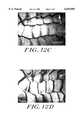
- FIG. 11Bis a plan view TEM micrograph of a novel and unexpected hexagonal dislocation structure in the Ge rich region of a similar structure as in FIG. 11A;
- FIGS. 12A to 12Dare plan view TEM micrographs showing the aforementioned analysis from the same area, but using different g beams for Burgers vector analysis of the hexagonal network to form the image.
- the present inventionis directed to the use and effect of substrate miscut on the surface morphology and the dislocation structure in Ge/Si--Ge(graded)/Si. It will be appreciated by those of skill in the art that a criterion exists for the arrest of a threading dislocation in a strained epitaxial layer due to interaction with the stress field of an orthogonal misfit dislocation lying in its path, as described in L. B. Freund, J. Appl. Phys. 68, 2073 (1990), incorporated herein by reference.
- dislocation blocking criterionto graded Si--Ge structures with a rough surface, it is possible to predict the formation of dislocation pile-ups from the maximum trench depth of the cross hatch pattern. The pile-ups are not only deleterious because they contain a high threading dislocation density, but they lead to extremely rough surfaces due to stress-related growth instability.
- edge dislocations of the type 1/2 ⁇ 110 > as well as in-plane Burgers vectors of the type ⁇ 100>have been observed.
- edge dislocations and two ⁇ 100> edge dislocationslead to a lower energy hexagonal dislocation network.
- Such a dislocation networkfirst reported in bulk silver bromide crystals, has not been previously characterized in lattice mismatched heteroepitaxial thin films.
- the present inventionsuggests that favorable intersection of the ⁇ 111 ⁇ glide planes in exemplary samples grown on the miscut substrates aid the dislocation reactions necessary to form this network.
- miscut substratesprovide a substantial improvement in the defect structure and surface morphology in Ge/Si--Ge(graded)/Si structures.
- growth on miscut substratesencourages the formation of a hexagonal dislocation structure which may relax layers with improved surface morphologies and lower defect densities.
- FIG. 1Ais a schematic of an exemplary sample structure 10 in accordance with the present invention.
- the exemplary structureincludes a (001) monocrystalline silicon substrate 12 having its crystallographic orientation off-cut to an orientation from about 1° to about 8° offset from the [001] direction, preferably having a 6° off-cut towards in-plane ⁇ 110>.
- other desired III-V semiconductor materialssuch as GaAs and GaInP can also be utilized to produce the exemplary structure.
- Exemplary epitaxial films of Ge/Ge x Si 1-x /Siwere grown on 2 inch (001) and (001) 6° off-cut (towards in-plane ⁇ 110>) n--Si substrates using ultra-high vacuum chemical vapor deposition (UHVCVD).
- a 1-2 ⁇ m uniform cap layer of pure Gewas grown above the graded region.
- the top 0.1 ⁇ m of the uniform cap layerwas p-doped to create a p-i-n structure suitable for electron beam induced current (EBIC) characterization.
- EBICelectron beam induced current
- Ge x Si 1-x /Si(001) films graded to 30% and 70% final Ge compositionwere also grown under similar growth conditions for comparison.
- the cap layer in each casehad the same uniform Ge concentration as the final Ge % in the respective graded layers.
- the surface morphology of the heterostructureswas characterized using scanning electron microscopy (SEM) and atomic force microscopy (AFM).
- SEMscanning electron microscopy
- AFMatomic force microscopy
- the rms roughness datawas obtained from a number of 100 ⁇ m ⁇ 100 ⁇ m surface scans using contact mode AFM (Nanoscope III, Digital Instruments Inc.).
- the maximum trench depth of the cross hatch patternwas determined by the "section analysis" routine.
- the dislocation structureswere characterized primarily through (001) plan view TEM.
- the samples for observationwere prepared by mechanical polishing from the Si substrate side to about 20 ⁇ m followed by argon ion beam milling.
- the samplewas ion-milled primarily from the substrate side until electron transparency was obtained.
- the samplewas milled from both the substrate side and the epilayer side.
- Electron beam inducted currentwas used to observe electrically active dislocations threading up through the uniform cap layer.
- the threading segments of dislocations gliding on the ⁇ 111 ⁇ planescan interact with stress fields of pre-existing orthogonal misfit dislocations and get trapped. Other factors like surface trenches can aid such blocking.
- This blockingcan create dislocation pile-ups along trenches in the cross hatch pattern. These pile-ups were good recombination sites for charge carriers and showed a dark contrast along the trenches.
- the dislocation pile-upsare planar defects and their densities were characterized by the number of intersections per unit length of the sample surface. The density (no./cm) was determined by calculating the number of intersections of the dark contrast lines with random straight lines drawn on the EBIC micrographs.
- FIG. 1Bis a plot showing increase in threading dislocation density with increasing final Ge % in the graded layer.
- FIG. 1shows the trend in threading dislocation density versus final Ge concentration in graded 10% Ge/ ⁇ m layers. If it is desired to integrate devices on these buffers, the origin of this dislocation increase must be determined.
- the threading dislocation density increasecan be correlated to pile-up density and surface roughness. For this constant grading rate, one does not expect an increase in threading dislocation density unless there is a decrease in average misfit dislocation length.
- dislocation interactions that arrest dislocation motionmust become more probable with thicker graded layers.
- increase in threading dislocation densitycan be correlated to surface roughness and dislocation pile-up density.
- strain in epitaxial filmsis directly correlated to surface morphology.
- the strain fields associated with threading dislocationsalso change the surface morphology.
- Lattice mismatch strain itself, without the presence of dislocations,can roughen the surface if the growth temperature, sign and magnitude of the strain is adequate.
- the unifying themeis that any event that can produce lattice strain will induce surface roughening if the temperature is high enough to allow enough surface diffusion to approach thermodynamic equilibrium.
- the surface roughness due to the cross hatch pattern in graded Si--Ge structuresis primarily due to strain fields arising from inhomogeneous distribution of misfit dislocations at each grading step interface.
- the growing surfaceincorporates undulations (to minimize strain energy) in response to local strain field variations.
- the strain field variations from an array of misfit dislocations at each hetero-interfaceextend well beyond each Ge grading step (0.33 ⁇ m).
- the cross hatch pattern at any instant during the growthis the response of the surface to multiple overlapping strain fields.
- the formation of cross hatch patternexposes higher index planes along the trenches. CVD growth subsequently leads to anisotropic growth effects and accentuates the surface roughness further.
- FIG. 2is a plot showing the increase in rms surface roughness with increase in the final Ge % of the graded layer, and shows the effect of increasing final Ge content of the graded layer on the rms roughness of the top surface in Ge x Si 1-x /Si films. Since all the graded layers were grown at 10% Ge/ ⁇ m, different final Ge contents imply that the graded regions in each structure are of different thicknesses.
- the rms roughness for each samplewas obtained by averaging the height data over several 100 ⁇ m ⁇ 100 ⁇ m surface scans, obtained by using the AFM in the contact mode. The roughness due to the cross hatch pattern was found to increase with final Ge content for samples grown on exact (001) oriented substrates. For the Ge/Ge x Si 1-x /Si samples grown on the (001) miscut substrates (6° off towards ⁇ 110>) there was a tremendous improvement in surface roughness.
- the cross hatch patterncontributes to an increase in surface roughness. It has been suggested that the cross hatch pattern is primarily due to formation of surface steps produced by gliding 60° dislocations. This proposition alone, however, does not explain the increase in rms roughness of the cross hatch pattern with increase in grading rate for equally relaxed graded SiGe structures. Nor can it explain difference in cross hatch morphology (long-wavelength surface undulations) due to growth temperature.
- FIG. 3is an AFM image of the surface of UHVCVD grown relaxed graded Ge-Si exemplary sample graded up to 100% Ge on a Si(001) substrate. Deep trenches running along the two in-plane ⁇ 110> directions account for the high rms roughness ( ⁇ 210 nm).
- FIG. 4is a graph showing a plot of h/h* versus (h/b) ⁇ *, used to calculate h*/h ratio for graded Si--Ge/Si layers.
- the different curvescorrespond to different dislocation combinations.
- h*/hFor the strains involved in the exemplary samples h*/h always tend to 1, irrespective of the dislocation combination chosen.
- FIG. 4is plot of normalized channel width, h*/h as a function of (h/b) ⁇ , where h is the height of the film.
- h*is the channel width through which a threading segment must pass to overcome the stress field of the orthogonal dislocation.
- the equilibrium critical thicknessis ⁇ 375 nm.
- the grading rate of 10% Ge/ ⁇ mwas achieved by increasing the Ge content by ⁇ 3.33% Ge in steps of ⁇ 333 nm.
- each step in Geis completely strained until the next step in concentration occurs, and the threading dislocation experiences approximately the same force as a single heterostructure 333 nm in thickness.
- the critical thicknessis a strong function of the Ge grading rate and nearly independent of the final Ge % of the graded layer. Hence, the same critical thickness approximation can be applied to films graded to different final Ge % (at the same grading rate) in the experiments.
- the background strain, ⁇ *, for all filmsis ⁇ 0.12% for a 3.33% Ge increase per step.
- the h/h* ratioapproaches unity.
- This h/h*means that the channel width, h*, is almost as thick as the epilayer.
- the gliding threading segmentcan easily overcome the strain field and blocking effect of orthogonal misfit dislocation. Therefore, the blocking criterion of a single perpendicular dislocation alone cannot explain the formation of dislocation pile-ups in graded Ge x Si 1-x /Si structures, since at 10% Ge/ ⁇ m grading rate, no blocking should occur.
- FIG. 5shows a schematic that explains the possible mechanism of dislocation pile-up formation in graded Ge x Si 1-x /Si structures.
- the figureshows a threading segment of a gliding dislocation interacting and being blocked by the stress fields of pre-existing groups of orthogonal misfit dislocations.
- groupsare known to exist in mismatch structures due to heterogeneous nucleation sources.
- the strain fields from such a groupcreate a deeper trough in the cross-hatch pattern.
- the channel width, h*can decrease to zero from both the depression in the surface morphology and the stress fields from the orthogonal dislocations.
- the channel width, h*is lesser than the film thickness, h, through which the threading segment has to pass.
- the threading segmentmight get blocked by a surface trench that is deeper than the channel width, h*, and lying right above the orthogonal misfit dislocations as shown in the schematic (which are responsible for the trench formation initially, as described previously).
- Other gliding segments traveling on the same or parallel ⁇ 111 ⁇ planescould also be blocked by the same effect, and by previous threading dislocations which have been blocked. Such an event can lead to a dislocation pile-up along the trench.
- the surface featuresare formed due to the stress fields of buried misfit dislocations groups. Not all surface trenches would be deeper than the channel width, h*. Thus, the blocking event and hence the dislocation pile-up formation is a rare event occurring only when the trench is deeper than h*. However, it is unlikely that all of the surface trenches that could lead to nucleation would be deeper than the channel width, h*. Thus, the blocking events must be responsible for dislocation pile-up formation. Using this hypothesis of dislocation blocking, estimates of when blocking should occur can be made.
- FIG. 6is a graph showing the variation of maximum trench depth of surface cross-hatch pattern with increase in final Ge % in the graded layer.
- the maximum depth of a surface trench from the cross hatch patternincreases with increase in final Ge % of the graded region as shown in FIG. 6.
- the value of h* for 10% Ge/ ⁇ m grading rateis also plotted on the same graph. It will be appreciated that h* is a function of grading rate only and not of the final Ge % of the graded region.
- dislocation pile-upscan be expected. The farther above the "maximum trench depth" point is from the h* line, the more trenches can block dislocations and hence create dislocation pile-ups.
- the dislocation pile-up formationcan affect, e.g. the degradation of, surface morphology as well. Threading segments of gliding dislocations terminate on the trench side-walls at a dislocation pile-up.
- the surface sites at or near the trench side-walls where the dislocations terminateare energetically unfavorable sites for atoms diffusing on the growth surface. This reduces the growth rate along the trench side-walls as compared to growth of the average surface. Such an effect increases the trench depths, making more gliding dislocations prone to blockage.
- the vicious nature of the interactions of the surface morphology and dislocation pile-up formationis summed up in a schematic sketch of FIG. 7.
- FIG. 8shows a graph of the correlation between the observed rms roughness and dislocation pile-up density along the two in-plane ⁇ 110> directions for Ge/Ge x Si 1-x /Si samples graded up to 100% Ge grown on the on-axis exact (001) and 6° off-cut (001) Si substrates. It was found that a high rms roughness was associated with a high dislocation pile-up density for a given direction on the sample surface.
- edge dislocationswith in-plane Burgers vectors.
- Such dislocationsdo not produce as severe strain field inhomogeneities at the growth surface as the mixed 60° dislocation.
- the strain fields from the neighboring dislocationswill quickly annihilate, thus creating less residual strain fields at the surface of the growing epilayer.
- the edge dislocationsare more easily formed on the off-cut substrate than the exact oriented one, therefore contributing to a lower rms roughness for same samples grown on off-cut substrates.
- FIGS. 9A and 9Bare plan view EBIC images of Ge/Ge x Si 1-x /Si samples graded up to 100% Ge grown on Si(001) exact and Si(001) 6° off-cut towards ⁇ 110> Si substrates, respectively.
- the imagesillustrate the drastic reduction in dislocation pile-up density for the sample grown on the off-cut substrate.
- For the sample grown on the off-cut substratethere is a clear anisotropy in the density of pile-ups along the two in-plane ⁇ 110> directions.
- the plot of FIG. 6predicts that the samples graded up to 70% Ge and 100% Ge would form dislocation pile-ups. It was found to be true for the 100% Ge samples grown on Si(001) and Si(001) off-cut substrates, as shown in FIGS. 9A and 9B. There is a substantial reduction in dislocation pile-up density in the 100% Ge sample grown on an off-cut substrate. As previously described, growth on an (001) off-cut substrate results in reduced surface roughness and reduced trench depths. In FIG. 6, the "maximum trench depth" point for the off-cut sample is close to the h* line indicating that there are only a few deep trenches that can cause dislocation blocking.
- the dislocation pile-up densityis extremely low for growth on the off-cut substrate.
- FIG. 8there was a clear anisotropy in the dislocation pile-up density along the two in-plane ⁇ 110> directions in case of the 100% Ge sample grown on an off-cut substrate.
- the anisotropy in dislocation pile-up densityis related to the anisotropy or rms roughness previously described.
- Anisotrophy in surface roughness and dislocation pile-up density of a much lesser degreeis also observed in the 100% Ge (001) exact oriented sample. This anisotrophy is probably related to unintentional miscut in the substrate.
- FIG. 10is a schematic plan view of the 60° dislocation network on an on-axis and a wafer off-cut towards the ⁇ 110> direction. Since the 60° dislocations are not parallel, a nucleation source cannot create long lines of parallel dislocations with the same Burgers vector.
- FIG. 11Ais a plan view TEM micrograph showing the dislocation structure in the Si-rich graded region of a Ge/Ge x Si 1-x /Si(001) sample. An array of primarily 60° dislocations running along the two in-plane orthogonal ⁇ 110> directions was observed.
- FIG. 11Bis a plan view TEM micrograph of a novel and unexpected hexagonal dislocation structure in the Ge rich region of a similar structure as in FIG. 11A. The array of 60° dislocations, which formed initially, reacted to form a lower energy hexagonal network of dislocations. A "g.b" analysis of the dislocation structure in FIG. 11B was performed to determine the Burgers vectors of the dislocations that made up the hexagonal network.
- FIGS. 12A to 12Dare plan view TEM micrographs showing the aforementioned analysis from the same area, but using different g beams for Burgers vector analysis of the hexagonal network to form the image. It was found that the entire hexagonal network was made up of dislocations with in-plane Burgers vectors of the type 1/2 ⁇ 110>, 1/2 ⁇ 110>and ⁇ 100>.
- FIG. 12A g040
- FIG. 12B g400
- FIG. 12C g220
- FIG. 12D g-220.
- FIG. 11Ashows one such array of 60° dislocations existing in a (001) interface in the Si-rich region of the graded Si--Ge structure.
- FIG. 11Bshows a similar TEM micrograph taken from the Ge-rich region of the graded structure grown on a (001) off-cut substrate. A hexagonal network of dislocations is observed. A "g.b" analysis of the network in FIG.
- FIGS. 12A-12Drevealed that it was made up of dislocations of the type 1/2 ⁇ 110>, 1/2 ⁇ 110> and ⁇ 100>.
- Each node in the hexagonal networkis formed by a ⁇ 110> edge type dislocation and two reacting 1/2 ⁇ 110> edges.
- Such dislocation networkshave also been observed in bulk silver bromide (AgBr) and potassium chloride (KCI) crystals. To date, such a dislocation structure has not been observed in heteroepitaxial thin film growth.
- the off-cut of the substrateincreases the probability that a 60° dislocation would find the right 60° to react with.
- 1/2 ⁇ 110> types edge dislocationsit would be easier for the 1/2 ⁇ 110> types edge dislocations to form.
- the presence of more 1/2 ⁇ 110> type edge dislocationsimplies that more reactions as shown in equations (1) and (2) could occur, and hence it is easier to form the low energy hexagonal network of dislocations.
- the formation of 1/2 ⁇ 110> type edgesis more difficult, and hence formation of ⁇ 110> dislocations is more difficult.
- the new dislocation structureoffers new degrees of freedom in designing relaxation processes.
- the 60° dislocationsare advantageous, since their introduction can be controlled at relatively low temperatures.
- dislocation pile-up formation and surface roughness in graded Ge/Ge x Si 1-x /Si layershas been investigated.
- the effect of substrate off-cut on surface morphology, dislocation pile-up formation and the dislocation structurewas studied as well.
- Dislocation pile-upsoriginate from a combination of dislocation interaction and the effect of surface morphology.
- the exemplary samples grown on (001) off-cut substratesshowed reduced surface roughness and a low dislocation pile-up density as compared to samples grown on (001) exact oriented substrates.
- a modelwas proposed to explain the formation of dislocation pile-ups in graded structures.
- the atomic mobility in the Ge-rich alloysis higher since the growth temperature is closer to the melting point. This facilities the dislocation climb reactions necessary for the hexagonal network formation.
- favorable intersections of the right kinds 60° dislocationsaided the formation of 1/2 ⁇ 110> type edge dislocations, and hence the ⁇ 110> type as compared to exact oriented samples.
- the new dislocation structuresoffer to explore new processes which may eliminate spatially variant strain fields in relaxed epitaxial layers and reduce threading dislocation densities.
Landscapes
- Engineering & Computer Science (AREA)
- Physics & Mathematics (AREA)
- Condensed Matter Physics & Semiconductors (AREA)
- General Physics & Mathematics (AREA)
- Manufacturing & Machinery (AREA)
- Computer Hardware Design (AREA)
- Microelectronics & Electronic Packaging (AREA)
- Power Engineering (AREA)
- Chemical & Material Sciences (AREA)
- Crystallography & Structural Chemistry (AREA)
- Materials Engineering (AREA)
- Chemical Kinetics & Catalysis (AREA)
- General Chemical & Material Sciences (AREA)
- Metallurgy (AREA)
- Organic Chemistry (AREA)
- Recrystallisation Techniques (AREA)
Abstract
Description
Claims (13)
Priority Applications (2)
| Application Number | Priority Date | Filing Date | Title |
|---|---|---|---|
| US08/806,741US6039803A (en) | 1996-06-28 | 1997-02-27 | Utilization of miscut substrates to improve relaxed graded silicon-germanium and germanium layers on silicon |
| PCT/US1997/010765WO1998000857A1 (en) | 1996-06-28 | 1997-06-20 | Utilization of miscut substrates to improve relaxed graded silicon-germanium and germanium layers on silicon |
Applications Claiming Priority (2)
| Application Number | Priority Date | Filing Date | Title |
|---|---|---|---|
| US2082096P | 1996-06-28 | 1996-06-28 | |
| US08/806,741US6039803A (en) | 1996-06-28 | 1997-02-27 | Utilization of miscut substrates to improve relaxed graded silicon-germanium and germanium layers on silicon |
Publications (1)
| Publication Number | Publication Date |
|---|---|
| US6039803Atrue US6039803A (en) | 2000-03-21 |
Family
ID=26693916
Family Applications (1)
| Application Number | Title | Priority Date | Filing Date |
|---|---|---|---|
| US08/806,741Expired - LifetimeUS6039803A (en) | 1996-06-28 | 1997-02-27 | Utilization of miscut substrates to improve relaxed graded silicon-germanium and germanium layers on silicon |
Country Status (2)
| Country | Link |
|---|---|
| US (1) | US6039803A (en) |
| WO (1) | WO1998000857A1 (en) |
Cited By (73)
| Publication number | Priority date | Publication date | Assignee | Title |
|---|---|---|---|---|
| WO2002082513A1 (en)* | 2001-04-02 | 2002-10-17 | Motorola, Inc. | Semiconductor structures and devices utilizing a stable template |
| WO2002082551A1 (en)* | 2001-04-02 | 2002-10-17 | Motorola, Inc. | A semiconductor structure exhibiting reduced leakage current |
| WO2002086201A1 (en)* | 2001-04-19 | 2002-10-31 | Motorola, Inc., A Corporation Of The State Of Delaware | Semiconductor structures and devices utilizing perovskite stacks |
| US6515335B1 (en)* | 2002-01-04 | 2003-02-04 | International Business Machines Corporation | Method for fabrication of relaxed SiGe buffer layers on silicon-on-insulators and structures containing the same |
| US20030036217A1 (en)* | 2001-08-16 | 2003-02-20 | Motorola, Inc. | Microcavity semiconductor laser coupled to a waveguide |
| US20030113948A1 (en)* | 2000-01-20 | 2003-06-19 | Amberwave Systems Corporation | Low threading dislocation density relaxed mismatched epilayers without high temperature growth |
| US20030126525A1 (en)* | 2001-12-06 | 2003-07-03 | Koji Miyashita | Semiconductor device, method of testing the same and electronic instrument |
| US6589856B2 (en) | 2001-08-06 | 2003-07-08 | Motorola, Inc. | Method and apparatus for controlling anti-phase domains in semiconductor structures and devices |
| US6589335B2 (en)* | 2001-02-08 | 2003-07-08 | Amberwave Systems Corporation | Relaxed InxGa1-xAs layers integrated with Si |
| US6594293B1 (en)* | 2001-02-08 | 2003-07-15 | Amberwave Systems Corporation | Relaxed InxGa1-xAs layers integrated with Si |
| US6600170B1 (en) | 2001-12-17 | 2003-07-29 | Advanced Micro Devices, Inc. | CMOS with strained silicon channel NMOS and silicon germanium channel PMOS |
| US6617060B2 (en) | 2000-12-14 | 2003-09-09 | Nitronex Corporation | Gallium nitride materials and methods |
| US6639249B2 (en) | 2001-08-06 | 2003-10-28 | Motorola, Inc. | Structure and method for fabrication for a solid-state lighting device |
| US6638838B1 (en) | 2000-10-02 | 2003-10-28 | Motorola, Inc. | Semiconductor structure including a partially annealed layer and method of forming the same |
| US6642536B1 (en) | 2001-12-17 | 2003-11-04 | Advanced Micro Devices, Inc. | Hybrid silicon on insulator/bulk strained silicon technology |
| US20030207589A1 (en)* | 2002-05-03 | 2003-11-06 | Thoughtbeam, Inc. | Method for growing a monocrystalline oxide layer and for fabricating a semiconductor device on a monocrystalline substrate |
| US6646293B2 (en) | 2001-07-18 | 2003-11-11 | Motorola, Inc. | Structure for fabricating high electron mobility transistors utilizing the formation of complaint substrates |
| US6667196B2 (en) | 2001-07-25 | 2003-12-23 | Motorola, Inc. | Method for real-time monitoring and controlling perovskite oxide film growth and semiconductor structure formed using the method |
| US6673646B2 (en) | 2001-02-28 | 2004-01-06 | Motorola, Inc. | Growth of compound semiconductor structures on patterned oxide films and process for fabricating same |
| US6673667B2 (en) | 2001-08-15 | 2004-01-06 | Motorola, Inc. | Method for manufacturing a substantially integral monolithic apparatus including a plurality of semiconductor materials |
| FR2842217A1 (en)* | 2002-07-12 | 2004-01-16 | St Microelectronics Sa | GROWTH OF A MONOCRYSTALLINE REGION OF A III-V COMPOUND ON A MONOCRYSTALLINE SILICON SUBSTRATE |
| US6689671B1 (en) | 2002-05-22 | 2004-02-10 | Advanced Micro Devices, Inc. | Low temperature solid-phase epitaxy fabrication process for MOS devices built on strained semiconductor substrate |
| US6693298B2 (en) | 2001-07-20 | 2004-02-17 | Motorola, Inc. | Structure and method for fabricating epitaxial semiconductor on insulator (SOI) structures and devices utilizing the formation of a compliant substrate for materials used to form same |
| US6693033B2 (en) | 2000-02-10 | 2004-02-17 | Motorola, Inc. | Method of removing an amorphous oxide from a monocrystalline surface |
| US20040040493A1 (en)* | 2002-08-30 | 2004-03-04 | Amberwave Systems Corporation | Reduction of dislocation pile-up formation during relaxed lattice-mismatched epitaxy |
| US6709989B2 (en) | 2001-06-21 | 2004-03-23 | Motorola, Inc. | Method for fabricating a semiconductor structure including a metal oxide interface with silicon |
| US20040067644A1 (en)* | 2002-10-04 | 2004-04-08 | Malik Igor J. | Non-contact etch annealing of strained layers |
| US6723622B2 (en) | 2002-02-21 | 2004-04-20 | Intel Corporation | Method of forming a germanium film on a semiconductor substrate that includes the formation of a graded silicon-germanium buffer layer prior to the formation of a germanium layer |
| US20040075105A1 (en)* | 2002-08-23 | 2004-04-22 | Amberwave Systems Corporation | Semiconductor heterostructures having reduced dislocation pile-ups and related methods |
| US20040137735A1 (en)* | 2002-11-19 | 2004-07-15 | Nagoya University | Method for fabricating a SiGe film, substrate for epitaxial growth and multilayered structure |
| US20040150006A1 (en)* | 2003-01-29 | 2004-08-05 | Cecile Aulnette | Semiconductor structure for providing strained crystalline layer on insulator and method for fabricating same |
| US6787423B1 (en) | 2002-12-09 | 2004-09-07 | Advanced Micro Devices, Inc. | Strained-silicon semiconductor device |
| WO2004082001A1 (en)* | 2003-03-10 | 2004-09-23 | Forschungszentrum Jülich GmbH | Method for the production of stress-relaxed layer structure on a non-lattice adapted substrate and utilization of said layer system in electronic and/or optoelectronic components |
| US20040224469A1 (en)* | 2003-05-08 | 2004-11-11 | The Board Of Trustees Of The University Of Illinois | Method for forming a strained semiconductor substrate |
| US20040232525A1 (en)* | 2000-02-10 | 2004-11-25 | Motorola, Inc. | Semiconductor structure, semiconductor device, communicating device, integrated circuit, and process for fabricating the same |
| US20040262631A1 (en)* | 1997-06-24 | 2004-12-30 | Massachusetts Institute Of Technology | Controlling threading dislocation densities in Ge on Si using graded GeSi layers and planarization |
| US20050023576A1 (en)* | 2003-07-31 | 2005-02-03 | Wen-Chin Lee | Semiconductor structure having a strained region and a method of fabricating same |
| US6852588B1 (en) | 2004-06-30 | 2005-02-08 | Freescale Semiconductor, Inc. | Methods of fabricating semiconductor structures comprising epitaxial Hf3Si2 layers |
| US6855992B2 (en) | 2001-07-24 | 2005-02-15 | Motorola Inc. | Structure and method for fabricating configurable transistor devices utilizing the formation of a compliant substrate for materials used to form the same |
| US20050066886A1 (en)* | 2003-09-26 | 2005-03-31 | Takeshi Akatsu | Method of fabrication of a substrate for an epitaxial growth |
| US6885065B2 (en) | 2002-11-20 | 2005-04-26 | Freescale Semiconductor, Inc. | Ferromagnetic semiconductor structure and method for forming the same |
| US20050139961A1 (en)* | 2003-12-25 | 2005-06-30 | Siltronic Ag | Semiconductor substrate and method for production thereof |
| US20050164477A1 (en)* | 2003-09-23 | 2005-07-28 | Dureseti Chidambarrao | Strained silicon on relaxed sige film with uniform misfit dislocation density |
| US20050181549A1 (en)* | 2004-02-17 | 2005-08-18 | Barr Alexander L. | Semiconductor structure having strained semiconductor and method therefor |
| US6965128B2 (en) | 2003-02-03 | 2005-11-15 | Freescale Semiconductor, Inc. | Structure and method for fabricating semiconductor microresonator devices |
| US20050277278A1 (en)* | 2004-06-11 | 2005-12-15 | Christophe Maleville | Method of manufacturing a wafer |
| US6992321B2 (en) | 2001-07-13 | 2006-01-31 | Motorola, Inc. | Structure and method for fabricating semiconductor structures and devices utilizing piezoelectric materials |
| US7005717B2 (en) | 2000-05-31 | 2006-02-28 | Freescale Semiconductor, Inc. | Semiconductor device and method |
| US7019332B2 (en) | 2001-07-20 | 2006-03-28 | Freescale Semiconductor, Inc. | Fabrication of a wavelength locker within a semiconductor structure |
| US7020374B2 (en) | 2003-02-03 | 2006-03-28 | Freescale Semiconductor, Inc. | Optical waveguide structure and method for fabricating the same |
| US20060113542A1 (en)* | 2004-11-30 | 2006-06-01 | Massachusetts Institute Of Technology | Method for forming low defect density alloy graded layers and structure containing such layers |
| US7105866B2 (en) | 2000-07-24 | 2006-09-12 | Freescale Semiconductor, Inc. | Heterojunction tunneling diodes and process for fabricating same |
| US20060208336A1 (en)* | 2003-09-08 | 2006-09-21 | Wen-Chin Lee | Semiconductor structure having a strained region and a method of fabricating same |
| US7161227B2 (en) | 2001-08-14 | 2007-01-09 | Motorola, Inc. | Structure and method for fabricating semiconductor structures and devices for detecting an object |
| US7169619B2 (en) | 2002-11-19 | 2007-01-30 | Freescale Semiconductor, Inc. | Method for fabricating semiconductor structures on vicinal substrates using a low temperature, low pressure, alkaline earth metal-rich process |
| US7211852B2 (en) | 2001-01-19 | 2007-05-01 | Freescale Semiconductor, Inc. | Structure and method for fabricating GaN devices utilizing the formation of a compliant substrate |
| US20070105274A1 (en)* | 2005-11-01 | 2007-05-10 | Massachusetts Institute Of Technology | Monolithically integrated semiconductor materials and devices |
| US20070218703A1 (en)* | 2006-01-20 | 2007-09-20 | Kaeding John F | Method for improved growth of semipolar (Al,In,Ga,B)N |
| US20070231488A1 (en)* | 2004-04-30 | 2007-10-04 | Hans Von Kaenel | Method for Producing Virtual Ge Substrates for III/V-Integration on Si(001) |
| US20070252223A1 (en)* | 2005-12-05 | 2007-11-01 | Massachusetts Institute Of Technology | Insulated gate devices and method of making same |
| CN100364052C (en)* | 2002-09-03 | 2008-01-23 | 阿德弗西斯有限公司 | Formation of lattice-tuned semiconductor substrates |
| US7332417B2 (en) | 2003-01-27 | 2008-02-19 | Amberwave Systems Corporation | Semiconductor structures with structural homogeneity |
| US7342276B2 (en) | 2001-10-17 | 2008-03-11 | Freescale Semiconductor, Inc. | Method and apparatus utilizing monocrystalline insulator |
| US20080102610A1 (en)* | 2000-08-04 | 2008-05-01 | The Regents Of The University Of California | Method of controlling stress in gallium nitride films deposited on substrates |
| US20080149915A1 (en)* | 2006-06-28 | 2008-06-26 | Massachusetts Institute Of Technology | Semiconductor light-emitting structure and graded-composition substrate providing yellow-green light emission |
| US20100116942A1 (en)* | 2008-06-09 | 2010-05-13 | Fitzgerald Eugene A | High-efficiency solar cell structures |
| US20110017127A1 (en)* | 2007-08-17 | 2011-01-27 | Epispeed Sa | Apparatus and method for producing epitaxial layers |
| US20110124146A1 (en)* | 2009-05-29 | 2011-05-26 | Pitera Arthur J | Methods of forming high-efficiency multi-junction solar cell structures |
| US8604330B1 (en) | 2010-12-06 | 2013-12-10 | 4Power, Llc | High-efficiency solar-cell arrays with integrated devices and methods for forming them |
| US20160293434A1 (en)* | 2008-07-15 | 2016-10-06 | Taiwan Semiconductor Manufacturing Company, Ltd. | Polishing of Small Composite Semiconductor Materials |
| US9548319B2 (en) | 2015-03-10 | 2017-01-17 | International Business Machines Corporation | Structure for integration of an III-V compound semiconductor on SOI |
| US11342442B2 (en) | 2012-07-17 | 2022-05-24 | Unm Rainforest Innovations | Semiconductor product comprising a heteroepitaxial layer grown on a seed area of a nanostructured pedestal |
| US12136682B2 (en) | 2021-09-29 | 2024-11-05 | International Business Machines Corporation | Device integration using carrier wafer |
Families Citing this family (7)
| Publication number | Priority date | Publication date | Assignee | Title |
|---|---|---|---|---|
| JP2003158075A (en) | 2001-08-23 | 2003-05-30 | Sumitomo Mitsubishi Silicon Corp | Method for manufacturing semiconductor substrate, method for manufacturing field-effect transistor, semiconductor substrate and field-effect transistor |
| JP4207548B2 (en) | 2002-11-28 | 2009-01-14 | 株式会社Sumco | Semiconductor substrate manufacturing method, field effect transistor manufacturing method, semiconductor substrate, and field effect transistor |
| JP4269541B2 (en) | 2000-08-01 | 2009-05-27 | 株式会社Sumco | Semiconductor substrate, field effect transistor, method of forming SiGe layer, method of forming strained Si layer using the same, and method of manufacturing field effect transistor |
| JP4193384B2 (en)* | 2001-07-30 | 2008-12-10 | 株式会社Sumco | Semiconductor substrate having optical silicide layer, optical semiconductor device, and manufacturing method thereof |
| WO2003015140A1 (en) | 2001-08-06 | 2003-02-20 | Sumitomo Mitsubishi Silicon Corporation | Semiconductor substrate, field-effct transistor, and their manufacturing methods |
| FR2836159B1 (en)* | 2002-02-15 | 2004-05-07 | Centre Nat Rech Scient | METHOD FOR FORMING A LAYER OF SILICON CARBIDE OR ELEMENT III NITRIDE ON A SUITABLE SUBSTRATE |
| JP4306266B2 (en) | 2003-02-04 | 2009-07-29 | 株式会社Sumco | Manufacturing method of semiconductor substrate |
Citations (16)
| Publication number | Priority date | Publication date | Assignee | Title |
|---|---|---|---|---|
| US4482422A (en)* | 1982-02-26 | 1984-11-13 | Rca Corporation | Method for growing a low defect monocrystalline layer on a mask |
| US4553155A (en)* | 1982-06-18 | 1985-11-12 | At&T Bell Laboratories | High speed bias-free photodetector |
| US4557794A (en)* | 1984-05-07 | 1985-12-10 | Rca Corporation | Method for forming a void-free monocrystalline epitaxial layer on a mask |
| US4857270A (en)* | 1987-05-19 | 1989-08-15 | Komatsu Electronic Metals Co., Ltd. | Process for manufacturing silicon-germanium alloys |
| US4975387A (en)* | 1989-12-15 | 1990-12-04 | The United States Of America As Represented By The Secretary Of The Navy | Formation of epitaxial si-ge heterostructures by solid phase epitaxy |
| DE4037198A1 (en)* | 1989-11-22 | 1991-05-23 | Mitsubishi Kasei Polytec Co | Cpd. semiconductor substrate for improved light emitting diodes - has epitaxial gallium-arsenide-phosphide layer on top or layer with improved lattice matching combining gradual and stepped compsn. changes |
| US5034958A (en)* | 1990-04-19 | 1991-07-23 | Bell Communications Research, Inc. | Front-surface emitting diode laser |
| US5081519A (en)* | 1990-01-19 | 1992-01-14 | Mitsubishi Denki Kabushiki Kaisha | Semiconductor device |
| US5221413A (en)* | 1991-04-24 | 1993-06-22 | At&T Bell Laboratories | Method for making low defect density semiconductor heterostructure and devices made thereby |
| US5246878A (en)* | 1992-03-27 | 1993-09-21 | Bell Communications Research, Inc. | Capping layer preventing deleterious effects of As--P exchange |
| US5273930A (en)* | 1992-09-03 | 1993-12-28 | Motorola, Inc. | Method of forming a non-selective silicon-germanium epitaxial film |
| US5280493A (en)* | 1991-03-28 | 1994-01-18 | Sharp Kabushiki Kaisha | Quantum wire laser |
| US5296458A (en)* | 1988-02-03 | 1994-03-22 | International Business Machines Corporation | Epitaxy of high Tc superconducting films on (001) silicon surface |
| US5308444A (en)* | 1993-05-28 | 1994-05-03 | At&T Bell Laboratories | Method of making semiconductor heterostructures of gallium arsenide on germanium |
| US5316615A (en)* | 1990-03-23 | 1994-05-31 | International Business Machines Corporation | Surfactant-enhanced epitaxy |
| US5442205A (en)* | 1991-04-24 | 1995-08-15 | At&T Corp. | Semiconductor heterostructure devices with strained semiconductor layers |
- 1997
- 1997-02-27USUS08/806,741patent/US6039803A/ennot_activeExpired - Lifetime
- 1997-06-20WOPCT/US1997/010765patent/WO1998000857A1/enactiveApplication Filing
Patent Citations (16)
| Publication number | Priority date | Publication date | Assignee | Title |
|---|---|---|---|---|
| US4482422A (en)* | 1982-02-26 | 1984-11-13 | Rca Corporation | Method for growing a low defect monocrystalline layer on a mask |
| US4553155A (en)* | 1982-06-18 | 1985-11-12 | At&T Bell Laboratories | High speed bias-free photodetector |
| US4557794A (en)* | 1984-05-07 | 1985-12-10 | Rca Corporation | Method for forming a void-free monocrystalline epitaxial layer on a mask |
| US4857270A (en)* | 1987-05-19 | 1989-08-15 | Komatsu Electronic Metals Co., Ltd. | Process for manufacturing silicon-germanium alloys |
| US5296458A (en)* | 1988-02-03 | 1994-03-22 | International Business Machines Corporation | Epitaxy of high Tc superconducting films on (001) silicon surface |
| DE4037198A1 (en)* | 1989-11-22 | 1991-05-23 | Mitsubishi Kasei Polytec Co | Cpd. semiconductor substrate for improved light emitting diodes - has epitaxial gallium-arsenide-phosphide layer on top or layer with improved lattice matching combining gradual and stepped compsn. changes |
| US4975387A (en)* | 1989-12-15 | 1990-12-04 | The United States Of America As Represented By The Secretary Of The Navy | Formation of epitaxial si-ge heterostructures by solid phase epitaxy |
| US5081519A (en)* | 1990-01-19 | 1992-01-14 | Mitsubishi Denki Kabushiki Kaisha | Semiconductor device |
| US5316615A (en)* | 1990-03-23 | 1994-05-31 | International Business Machines Corporation | Surfactant-enhanced epitaxy |
| US5034958A (en)* | 1990-04-19 | 1991-07-23 | Bell Communications Research, Inc. | Front-surface emitting diode laser |
| US5280493A (en)* | 1991-03-28 | 1994-01-18 | Sharp Kabushiki Kaisha | Quantum wire laser |
| US5221413A (en)* | 1991-04-24 | 1993-06-22 | At&T Bell Laboratories | Method for making low defect density semiconductor heterostructure and devices made thereby |
| US5442205A (en)* | 1991-04-24 | 1995-08-15 | At&T Corp. | Semiconductor heterostructure devices with strained semiconductor layers |
| US5246878A (en)* | 1992-03-27 | 1993-09-21 | Bell Communications Research, Inc. | Capping layer preventing deleterious effects of As--P exchange |
| US5273930A (en)* | 1992-09-03 | 1993-12-28 | Motorola, Inc. | Method of forming a non-selective silicon-germanium epitaxial film |
| US5308444A (en)* | 1993-05-28 | 1994-05-03 | At&T Bell Laboratories | Method of making semiconductor heterostructures of gallium arsenide on germanium |
Non-Patent Citations (14)
| Title |
|---|
| Chang et al., Applied Physics Letters, "Strain relaxation of compositionally graded Inx Ga1-x As buffer layers for modulation-doped Ino.3 Ga0.7 As/In0.29 a10.71 As heterostructures", vol. 60, No. 9, pp. 1129-1131, Mar. 2, 1992. |
| Chang et al., Applied Physics Letters, Strain relaxation of compositionally graded In x Ga 1 x As buffer layers for modulation doped In o.3 Ga 0.7 As/In 0.29 a1 0.71 As heterostructures , vol. 60, No. 9, pp. 1129 1131, Mar. 2, 1992.* |
| Fitzgerald et al., Journal of Vacuum Science and Technology: Part B, "Relaxed Gex Si1-x structures for III-V integration with Si and high mobility two-dimensional electron gasses in Si", vol. 10, No. 4, pp. 1807-1819, Jul. 1, 1992. |
| Fitzgerald et al., Journal of Vacuum Science and Technology: Part B, Relaxed Ge x Si 1 x structures for III V integration with Si and high mobility two dimensional electron gasses in Si , vol. 10, No. 4, pp. 1807 1819, Jul. 1, 1992.* |
| Ishiwara et al, "Epitaxial Grath of Strain Free Ge Films on Si Substrates by Solid Phase Epitaxy at Ultrahigh Pressure", Applied Physics Letters 61(19) pp. 1951-53, Oct. 19, 1992. |
| Ishiwara et al, Epitaxial Grath of Strain Free Ge Films on Si Substrates by Solid Phase Epitaxy at Ultrahigh Pressure , Applied Physics Letters 61(19) pp. 1951 53, Oct. 19, 1992.* |
| Journal of Metals, vol. 41, No. 4, Apr. 1989, pp. 20 24, In Search of Low Disclosure Density Hetero Expitaxial Structures , by E.A. Fitgerald.* |
| Journal of Metals, vol. 41, No. 4, Apr. 1989, pp. 20-24, "In Search of Low-Disclosure-Density Hetero-Expitaxial Structures", by E.A. Fitgerald. |
| Kuo et al., Journal of Vacuum Science and Technology, "Gas-source molecular-beam epitaxy of INGaP and GaAs on strained-relaxed Gex Si1-x /Si", vol. 11, No. 3, pp. 857-860, May 1, 1993. |
| Kuo et al., Journal of Vacuum Science and Technology, Gas source molecular beam epitaxy of INGaP and GaAs on strained relaxed Ge x Si 1 x /Si , vol. 11, No. 3, pp. 857 860, May 1, 1993.* |
| Tamura et al., Journal of the Electrochemical Society, "effect of very thin Si interlayers on treading dislocation behavior in GaAs on Si", vol. 139, No. 3, pp. 865-871, Mar. 1, 1992. |
| Tamura et al., Journal of the Electrochemical Society, effect of very thin Si interlayers on treading dislocation behavior in GaAs on Si , vol. 139, No. 3, pp. 865 871, Mar. 1, 1992.* |
| Xie et al, Materials Science and Engineering, "Fabrication of relaxed GeSi buffer layers on Si(100) with low threading dislocation density", Vol. B14, No. 3, pp. 332-335, Aug. 15, 1992. |
| Xie et al, Materials Science and Engineering, Fabrication of relaxed GeSi buffer layers on Si(100) with low threading dislocation density , Vol. B14, No. 3, pp. 332 335, Aug. 15, 1992.* |
Cited By (143)
| Publication number | Priority date | Publication date | Assignee | Title |
|---|---|---|---|---|
| US7081410B2 (en)* | 1997-06-24 | 2006-07-25 | Massachusetts Institute Of Technology | Controlling threading dislocation densities in Ge on Si using graded GeSi layers and planarization |
| US6876010B1 (en) | 1997-06-24 | 2005-04-05 | Massachusetts Institute Of Technology | Controlling threading dislocation densities in Ge on Si using graded GeSi layers and planarization |
| US20040262631A1 (en)* | 1997-06-24 | 2004-12-30 | Massachusetts Institute Of Technology | Controlling threading dislocation densities in Ge on Si using graded GeSi layers and planarization |
| US20030113948A1 (en)* | 2000-01-20 | 2003-06-19 | Amberwave Systems Corporation | Low threading dislocation density relaxed mismatched epilayers without high temperature growth |
| US6864115B2 (en) | 2000-01-20 | 2005-03-08 | Amberwave Systems Corporation | Low threading dislocation density relaxed mismatched epilayers without high temperature growth |
| US6693033B2 (en) | 2000-02-10 | 2004-02-17 | Motorola, Inc. | Method of removing an amorphous oxide from a monocrystalline surface |
| US7067856B2 (en) | 2000-02-10 | 2006-06-27 | Freescale Semiconductor, Inc. | Semiconductor structure, semiconductor device, communicating device, integrated circuit, and process for fabricating the same |
| US20040232525A1 (en)* | 2000-02-10 | 2004-11-25 | Motorola, Inc. | Semiconductor structure, semiconductor device, communicating device, integrated circuit, and process for fabricating the same |
| US7005717B2 (en) | 2000-05-31 | 2006-02-28 | Freescale Semiconductor, Inc. | Semiconductor device and method |
| US7105866B2 (en) | 2000-07-24 | 2006-09-12 | Freescale Semiconductor, Inc. | Heterojunction tunneling diodes and process for fabricating same |
| US9691712B2 (en) | 2000-08-04 | 2017-06-27 | The Regents Of The University Of California | Method of controlling stress in group-III nitride films deposited on substrates |
| US7816764B2 (en) | 2000-08-04 | 2010-10-19 | The Regents Of The University Of California | Method of controlling stress in gallium nitride films deposited on substrates |
| US20090242898A1 (en)* | 2000-08-04 | 2009-10-01 | The Regents Of The University Of California | Method of controlling stress in gallium nitride films deposited on substrates |
| US7687888B2 (en) | 2000-08-04 | 2010-03-30 | The Regents Of The University Of California | Method of controlling stress in gallium nitride films deposited on substrates |
| US7655090B2 (en) | 2000-08-04 | 2010-02-02 | The Regents Of The University Of California | Method of controlling stress in gallium nitride films deposited on substrates |
| US20110108886A1 (en)* | 2000-08-04 | 2011-05-12 | The Regents Of The University Of California | Method of controlling stress in group-iii nitride films deposited on substrates |
| US9129977B2 (en) | 2000-08-04 | 2015-09-08 | The Regents Of The University Of California | Method of controlling stress in group-III nitride films deposited on substrates |
| US20080102610A1 (en)* | 2000-08-04 | 2008-05-01 | The Regents Of The University Of California | Method of controlling stress in gallium nitride films deposited on substrates |
| US8525230B2 (en) | 2000-08-04 | 2013-09-03 | The Regents Of The University Of California | Field-effect transistor with compositionally graded nitride layer on a silicaon substrate |
| US6638838B1 (en) | 2000-10-02 | 2003-10-28 | Motorola, Inc. | Semiconductor structure including a partially annealed layer and method of forming the same |
| US6649287B2 (en) | 2000-12-14 | 2003-11-18 | Nitronex Corporation | Gallium nitride materials and methods |
| US20040119067A1 (en)* | 2000-12-14 | 2004-06-24 | Nitronex Corporation | Gallium nitride materials and methods |
| US20090104758A1 (en)* | 2000-12-14 | 2009-04-23 | Nitronex Corporation | Gallium nitride materials and methods |
| US8105921B2 (en) | 2000-12-14 | 2012-01-31 | International Rectifier Corporation | Gallium nitride materials and methods |
| US6617060B2 (en) | 2000-12-14 | 2003-09-09 | Nitronex Corporation | Gallium nitride materials and methods |
| US7211852B2 (en) | 2001-01-19 | 2007-05-01 | Freescale Semiconductor, Inc. | Structure and method for fabricating GaN devices utilizing the formation of a compliant substrate |
| US6589335B2 (en)* | 2001-02-08 | 2003-07-08 | Amberwave Systems Corporation | Relaxed InxGa1-xAs layers integrated with Si |
| US6594293B1 (en)* | 2001-02-08 | 2003-07-15 | Amberwave Systems Corporation | Relaxed InxGa1-xAs layers integrated with Si |
| US6673646B2 (en) | 2001-02-28 | 2004-01-06 | Motorola, Inc. | Growth of compound semiconductor structures on patterned oxide films and process for fabricating same |
| WO2002082551A1 (en)* | 2001-04-02 | 2002-10-17 | Motorola, Inc. | A semiconductor structure exhibiting reduced leakage current |
| US7045815B2 (en)* | 2001-04-02 | 2006-05-16 | Freescale Semiconductor, Inc. | Semiconductor structure exhibiting reduced leakage current and method of fabricating same |
| WO2002082513A1 (en)* | 2001-04-02 | 2002-10-17 | Motorola, Inc. | Semiconductor structures and devices utilizing a stable template |
| WO2002086201A1 (en)* | 2001-04-19 | 2002-10-31 | Motorola, Inc., A Corporation Of The State Of Delaware | Semiconductor structures and devices utilizing perovskite stacks |
| US6709989B2 (en) | 2001-06-21 | 2004-03-23 | Motorola, Inc. | Method for fabricating a semiconductor structure including a metal oxide interface with silicon |
| US6992321B2 (en) | 2001-07-13 | 2006-01-31 | Motorola, Inc. | Structure and method for fabricating semiconductor structures and devices utilizing piezoelectric materials |
| US6646293B2 (en) | 2001-07-18 | 2003-11-11 | Motorola, Inc. | Structure for fabricating high electron mobility transistors utilizing the formation of complaint substrates |
| US6693298B2 (en) | 2001-07-20 | 2004-02-17 | Motorola, Inc. | Structure and method for fabricating epitaxial semiconductor on insulator (SOI) structures and devices utilizing the formation of a compliant substrate for materials used to form same |
| US7019332B2 (en) | 2001-07-20 | 2006-03-28 | Freescale Semiconductor, Inc. | Fabrication of a wavelength locker within a semiconductor structure |
| US6855992B2 (en) | 2001-07-24 | 2005-02-15 | Motorola Inc. | Structure and method for fabricating configurable transistor devices utilizing the formation of a compliant substrate for materials used to form the same |
| US6667196B2 (en) | 2001-07-25 | 2003-12-23 | Motorola, Inc. | Method for real-time monitoring and controlling perovskite oxide film growth and semiconductor structure formed using the method |
| US6639249B2 (en) | 2001-08-06 | 2003-10-28 | Motorola, Inc. | Structure and method for fabrication for a solid-state lighting device |
| US6589856B2 (en) | 2001-08-06 | 2003-07-08 | Motorola, Inc. | Method and apparatus for controlling anti-phase domains in semiconductor structures and devices |
| US7161227B2 (en) | 2001-08-14 | 2007-01-09 | Motorola, Inc. | Structure and method for fabricating semiconductor structures and devices for detecting an object |
| US6673667B2 (en) | 2001-08-15 | 2004-01-06 | Motorola, Inc. | Method for manufacturing a substantially integral monolithic apparatus including a plurality of semiconductor materials |
| US20030036217A1 (en)* | 2001-08-16 | 2003-02-20 | Motorola, Inc. | Microcavity semiconductor laser coupled to a waveguide |
| US7342276B2 (en) | 2001-10-17 | 2008-03-11 | Freescale Semiconductor, Inc. | Method and apparatus utilizing monocrystalline insulator |
| US20030126525A1 (en)* | 2001-12-06 | 2003-07-03 | Koji Miyashita | Semiconductor device, method of testing the same and electronic instrument |
| US6642536B1 (en) | 2001-12-17 | 2003-11-04 | Advanced Micro Devices, Inc. | Hybrid silicon on insulator/bulk strained silicon technology |
| US6600170B1 (en) | 2001-12-17 | 2003-07-29 | Advanced Micro Devices, Inc. | CMOS with strained silicon channel NMOS and silicon germanium channel PMOS |
| US7217608B1 (en) | 2001-12-17 | 2007-05-15 | Advanced Micro Devices, Inc. | CMOS with strained silicon channel NMOS and silicon germanium channel PMOS |
| US6833332B2 (en) | 2002-01-04 | 2004-12-21 | International Business Machines Corporation | Method for fabrication of relaxed SiGe buffer layers on silicon-on-insulators and structures containing the same |
| US20030127646A1 (en)* | 2002-01-04 | 2003-07-10 | International Business Machines Corporation | Method for fabrication of relaxed SiGe buffer layers on silicon-on-insulators and structures containing the same |
| US6515335B1 (en)* | 2002-01-04 | 2003-02-04 | International Business Machines Corporation | Method for fabrication of relaxed SiGe buffer layers on silicon-on-insulators and structures containing the same |
| US6723622B2 (en) | 2002-02-21 | 2004-04-20 | Intel Corporation | Method of forming a germanium film on a semiconductor substrate that includes the formation of a graded silicon-germanium buffer layer prior to the formation of a germanium layer |
| US20030207589A1 (en)* | 2002-05-03 | 2003-11-06 | Thoughtbeam, Inc. | Method for growing a monocrystalline oxide layer and for fabricating a semiconductor device on a monocrystalline substrate |
| US6916717B2 (en) | 2002-05-03 | 2005-07-12 | Motorola, Inc. | Method for growing a monocrystalline oxide layer and for fabricating a semiconductor device on a monocrystalline substrate |
| US6689671B1 (en) | 2002-05-22 | 2004-02-10 | Advanced Micro Devices, Inc. | Low temperature solid-phase epitaxy fabrication process for MOS devices built on strained semiconductor substrate |
| EP1427000A1 (en)* | 2002-07-12 | 2004-06-09 | STMicroelectronics S.A. | Growth of a single crystal region of a III-V compound on a single crystal silicon substrate |
| FR2842217A1 (en)* | 2002-07-12 | 2004-01-16 | St Microelectronics Sa | GROWTH OF A MONOCRYSTALLINE REGION OF A III-V COMPOUND ON A MONOCRYSTALLINE SILICON SUBSTRATE |
| US20040016395A1 (en)* | 2002-07-12 | 2004-01-29 | Daniel Bensahel | Growth of a single-crystal region of a III-V compound on a single-crystal silicon substrate |
| US7033438B2 (en) | 2002-07-12 | 2006-04-25 | Stmicroelectronics S.A. | Growth of a single-crystal region of a III-V compound on a single-crystal silicon substrate |
| US7049627B2 (en) | 2002-08-23 | 2006-05-23 | Amberwave Systems Corporation | Semiconductor heterostructures and related methods |
| US20040075105A1 (en)* | 2002-08-23 | 2004-04-22 | Amberwave Systems Corporation | Semiconductor heterostructures having reduced dislocation pile-ups and related methods |
| US7829442B2 (en) | 2002-08-23 | 2010-11-09 | Taiwan Semiconductor Manufacturing Company, Ltd. | Semiconductor heterostructures having reduced dislocation pile-ups and related methods |
| US7368308B2 (en) | 2002-08-23 | 2008-05-06 | Amberwave Systems Corporation | Methods of fabricating semiconductor heterostructures |
| US7375385B2 (en) | 2002-08-23 | 2008-05-20 | Amberwave Systems Corporation | Semiconductor heterostructures having reduced dislocation pile-ups |
| US7594967B2 (en) | 2002-08-30 | 2009-09-29 | Amberwave Systems Corporation | Reduction of dislocation pile-up formation during relaxed lattice-mismatched epitaxy |
| US20040040493A1 (en)* | 2002-08-30 | 2004-03-04 | Amberwave Systems Corporation | Reduction of dislocation pile-up formation during relaxed lattice-mismatched epitaxy |
| CN100364052C (en)* | 2002-09-03 | 2008-01-23 | 阿德弗西斯有限公司 | Formation of lattice-tuned semiconductor substrates |
| US8187377B2 (en) | 2002-10-04 | 2012-05-29 | Silicon Genesis Corporation | Non-contact etch annealing of strained layers |
| US20040067644A1 (en)* | 2002-10-04 | 2004-04-08 | Malik Igor J. | Non-contact etch annealing of strained layers |
| US20040137735A1 (en)* | 2002-11-19 | 2004-07-15 | Nagoya University | Method for fabricating a SiGe film, substrate for epitaxial growth and multilayered structure |
| US7169619B2 (en) | 2002-11-19 | 2007-01-30 | Freescale Semiconductor, Inc. | Method for fabricating semiconductor structures on vicinal substrates using a low temperature, low pressure, alkaline earth metal-rich process |
| US6885065B2 (en) | 2002-11-20 | 2005-04-26 | Freescale Semiconductor, Inc. | Ferromagnetic semiconductor structure and method for forming the same |
| US6787423B1 (en) | 2002-12-09 | 2004-09-07 | Advanced Micro Devices, Inc. | Strained-silicon semiconductor device |
| US20080135830A1 (en)* | 2003-01-27 | 2008-06-12 | Amberwave Systems Corporation | Semiconductor structures with structural homogeneity |
| US7332417B2 (en) | 2003-01-27 | 2008-02-19 | Amberwave Systems Corporation | Semiconductor structures with structural homogeneity |
| US20040150006A1 (en)* | 2003-01-29 | 2004-08-05 | Cecile Aulnette | Semiconductor structure for providing strained crystalline layer on insulator and method for fabricating same |
| US7232743B2 (en) | 2003-01-29 | 2007-06-19 | S.O.I.Tec Silicon On Insulator Technologies S.A. | Semiconductor structure for providing strained crystalline layer on insulator and method for fabricating same |
| US6995427B2 (en) | 2003-01-29 | 2006-02-07 | S.O.I.Tec Silicon On Insulator Technologies S.A. | Semiconductor structure for providing strained crystalline layer on insulator and method for fabricating same |
| US7020374B2 (en) | 2003-02-03 | 2006-03-28 | Freescale Semiconductor, Inc. | Optical waveguide structure and method for fabricating the same |
| US6965128B2 (en) | 2003-02-03 | 2005-11-15 | Freescale Semiconductor, Inc. | Structure and method for fabricating semiconductor microresonator devices |
| US20060166475A1 (en)* | 2003-03-10 | 2006-07-27 | Siegfried Mantl | Method for the production of stree-relaxed layer structure on a non-lattice adapted substrate and utilization of said layer system in electronic and/or optoelectronic components |
| US7442657B2 (en) | 2003-03-10 | 2008-10-28 | Forschungszentrum Julich Gmbh | Producing stress-relaxed crystalline layer on a substrate |
| WO2004082001A1 (en)* | 2003-03-10 | 2004-09-23 | Forschungszentrum Jülich GmbH | Method for the production of stress-relaxed layer structure on a non-lattice adapted substrate and utilization of said layer system in electronic and/or optoelectronic components |
| US20040224469A1 (en)* | 2003-05-08 | 2004-11-11 | The Board Of Trustees Of The University Of Illinois | Method for forming a strained semiconductor substrate |
| US7045836B2 (en) | 2003-07-31 | 2006-05-16 | Taiwan Semiconductor Manufacturing Company, Ltd. | Semiconductor structure having a strained region and a method of fabricating same |
| US20050023576A1 (en)* | 2003-07-31 | 2005-02-03 | Wen-Chin Lee | Semiconductor structure having a strained region and a method of fabricating same |
| US20060208336A1 (en)* | 2003-09-08 | 2006-09-21 | Wen-Chin Lee | Semiconductor structure having a strained region and a method of fabricating same |
| US7495267B2 (en) | 2003-09-08 | 2009-02-24 | Taiwan Semiconductor Manufacturing Company, Ltd. | Semiconductor structure having a strained region and a method of fabricating same |
| US7964865B2 (en)* | 2003-09-23 | 2011-06-21 | International Business Machines Corporation | Strained silicon on relaxed sige film with uniform misfit dislocation density |
| US20050164477A1 (en)* | 2003-09-23 | 2005-07-28 | Dureseti Chidambarrao | Strained silicon on relaxed sige film with uniform misfit dislocation density |
| US20050066886A1 (en)* | 2003-09-26 | 2005-03-31 | Takeshi Akatsu | Method of fabrication of a substrate for an epitaxial growth |
| US7232488B2 (en) | 2003-09-26 | 2007-06-19 | S.O.I.Tec Silicon On Insulator Technologies | Method of fabrication of a substrate for an epitaxial growth |
| US8043929B2 (en) | 2003-12-25 | 2011-10-25 | Siltronic Ag | Semiconductor substrate and method for production thereof |
| US20080268613A1 (en)* | 2003-12-25 | 2008-10-30 | Siltronic Ag | Semiconductor Substrate And Method For Production Thereof |
| US20050139961A1 (en)* | 2003-12-25 | 2005-06-30 | Siltronic Ag | Semiconductor substrate and method for production thereof |
| US20050181549A1 (en)* | 2004-02-17 | 2005-08-18 | Barr Alexander L. | Semiconductor structure having strained semiconductor and method therefor |
| US7205210B2 (en)* | 2004-02-17 | 2007-04-17 | Freescale Semiconductor, Inc. | Semiconductor structure having strained semiconductor and method therefor |
| US8882909B2 (en) | 2004-04-30 | 2014-11-11 | Dichroic Cell S.R.L. | Method for producing virtual Ge substrates for III/V-integration on Si(001) |
| US20070231488A1 (en)* | 2004-04-30 | 2007-10-04 | Hans Von Kaenel | Method for Producing Virtual Ge Substrates for III/V-Integration on Si(001) |
| CN100413028C (en)* | 2004-06-11 | 2008-08-20 | 硅绝缘体技术有限公司 | method of making wafers |
| US7138325B2 (en)* | 2004-06-11 | 2006-11-21 | S.O.I.Tec Silicon On Insulator Technologies S.A. | Method of manufacturing a wafer |
| US20050277278A1 (en)* | 2004-06-11 | 2005-12-15 | Christophe Maleville | Method of manufacturing a wafer |
| US6852588B1 (en) | 2004-06-30 | 2005-02-08 | Freescale Semiconductor, Inc. | Methods of fabricating semiconductor structures comprising epitaxial Hf3Si2 layers |
| US7682952B2 (en) | 2004-11-30 | 2010-03-23 | Massachusetts Institute Of Technology | Method for forming low defect density alloy graded layers and structure containing such layers |
| US20060113542A1 (en)* | 2004-11-30 | 2006-06-01 | Massachusetts Institute Of Technology | Method for forming low defect density alloy graded layers and structure containing such layers |
| US20090242935A1 (en)* | 2005-11-01 | 2009-10-01 | Massachusetts Institute Of Technology | Monolithically integrated photodetectors |
| US20070105274A1 (en)* | 2005-11-01 | 2007-05-10 | Massachusetts Institute Of Technology | Monolithically integrated semiconductor materials and devices |
| US7535089B2 (en) | 2005-11-01 | 2009-05-19 | Massachusetts Institute Of Technology | Monolithically integrated light emitting devices |
| US7705370B2 (en) | 2005-11-01 | 2010-04-27 | Massachusetts Institute Of Technology | Monolithically integrated photodetectors |
| US20070105256A1 (en)* | 2005-11-01 | 2007-05-10 | Massachusetts Institute Of Technology | Monolithically integrated light emitting devices |
| US8120060B2 (en) | 2005-11-01 | 2012-02-21 | Massachusetts Institute Of Technology | Monolithically integrated silicon and III-V electronics |
| US20070105335A1 (en)* | 2005-11-01 | 2007-05-10 | Massachusetts Institute Of Technology | Monolithically integrated silicon and III-V electronics |
| US8012592B2 (en) | 2005-11-01 | 2011-09-06 | Massachuesetts Institute Of Technology | Monolithically integrated semiconductor materials and devices |
| US20070252223A1 (en)* | 2005-12-05 | 2007-11-01 | Massachusetts Institute Of Technology | Insulated gate devices and method of making same |
| US8368179B2 (en) | 2006-01-20 | 2013-02-05 | The Regents Of The University Of California | Miscut semipolar optoelectronic device |
| US20070218703A1 (en)* | 2006-01-20 | 2007-09-20 | Kaeding John F | Method for improved growth of semipolar (Al,In,Ga,B)N |
| WO2007084782A3 (en)* | 2006-01-20 | 2007-12-06 | Univ California | Method for improved growth of semipolar (al,in,ga,b)n |
| US20100148195A1 (en)* | 2006-01-20 | 2010-06-17 | The Regents Of The University Of California | Method for improved growth of semipolar (al,in,ga,b)n |
| US8110482B2 (en) | 2006-01-20 | 2012-02-07 | The Regents Of The University Of California | Miscut semipolar optoelectronic device |
| US7691658B2 (en) | 2006-01-20 | 2010-04-06 | The Regents Of The University Of California | Method for improved growth of semipolar (Al,In,Ga,B)N |
| KR101510461B1 (en)* | 2006-01-20 | 2015-04-08 | 더 리전츠 오브 더 유니버시티 오브 캘리포니아 | Method for improved growth of semipolar (Al,In,Ga,B)N |
| US8063397B2 (en) | 2006-06-28 | 2011-11-22 | Massachusetts Institute Of Technology | Semiconductor light-emitting structure and graded-composition substrate providing yellow-green light emission |
| US20080149915A1 (en)* | 2006-06-28 | 2008-06-26 | Massachusetts Institute Of Technology | Semiconductor light-emitting structure and graded-composition substrate providing yellow-green light emission |
| US20110017127A1 (en)* | 2007-08-17 | 2011-01-27 | Epispeed Sa | Apparatus and method for producing epitaxial layers |
| US20100116942A1 (en)* | 2008-06-09 | 2010-05-13 | Fitzgerald Eugene A | High-efficiency solar cell structures |
| US20100116329A1 (en)* | 2008-06-09 | 2010-05-13 | Fitzgerald Eugene A | Methods of forming high-efficiency solar cell structures |
| US9607846B2 (en)* | 2008-07-15 | 2017-03-28 | Taiwan Semiconductor Manufacturing Company, Ltd. | Polishing of small composite semiconductor materials |
| US20160293434A1 (en)* | 2008-07-15 | 2016-10-06 | Taiwan Semiconductor Manufacturing Company, Ltd. | Polishing of Small Composite Semiconductor Materials |
| US20110143495A1 (en)* | 2009-05-29 | 2011-06-16 | Pitera Arthur J | Methods of forming high-efficiency multi-junction solar cell structures |
| US20110124146A1 (en)* | 2009-05-29 | 2011-05-26 | Pitera Arthur J | Methods of forming high-efficiency multi-junction solar cell structures |
| US9178095B2 (en) | 2010-12-06 | 2015-11-03 | 4Power, Llc | High-efficiency solar-cell arrays with integrated devices and methods for forming them |
| US8604330B1 (en) | 2010-12-06 | 2013-12-10 | 4Power, Llc | High-efficiency solar-cell arrays with integrated devices and methods for forming them |
| US11342442B2 (en) | 2012-07-17 | 2022-05-24 | Unm Rainforest Innovations | Semiconductor product comprising a heteroepitaxial layer grown on a seed area of a nanostructured pedestal |
| US11342441B2 (en) | 2012-07-17 | 2022-05-24 | Unm Rainforest Innovations | Method of forming a seed area and growing a heteroepitaxial layer on the seed area |
| US11342438B1 (en) | 2012-07-17 | 2022-05-24 | Unm Rainforest Innovations | Device with heteroepitaxial structure made using a growth mask |
| US11349011B2 (en) | 2012-07-17 | 2022-05-31 | Unm Rainforest Innovations | Method of making heteroepitaxial structures and device formed by the method |
| US11374106B2 (en) | 2012-07-17 | 2022-06-28 | Unm Rainforest Innovations | Method of making heteroepitaxial structures and device formed by the method |
| US11456370B2 (en) | 2012-07-17 | 2022-09-27 | Unm Rainforest Innovations | Semiconductor product comprising a heteroepitaxial layer grown on a seed area of a nanostructured pedestal |
| US9548319B2 (en) | 2015-03-10 | 2017-01-17 | International Business Machines Corporation | Structure for integration of an III-V compound semiconductor on SOI |
| US9754967B2 (en) | 2015-03-10 | 2017-09-05 | International Business Machines Corporation | Structure for integration of an III-V compound semiconductor on SOI |
| US12136682B2 (en) | 2021-09-29 | 2024-11-05 | International Business Machines Corporation | Device integration using carrier wafer |
Also Published As
| Publication number | Publication date |
|---|---|
| WO1998000857A1 (en) | 1998-01-08 |
Similar Documents
| Publication | Publication Date | Title |
|---|---|---|
| US6039803A (en) | Utilization of miscut substrates to improve relaxed graded silicon-germanium and germanium layers on silicon | |
| WO1998000857A9 (en) | Utilization of miscut substrates to improve relaxed graded silicon-germanium and germanium layers on silicon | |
| Samavedam et al. | Novel dislocation structure and surface morphology effects in relaxed Ge/Si-Ge (graded)/Si structures | |
| US4529455A (en) | Method for epitaxially growing Gex Si1-x layers on Si utilizing molecular beam epitaxy | |
| US6495868B2 (en) | Relaxed InxGa1−xAs buffers | |
| Mahajan | Defects in semiconductors and their effects on devices | |
| Fitzgerald et al. | Influence of strain on semiconductor thin film epitaxy | |
| US5156995A (en) | Method for reducing or eliminating interface defects in mismatched semiconductor epilayers | |
| US5221367A (en) | Strained defect-free epitaxial mismatched heterostructures and method of fabrication | |
| US5032893A (en) | Method for reducing or eliminating interface defects in mismatched semiconductor eiplayers | |
| US4876219A (en) | Method of forming a heteroepitaxial semiconductor thin film using amorphous buffer layers | |
| Fitzgerald et al. | Line, point and surface defect morphology of graded, relaxed GeSi alloys on Si substrates | |
| EP1687841B1 (en) | Formation of lattice-tuning semiconductor substrates | |
| US20010047751A1 (en) | Method of producing device quality (a1) ingap alloys on lattice-mismatched substrates | |
| US20050245055A1 (en) | Formation of lattice-tuning semiconductor substrates | |
| US4861393A (en) | Semiconductor heterostructures having Gex Si1-x layers on Si utilizing molecular beam epitaxy | |
| US6594293B1 (en) | Relaxed InxGa1-xAs layers integrated with Si | |
| US6589335B2 (en) | Relaxed InxGa1-xAs layers integrated with Si | |
| Soga et al. | Initial stage of GaPSi heteroepitaxial growth by metalorganic chemical vapor deposition | |
| Herman | Silicon‐based heterostructures: strained‐layer growth by molecular beam epitaxy | |
| Mizukami et al. | Effect of Substrate Off-Orientation on GaAs/CaF2/Si (111) Structure with Rotational Twin | |
| GB2418531A (en) | Formation of lattice-tuning semiconductor substrates | |
| Beneking | III–V Technology: The Key for Advanced Devices | |
| Pain et al. | Low temperature MOCVD of Hg1− xCdxTe on 311, 511, 711 and shaped GaAs | |
| Fitzgerald et al. | Dislocation dynamics in graded relaxed SiGe/Si, InGaAs/GaAs |
Legal Events
| Date | Code | Title | Description |
|---|---|---|---|
| AS | Assignment | Owner name:MASSACHUSETTS INSTITUTE OF TECHNOLOGY, MASSACHUSET Free format text:ASSIGNMENT OF ASSIGNORS INTEREST;ASSIGNORS:FITZGERALD, EUGENE A.;SAMAVEDA, SRIKANTH B.;REEL/FRAME:008670/0417;SIGNING DATES FROM 19970723 TO 19970725 | |
| AS | Assignment | Owner name:AIR FORCE, UNITED STATES, OHIO Free format text:CONFIRMATORY LICENSE;ASSIGNOR:MASSACHUSETTS INSTITUTE OF TECHNOLOGY;REEL/FRAME:009878/0253 Effective date:19981029 | |
| STCF | Information on status: patent grant | Free format text:PATENTED CASE | |
| FPAY | Fee payment | Year of fee payment:4 | |
| FEPP | Fee payment procedure | Free format text:PAYOR NUMBER ASSIGNED (ORIGINAL EVENT CODE: ASPN); ENTITY STATUS OF PATENT OWNER: SMALL ENTITY | |
| FPAY | Fee payment | Year of fee payment:8 | |
| FEPP | Fee payment procedure | Free format text:PAYOR NUMBER ASSIGNED (ORIGINAL EVENT CODE: ASPN); ENTITY STATUS OF PATENT OWNER: SMALL ENTITY Free format text:PAYER NUMBER DE-ASSIGNED (ORIGINAL EVENT CODE: RMPN); ENTITY STATUS OF PATENT OWNER: SMALL ENTITY | |
| FPAY | Fee payment | Year of fee payment:12 | |
| AS | Assignment | Owner name:AIR FORCE, UNITED STATES, VIRGINIA Free format text:CONFIRMATORY LICENSE;ASSIGNOR:MASSACHUSETTS INSTITUTE OF TECHNOLOGY;REEL/FRAME:027396/0451 Effective date:20110504 |