US6038641A - Two stage cache memory system and method - Google Patents
Two stage cache memory system and methodDownload PDFInfo
- Publication number
- US6038641A US6038641AUS08/131,029US13102993AUS6038641AUS 6038641 AUS6038641 AUS 6038641AUS 13102993 AUS13102993 AUS 13102993AUS 6038641 AUS6038641 AUS 6038641A
- Authority
- US
- United States
- Prior art keywords
- cache memory
- requested data
- data
- mass storage
- memory
- Prior art date
- Legal status (The legal status is an assumption and is not a legal conclusion. Google has not performed a legal analysis and makes no representation as to the accuracy of the status listed.)
- Expired - Lifetime
Links
Images


Classifications
- G—PHYSICS
- G06—COMPUTING OR CALCULATING; COUNTING
- G06F—ELECTRIC DIGITAL DATA PROCESSING
- G06F12/00—Accessing, addressing or allocating within memory systems or architectures
- G06F12/02—Addressing or allocation; Relocation
- G06F12/08—Addressing or allocation; Relocation in hierarchically structured memory systems, e.g. virtual memory systems
- G06F12/0802—Addressing of a memory level in which the access to the desired data or data block requires associative addressing means, e.g. caches
- G06F12/0866—Addressing of a memory level in which the access to the desired data or data block requires associative addressing means, e.g. caches for peripheral storage systems, e.g. disk cache
- G—PHYSICS
- G06—COMPUTING OR CALCULATING; COUNTING
- G06F—ELECTRIC DIGITAL DATA PROCESSING
- G06F12/00—Accessing, addressing or allocating within memory systems or architectures
- G06F12/02—Addressing or allocation; Relocation
- G06F12/08—Addressing or allocation; Relocation in hierarchically structured memory systems, e.g. virtual memory systems
- G06F12/0802—Addressing of a memory level in which the access to the desired data or data block requires associative addressing means, e.g. caches
- G06F12/0806—Multiuser, multiprocessor or multiprocessing cache systems
- G06F12/0813—Multiuser, multiprocessor or multiprocessing cache systems with a network or matrix configuration
- G—PHYSICS
- G06—COMPUTING OR CALCULATING; COUNTING
- G06F—ELECTRIC DIGITAL DATA PROCESSING
- G06F12/00—Accessing, addressing or allocating within memory systems or architectures
- G06F12/02—Addressing or allocation; Relocation
- G06F12/08—Addressing or allocation; Relocation in hierarchically structured memory systems, e.g. virtual memory systems
- G06F12/0802—Addressing of a memory level in which the access to the desired data or data block requires associative addressing means, e.g. caches
- G06F12/0893—Caches characterised by their organisation or structure
- G06F12/0897—Caches characterised by their organisation or structure with two or more cache hierarchy levels
- G—PHYSICS
- G06—COMPUTING OR CALCULATING; COUNTING
- G06F—ELECTRIC DIGITAL DATA PROCESSING
- G06F2212/00—Indexing scheme relating to accessing, addressing or allocation within memory systems or architectures
- G06F2212/31—Providing disk cache in a specific location of a storage system
- G06F2212/311—In host system
- G—PHYSICS
- G06—COMPUTING OR CALCULATING; COUNTING
- G06F—ELECTRIC DIGITAL DATA PROCESSING
- G06F2212/00—Indexing scheme relating to accessing, addressing or allocation within memory systems or architectures
- G06F2212/31—Providing disk cache in a specific location of a storage system
- G06F2212/312—In storage controller
Definitions
- the inventionis related to cache memories for peripheral interfaces especially mass-storage controllers. More specifically the invention relates to an apparatuses and method for increasing the efficiency of cache memories for mass-storage controllers.
- Information or datacan be stored relatively inexpensively in various magnetic or optical mass-storage devices such as tapes, disks or drums. These devices are slow, non-volatile, and only provide for access to large blocks of data. Silicon-based random access memory (RAM) is significantly faster, provides for random byte-by-byte access to data, but is volatile, and more expensive. The difference in speed is often several orders of magnitude.
- RAMSilicon-based random access memory
- a cache memorySuch a memory is usually silicon based and part of the mass-storage controller.
- the computerrequests data from the mass-storage device, the requested data is fetched from the mass-storage device along with a prefetch of more data than requested.
- the prefetched datais loaded into the cache memory (located in the mass-storage controller) in hopes that the data that is subsequently requested will already be in the cache memory.
- the requested datais also retained assuming that it is likely to be used again.
- Each subsequent request for datais checked first against the cache memory before it is fetched from the mass-storage device. Data that is already in the cache memory can be supplied to the computer much faster than data that must be fetched from a mass-storage device.
- Dynamic RAM memorycan only accept data (write) or give data (read) at a given time. It is therefore important that the cache memory be able to read and write as quickly as possible so it is available for other requests.
- the cache memoryspends a majority of its time in communication with mass-storage devices because mass-storage devices are so much slower than RAM.
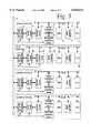
- FIG. 1is a block diagram of a computer implementing the preferred embodiment of the invention showing the major components and their interconnection.
- FIG. 2is a more detailed diagram of a section of FIG. 1 showing an example of the data transfer process.
- FIG. 3is a block diagram of a computer network implementing an alternate embodiment of the invention.
- the present inventionaddresses the problem of increasing the availability of the cache memory to requests for data by dividing the cache memory into a "master" cache memory 10 and a "slave" cache memory 11.
- Datais transferred from a mass-storage device 12, 13, 14, or 15 to slave cache memory 11 and then from slave cache memory 11 to the master cache memory 10.
- the time required to write data to master cache memory 10is governed by the time required to read that same data from slave cache memory 11 and not the time required to read that same data from the much slower mass-storage devices 12, 13, 14 and 15.
- the access time required to receive data from the a mass storage deviceis often an order of magnitude or more greater than the time required to receive that same data from the slave cache memory. Therefore, master cache memory 10 spends much less time reading data from the slave cache memory 11 than it would reading data directly from a mass-storage device 12, 13, 14 or 15 and is available far more often for serving requests for data.
- the mass-storage devicescan be any number of devices; the four shown are only intended as an example.
- Typical mass-storage devicesinclude disks, tapes, or drums with information stored in magnetic or optical form. The principles of the invention apply equally regardless of the form of mass storage.
- a request to move data from a mass-storage devices 12, 13, 14 or 15 to main memory 16is initiated by the central processing unit (CPU) 17. It is sent by the CPU 17 or the direct memory access controller (DMA) 18 over bus 19 to mass-storage control logic 20.
- the cache memory control logic 21intercepts the request and checks the master cache memory 10 for the requested data. If the requested data is in the master cache memory it is transferred over bus 19 to main memory 16. If the data is not in the master cache memory 10, the request is passed along to mass-storage control logic 20.
- Mass-storage control logic 20determines which mass-storage device contains the requested data and where on that device the data resides. The requested data is sent from the mass-storage device to slave cache memory 11.
- Slave cache memory 11collects the requested data from the mass-storage device at a slower speed determined by the mass storage device.
- the master cache memory 10then reads the data from the slave cache memory 11 at a much higher speed.
- the requested datais then sent from master cache memory 10 to main memory 16 via bus 19.
- Writing to the a mass-storage deviceis handled in much the same way.
- Datais read from main memory 16 and written to master cache memory 10.
- the master cache memorykeeps the data and reads a copy to the slave cache memory 11.
- the slave cache memory 11in turn reads the data to a selected mass-storage device. If a write request is received for data which is already in the master cache memory it is overwritten in the master cache memory by a copy from the main memory. It is then written to the slave cache memory which in turn writes it to a mass-storage device.
- the mass-storage control logic 20 and the cache memory control logic 21act in concert to control the flow of data.
- the CPU 17 or DMA controller 18request data from a mass-storage device 12, 13, 14, or 15, it sends a request to the mass-storage control logic 20. It has no "knowledge" of the cache memory, nor does it need any knowledge of the cache memory.
- the mass-storage devices 12, 13, 14 and 15respond to requests the same as they would in any non-cache memory system.
- the inventioncan be implemented by adding cache memory control logic 21, mass-storage control logic 20, master cache memory 10, and slave cache memory 11 to any computer. No other logic must be changed to implement the invention. In an open architecture system this can be done by plugging in a circuit board to a pre-existing system, however, a typical system would be a mass-storage controller 27 which would also include the DMA 18.
- the slave cache memory 11is dual-ported static RAM which acts as a speed adjustment buffer.
- Good examples of this kind of RAMare CY7C130, CY7C140, CY7C132, and CY7C140 produced by Cypress Semiconductor of San Jose, Calif.
- the slave cache memory 11is logically organized as a circular queue 20; data is read out in the same order that it is written in.
- a write pointer 21moves through the memory, writing data from either the master cache memory 10 or one of the mass-storage devices 12, 13, 14 and 15.
- a read pointer 22follows the write pointer through the memory reading data to the master cache memory or a mass storage device. Both pointers move at different rates synchronized with the data transfer rate of the mass-storage devices or the data transfer rate of the master cache memory.
- the slave cache memory 11should be at least twice the size of one sector of data from the mass-storage devices.
- a sectoris the smallest unit of data that the a mass-storage can address.
- a sectormust be completely written to the slave cache memory 11 before it can be read out. If the slave cache memory 11 holds the equivalent of two sectors of memory it can write one sector from the a mass-storage device and read one sector to the master cache memory at the same time.
- sector X 23is being read from the slave cache memory 11 at read pointer 22 and written to master cache memory 10 at write pointer 24.
- Sector Y 25is also being read from mass-storage device 14 at read head 26 and written to slave cache memory 11 at write pointer 21.
- a part of sector Z 27remains and is being over written by sector Y 25.
- read pointer 22would be moving at the high speed of master cache memory 12 and write pointer 21 would be moving at the slower speed of mass-storage device 14.
- Cache memoriesare used in several applications in the computer art. The improvements described here are equally applicable to any form of peripheral interface cache memory. Any time there is a significant difference in speed between two forms of stored data, cache memories and the present invention can be beneficial.
- the slave cache memoryneed not be dual-ported static RAM. Dual-ported static RAM provides the best performance, but at a high price. Single-ported RAM would provide slightly less performance at a considerable savings. Time sharing control needs to be added if single-ported RAM is used so both the mass-storage device and master cache memory have equal access to the slave cache memory.
- a series of registerscan also be used for the slave cache memory with much the same effect as the single-ported RAM. Time sharing controls would be needed and it would be slower but less expensive.
- the preferred embodimentalso discloses cache memories as part of the a mass-storage controller.
- the physical layout of the circuitsis not important.
- the cache memoriesmay also be mounted out side the cache memory controller but provide the same function.
- FIG. 3demonstrates how to apply the invention to a network file system.
- Work station 30very closely resembles FIG. 1.
- the mass-storage devicesare replaced with a network interface 31.
- Mass storageis provided in a central file server 33 through a network 34.
- the file serveralso provides mass storage for workstations 35 and 36.
- the inventionwould be applied to work stations 30, 35, and 36 in the same manner so only workstation 30 will be described. This configuration is merely demonstrative; any combination of file servers and work stations would be equally applicable.
- a request to move data from mass-storage device 32 to main memory 16is initiated by the central processing unit (CPU) 17. It is sent by the CPU 17 or the direct memory access controller (DMA) 18 over bus 19 to network control logic 37. However, the cache memory control logic 21 intercepts the request and checks the master cache memory 10 for the requested data. If the requested data is in the master cache memory it is transferred over bus 19 to main memory 16. If the data is not in the master cache memory 10, the request is passed along to network control logic 37. Network control logic 37 in turn requests the data from file server 33 over network 34. The file server CPU 38 receives the request and sends the requested data to network cache memory 39. Under control of the file server network control logic 40, the data is sent through the file server network interface 41, network 34 and network interface 31 to slave cache memory 11.
- DMAdirect memory access controller
- Slave cache memory 11collects the requested data from network interface 31 at a slower speed determined by the network.
- the master cache memory 10then reads the data from the slave cache memory 11 at a much higher speed.
- the requested datais then sent from master cache memory 10 to main memory 16 via bus 19.
- Mass-storage device 32Writing to mass-storage device 32 is handled in much the same way.
- Datais read from main memory 16 and written to master cache memory 10.
- the master cache memorykeeps the data and reads a copy to the slave cache memory 11.
- the slave cache memory 11in turn reads the data to network interface 31 and through the network to mass-storage device 32. If a write request is received for data which is already in the master cache memory it is overwritten in the master cache memory by a copy from the main memory. It is then written to the slave cache memory which in turn sends the data back through the network the mass-storage device 32.
Landscapes
- Engineering & Computer Science (AREA)
- Theoretical Computer Science (AREA)
- Physics & Mathematics (AREA)
- General Engineering & Computer Science (AREA)
- General Physics & Mathematics (AREA)
- Memory System Of A Hierarchy Structure (AREA)
Abstract
Description
Claims (9)
Priority Applications (1)
| Application Number | Priority Date | Filing Date | Title |
|---|---|---|---|
| US08/131,029US6038641A (en) | 1988-12-30 | 1993-10-04 | Two stage cache memory system and method |
Applications Claiming Priority (4)
| Application Number | Priority Date | Filing Date | Title |
|---|---|---|---|
| US29218988A | 1988-12-30 | 1988-12-30 | |
| US65796991A | 1991-02-20 | 1991-02-20 | |
| US91889292A | 1992-07-16 | 1992-07-16 | |
| US08/131,029US6038641A (en) | 1988-12-30 | 1993-10-04 | Two stage cache memory system and method |
Related Parent Applications (1)
| Application Number | Title | Priority Date | Filing Date |
|---|---|---|---|
| US91889292AContinuation | 1988-12-30 | 1992-07-16 |
Publications (1)
| Publication Number | Publication Date |
|---|---|
| US6038641Atrue US6038641A (en) | 2000-03-14 |
Family
ID=27404113
Family Applications (1)
| Application Number | Title | Priority Date | Filing Date |
|---|---|---|---|
| US08/131,029Expired - LifetimeUS6038641A (en) | 1988-12-30 | 1993-10-04 | Two stage cache memory system and method |
Country Status (1)
| Country | Link |
|---|---|
| US (1) | US6038641A (en) |
Cited By (27)
| Publication number | Priority date | Publication date | Assignee | Title |
|---|---|---|---|---|
| US6304924B1 (en)* | 1999-02-02 | 2001-10-16 | International Business Machines Corporation | Two lock-free, constant-space, multiple-(impure)-reader, single-writer structures |
| US20020087789A1 (en)* | 1998-12-30 | 2002-07-04 | Walton John K. | Data storage system |
| GB2366425B (en)* | 2000-03-31 | 2004-11-10 | Emc Corp | Data storage system |
| GB2366424B (en)* | 2000-03-31 | 2004-11-10 | Emc Corp | Data storage system |
| US20050144223A1 (en)* | 2003-10-20 | 2005-06-30 | Rhode Island Board Of Governors For Higher Education | Bottom-up cache structure for storage servers |
| US6981070B1 (en)* | 2000-07-12 | 2005-12-27 | Shun Hang Luk | Network storage device having solid-state non-volatile memory |
| US7003601B1 (en) | 2000-03-31 | 2006-02-21 | Emc Corporation | Data storage system having separate data transfer section and message network with plural directions on a common printed circuit board |
| US7007194B1 (en) | 2000-06-29 | 2006-02-28 | Emc Corporation | Data storage system having point-to-point configuration |
| US7043603B2 (en) | 2003-10-07 | 2006-05-09 | Hitachi, Ltd. | Storage device control unit and method of controlling the same |
| US20060136779A1 (en)* | 2004-12-20 | 2006-06-22 | Lee Sang-Min | Object-based storage device with low process load and control method thereof |
| US7117275B1 (en) | 1999-01-04 | 2006-10-03 | Emc Corporation | Data storage system having separate data transfer section and message network |
| US20070124476A1 (en)* | 2003-06-27 | 2007-05-31 | Oesterreicher Richard T | System and method for digital media server load balancing |
| US20100234857A1 (en)* | 1998-11-20 | 2010-09-16 | Intuitve Surgical Operations, Inc. | Medical robotic system with operatively couplable simulator unit for surgeon training |
| US20100299553A1 (en)* | 2009-05-25 | 2010-11-25 | Alibaba Group Holding Limited | Cache data processing using cache cluster with configurable modes |
| US7865266B2 (en) | 1998-11-20 | 2011-01-04 | Intuitive Surgical Operations, Inc. | Cooperative minimally invasive telesurgical system |
| US20140310465A1 (en)* | 2013-04-16 | 2014-10-16 | International Business Machines Corporation | Backup cache with immediate availability |
| US8870900B2 (en) | 1999-11-09 | 2014-10-28 | Intuitive Surgical Operations, Inc. | Endoscopic beating-heart stabilizer and vessel occlusion fastener |
| US9039681B2 (en) | 2002-01-16 | 2015-05-26 | Intuitive Surgical Operations, Inc. | Minimally invasive surgical training using robotics and telecollaboration |
| US9119654B2 (en) | 1998-11-20 | 2015-09-01 | Intuitive Surgical Operations, Inc. | Stabilizer for robotic beating-heart surgery |
| US9271798B2 (en) | 1998-11-20 | 2016-03-01 | Intuitive Surgical Operations, Inc. | Multi-user medical robotic system for collaboration or training in minimally invasive surgical procedures |
| US9298617B2 (en) | 2013-04-16 | 2016-03-29 | International Business Machines Corporation | Parallel destaging with replicated cache pinning |
| US9298398B2 (en) | 2013-04-16 | 2016-03-29 | International Business Machines Corporation | Fine-grained control of data placement |
| US9329938B2 (en) | 2013-04-16 | 2016-05-03 | International Business Machines Corporation | Essential metadata replication |
| US9417964B2 (en) | 2013-04-16 | 2016-08-16 | International Business Machines Corporation | Destaging cache data using a distributed freezer |
| US9423981B2 (en) | 2013-04-16 | 2016-08-23 | International Business Machines Corporation | Logical region allocation with immediate availability |
| US9575675B2 (en) | 2013-04-16 | 2017-02-21 | International Business Machines Corporation | Managing metadata and data for a logical volume in a distributed and declustered system |
| US10671396B2 (en)* | 2016-06-14 | 2020-06-02 | Robert Bosch Gmbh | Method for operating a processing unit |
Citations (14)
| Publication number | Priority date | Publication date | Assignee | Title |
|---|---|---|---|---|
| US4020466A (en)* | 1974-07-05 | 1977-04-26 | Ibm Corporation | Memory hierarchy system with journaling and copy back |
| US4032899A (en)* | 1975-05-05 | 1977-06-28 | International Business Machines Corporation | Apparatus and method for switching of data |
| US4048625A (en)* | 1976-05-05 | 1977-09-13 | General Electric Company | Buffered print control system using fifo memory |
| US4181937A (en)* | 1976-11-10 | 1980-01-01 | Fujitsu Limited | Data processing system having an intermediate buffer memory |
| US4268907A (en)* | 1979-01-22 | 1981-05-19 | Honeywell Information Systems Inc. | Cache unit bypass apparatus |
| US4298929A (en)* | 1979-01-26 | 1981-11-03 | International Business Machines Corporation | Integrated multilevel storage hierarchy for a data processing system with improved channel to memory write capability |
| US4409656A (en)* | 1980-03-13 | 1983-10-11 | Her Majesty The Queen, In Right Of Canada As Represented By The Minister Of National Defense | Serial data bus communication system |
| US4464712A (en)* | 1981-07-06 | 1984-08-07 | International Business Machines Corporation | Second level cache replacement method and apparatus |
| US4476526A (en)* | 1981-11-27 | 1984-10-09 | Storage Technology Corporation | Cache buffered memory subsystem |
| US4551799A (en)* | 1983-02-28 | 1985-11-05 | Honeywell Information Systems Inc. | Verification of real page numbers of stack stored prefetched instructions from instruction cache |
| US4780808A (en)* | 1981-11-27 | 1988-10-25 | Storage Technology Corporation | Control of cache buffer for memory subsystem |
| US4833601A (en)* | 1987-05-28 | 1989-05-23 | Bull Hn Information Systems Inc. | Cache resiliency in processing a variety of address faults |
| US4858111A (en)* | 1983-07-29 | 1989-08-15 | Hewlett-Packard Company | Write-back cache system using concurrent address transfers to setup requested address in main memory before dirty miss signal from cache |
| US4872111A (en)* | 1986-08-27 | 1989-10-03 | Amdahl Corporation | Monolithic semi-custom IC having standard LSI sections and coupling gate array sections |
- 1993
- 1993-10-04USUS08/131,029patent/US6038641A/ennot_activeExpired - Lifetime
Patent Citations (14)
| Publication number | Priority date | Publication date | Assignee | Title |
|---|---|---|---|---|
| US4020466A (en)* | 1974-07-05 | 1977-04-26 | Ibm Corporation | Memory hierarchy system with journaling and copy back |
| US4032899A (en)* | 1975-05-05 | 1977-06-28 | International Business Machines Corporation | Apparatus and method for switching of data |
| US4048625A (en)* | 1976-05-05 | 1977-09-13 | General Electric Company | Buffered print control system using fifo memory |
| US4181937A (en)* | 1976-11-10 | 1980-01-01 | Fujitsu Limited | Data processing system having an intermediate buffer memory |
| US4268907A (en)* | 1979-01-22 | 1981-05-19 | Honeywell Information Systems Inc. | Cache unit bypass apparatus |
| US4298929A (en)* | 1979-01-26 | 1981-11-03 | International Business Machines Corporation | Integrated multilevel storage hierarchy for a data processing system with improved channel to memory write capability |
| US4409656A (en)* | 1980-03-13 | 1983-10-11 | Her Majesty The Queen, In Right Of Canada As Represented By The Minister Of National Defense | Serial data bus communication system |
| US4464712A (en)* | 1981-07-06 | 1984-08-07 | International Business Machines Corporation | Second level cache replacement method and apparatus |
| US4476526A (en)* | 1981-11-27 | 1984-10-09 | Storage Technology Corporation | Cache buffered memory subsystem |
| US4780808A (en)* | 1981-11-27 | 1988-10-25 | Storage Technology Corporation | Control of cache buffer for memory subsystem |
| US4551799A (en)* | 1983-02-28 | 1985-11-05 | Honeywell Information Systems Inc. | Verification of real page numbers of stack stored prefetched instructions from instruction cache |
| US4858111A (en)* | 1983-07-29 | 1989-08-15 | Hewlett-Packard Company | Write-back cache system using concurrent address transfers to setup requested address in main memory before dirty miss signal from cache |
| US4872111A (en)* | 1986-08-27 | 1989-10-03 | Amdahl Corporation | Monolithic semi-custom IC having standard LSI sections and coupling gate array sections |
| US4833601A (en)* | 1987-05-28 | 1989-05-23 | Bull Hn Information Systems Inc. | Cache resiliency in processing a variety of address faults |
Cited By (52)
| Publication number | Priority date | Publication date | Assignee | Title |
|---|---|---|---|---|
| US9271798B2 (en) | 1998-11-20 | 2016-03-01 | Intuitive Surgical Operations, Inc. | Multi-user medical robotic system for collaboration or training in minimally invasive surgical procedures |
| US8600551B2 (en) | 1998-11-20 | 2013-12-03 | Intuitive Surgical Operations, Inc. | Medical robotic system with operatively couplable simulator unit for surgeon training |
| US20100234857A1 (en)* | 1998-11-20 | 2010-09-16 | Intuitve Surgical Operations, Inc. | Medical robotic system with operatively couplable simulator unit for surgeon training |
| US8914150B2 (en) | 1998-11-20 | 2014-12-16 | Intuitive Surgical Operations, Inc. | Cooperative minimally invasive telesurgical system |
| US9119654B2 (en) | 1998-11-20 | 2015-09-01 | Intuitive Surgical Operations, Inc. | Stabilizer for robotic beating-heart surgery |
| US9867671B2 (en) | 1998-11-20 | 2018-01-16 | Intuitive Surgical Operations, Inc. | Multi-user medical robotic system for collaboration or training in minimally invasive surgical procedures |
| US9636186B2 (en) | 1998-11-20 | 2017-05-02 | Intuitive Surgical Operations, Inc. | Multi-user medical robotic system for collaboration or training in minimally invasive surgical procedures |
| US8666544B2 (en) | 1998-11-20 | 2014-03-04 | Intuitive Surgical Operations, Inc. | Cooperative minimally invasive telesurgical system |
| US7865266B2 (en) | 1998-11-20 | 2011-01-04 | Intuitive Surgical Operations, Inc. | Cooperative minimally invasive telesurgical system |
| US8504201B2 (en) | 1998-11-20 | 2013-08-06 | Intuitive Sugrical Operations, Inc. | Cooperative minimally invasive telesurgical system |
| US20110137322A1 (en)* | 1998-11-20 | 2011-06-09 | Intuitive Surgical Operations | Cooperative Minimally Invasive Telesurgical System |
| US8489235B2 (en) | 1998-11-20 | 2013-07-16 | Intuitive Surgical Operations, Inc. | Cooperative minimally invasive telesurgical system |
| US9666101B2 (en) | 1998-11-20 | 2017-05-30 | Intuitive Surgical Operations, Inc. | Multi-user medical robotic system for collaboration or training in minimally invasive surgical procedures |
| US6988152B2 (en) | 1998-12-30 | 2006-01-17 | Emc Corporation | Data storage system |
| US20020087789A1 (en)* | 1998-12-30 | 2002-07-04 | Walton John K. | Data storage system |
| US6957285B2 (en) | 1998-12-30 | 2005-10-18 | Emc Corporation | Data storage system |
| US20020156976A1 (en)* | 1998-12-30 | 2002-10-24 | Walton John K. | Data storage system |
| US7117275B1 (en) | 1999-01-04 | 2006-10-03 | Emc Corporation | Data storage system having separate data transfer section and message network |
| US6304924B1 (en)* | 1999-02-02 | 2001-10-16 | International Business Machines Corporation | Two lock-free, constant-space, multiple-(impure)-reader, single-writer structures |
| US8870900B2 (en) | 1999-11-09 | 2014-10-28 | Intuitive Surgical Operations, Inc. | Endoscopic beating-heart stabilizer and vessel occlusion fastener |
| US7010575B1 (en) | 2000-03-31 | 2006-03-07 | Emc Corporation | Data storage system having separate data transfer section and message network having bus arbitration |
| US7003601B1 (en) | 2000-03-31 | 2006-02-21 | Emc Corporation | Data storage system having separate data transfer section and message network with plural directions on a common printed circuit board |
| GB2366424B (en)* | 2000-03-31 | 2004-11-10 | Emc Corp | Data storage system |
| GB2366425B (en)* | 2000-03-31 | 2004-11-10 | Emc Corp | Data storage system |
| US7007194B1 (en) | 2000-06-29 | 2006-02-28 | Emc Corporation | Data storage system having point-to-point configuration |
| US6981070B1 (en)* | 2000-07-12 | 2005-12-27 | Shun Hang Luk | Network storage device having solid-state non-volatile memory |
| US9039681B2 (en) | 2002-01-16 | 2015-05-26 | Intuitive Surgical Operations, Inc. | Minimally invasive surgical training using robotics and telecollaboration |
| US9786203B2 (en) | 2002-01-16 | 2017-10-10 | Intuitive Surgical Operations, Inc. | Minimally invasive surgical training using robotics and telecollaboration |
| US7680938B2 (en)* | 2003-06-27 | 2010-03-16 | Oesterreicher Richard T | Video on demand digital server load balancing |
| US20070124476A1 (en)* | 2003-06-27 | 2007-05-31 | Oesterreicher Richard T | System and method for digital media server load balancing |
| US7043603B2 (en) | 2003-10-07 | 2006-05-09 | Hitachi, Ltd. | Storage device control unit and method of controlling the same |
| US20050144223A1 (en)* | 2003-10-20 | 2005-06-30 | Rhode Island Board Of Governors For Higher Education | Bottom-up cache structure for storage servers |
| US20060136779A1 (en)* | 2004-12-20 | 2006-06-22 | Lee Sang-Min | Object-based storage device with low process load and control method thereof |
| US7707337B2 (en)* | 2004-12-20 | 2010-04-27 | Electronics And Telecommunications Research Institute | Object-based storage device with low process load and control method thereof |
| US20100299553A1 (en)* | 2009-05-25 | 2010-11-25 | Alibaba Group Holding Limited | Cache data processing using cache cluster with configurable modes |
| US20150169421A1 (en)* | 2009-05-25 | 2015-06-18 | Alibaba Group Holding Limited | Cache data processing using cache cluster with configurable modes |
| JP2012528382A (en)* | 2009-05-25 | 2012-11-12 | アリババ・グループ・ホールディング・リミテッド | Cache data processing using cache clusters in configurable mode |
| US8972773B2 (en)* | 2009-05-25 | 2015-03-03 | Alibaba Group Holding Limited | Cache data processing using cache cluster with configurable modes |
| US9317384B2 (en)* | 2009-05-25 | 2016-04-19 | Alibaba Group Holding Limited | Cache data processing using cache cluster with configurable modes |
| US9298398B2 (en) | 2013-04-16 | 2016-03-29 | International Business Machines Corporation | Fine-grained control of data placement |
| US9423981B2 (en) | 2013-04-16 | 2016-08-23 | International Business Machines Corporation | Logical region allocation with immediate availability |
| US9535840B2 (en) | 2013-04-16 | 2017-01-03 | International Business Machines Corporation | Parallel destaging with replicated cache pinning |
| US9547446B2 (en) | 2013-04-16 | 2017-01-17 | International Business Machines Corporation | Fine-grained control of data placement |
| US9575675B2 (en) | 2013-04-16 | 2017-02-21 | International Business Machines Corporation | Managing metadata and data for a logical volume in a distributed and declustered system |
| US9600192B2 (en) | 2013-04-16 | 2017-03-21 | International Business Machines Corporation | Managing metadata and data for a logical volume in a distributed and declustered system |
| US9619404B2 (en)* | 2013-04-16 | 2017-04-11 | International Business Machines Corporation | Backup cache with immediate availability |
| US9417964B2 (en) | 2013-04-16 | 2016-08-16 | International Business Machines Corporation | Destaging cache data using a distributed freezer |
| US9329938B2 (en) | 2013-04-16 | 2016-05-03 | International Business Machines Corporation | Essential metadata replication |
| US9740416B2 (en) | 2013-04-16 | 2017-08-22 | International Business Machines Corporation | Essential metadata replication |
| US9298617B2 (en) | 2013-04-16 | 2016-03-29 | International Business Machines Corporation | Parallel destaging with replicated cache pinning |
| US20140310465A1 (en)* | 2013-04-16 | 2014-10-16 | International Business Machines Corporation | Backup cache with immediate availability |
| US10671396B2 (en)* | 2016-06-14 | 2020-06-02 | Robert Bosch Gmbh | Method for operating a processing unit |
Similar Documents
| Publication | Publication Date | Title |
|---|---|---|
| US6038641A (en) | Two stage cache memory system and method | |
| US4476526A (en) | Cache buffered memory subsystem | |
| US6467022B1 (en) | Extending adapter memory with solid state disks in JBOD and RAID environments | |
| US5146578A (en) | Method of varying the amount of data prefetched to a cache memory in dependence on the history of data requests | |
| US5224217A (en) | Computer system which uses a least-recently-used algorithm for manipulating data tags when performing cache replacement | |
| US5649230A (en) | System for transferring data using value in hardware FIFO'S unused data start pointer to update virtual FIFO'S start address pointer for fast context switching | |
| US6493773B1 (en) | Data validity measure for efficient implementation of first-in-first-out memories for multi-processor systems | |
| US6012106A (en) | Prefetch management for DMA read transactions depending upon past history of actual transfer lengths | |
| US8195918B2 (en) | Memory hub with internal cache and/or memory access prediction | |
| US8607005B2 (en) | Monitoring program execution to learn data blocks accessed by software process for facilitating efficient prefetching | |
| US6578102B1 (en) | Tracking and control of prefetch data in a PCI bus system | |
| US7337281B2 (en) | Storage system and data caching method in the system | |
| US5265236A (en) | Method and apparatus for increasing the speed of memory access in a virtual memory system having fast page mode | |
| US5890012A (en) | System for programming peripheral with address and direction information and sending the information through data bus or control line when DMA controller asserts data knowledge line | |
| CN1337718A (en) | Storage controlling technology | |
| US12026397B2 (en) | Hybrid memory module having a volatile memory subsystem and a module controller configurable to provide data to accompany externally sourced data strobes to the volatile memory subsystem | |
| US7895397B2 (en) | Using inter-arrival times of data requests to cache data in a computing environment | |
| JPH0422016B2 (en) | ||
| US5588128A (en) | Dynamic direction look ahead read buffer | |
| US5974497A (en) | Computer with cache-line buffers for storing prefetched data for a misaligned memory access | |
| US6799228B2 (en) | Input/output control apparatus, input/output control method and information storage system | |
| US20010047439A1 (en) | Efficient implementation of first-in-first-out memories for multi-processor systems | |
| US6134632A (en) | Controller that supports data merging utilizing a slice addressable memory array | |
| EP0745941A2 (en) | A system and method for providing a flexible memory hierarchy | |
| US6877060B2 (en) | Dynamic delayed transaction buffer configuration based on bus frequency |
Legal Events
| Date | Code | Title | Description |
|---|---|---|---|
| AS | Assignment | Owner name:PACKARD BELL NEC, CALIFORNIA Free format text:ASSIGNMENT OF ASSIGNORS INTEREST;ASSIGNOR:ZENITH DATA SYSTEMS CORPORATION;REEL/FRAME:009075/0073 Effective date:19970320 | |
| STCF | Information on status: patent grant | Free format text:PATENTED CASE | |
| AS | Assignment | Owner name:NEC CORPORATION, JAPAN Free format text:ASSIGNMENT OF ASSIGNORS INTEREST;ASSIGNOR:PACKARD BELL NEC, INC.;REEL/FRAME:011007/0153 Effective date:20000223 | |
| FPAY | Fee payment | Year of fee payment:4 | |
| FPAY | Fee payment | Year of fee payment:8 | |
| AS | Assignment | Owner name:ZENITH DATA SYSTEMS CORPORATION, ILLINOIS Free format text:ASSIGNMENT OF ASSIGNORS INTEREST;ASSIGNOR:ZANGENEHPOUR, SAIED;REEL/FRAME:022645/0872 Effective date:19881229 | |
| AS | Assignment | Owner name:ZENITH ELECTRONICS CORPORATION, ILLINOIS Free format text:ASSIGNMENT OF ASSIGNORS INTEREST;ASSIGNOR:ZANGENEHPOUR, SAIED;REEL/FRAME:022742/0905 Effective date:19881229 | |
| AS | Assignment | Owner name:ZENITH DATA SYSTEMS CORPORATION, MICHIGAN Free format text:ASSIGNMENT OF ASSIGNORS INTEREST;ASSIGNOR:ZENITH ELECTRONICS CORPORATION;REEL/FRAME:022746/0581 Effective date:19891228 | |
| AS | Assignment | Owner name:CRESCENT MOON, LLC, CALIFORNIA Free format text:ASSIGNMENT OF ASSIGNORS INTEREST;ASSIGNOR:NEC CORPORATION;REEL/FRAME:022973/0287 Effective date:20090616 | |
| FPAY | Fee payment | Year of fee payment:12 | |
| AS | Assignment | Owner name:RPX CORPORATION, CALIFORNIA Free format text:ASSIGNMENT OF ASSIGNORS INTEREST;ASSIGNOR:OAR ISLAND LLC;REEL/FRAME:028146/0023 Effective date:20120420 |