US6037648A - Semiconductor structure including a conductive fuse and process for fabrication thereof - Google Patents
Semiconductor structure including a conductive fuse and process for fabrication thereofDownload PDFInfo
- Publication number
- US6037648A US6037648AUS09/105,647US10564798AUS6037648AUS 6037648 AUS6037648 AUS 6037648AUS 10564798 AUS10564798 AUS 10564798AUS 6037648 AUS6037648 AUS 6037648A
- Authority
- US
- United States
- Prior art keywords
- layer
- semiconductor structure
- conductive
- etch stop
- fuse
- Prior art date
- Legal status (The legal status is an assumption and is not a legal conclusion. Google has not performed a legal analysis and makes no representation as to the accuracy of the status listed.)
- Expired - Lifetime
Links
Images


Classifications
- E—FIXED CONSTRUCTIONS
- E01—CONSTRUCTION OF ROADS, RAILWAYS, OR BRIDGES
- E01F—ADDITIONAL WORK, SUCH AS EQUIPPING ROADS OR THE CONSTRUCTION OF PLATFORMS, HELICOPTER LANDING STAGES, SIGNS, SNOW FENCES, OR THE LIKE
- E01F9/00—Arrangement of road signs or traffic signals; Arrangements for enforcing caution
- H—ELECTRICITY
- H01—ELECTRIC ELEMENTS
- H01L—SEMICONDUCTOR DEVICES NOT COVERED BY CLASS H10
- H01L21/00—Processes or apparatus adapted for the manufacture or treatment of semiconductor or solid state devices or of parts thereof
- H01L21/70—Manufacture or treatment of devices consisting of a plurality of solid state components formed in or on a common substrate or of parts thereof; Manufacture of integrated circuit devices or of parts thereof
- H01L21/71—Manufacture of specific parts of devices defined in group H01L21/70
- H01L21/768—Applying interconnections to be used for carrying current between separate components within a device comprising conductors and dielectrics
- H01L21/76838—Applying interconnections to be used for carrying current between separate components within a device comprising conductors and dielectrics characterised by the formation and the after-treatment of the conductors
- H01L21/76885—By forming conductive members before deposition of protective insulating material, e.g. pillars, studs
- E—FIXED CONSTRUCTIONS
- E01—CONSTRUCTION OF ROADS, RAILWAYS, OR BRIDGES
- E01H—STREET CLEANING; CLEANING OF PERMANENT WAYS; CLEANING BEACHES; DISPERSING OR PREVENTING FOG IN GENERAL CLEANING STREET OR RAILWAY FURNITURE OR TUNNEL WALLS
- E01H1/00—Removing undesirable matter from roads or like surfaces, with or without moistening of the surface
- E01H1/02—Brushing apparatus, e.g. with auxiliary instruments for mechanically loosening dirt
- H—ELECTRICITY
- H01—ELECTRIC ELEMENTS
- H01L—SEMICONDUCTOR DEVICES NOT COVERED BY CLASS H10
- H01L23/00—Details of semiconductor or other solid state devices
- H01L23/52—Arrangements for conducting electric current within the device in operation from one component to another, i.e. interconnections, e.g. wires, lead frames
- H01L23/522—Arrangements for conducting electric current within the device in operation from one component to another, i.e. interconnections, e.g. wires, lead frames including external interconnections consisting of a multilayer structure of conductive and insulating layers inseparably formed on the semiconductor body
- H01L23/525—Arrangements for conducting electric current within the device in operation from one component to another, i.e. interconnections, e.g. wires, lead frames including external interconnections consisting of a multilayer structure of conductive and insulating layers inseparably formed on the semiconductor body with adaptable interconnections
- H01L23/5256—Arrangements for conducting electric current within the device in operation from one component to another, i.e. interconnections, e.g. wires, lead frames including external interconnections consisting of a multilayer structure of conductive and insulating layers inseparably formed on the semiconductor body with adaptable interconnections comprising fuses, i.e. connections having their state changed from conductive to non-conductive
- H—ELECTRICITY
- H01—ELECTRIC ELEMENTS
- H01L—SEMICONDUCTOR DEVICES NOT COVERED BY CLASS H10
- H01L2924/00—Indexing scheme for arrangements or methods for connecting or disconnecting semiconductor or solid-state bodies as covered by H01L24/00
- H01L2924/0001—Technical content checked by a classifier
- H01L2924/0002—Not covered by any one of groups H01L24/00, H01L24/00 and H01L2224/00
Definitions
- the present inventionis concerned with a semiconductor structure that includes a conductive fuse, and more particularly relates to providing a conductive fuse having a self-aligned isolation cap thereon.
- the present inventionrelates to a fabrication process for achieving the desired structure.
- the fabrication process of the present inventionmakes it possible to provide a well controlled relatively thin dielectric layer over the fuse which is self-aligned to the fuse.
- DRAMdynamic random access memory
- SRAMstatic random access memory
- fusesSuch can provide for redundancy for the purpose of preventing reduction of yield of the semiconductor devices which may be caused by random defects generated in the manufacturing process.
- the redundant circuit portionis provided as a spare circuit portion having the same function as a specific circuit portion so that the specific circuit portion which has a defect caused during manufacturing may be replaced with the redundant circuit in order to maintain the function of the entire semiconductor.
- fuse linksprovide for voltage options, packaging pin out options, or any other option desired by the manufacturer to be employed prior to the final processing. This helps increase yield and makes it easier to use one basic design for several different end products.
- the thickness of the insulating layer over the fusetends to have very large variation.
- the large variation in the final insulation thicknessis due to variations in the deposition of isolation between a first and a second conductive level, variations in deposition of the next-to-last insulation layers, non-uniformities during chemical-mechanical polishing and variations in the reactive ion etching to achieve the final thickness.
- the thickness variationoccurs because of the cumulative variations of each of the process steps even when each individual step can be reasonably controlled.
- the variation in thicknesslimits the fuse pitch to that which corresponds to the largest isolation layer generated by the processing.
- the present inventionrelates to improving the control of the thickness of the insulating layer above a fuse structure. Moreover, the present invention makes possible a fuse structure having a relatively thin self-aligned dielectric layer.
- the inventionis concerned with a semiconductor structure comprising a semiconductor substrate, an electrically conductive level on the substrate and a fuse located at this conductive level.
- the fusecomprises a self-aligned dielectric etch stop layer thereon.
- An insulation structureis provided located above the conductive level, but not above the fuse. Electrical connection is provided through the insulation structure to selected locations of the conductive level. A further insulation structure is provided above the electrical connection.
- the inventionencompasses a process for fabricating the above disclosed semiconductor structure. More particularly, the process of the invention comprises providing a semiconductor substrate having a conductive level thereon. A layer of a first dielectric etch stop material is blanket deposited. The layer of the dielectric etch stop material and the conductive level are patterned, preferably by reactive ion etching, thereby creating structures including (i) a fuse structure capped with self-aligned dielectric etch stop material thereon and (ii) conductive lines, and gaps between the structures.
- the process of the inventionis preferably continued by depositing a second dielectric material, different from the etch stop material, over the structures and in the gaps.
- a third dielectric materialis deposited over the second dielectric material.
- the third dielectric material, second dielectric material and first dielectric materialare patterned, preferably by reactive ion etching, to create vias through the third dielectric material, second dielectric material and first dielectric material, thereby exposing selected portions of the conductive level.
- the viasare filled with electrically conductive material to provide electrical interconnection to the selected portions of the conductive level.
- a further insulating layeris provided over the entire structure, and then via is created through the insulating structure down to the etch stop layer on the fuse.
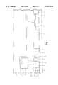
- FIGS. 1-5illustrate the semiconductor structure of the present invention during various stages of preparation.
- the semiconductor structure of the inventionpreferably comprises a semiconductor substrate 10; an electrically conductive material at a level 1 on the substrate; a conductive fuse 21 located at the conductive level 1 wherein the fuse comprises a conductive segment of the level 1 conductive material with self-aligned dielectric etch stop layer 2 thereon; insulation structure 3 (optionally including additional insulating layer 13) located above the conductive level 1 and in between conductive lines 22 of the conductive level 1, but not above the fuse 21; and electrical interconnection 4 through the insulation structure 3 (and 13 if present) to selected locations of the conductive level 1.
- the structure of the inventionpreferably further comprises a further insulating structure shown as layers 5-7 over the electrical interconnection 4.
- a semiconductor substrate structure 10is provided with an electrically conductive layer 1 (also referred to as level 1).
- the conductive layer 1is preferably formed from a conductive material selected from the group consisting of aluminum, copper, aluminum copper alloys, and doped polysilicon having metallic-type conductivity.
- the electrically conductive level 1may be a wiring level or gate conductor level and may be formed by any technique normally used to form those conductive levels.
- Layer 1is preferably about 50 to 1000 nanometers thick, more preferably about 200 to 500 nanometers thick.
- a layer 2 of a dielectric etch stop materialis blanket deposited on top of layer 1.
- the layer 2is preferably a silicon nitride and/or silicon oxynitride.
- the silicon nitride and/or silicon oxynitridecan be provided by chemical vapor deposition (CVD) or other known technique.
- the maximum thickness of layer 2is preferably about 450 nanometers.
- Layer 2is more preferably about 25 to 200 nanometers thick, more preferably about 50 to 100 nanometers thick, a typical example being about 50 nanometers.
- a silicon dioxide layer(not shown) can also be present as a component of layer 2 above the silicon nitride and/or silicon oxynitride layer.
- the dielectric etch stop material layer 2 and the conductive layer 1are patterned, preferably by reactive ion etching (RIE).
- RIEreactive ion etching
- the substrateis electrically biased in a chamber that has a plasma of gases made up of a reactive component (e.g. fluorinated hydrocarbon) and an inert gas.
- a reactive componente.g. fluorinated hydrocarbon
- the plasmareacts with the layers to produce volatile reaction products that get pumped away from the chamber.
- wet chemical etchingmay be used as an alternative to reactive ion etching.
- the etching conditionsmay be altered to conditions more suitable for reactive ion etching of metals where the patterned etch stop material acts as a hard mask patterning the conductive features.
- the patterning stepresults in the creation of one or more fuses 21 capped with self-aligned dielectric etch stop material.
- the patterningalso typically results in the formation of other conductive features such as conductive lines 22 and gaps 20 located between the conductive lines 22.
- the fuses 21 capped by the self-aligned dielectric materialare formed prior to providing the next level dielectric material and while there is essentially no material between the conductive lines 21.
- a second dielectric material 3different from the etch stop material, is deposited in the gaps 20 and over the remaining dielectric etch stop material.
- the second dielectric material 3is a relatively dense silicon dioxide material provided by using high density plasma enhanced chemical vapor deposition or other technique.
- the thickness of layer 3 above layer 2is about 40 to 400 nanometers, more preferably about 50 to 200 nanometers.
- a third dielectric layer 13such as silicon oxide from chemical vapor deposition of tetraethylorthosilicate (TEOS) or a silane may be provided.
- TEOStetraethylorthosilicate
- layer 13is about 50 to 1000 nanometers thick, and more preferably about 200 to 400 nanometers thick. In some instances, it may be possible to omit the deposition of silane-derived or TEOS derived silicon oxide if oxide layer 3 is of sufficient thickness.
- the uppermost dielectric layer 3(or 13 if present) is then preferably planarized using chemical mechanical polishing or other appropriate technique.
- the combined thickness of layers 2, 3 and 13is preferably about 350 to 1200 nanometers.
- the dielectric layers 3 and 13are then patterned to provide vias 14 to selected conductive lines 22 and/or other features remaining from conductive layer 1. This patterning can be carried out by reactive ion etching or other suitable technique. A resulting structure is shown in FIG. 3.
- a conductive materialsuch as aluminum, tungsten, titanium, tantalum, or heavily doped polysilicon, is then provided in the vias to provide electrical connection to the underlying conductive feature (e.g. a line 22).
- a portion of conductive materialis also provided above the isolation layer 13 and is patterned, using reactive ion etching or other known technique, thereby resulting in the electrical interconnection structure 4.
- a dielectric layer 5such as silicon dioxide obtained from depositing TEOS.
- This layer 5is preferably about 100 to 1000 nanometers thick and more preferably about 200 to 600 nanometers thick.
- Another layer 6 of silicon nitridemay then be provided by chemical vapor deposition above the TEOS-derived layer 5.
- This layer 6is preferably about 100 to 1000 nanometers thick, more preferably about 200 to 600 nanometers thick.
- a layer 7 of, for example, photosensitive polyimideis then deposited over layer 6.
- Layer 7may be deposited by spraying or spin coating and is preferably about 2 to 10 micrometers thick.
- layer 7is patterned by known lithographic techniques and acts as an etch mask for selectively etching the various dielectric layers above the fuse 21 dielectric etch stop. More particularly, the selective etching is preferably achieved by reactive ion etching.
- nitride layer 6 and oxide layer 5may be etched using a fluorinated hydrocarbon (e.g., C 4 F 8 ) at about 5 to 15 sccm (typically about 8 sccm) and an inert gas (e.g., argon) at about 50 to 100 sccm (typically about 100 sccm).
- a fluorinated hydrocarbone.g., C 4 F 8
- an inert gase.g., argon
- the flow rate of the fluorinated hydrocarbon and inert gasmay be adjusted, to about 5 to 15 sccm (typically about 8 sccm) and about 10 to 25 sccm typically about 15 sccm), respectively, in order to etch the underlying silicon oxide layers 3 and 13 while removing at most only very small amounts of underlying nitride-containing etch stop material layer 2 which is the cap for the fuse 21.
- the process of the inventionadvantageously produces fuses having a controlled thickness insulting layer which provides the design and performance advantages mentioned above.
Landscapes
- Engineering & Computer Science (AREA)
- Microelectronics & Electronic Packaging (AREA)
- Physics & Mathematics (AREA)
- Condensed Matter Physics & Semiconductors (AREA)
- General Physics & Mathematics (AREA)
- Computer Hardware Design (AREA)
- Power Engineering (AREA)
- Civil Engineering (AREA)
- Structural Engineering (AREA)
- Manufacturing & Machinery (AREA)
- Architecture (AREA)
- Design And Manufacture Of Integrated Circuits (AREA)
- Internal Circuitry In Semiconductor Integrated Circuit Devices (AREA)
Abstract
Description
Claims (9)
Priority Applications (6)
| Application Number | Priority Date | Filing Date | Title |
|---|---|---|---|
| US09/105,647US6037648A (en) | 1998-06-26 | 1998-06-26 | Semiconductor structure including a conductive fuse and process for fabrication thereof |
| TW088107991ATW415077B (en) | 1998-06-26 | 1999-05-17 | Semiconductor structure including a conductive fuse and process for fabrication thereof |
| EP99304728AEP0981161B1 (en) | 1998-06-26 | 1999-06-17 | Process of fabricating a semiconductor structure including a conductive fuse |
| DE69939300TDE69939300D1 (en) | 1998-06-26 | 1999-06-17 | Method for producing a semiconductor structure with a conductive fuse |
| JP11174401AJP2000058655A (en) | 1998-06-26 | 1999-06-21 | Semiconductor structure containing conductive fuse and its manufacture |
| KR1019990023659AKR100350545B1 (en) | 1998-06-26 | 1999-06-23 | Semiconductor structure including a conductive fuse and process for fabrication thereof |
Applications Claiming Priority (1)
| Application Number | Priority Date | Filing Date | Title |
|---|---|---|---|
| US09/105,647US6037648A (en) | 1998-06-26 | 1998-06-26 | Semiconductor structure including a conductive fuse and process for fabrication thereof |
Publications (1)
| Publication Number | Publication Date |
|---|---|
| US6037648Atrue US6037648A (en) | 2000-03-14 |
Family
ID=22307017
Family Applications (1)
| Application Number | Title | Priority Date | Filing Date |
|---|---|---|---|
| US09/105,647Expired - LifetimeUS6037648A (en) | 1998-06-26 | 1998-06-26 | Semiconductor structure including a conductive fuse and process for fabrication thereof |
Country Status (6)
| Country | Link |
|---|---|
| US (1) | US6037648A (en) |
| EP (1) | EP0981161B1 (en) |
| JP (1) | JP2000058655A (en) |
| KR (1) | KR100350545B1 (en) |
| DE (1) | DE69939300D1 (en) |
| TW (1) | TW415077B (en) |
Cited By (8)
| Publication number | Priority date | Publication date | Assignee | Title |
|---|---|---|---|---|
| US6180503B1 (en)* | 1999-07-29 | 2001-01-30 | Vanguard International Semiconductor Corporation | Passivation layer etching process for memory arrays with fusible links |
| US6495901B2 (en) | 2001-01-30 | 2002-12-17 | Infineon Technologies Ag | Multi-level fuse structure |
| US6566171B1 (en)* | 2001-06-12 | 2003-05-20 | Lsi Logic Corporation | Fuse construction for integrated circuit structure having low dielectric constant dielectric material |
| US6573125B2 (en)* | 2001-07-04 | 2003-06-03 | Samsung Electronics Co., Ltd. | Method of opening repair fuse of semiconductor device |
| US20040053487A1 (en)* | 2002-09-17 | 2004-03-18 | Taiwan Semiconductor Manufacturing Company | Metal fuse for semiconductor devices |
| US20060289899A1 (en)* | 2005-06-22 | 2006-12-28 | Samsung Electronics Co., Ltd. | Semiconductor devices having fuses and methods of forming the same |
| US20090026575A1 (en)* | 2006-02-07 | 2009-01-29 | Samsung Electronics Co., Ltd. | Semiconductor device and method of manufacturing the same |
| US20090302418A1 (en)* | 2008-06-10 | 2009-12-10 | Samsung Electronics Co., Ltd. | Fuse structure of a semiconductor device |
Families Citing this family (2)
| Publication number | Priority date | Publication date | Assignee | Title |
|---|---|---|---|---|
| US6121074A (en)* | 1998-11-05 | 2000-09-19 | Siemens Aktiengesellschaft | Fuse layout for improved fuse blow process window |
| US20090045484A1 (en) | 2007-08-16 | 2009-02-19 | International Business Machines Corporation | Methods and systems involving electrically reprogrammable fuses |
Citations (6)
| Publication number | Priority date | Publication date | Assignee | Title |
|---|---|---|---|---|
| US5444012A (en)* | 1993-07-20 | 1995-08-22 | Hitachi, Ltd. | Method for manufacturing semiconductor integrated circuit device having a fuse element |
| US5550399A (en)* | 1994-11-03 | 1996-08-27 | Kabushiki Kaisha Toshiba | Integrated circuit with windowed fuse element and contact pad |
| US5578517A (en)* | 1994-10-24 | 1996-11-26 | Taiwan Semiconductor Manufacturing Company Ltd. | Method of forming a highly transparent silicon rich nitride protective layer for a fuse window |
| US5723358A (en)* | 1996-04-29 | 1998-03-03 | Vlsi Technology, Inc. | Method of manufacturing amorphous silicon antifuse structures |
| US5789794A (en)* | 1994-12-29 | 1998-08-04 | Siemens Aktiengesellschaft | Fuse structure for an integrated circuit element |
| US5872390A (en)* | 1995-08-28 | 1999-02-16 | International Business Machines Corporation | Fuse window with controlled fuse oxide thickness |
Family Cites Families (5)
| Publication number | Priority date | Publication date | Assignee | Title |
|---|---|---|---|---|
| JPS59200453A (en)* | 1983-04-27 | 1984-11-13 | Hitachi Ltd | Manufacture of semiconductor device |
| JPS6065545A (en)* | 1983-09-21 | 1985-04-15 | Hitachi Micro Comput Eng Ltd | Manufacturing method of semiconductor device |
| JPS6289338A (en)* | 1985-10-16 | 1987-04-23 | Hitachi Ltd | Semiconductor integrated circuit device and its manufacturing method |
| JPS6480038A (en)* | 1987-09-19 | 1989-03-24 | Hitachi Ltd | Manufacture of semiconductor integrated circuit device |
| US5300456A (en)* | 1993-06-17 | 1994-04-05 | Texas Instruments Incorporated | Metal-to-metal antifuse structure |
- 1998
- 1998-06-26USUS09/105,647patent/US6037648A/ennot_activeExpired - Lifetime
- 1999
- 1999-05-17TWTW088107991Apatent/TW415077B/ennot_activeIP Right Cessation
- 1999-06-17DEDE69939300Tpatent/DE69939300D1/ennot_activeExpired - Lifetime
- 1999-06-17EPEP99304728Apatent/EP0981161B1/ennot_activeExpired - Lifetime
- 1999-06-21JPJP11174401Apatent/JP2000058655A/enactivePending
- 1999-06-23KRKR1019990023659Apatent/KR100350545B1/ennot_activeExpired - Fee Related
Patent Citations (6)
| Publication number | Priority date | Publication date | Assignee | Title |
|---|---|---|---|---|
| US5444012A (en)* | 1993-07-20 | 1995-08-22 | Hitachi, Ltd. | Method for manufacturing semiconductor integrated circuit device having a fuse element |
| US5578517A (en)* | 1994-10-24 | 1996-11-26 | Taiwan Semiconductor Manufacturing Company Ltd. | Method of forming a highly transparent silicon rich nitride protective layer for a fuse window |
| US5550399A (en)* | 1994-11-03 | 1996-08-27 | Kabushiki Kaisha Toshiba | Integrated circuit with windowed fuse element and contact pad |
| US5789794A (en)* | 1994-12-29 | 1998-08-04 | Siemens Aktiengesellschaft | Fuse structure for an integrated circuit element |
| US5872390A (en)* | 1995-08-28 | 1999-02-16 | International Business Machines Corporation | Fuse window with controlled fuse oxide thickness |
| US5723358A (en)* | 1996-04-29 | 1998-03-03 | Vlsi Technology, Inc. | Method of manufacturing amorphous silicon antifuse structures |
Cited By (14)
| Publication number | Priority date | Publication date | Assignee | Title |
|---|---|---|---|---|
| US6180503B1 (en)* | 1999-07-29 | 2001-01-30 | Vanguard International Semiconductor Corporation | Passivation layer etching process for memory arrays with fusible links |
| US6495901B2 (en) | 2001-01-30 | 2002-12-17 | Infineon Technologies Ag | Multi-level fuse structure |
| US6806551B2 (en) | 2001-06-12 | 2004-10-19 | Lsi Logic Corporation | Fuse construction for integrated circuit structure having low dielectric constant dielectric material |
| US6566171B1 (en)* | 2001-06-12 | 2003-05-20 | Lsi Logic Corporation | Fuse construction for integrated circuit structure having low dielectric constant dielectric material |
| US6573125B2 (en)* | 2001-07-04 | 2003-06-03 | Samsung Electronics Co., Ltd. | Method of opening repair fuse of semiconductor device |
| US6753210B2 (en) | 2002-09-17 | 2004-06-22 | Taiwan Semiconductor Manufacturing Company | Metal fuse for semiconductor devices |
| US20040053487A1 (en)* | 2002-09-17 | 2004-03-18 | Taiwan Semiconductor Manufacturing Company | Metal fuse for semiconductor devices |
| US20040219720A1 (en)* | 2002-09-17 | 2004-11-04 | Jeng Shin-Puu | Metal fuse for semiconductor devices |
| US7205588B2 (en) | 2002-09-17 | 2007-04-17 | Taiwan Semiconductor Manufacturing Co., Ltd. | Metal fuse for semiconductor devices |
| US20060289899A1 (en)* | 2005-06-22 | 2006-12-28 | Samsung Electronics Co., Ltd. | Semiconductor devices having fuses and methods of forming the same |
| US7510914B2 (en) | 2005-06-22 | 2009-03-31 | Samsung Electronics Co., Ltd. | Semiconductor devices having fuses and methods of forming the same |
| US20090184391A1 (en)* | 2005-06-22 | 2009-07-23 | Hyun-Chul Yoon | Semiconductor devices having fuses and methods of forming the same |
| US20090026575A1 (en)* | 2006-02-07 | 2009-01-29 | Samsung Electronics Co., Ltd. | Semiconductor device and method of manufacturing the same |
| US20090302418A1 (en)* | 2008-06-10 | 2009-12-10 | Samsung Electronics Co., Ltd. | Fuse structure of a semiconductor device |
Also Published As
| Publication number | Publication date |
|---|---|
| DE69939300D1 (en) | 2008-09-25 |
| EP0981161A2 (en) | 2000-02-23 |
| KR100350545B1 (en) | 2002-08-28 |
| EP0981161B1 (en) | 2008-08-13 |
| KR20000006375A (en) | 2000-01-25 |
| TW415077B (en) | 2000-12-11 |
| EP0981161A3 (en) | 2002-06-12 |
| JP2000058655A (en) | 2000-02-25 |
Similar Documents
| Publication | Publication Date | Title |
|---|---|---|
| US6787911B1 (en) | Interconnect with low dielectric constant insulators for semiconductor integrated circuit manufacturing | |
| US5963827A (en) | Method for producing via contacts in a semiconductor device | |
| US6777346B2 (en) | Planarization using plasma oxidized amorphous silicon | |
| US5918135A (en) | Methods for forming integrated circuit capacitors including dual electrode depositions | |
| US6472317B1 (en) | Dual damascene arrangement for metal interconnection with low k dielectric constant materials in dielectric layers | |
| US20060197231A1 (en) | Backend metallization method and device obtained therefrom | |
| US6806551B2 (en) | Fuse construction for integrated circuit structure having low dielectric constant dielectric material | |
| US6617689B1 (en) | Metal line and method of suppressing void formation therein | |
| KR100277377B1 (en) | Formation method of contact/through hole | |
| US6191031B1 (en) | Process for producing multi-layer wiring structure | |
| US20040147106A1 (en) | Manufacturing of a semiconductor device with a reduced capacitance between wirings | |
| US6037648A (en) | Semiconductor structure including a conductive fuse and process for fabrication thereof | |
| US4786962A (en) | Process for fabricating multilevel metal integrated circuits and structures produced thereby | |
| US6759324B1 (en) | Method of forming a low resistance contact to underlying aluminum interconnect by depositing titanium in a via opening and reacting the titanium with the aluminum | |
| US6893954B2 (en) | Method for patterning a semiconductor wafer | |
| US20070281434A1 (en) | Capacitor of semiconductor device applying damascene process and method of fabricating the same | |
| US20010023990A1 (en) | Semiconductor device and method for fabricating same | |
| US20230178379A1 (en) | Film deposition for patterning process | |
| US6750140B2 (en) | Process for producing contact holes on a metallization structure | |
| US6815222B2 (en) | Method for protecting capacitive elements during production of a semiconductor device | |
| JP4092602B2 (en) | Manufacturing method of semiconductor device | |
| US6352919B1 (en) | Method of fabricating a borderless via | |
| JPH09115875A (en) | Semiconductor device manufacturing method and treatment liquid used in this method | |
| US7417302B2 (en) | Semiconductor device and method of manufacturing the same | |
| KR20040093565A (en) | Method of manufacturing semiconductor device |
Legal Events
| Date | Code | Title | Description |
|---|---|---|---|
| AS | Assignment | Owner name:SIEMENS MICROELECTRONICS, INC., CALIFORNIA Free format text:ASSIGNMENT OF ASSIGNORS INTEREST;ASSIGNORS:SCHNABEL, RAINER F.;SCHUTZ, RONALD J.;TOBBEN, DIRK;REEL/FRAME:009302/0448;SIGNING DATES FROM 19980624 TO 19980625 Owner name:INTERNATIONAL BUSINESS MACHINES CORPORATION, NEW Y Free format text:ASSIGNMENT OF ASSIGNORS INTEREST;ASSIGNORS:ARNDT, KENNETH C.;GAMBINO, JEFFREY P.;MANDELMAN, JACK A.;AND OTHERS;REEL/FRAME:009302/0470;SIGNING DATES FROM 19980616 TO 19980617 | |
| AS | Assignment | Owner name:SIEMENS AKTIENGESELLSCHAFT, GERMANY Free format text:ASSIGNMENT OF ASSIGNORS INTEREST;ASSIGNOR:SIEMENS MICROELECTRONICS, INC.;REEL/FRAME:009895/0603 Effective date:19990316 | |
| STCF | Information on status: patent grant | Free format text:PATENTED CASE | |
| AS | Assignment | Owner name:INFINEON TECHNOLOGIES NORTH AMERICA CORP., CALIFOR Free format text:CHANGE OF NAME;ASSIGNOR:INFINEON TECHNOLOGIES CORPORATION;REEL/FRAME:010996/0994 Effective date:19990929 | |
| CC | Certificate of correction | ||
| FEPP | Fee payment procedure | Free format text:PAYOR NUMBER ASSIGNED (ORIGINAL EVENT CODE: ASPN); ENTITY STATUS OF PATENT OWNER: LARGE ENTITY | |
| FPAY | Fee payment | Year of fee payment:4 | |
| FPAY | Fee payment | Year of fee payment:8 | |
| AS | Assignment | Owner name:INFINEON TECHNOLOGIES AG,GERMANY Free format text:ASSIGNMENT OF ASSIGNORS INTEREST;ASSIGNOR:SIEMENS AKTIENGESELLSCHAFT;REEL/FRAME:024114/0059 Effective date:19990331 | |
| AS | Assignment | Owner name:QIMONDA AG,GERMANY Free format text:ASSIGNMENT OF ASSIGNORS INTEREST;ASSIGNOR:INFINEON TECHNOLOGIES AG;REEL/FRAME:024218/0001 Effective date:20060425 | |
| REMI | Maintenance fee reminder mailed | ||
| FPAY | Fee payment | Year of fee payment:12 | |
| SULP | Surcharge for late payment | Year of fee payment:11 | |
| AS | Assignment | Owner name:INFINEON TECHNOLOGIES AG, GERMANY Free format text:ASSIGNMENT OF ASSIGNORS INTEREST;ASSIGNOR:QIMONDA AG;REEL/FRAME:035623/0001 Effective date:20141009 | |
| AS | Assignment | Owner name:SAMSUNG ELECTRONICS CO., LTD., KOREA, REPUBLIC OF Free format text:ASSIGNMENT OF ASSIGNORS INTEREST;ASSIGNOR:INFINEON TECHNOLOGIES AG;REEL/FRAME:037221/0885 Effective date:20150930 |