US6029252A - Method and apparatus for generating multi-phase clock signals, and circuitry, memory devices, and computer systems using same - Google Patents
Method and apparatus for generating multi-phase clock signals, and circuitry, memory devices, and computer systems using sameDownload PDFInfo
- Publication number
- US6029252A US6029252AUS09/061,859US6185998AUS6029252AUS 6029252 AUS6029252 AUS 6029252AUS 6185998 AUS6185998 AUS 6185998AUS 6029252 AUS6029252 AUS 6029252A
- Authority
- US
- United States
- Prior art keywords
- gate
- output
- coupled
- input
- terminal
- Prior art date
- Legal status (The legal status is an assumption and is not a legal conclusion. Google has not performed a legal analysis and makes no representation as to the accuracy of the status listed.)
- Expired - Lifetime
Links
Images


Classifications
- G—PHYSICS
- G06—COMPUTING OR CALCULATING; COUNTING
- G06F—ELECTRIC DIGITAL DATA PROCESSING
- G06F1/00—Details not covered by groups G06F3/00 - G06F13/00 and G06F21/00
- G06F1/04—Generating or distributing clock signals or signals derived directly therefrom
- G06F1/06—Clock generators producing several clock signals
- G—PHYSICS
- G11—INFORMATION STORAGE
- G11C—STATIC STORES
- G11C7/00—Arrangements for writing information into, or reading information out from, a digital store
- G11C7/22—Read-write [R-W] timing or clocking circuits; Read-write [R-W] control signal generators or management
- H—ELECTRICITY
- H03—ELECTRONIC CIRCUITRY
- H03K—PULSE TECHNIQUE
- H03K5/00—Manipulating of pulses not covered by one of the other main groups of this subclass
- H03K5/15—Arrangements in which pulses are delivered at different times at several outputs, i.e. pulse distributors
- H03K5/15013—Arrangements in which pulses are delivered at different times at several outputs, i.e. pulse distributors with more than two outputs
Definitions
- This inventionrelates to a method and apparatus for generating clock signals having different phases, to circuitry using the clock generating method and apparatus, such as shift register circuits, and to memory devices and computer systems containing the circuitry using the clock generating method and apparatus.
- ROMsread-only memories
- SRAMstatic random access memory
- Processorsgenerally operate at a relatively high speed. Processors such as the Pentium® and Pentium Pro® microprocessors are currently available that operate at clock speeds of at least 200 MHz. However, the remaining components of the computer system, with the exception of SRAM cache, are not capable of operating at the speed of the processor. For this reason, the system memory devices, as well as the input devices, output devices, and data storage devices, are not coupled directly to the processor bus. Instead, the system memory devices are generally coupled to the processor bus through a memory controller, and the input devices, output devices, and data storage devices are coupled to the processor bus through a bus bridge. The memory controller allows the system memory devices to operate at a lower clock frequency that is substantially lower than the clock frequency of the processor.
- the bus bridgeallows the input devices, output devices, and data storage devices to operate at a substantially lower frequency.
- a processor having a 200 MHz clock frequencymay be mounted on a mother board having a 66 MHz clock frequency for controlling the system memory devices and other components.
- Access to system memoryis a frequent operation for the processor.
- much efforthas been devoted to increasing the operating speed of system memory devices.
- DRAMsdynamic random access memories
- SDRAMssynchronous dynamic random access memories
- SDRAMscannot be connected directly to the processor bus, but instead must interface with the processor bus through a memory controller, bus bridge, or similar device.
- the disparity between the operating speed of the processor and the operating speed of SDRAMscontinues to limit the speed at which processors may complete operations requiring access to system memory.
- SyncLinkA solution to this operating speed disparity has been proposed in the form of a computer architecture known as "SyncLink.”
- the system memoryis coupled to the processor either directly through the processor bus or through a memory controller (not shown).
- SyncLink memory devicesreceive command packets that include both control and address information.
- the SyncLink memory devicethen outputs or receives data on a data bus that may be coupled directly to the data bus portion of the processor bus.
- the memory device 16includes a clock divider and delay circuit 40 that receives a master clock signal 42 and generates a large number of other clock and timing signals to control the timing of various operations in the memory device 16.
- the memory device 16also includes a command buffer 46 and an address capture circuit 48 which receive an internal clock CLK signal, a command packet CA0-CA9 on a command bus 50, and a FLAG signal on line 52.
- the command packet CA0-CA9contains control and address information for each memory transfer, and the FLAG signal identifies the start of a command packet which may include more than one 10-bit packet word.
- a command packetis generally in the form of a sequence of 10-bit packet words on the 10-bit command bus 50.
- the command buffer 46receives the command packet from the bus 50, and compares at least a portion of the command packet to identifying data from an ID register 56 to determine if the command packet is directed to the memory device 16 or some other memory device 16 in the event multiple memory devices 16 are used together in a system. If the command buffer determines that the command is directed to the memory device 16, it then provides a command word to a command decoder and sequencer 60. The command decoder and sequencer 60 generates a large number of internal control signals to control the operation of the memory device 16 during a memory transfer.
- the address capture circuit 48also receives the command words from the command bus 50 and outputs a 20-bit address corresponding to the address information in the command.
- the addressis provided to an address sequencer 64 which generates a corresponding 3-bit bank address on bus 66, a 10-bit row address on bus 68, and a 7-bit column address on bus 70.
- the SyncLink memory device 16 shown in FIG. 1largely avoids this problem by using a plurality of memory banks 80, in this case eight memory banks 80a-h. After a memory read from one bank 80a, the bank 80a can be precharged while the remaining banks 80b-h are being accessed. Each of the memory banks 80a-h receive a row address from a respective row latch/decoder/driver 82a-h.
- All of the row latch/decoder/drivers 82a-hreceive the same row address from a predecoder 84 which, in turn, receives a row address from either a row address register 86 or a refresh counter 88 as determined by a multiplexer 90. However, only one of the row latch/decoder/drivers 82a-h is active at any one time as determined by bank control logic 94 as a function of bank data from a bank address register 96.
- the column address on bus 70is applied to a column latch/decoder 100 which, in turn, supplies I/O gating signals to an I/O gating circuit 102.
- the I/O gating circuit 102interfaces with columns of the memory banks 80a-h through sense amplifiers 104. Data is coupled to or from the memory banks 8a-h through the sense amps 104 and I/O gating circuit 102 to a data path subsystem 108 which includes a read data path 110 and a write data path 112.
- the read data path 110includes a read latch 120 receiving and storing data from the I/O gating circuit 102. In the memory device 16 shown in FIG. 1, 64 bits of data are applied to and stored in the read latch 120.
- the read latchthen provides four 16-bit data words to a multiplexer 122.
- the multiplexer 122sequentially applies each of the 16-bit data words to a read FIFO buffer 124. Successive 16-bit data words are clocked through the FIFO buffer 124 by a clock signal generated from an internal clock by a programmable delay circuit 126.
- the FIFO buffer 124sequentially applies the 16-bit words and two clock signals (a clock signal and a quadrature clock signal) to a driver circuit 128 which, in turn, applies the 16-bit data words to a data bus 130 forming part of the processor bus 14.
- the driver circuit 128also applies the clock signals to a clock bus 132 so that a device such as the processor 12 reading the data on the data bus 130 can be synchronized with the data.
- the write data path 112includes a receiver buffer 140 coupled to the data bus 130.
- the receiver buffer 140sequentially applies 16-bit words from the data bus 130 to four input registers 142, each of which is selectively enabled by a signal from a clock generator circuit 144.
- the input registers 142sequentially store four 16-bit data words and combine them into one 64-bit data word applied to a write FIFO buffer 148.
- the write FIFO buffer 148is clocked by a signal from the clock generator 144 and an internal write clock WCLK to sequentially apply 64-bit write data to a write latch and driver 150.
- the write latch and driver 150applies the 64-bit write data to one of the memory banks 80a-h through the I/O gating circuit 102 and the sense amplifier 104.
- an important goal of the SyncLink memory device architectureis to allow data transfer between a processor and a memory device to occur at a significantly faster rate.
- Faster data transfercan be achieved by "pipelining" the transfer of data in synchronism with a clock signal. The rate of data transfer is then controlled by the frequency of the clock signal.
- a bit of datais clocked into or out of the memory device on each rising edge of the clock signal.
- faster data transfercan be achieved by clocking data into or out of the memory device on each transition of the clock signal, i.e. on both the rising and falling edges of the clock signal.
- double data rate clockingclocking data on both edges of the clock
- CLKfirst clock signal
- CLK90quadrature clock signal
- generating quadrature clock signalstypically requires a substantial amount of circuitry, thus consuming a significant area of a semiconductor chip.
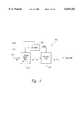
- the traditional approach to obtaining quadrature clock signalsis to use a clock generator 154 of the type shown in FIG. 2.
- the clock generator 154includes a first J-K flip flop 156 that generates the CLK signal and a second J-K flip-flop 158 that generates the CLK90 signal.
- a clock signal CLKAhaving twice the frequency of the quadrature clock signals CLK and CLK90 is applied to the clock input of the first flip-flop 156.
- the J and K inputs of the first flip-flop 156are coupled to a logic "1" voltage level so that the first flip-flop 156 toggles, as also shown in FIG. 3.
- the CLK signal generated at the Q output of the flip-flop 156transitions on each rising edge of the CLKA signal.
- the second J-K flip-flop 158is clocked by the inverse of the CLKA signal, which is generated at the output of an inverter 160 that receives the CLKA signal.
- the second flip-flop 158is also configured to toggle since its J and K inputs are coupled to a logic "1" voltage level.
- the CLK90 signal generated at the Q output of the flip-flop 158transitions on each falling edge of the CLKA signal.
- each J-K flip-flop 156, 158requires a great deal of circuitry to implement, thus increasing the size, complexity, and expense of memories and other devices using the J-K flip-flops 156, 158 to generate quadrature clock signals.
- the use of a clock generator 154 of the type shown in FIG. 2requires an input clock signal having twice the frequency of the quadrature clock signals CLK and CLK90 to toggle the flip flops 156, 158.
- CLK and CLK90the quadrature clock signals
- the present inventionis directed to a method and apparatus for generating multi-phase clock signals that may be used in the command generator of memory devices.
- the multi-phase clock generatorproduces on first and second output terminals respective first and second clock signals in which the second clock signal is delayed relative to the first clock signal.
- a coupling circuitcouples an input clock signal applied to an input terminal to the first output terminal of the clock generator.
- the input clock signalis also coupled to the input of a delay circuit having an output coupled to the second output terminal of the clock generator.
- the delay circuitdelays the input clock signal by a phase shift corresponding to more than 0 degrees and less than 180 degrees of the input clock signal.
- the first and second clock signals generated by the multi-phase clock generatormay be used in a clock circuit having a first gate, such as a NAND gate, operating according to an AND function, and a second gate, such as a NOR gate, operating according to an OR function.
- the first and second gateseach receive the first and second clock signals from the multi-phase clock generator to provide a pair of clocking signals.
- the clocking signalsmay drive a shift register so that data is shifted through the shift register on both the leading and falling edges of the input clock signal.
- the shift registermay be used in a packetized DRAM to sequentially store a plurality of command words. One or more of the resulting DRAMs may then be used in a computer system.
- FIG. 1is a block diagram of a SyncLink packetized dynamic random access memory (DRAM) that may advantageously use embodiments of the inventive clock generating circuit and method.
- DRAMSyncLink packetized dynamic random access memory
- FIG. 2is a logic diagram of a prior art circuit for generating quadrature clock signals that may be used in the memory of FIG. 1.
- FIG. 3is a timing diagram showing various signals present in the quadrature clock generating circuit of FIG. 2.
- FIG. 4is a block diagram of a command buffer that is usable in the packetized DRAM of FIG. 1.
- FIG. 5is a more detailed block diagram of a command buffer that is usable in the packetized DRAM of FIG. 1.
- FIG. 6is a timing diagram showing the clock signals used in a portion of the control circuit of the command buffer shown in FIGS. 4 and 5.
- FIG. 7is a logic diagram of one of the shift register circuits used in the command buffer shown in FIGS. 4 and 5.
- FIG. 8is a schematic and logic diagram of a shift register stage used in the shift register circuit of FIG. 7.
- FIG. 9is a timing diagram showing the various signals present in the shift register stage of FIG. 8.
- FIG. 10is a is a logic diagram of one embodiment of a circuit for generating multi-phase clock signals that may be used in the memory of FIG. 1.
- FIG. 11is a timing diagram showing various signals present in the multi-phase clock generating circuit of FIG. 10.
- FIG. 12is a block diagram of a computer system including a SyncLink memory device of the type shown in FIG. 1 and using the multiphase clock generator of FIG. 10 in its command buffer.
- FIG. 4One embodiment of a command buffer 46 that may use either the prior art quadrature clock generator clock generating circuit 154 of FIG. 2 or a multi-phase clock generating circuit in accordance with the invention is illustrated in FIG. 4.
- a command packet consisting of a plurality of packet wordsare applied to a shift register 202 via a bus 204.
- the width of the bus 204corresponds to the size of the shift register 202, and the number of packet words in the command packet corresponds to the number of stages of the shift register 202.
- the shift register 202has four stages each of which is 10 bits wide.
- the shift register 202sequentially receives four 10-bit packet words responsive to a clock signal CLK.
- a FLAG signalis applied to a control circuit 206 which is clocked by the CLK signal along with the shift register 202.
- the control circuit 206After four command words have been shifted into the shift register 202, the control circuit 206 generates a LOAD signal that is applied to a storage register 208.
- the storage register 208then loads all of the data stored in the shift register 202.
- the storage register 208receives and stores a 40-bit command word.
- the shift register 202has N stages, each of which has a width of M bits, and the storage register 208 loads an M*N bit command word.
- the storage register 208After the storage register 208 has been loaded, it continuously outputs the M*N bit command word.
- the command wordis used to control the operation of the memory 16 of FIG. 1.
- the manner in which the command buffer 46 performs this functionis described in detail in U.S. patent application Ser. No. 08/994,461 to Manning, which is incorporated herein by reference.
- the shift register 202 and the control circuit 206are shown in greater detail in FIG. 5.
- the control circuit 206generates a sequence of flag signals F ⁇ 0:7> that are used to control the operation of the memory 16. One of these flag signals F ⁇ 0:7> is used to load the contents of the shift register 202 into the storage register 208, as explained above.
- the control circuit 206also includes a clock circuit 230 that causes the packet words to be shifted through the shift register 202. As explained below, the clock circuit 230 uses a quadrature clock generator 231 to generate quadrature clock signals CLK and CLK 90 from the input clock signal CLKA.
- the quadrature clock generator 231may be either the prior art quadrature clock generator clock generating circuit 154 of FIG.
- the quadrature clock signals CLK and CLK90 generated by the quadrature clock generator 231are then used to generate two separate clock signals, CLK0 and CLK1, as well as their compliments, CLK0* and CLK1*, respectively.
- the shift register 202shifts each packet word through the shift register 202 on both the rising edge and the falling edge of the input clock signal CLKA.
- the CLK and CLK90 signalsare applied to a NOR gate 232 which outputs a high whenever CLK and CLK90 are both low, as illustrated in the timing diagram of FIG. 6.
- the output of the NOR gate 232is applied through a first inverter 234 to generate a CLK1 signal.
- the NOR gate 232 and the inverter 234 generating the CLK1 signalthus implement an OR gate.
- the output of the inverter 234is coupled through a second inverter 236 to generate a CLK1* signal (the "*" symbol after a signal name is used throughout to designate the compliment of the signal).
- the CLK90 and CLK signalsare also applied to a NAND gate 240 which outputs a low whenever both CLK and CLK90 are high, as also illustrated in FIG. 6.
- the output of the NAND gate 240is coupled through an inverter 242 to generate a CLK0 signal.
- the NAND gate 240 and the inverter 242 generating the CLK0 signalthus implement an AND gate.
- the output of the inverter 240is coupled through a second inverter 244 to generate a CLK0* signal.
- the control circuit 206also includes a pair of shift registers 246, 248 that are connected in series with each other to form an 8-stage shift register.
- the shift register 246receives the FLAG signal and sequentially shifts it through the four stages of the shift register circuit 246 and then through the four stages of the shift register circuit 248 responsive to the CLK0, CLK0*, CLK1, and CLK1* signals.
- the FLAG signalis shifted through two stages of the shift register circuits 246, 248 each cycle of the CLK signals.
- two successive F ⁇ 0:7> outputs of the shift register circuits 246, 248sequentially go high each clock cycle.
- the shift register 202 shown in FIG. 4includes ten separate shift register circuits 250a-j, each of which receive a respective bit CA0-CA9 of the incoming 10-bit packet word. As explained further below, each of the shift register circuits 250a-j includes four shift register stages. Thus, after four clock cycles, four packet word bits CA have been shifted into each shift register circuit 250, and all four of these bits are available as a 4-bit word B ⁇ 0:3>. Thus, the ten shift register circuits 250a-j collectively output a 40-bit command word.
- each of the shift registers 250a-jincludes four shift register stages 252a-d.
- the first stage 252areceives the packet word bit CA, and its output is connected to the input of the second stage 252b and to an external output B ⁇ 0>.
- each stage 252, until the last 252d,is connected to the input of a subsequent stage and to an external output. Transfer from the input to the output of each stage 252 is in response to four clock signals CLK0, CLK0*, CLK1, CLK1* as explained in greater detail below.
- CLK0, CLK0*, CLK1, CLK1*as explained in greater detail below.
- the ten shift register circuits 250a-jcollectively output a 40-bit command word.
- the shift register stages 252are shown in greater detail in FIG. 8. Each of the shift register stages 252 includes a first transfer gate 260, a second transfer gate 264, and a second latch 266.
- the transfer gate 260includes a first transfer gate circuit 270 operated by the CLK0 and CLK0* signals and a second transfer circuit 272 in parallel with the first transfer circuit 270 and operated by the CLK1 and CLK1* signals.
- the first latch 262 and the second latch 266are each formed by a pair of inverters 276, 278 connected input-to-output.
- the second transfer gate 264is formed by three PMOS transistors 280, 282, 284 connected between a supply voltage and the input to the second latch 266.
- the second transfer gate 264also includes three NMOS transistors 290, 292, 294 connected in series between the input to the second latch 266 and ground. As explained below, the second transfer gate 264 inverts the signal from the first latch 262. Therefore, to restore the correct phasing of the command signals CA, an inverter 298 is provided at the output of the second latch 266.
- Each of the transfer gate circuits 270, 272are formed by an NMOS transistor and a PMOS transistor (not shown) connected in parallel with each other with the gate of the NMOS transistor being coupled to the non-inverting input and the gate of the PMOS transistor coupled to the inverting input.
- the transfer gate circuit 270is conductive whenever the CLK0 signal is high and the CLK0* signal is low. Thus, the transfer gate circuit 270 is conductive for a short period each clock cycle, as shown by the line segments adjacent the 270 COND designation in FIG. 9. Similarly, the transfer gate 272 is conductive whenever the CLK1 signal is low and the CLK1* signal is high. As shown by the line segments in FIG. 8, the transfer gate circuit 272 is conductive for a short period each clock cycle, with the conductive period of the transfer gate circuit 270 being equally spaced from the conductive period of the transfer gate circuit 272.
- the first transfer gate 260is conductive twice each clock cycle, with each conductive period followed by a period of non-conductivity. Each time the transfer gate 260 is conductive, the inverse of the command bit CA is output from the latch 262 to the second transfer gate 264.
- the function of the second transfer gate 264is to couple the input to the second latch 266 to either V CC or ground at the proper time depending upon the value at the output of the first latch 262.
- the PMOS transistors 280, 282are conductive whenever CLK0 and CLK1* are both low, which occurs at times designated by the line segments adjacent the "PMOS" designation in FIG. 9.
- the NMOS transistors 292, 294are both conductive whenever the CLK1 signal and the CLK0* signal are both high, which occurs twice each clock cycle at the times designated by the line segments adjacent "NMOS" in FIG. 9.
- the PMOS transistors 280, 282 and the NMOS transistors 292, 294are all conductive at the same times, and these periods of conductivity alternate with the periods of conductivity of the first transfer gate 260.
- the input to the second latch 260is coupled to either V CC or ground during these periods of conductivity depending upon whether the output of the first latch 262 turns ON the PMOS transistor 284 or the NMOS transistor 290. More specifically, if the output of the first latch 262 is high, the NMOS transistor 290 will turn ON, thereby applying a low to the input of the second latch 266. If the output of the first latch 262 is low, the PMOS transistor 284 will turn ON, thereby applying a high to the input of the second latch 266.
- the second transfer gate 264couples the inverted output of the first latch 262 to the input of the second latch 266.
- the second latch 266outputs a signal that is the same as the output of the first latch 262 which, after passing through the inverter 298, is the same phase as the incoming command bit CA.
- the operation of the latch circuit 250is shown using a command bit CA, which is initially high, but goes low shortly after t 0 .
- the high command bit CAis transferred to the output of the first latch 262 in inverted form as shown in FIG. 9.
- the high at the output of the latch 262is coupled to the output of the latch 266, thereby causing the output to go low at time t 2 .
- the command bit CAgoes high.
- this highis coupled through the first latch 260, thereby causing the output of the second latch 262 to go low.
- the high output of the first latch 262is coupled to the output of the second latch 266, thereby causing the output to go high.
- a command bit coupled to the shift register stage 250is shifted to the output of the shift register stage 250 less than one clock cycle later.
- the command bitis shifted to the output of the next shift register stage until four clock cycles have elapsed, at which time four command bits have been shifted into each shift register circuit 250.
- two command bitsare shifted through each shift register circuit 250 each clock cycle in the same manner that the FLAG signal is shifted through two stages of the shift register circuit 246, 248 (FIG. 4) each clock cycle.
- the shift register circuits 250 shown in FIG. 7, including the shift register stages shown in FIG. 8,are also used as the shift registers 246, 248 in the control circuit 206 (FIG. 5).
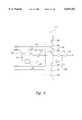
- FIG. 10One embodiment of a multi-phase clock generator 300 in accordance with the invention that may be used in the clock circuit 230 of FIG. 5 as the quadrature clock generator 231 is shown in FIG. 10.
- the clock generator 300is implemented by a conventional delay circuit 304 that receives the input clock signal CLKA and generates a delayed clock signal C-DEL.
- the delay circuit 304delays the input clock signal CLKA by substantially less than one-quarter of the period i.e., 90 degrees, of the input clock signal CLKA.
- the clock generator 300is able to function in the clock circuit 230' even though the phase shift produced by the delay circuit 304 differs somewhat from 90 degrees.
- the clock circuit 230'processes the CLKA and C-DEL signals in the same manner that the CLK and CLK90 signals are processed by the clock circuit 230, as explained above with reference to FIG. 5.
- the CLK1* signal generated at the output of the inverter 234is high whenever the CLKA and C-DEL signals are both low.
- the CLK0* signalis low whenever the CLKA and C-DEL signals are both high.
- the pass gate 270is therefor conductive whenever the CLKA and C-DEL signals are both high, and the pass gate 272 is conductive whenever the CLKA and C-DEL signals are both low.
- FIG. 8the pass gate 270 is therefor conductive whenever the CLKA and C-DEL signals are both high, and the pass gate 272 is conductive whenever the CLKA and C-DEL signals are both low.
- the PMOS transistors 280, 282 and the NMOS transistors 292, 294are all conductive whenever neither the pass gate 270 NOR the pass gate 272 are conductive.
- the command word bit CAis applied to the latch 262 when the pass gates 270, 272 are conductive, and then stored in the latch 270 and coupled through the transfer gate 264 when the pass gates 270, 272 are non-conductive.
- the only effect of the signal C-DEL being phase shifted by less than 90 degreesis that the conductive period of the pass gates 270, 272 is increased and the conductive period of the transfer gate 264 is decreased.
- the shift register stage 252will function properly as long as the phase shift of the signal C-DEL does not decrease too closely to 0 degrees or increase too closely to 180 degrees.
- the command word bit CAtransitions low at time t 0 .
- the pass gate 270becomes conductive and, at time t 2 , the transfer gate 264 couples the output of the latch 262 to the B output of the shift register stage 252.
- the clock circuit 230'causes the shift register stage 252 to shift each command word bit CA through the shift register 202 (FIG. 5).
- the clock generator 300 used in the clock circuit 230'is substantially less complex than the clock generator 154 of FIG. 2 that uses a pair of J-K flip-flops 156, 158 and an inverter 160.
- the command buffer 46 in the memory device 16 of FIG. 1may use the multi-phase clock generator 300 of FIG. 10, and the resulting memory device may be used in a computer system as shown in FIG. 12.
- the computer system 10includes a processor 12 having a processor bus 14 coupled to three packetized dynamic random access memory or SyncLink DRAMs ("SLDRAM") devices 16a-c of the type explained above with reference to FIG. 1.
- the computer system 10also includes one or more input devices 20, such as a keypad or a mouse, coupled to the processor 12 through a bus bridge 22 and an expansion bus 24, such as an industry standard architecture (“ISA”) bus or a Peripheral component interconnect (“PCI”) bus.
- the input devices 20allow an operator or an electronic device to input data to the computer system 10.
- One or more output devices 30are coupled to the processor 12 to display or otherwise output data generated by the processor 12.
- the output devices 30are coupled to the processor 12 through the expansion bus 24, bus bridge 22 and processor bus 14. Examples of output devices 24 include printers and a video display units.
- One or more data storage devices 38are coupled to the processor 12 through the processor bus 14, bus bridge 22, and expansion bus 24 to store data in or retrieve data from storage media (not shown). Examples of storage devices 38 and storage media include fixed disk drives floppy disk drives, tape cassettes and compact-disk read-only memory drives.
- the processor 12communicates with the memory devices 16a-c via the processor bus 14 by sending the memory devices 16a-c command packets that contain both control and address information.
- Datais coupled between the processor 12 and the memory devices 16a-c, through a data bus portion of the processor bus 14. Although all the memory devices 16a-c are coupled to the same conductors of the processor bus 14, only one memory device 16a-c at a time reads or writes data, thus avoiding bus contention on the processor bus 14. Bus contention is avoided by each of the memory devices 16a-c and the bus bridge 22 having a unique identifier, and the command packet contains an identifying code that selects only one of these components.
- the computer system 10also includes a number of other components and signal lines that have been omitted from FIG. 12 in the interests of brevity.
- the memory devices 16a-calso receive a master clock signal to provide internal timing signals, a data clock signal clocking data into and out of the memory device 16, and a FLAG signal signifying the start of a command packet.
Landscapes
- Physics & Mathematics (AREA)
- Engineering & Computer Science (AREA)
- Theoretical Computer Science (AREA)
- Nonlinear Science (AREA)
- General Engineering & Computer Science (AREA)
- General Physics & Mathematics (AREA)
- Dram (AREA)
Abstract
Description
Claims (33)
Priority Applications (1)
| Application Number | Priority Date | Filing Date | Title |
|---|---|---|---|
| US09/061,859US6029252A (en) | 1998-04-17 | 1998-04-17 | Method and apparatus for generating multi-phase clock signals, and circuitry, memory devices, and computer systems using same |
Applications Claiming Priority (1)
| Application Number | Priority Date | Filing Date | Title |
|---|---|---|---|
| US09/061,859US6029252A (en) | 1998-04-17 | 1998-04-17 | Method and apparatus for generating multi-phase clock signals, and circuitry, memory devices, and computer systems using same |
Publications (1)
| Publication Number | Publication Date |
|---|---|
| US6029252Atrue US6029252A (en) | 2000-02-22 |
Family
ID=22038612
Family Applications (1)
| Application Number | Title | Priority Date | Filing Date |
|---|---|---|---|
| US09/061,859Expired - LifetimeUS6029252A (en) | 1998-04-17 | 1998-04-17 | Method and apparatus for generating multi-phase clock signals, and circuitry, memory devices, and computer systems using same |
Country Status (1)
| Country | Link |
|---|---|
| US (1) | US6029252A (en) |
Cited By (30)
| Publication number | Priority date | Publication date | Assignee | Title |
|---|---|---|---|---|
| US6321282B1 (en) | 1999-10-19 | 2001-11-20 | Rambus Inc. | Apparatus and method for topography dependent signaling |
| US6360271B1 (en)* | 1999-02-02 | 2002-03-19 | 3Com Corporation | System for dynamic jitter buffer management based on synchronized clocks |
| US6366991B1 (en) | 1997-10-10 | 2002-04-02 | Micron Technology, Inc. | Method and apparatus for coupling signals between two circuits operating in different clock domains |
| US6434606B1 (en) | 1997-10-01 | 2002-08-13 | 3Com Corporation | System for real time communication buffer management |
| US6434684B1 (en)* | 1998-09-03 | 2002-08-13 | Micron Technology, Inc. | Method and apparatus for coupling signals across different clock domains, and memory device and computer system using same |
| US6452865B1 (en)* | 2001-08-09 | 2002-09-17 | International Business Machines Corporation | Method and apparatus for supporting N-bit width DDR memory interface using a common symmetrical read data path with 2N-bit internal bus width |
| US6560661B2 (en)* | 1997-04-25 | 2003-05-06 | Kabushiki Kaisha Toshiba | Data receiver that performs synchronous data transfer with reference to memory module |
| US6570813B2 (en) | 2001-05-25 | 2003-05-27 | Micron Technology, Inc. | Synchronous mirror delay with reduced delay line taps |
| US20030179027A1 (en)* | 2002-03-22 | 2003-09-25 | Kizer Jade M. | Locked loop with dual rail regulation |
| US20030183842A1 (en)* | 2002-03-22 | 2003-10-02 | Kizer Jade M. | System with phase jumping locked loop circuit |
| US6643787B1 (en) | 1999-10-19 | 2003-11-04 | Rambus Inc. | Bus system optimization |
| US6646953B1 (en) | 2000-07-06 | 2003-11-11 | Rambus Inc. | Single-clock, strobeless signaling system |
| US20040041604A1 (en)* | 2002-09-03 | 2004-03-04 | Kizer Jade M. | Phase jumping locked loop circuit |
| US20050052210A1 (en)* | 2003-09-05 | 2005-03-10 | Micron Technology, Inc. | Multiphase clock generators |
| US6922091B2 (en) | 2002-09-03 | 2005-07-26 | Rambus Inc. | Locked loop circuit with clock hold function |
| US20050172095A1 (en)* | 2004-01-29 | 2005-08-04 | Micron Technology, Inc. | Dual edge command in DRAM |
| US6952123B2 (en) | 2002-03-22 | 2005-10-04 | Rambus Inc. | System with dual rail regulated locked loop |
| US20060067157A1 (en)* | 2004-09-30 | 2006-03-30 | Hermann Ruckerbauer | Memory system with two clock lines and a memory device |
| US7051130B1 (en) | 1999-10-19 | 2006-05-23 | Rambus Inc. | Integrated circuit device that stores a value representative of a drive strength setting |
| US20080072092A1 (en)* | 2006-09-18 | 2008-03-20 | Samsung Electronics Co., Ltd. | System and method for tuning power consumption and group delay in wireless RFICs |
| US7570630B1 (en) | 2004-08-02 | 2009-08-04 | Sprint Spectrum L.P. | Dialed-digit based determination of whether to originate a call as a circuit-switched call or a packet-switched call |
| US20090226166A1 (en)* | 2001-02-05 | 2009-09-10 | Aronson Lewis B | Optoelectronic Transceiver with Digital Diagnostics |
| US8848480B1 (en)* | 2013-04-30 | 2014-09-30 | Freescale Semiconductor, Inc. | Synchronous multiple port memory with asynchronous ports |
| US8938062B2 (en) | 1995-12-11 | 2015-01-20 | Comcast Ip Holdings I, Llc | Method for accessing service resource items that are for use in a telecommunications system |
| US9191505B2 (en) | 2009-05-28 | 2015-11-17 | Comcast Cable Communications, Llc | Stateful home phone service |
| US10090026B2 (en)* | 2017-02-28 | 2018-10-02 | Micron Technology, Inc. | Apparatuses and methods for providing internal memory commands and control signals in semiconductor memories |
| US10210918B2 (en) | 2017-02-28 | 2019-02-19 | Micron Technology, Inc. | Apparatuses and methods for determining a phase relationship between an input clock signal and a multiphase clock signal |
| US10269397B2 (en) | 2017-08-31 | 2019-04-23 | Micron Technology, Inc. | Apparatuses and methods for providing active and inactive clock signals |
| US20200051603A1 (en)* | 2018-08-08 | 2020-02-13 | Micron Technology, Inc. | Clock signal drivers for read and write memory operations |
| US11526453B1 (en) | 2021-08-13 | 2022-12-13 | Micron Technology, Inc. | Apparatus including parallel pipelines and methods of manufacturing the same |
Citations (6)
| Publication number | Priority date | Publication date | Assignee | Title |
|---|---|---|---|---|
| US5173618A (en)* | 1990-05-14 | 1992-12-22 | Vlsi Technology, Inc. | Clock generator for providing a pair of nonoverlapping clock signals with adjustable skew |
| US5212716A (en)* | 1991-02-05 | 1993-05-18 | International Business Machines Corporation | Data edge phase sorting circuits |
| US5396111A (en)* | 1993-03-11 | 1995-03-07 | Data General Corporation | Clocking unit for digital data processing |
| US5497263A (en)* | 1992-09-10 | 1996-03-05 | Hitachi, Ltd. | Variable delay circuit and clock signal supply unit using the same |
| US5699005A (en)* | 1994-11-30 | 1997-12-16 | Deutsche Itt Industries Gmbh | Clock generator for generating a system clock causing minimal electromagnetic interference |
| US5929682A (en)* | 1996-05-09 | 1999-07-27 | International Business Machines Corp. | Clock signal generator, clock signal generating system, and clock pulse generation method |
- 1998
- 1998-04-17USUS09/061,859patent/US6029252A/ennot_activeExpired - Lifetime
Patent Citations (6)
| Publication number | Priority date | Publication date | Assignee | Title |
|---|---|---|---|---|
| US5173618A (en)* | 1990-05-14 | 1992-12-22 | Vlsi Technology, Inc. | Clock generator for providing a pair of nonoverlapping clock signals with adjustable skew |
| US5212716A (en)* | 1991-02-05 | 1993-05-18 | International Business Machines Corporation | Data edge phase sorting circuits |
| US5497263A (en)* | 1992-09-10 | 1996-03-05 | Hitachi, Ltd. | Variable delay circuit and clock signal supply unit using the same |
| US5396111A (en)* | 1993-03-11 | 1995-03-07 | Data General Corporation | Clocking unit for digital data processing |
| US5699005A (en)* | 1994-11-30 | 1997-12-16 | Deutsche Itt Industries Gmbh | Clock generator for generating a system clock causing minimal electromagnetic interference |
| US5929682A (en)* | 1996-05-09 | 1999-07-27 | International Business Machines Corp. | Clock signal generator, clock signal generating system, and clock pulse generation method |
Non-Patent Citations (4)
| Title |
|---|
| "Draft Standard for a High-Speed Memory Interface (SyncLink)," Microprocessor and Microcomputer Standards Subcommittee of the IEEE Computer Society, Copyright 1996 by the Institute of Electrical and Electronics Engineers, Inc., New York, NY, pp. 1-56. |
| Descriptive literature entitled, "400 MHz SLDRAM, 4M×16 SLDRAM Pipelined, Eight Bank, 2.5 V Operation," pp. 1-22. |
| Descriptive literature entitled, 400 MHz SLDRAM, 4M 16 SLDRAM Pipelined, Eight Bank, 2.5 V Operation, pp. 1 22.* |
| Draft Standard for a High Speed Memory Interface (SyncLink), Microprocessor and Microcomputer Standards Subcommittee of the IEEE Computer Society, Copyright 1996 by the Institute of Electrical and Electronics Engineers, Inc., New York, NY, pp. 1 56.* |
Cited By (119)
| Publication number | Priority date | Publication date | Assignee | Title |
|---|---|---|---|---|
| US8938062B2 (en) | 1995-12-11 | 2015-01-20 | Comcast Ip Holdings I, Llc | Method for accessing service resource items that are for use in a telecommunications system |
| US6560661B2 (en)* | 1997-04-25 | 2003-05-06 | Kabushiki Kaisha Toshiba | Data receiver that performs synchronous data transfer with reference to memory module |
| US6434606B1 (en) | 1997-10-01 | 2002-08-13 | 3Com Corporation | System for real time communication buffer management |
| US6366991B1 (en) | 1997-10-10 | 2002-04-02 | Micron Technology, Inc. | Method and apparatus for coupling signals between two circuits operating in different clock domains |
| US6434684B1 (en)* | 1998-09-03 | 2002-08-13 | Micron Technology, Inc. | Method and apparatus for coupling signals across different clock domains, and memory device and computer system using same |
| US6775755B2 (en) | 1998-09-03 | 2004-08-10 | Micron Technology, Inc. | Method and apparatus for coupling signals across different clock domains, and memory device and computer system using same |
| US6360271B1 (en)* | 1999-02-02 | 2002-03-19 | 3Com Corporation | System for dynamic jitter buffer management based on synchronized clocks |
| US9110828B2 (en) | 1999-10-19 | 2015-08-18 | Rambus Inc. | Chip having register to store value that represents adjustment to reference voltage |
| US7024502B2 (en) | 1999-10-19 | 2006-04-04 | Rambus Inc. | Apparatus and method for topography dependent signaling |
| US10366045B2 (en) | 1999-10-19 | 2019-07-30 | Rambus Inc. | Flash controller to provide a value that represents a parameter to a flash memory |
| US10310999B2 (en) | 1999-10-19 | 2019-06-04 | Rambus Inc. | Flash memory controller with calibrated data communication |
| US8102730B2 (en) | 1999-10-19 | 2012-01-24 | Rambus, Inc. | Single-clock, strobeless signaling system |
| US6643787B1 (en) | 1999-10-19 | 2003-11-04 | Rambus Inc. | Bus system optimization |
| US8001305B2 (en) | 1999-10-19 | 2011-08-16 | Rambus Inc. | System and dynamic random access memory device having a receiver |
| US8214570B2 (en) | 1999-10-19 | 2012-07-03 | Rambus Inc. | Memory controller and method utilizing equalization co-efficient setting |
| US20030231537A1 (en)* | 1999-10-19 | 2003-12-18 | Stark Donald C. | Single-clock, strobeless signaling system |
| US6684263B2 (en) | 1999-10-19 | 2004-01-27 | Rambus Inc. | Apparatus and method for topography dependent signaling |
| US8458385B2 (en) | 1999-10-19 | 2013-06-04 | Rambus Inc. | Chip having register to store value that represents adjustment to reference voltage |
| US20100146321A1 (en)* | 1999-10-19 | 2010-06-10 | Rambus Inc. | Single-clock, strobeless signaling system |
| US20040076192A1 (en)* | 1999-10-19 | 2004-04-22 | Rambus Inc. | Calibrated data communication system and method |
| US20040098634A1 (en)* | 1999-10-19 | 2004-05-20 | Zerbe Jared Levan | Integrated circuit with timing adjustment mechanism and method |
| US9852105B2 (en) | 1999-10-19 | 2017-12-26 | Rambus Inc. | Flash controller to provide a value that represents a parameter to a flash memory |
| US20040139257A1 (en)* | 1999-10-19 | 2004-07-15 | Rambus Inc. | Apparatus and method for topography dependent signaling |
| US6516365B2 (en) | 1999-10-19 | 2003-02-04 | Rambus Inc. | Apparatus and method for topography dependent signaling |
| US20040199690A1 (en)* | 1999-10-19 | 2004-10-07 | Rambus Inc. | Apparatus and method for topography dependent signaling |
| US7663966B2 (en) | 1999-10-19 | 2010-02-16 | Rambus, Inc. | Single-clock, strobeless signaling system |
| US20040243753A1 (en)* | 1999-10-19 | 2004-12-02 | Rambus Inc. | Memory device having programmable drive strength setting |
| US9785589B2 (en) | 1999-10-19 | 2017-10-10 | Rambus Inc. | Memory controller that calibrates a transmit timing offset |
| US20090327789A1 (en)* | 1999-10-19 | 2009-12-31 | Zerbe Jared Levan | Memory System with Calibrated Data Communication |
| US9411767B2 (en) | 1999-10-19 | 2016-08-09 | Rambus Inc. | Flash controller to provide a value that represents a parameter to a flash memory |
| US20050141335A1 (en)* | 1999-10-19 | 2005-06-30 | Rambus Inc. | Single-clock, strobeless signaling system |
| US9405678B2 (en) | 1999-10-19 | 2016-08-02 | Rambus Inc. | Flash memory controller with calibrated data communication |
| US9323711B2 (en) | 1999-10-19 | 2016-04-26 | Rambus Inc. | Chip having port to receive value that represents adjustment to transmission parameter |
| US20090248971A1 (en)* | 1999-10-19 | 2009-10-01 | Horowitz Mark A | System and Dynamic Random Access Memory Device Having a Receiver |
| US6950956B2 (en) | 1999-10-19 | 2005-09-27 | Rambus Inc. | Integrated circuit with timing adjustment mechanism and method |
| US8630317B2 (en) | 1999-10-19 | 2014-01-14 | Rambus Inc. | Memory system with calibrated data communication |
| US9164933B2 (en) | 1999-10-19 | 2015-10-20 | Rambus Inc. | Memory system with calibrated data communication |
| US6982922B2 (en) | 1999-10-19 | 2006-01-03 | Rambus Inc. | Single-clock, strobeless signaling system |
| US6990042B2 (en) | 1999-10-19 | 2006-01-24 | Rambus Inc. | Single-clock, strobeless signaling system |
| US9152581B2 (en) | 1999-10-19 | 2015-10-06 | Rambus Inc. | Chip storing a value that represents adjustment to output drive strength |
| US8170067B2 (en) | 1999-10-19 | 2012-05-01 | Rambus Inc. | Memory system with calibrated data communication |
| US7032057B2 (en) | 1999-10-19 | 2006-04-18 | Rambus Inc. | Integrated circuit with transmit phase adjustment |
| US7042914B2 (en) | 1999-10-19 | 2006-05-09 | Rambus Inc. | Calibrated data communication system and method |
| US20060104151A1 (en)* | 1999-10-19 | 2006-05-18 | Rambus Inc. | Single-clock, strobeless signaling system |
| US7051130B1 (en) | 1999-10-19 | 2006-05-23 | Rambus Inc. | Integrated circuit device that stores a value representative of a drive strength setting |
| US7051129B2 (en) | 1999-10-19 | 2006-05-23 | Rambus Inc. | Memory device having programmable drive strength setting |
| US20060120409A1 (en)* | 1999-10-19 | 2006-06-08 | Zerbe Jared L | Calibrated data communication system and method |
| US9135967B2 (en) | 1999-10-19 | 2015-09-15 | Rambus Inc. | Chip having register to store value that represents adjustment to output drive strength |
| US9135186B2 (en) | 1999-10-19 | 2015-09-15 | Rambus Inc. | Chip having port to receive value that represents adjustment to output driver parameter |
| US6321282B1 (en) | 1999-10-19 | 2001-11-20 | Rambus Inc. | Apparatus and method for topography dependent signaling |
| US20080052440A1 (en)* | 1999-10-19 | 2008-02-28 | Horowitz Mark A | Integrated Circuit Memory Device and Signaling Method with Topographic Dependent Signaling |
| US20080052434A1 (en)* | 1999-10-19 | 2008-02-28 | Rambus Inc. | Integrated Circuit Device and Signaling Method with Topographic Dependent Equalization Coefficient |
| US8948212B2 (en) | 1999-10-19 | 2015-02-03 | Rambus Inc. | Memory controller with circuitry to set memory device-specific reference voltages |
| US20080071951A1 (en)* | 1999-10-19 | 2008-03-20 | Horowitz Mark A | Integrated Circuit Device and Signaling Method with Phase Control Based on Information in External Memory Device |
| US7397725B2 (en) | 1999-10-19 | 2008-07-08 | Rambus Inc. | Single-clock, strobeless signaling system |
| US7565468B2 (en) | 1999-10-19 | 2009-07-21 | Rambus Inc. | Integrated circuit memory device and signaling method for adjusting drive strength based on topography of integrated circuit devices |
| US7535933B2 (en) | 1999-10-19 | 2009-05-19 | Rambus Inc. | Calibrated data communication system and method |
| US8775705B2 (en) | 1999-10-19 | 2014-07-08 | Rambus Inc. | Chip having register to store value that represents adjustment to reference voltage |
| US7539802B2 (en) | 1999-10-19 | 2009-05-26 | Rambus Inc. | Integrated circuit device and signaling method with phase control based on information in external memory device |
| US7546390B2 (en) | 1999-10-19 | 2009-06-09 | Rambus, Inc. | Integrated circuit device and signaling method with topographic dependent equalization coefficient |
| US20080267000A1 (en)* | 1999-10-19 | 2008-10-30 | Rambus Inc. | Single-clock, strobeless signaling system |
| US6646953B1 (en) | 2000-07-06 | 2003-11-11 | Rambus Inc. | Single-clock, strobeless signaling system |
| US9577759B2 (en) | 2001-02-05 | 2017-02-21 | Finisar Corporation | Method of monitoring an optoelectronic transceiver with multiple flag values for a respective operating condition |
| US20090226166A1 (en)* | 2001-02-05 | 2009-09-10 | Aronson Lewis B | Optoelectronic Transceiver with Digital Diagnostics |
| US9184850B2 (en) | 2001-02-05 | 2015-11-10 | Finisar Corporation | Method of monitoring an optoelectronic transceiver with multiple flag values for a respective operating condition |
| US8515284B2 (en) | 2001-02-05 | 2013-08-20 | Finisar Corporation | Optoelectronic transceiver with multiple flag values for a respective operating condition |
| US8849123B2 (en) | 2001-02-05 | 2014-09-30 | Finisar Corporation | Method of monitoring an optoelectronic transceiver with multiple flag values for a respective operating condition |
| US10291324B2 (en) | 2001-02-05 | 2019-05-14 | Finisar Corporation | Method of monitoring an optoelectronic transceiver with multiple flag values for a respective operating condition |
| US8086100B2 (en) | 2001-02-05 | 2011-12-27 | Finisar Corporation | Optoelectronic transceiver with digital diagnostics |
| US6570813B2 (en) | 2001-05-25 | 2003-05-27 | Micron Technology, Inc. | Synchronous mirror delay with reduced delay line taps |
| US6822925B2 (en) | 2001-05-25 | 2004-11-23 | Micron Technology, Inc. | Synchronous mirror delay with reduced delay line taps |
| US20040057331A1 (en)* | 2001-05-25 | 2004-03-25 | Micron Technology, Inc. | Synchronous mirror delay with reduced delay line taps |
| US6665232B2 (en) | 2001-05-25 | 2003-12-16 | Micron Technology, Inc. | Synchronous mirror delay with reduced delay line taps |
| US6643219B2 (en) | 2001-05-25 | 2003-11-04 | Micron Technology, Inc. | Synchronous mirror delay with reduced delay line taps |
| US6452865B1 (en)* | 2001-08-09 | 2002-09-17 | International Business Machines Corporation | Method and apparatus for supporting N-bit width DDR memory interface using a common symmetrical read data path with 2N-bit internal bus width |
| US6952123B2 (en) | 2002-03-22 | 2005-10-04 | Rambus Inc. | System with dual rail regulated locked loop |
| US6960948B2 (en) | 2002-03-22 | 2005-11-01 | Rambus Inc. | System with phase jumping locked loop circuit |
| US7902890B2 (en) | 2002-03-22 | 2011-03-08 | Rambus Inc. | Locked loop circuit with clock hold function |
| US20030179027A1 (en)* | 2002-03-22 | 2003-09-25 | Kizer Jade M. | Locked loop with dual rail regulation |
| US20030183842A1 (en)* | 2002-03-22 | 2003-10-02 | Kizer Jade M. | System with phase jumping locked loop circuit |
| US20090219067A1 (en)* | 2002-03-22 | 2009-09-03 | Rambus Inc. | Locked Loop Circuit With Clock Hold Function |
| US8680903B2 (en) | 2002-03-22 | 2014-03-25 | Rambus Inc. | Locked loop circuit with clock hold function |
| US6759881B2 (en) | 2002-03-22 | 2004-07-06 | Rambus Inc. | System with phase jumping locked loop circuit |
| US20050001662A1 (en)* | 2002-03-22 | 2005-01-06 | Kizer Jade M. | System with phase jumping locked loop circuit |
| US6911853B2 (en) | 2002-03-22 | 2005-06-28 | Rambus Inc. | Locked loop with dual rail regulation |
| US7535271B2 (en) | 2002-03-22 | 2009-05-19 | Rambus Inc. | Locked loop circuit with clock hold function |
| US8120399B2 (en) | 2002-03-22 | 2012-02-21 | Rambus Inc. | Locked loop circuit with clock hold function |
| US20050206416A1 (en)* | 2002-03-22 | 2005-09-22 | Kizer Jade M | Locked loop circuit with clock hold function |
| US6922091B2 (en) | 2002-09-03 | 2005-07-26 | Rambus Inc. | Locked loop circuit with clock hold function |
| US7135903B2 (en) | 2002-09-03 | 2006-11-14 | Rambus Inc. | Phase jumping locked loop circuit |
| US20040041604A1 (en)* | 2002-09-03 | 2004-03-04 | Kizer Jade M. | Phase jumping locked loop circuit |
| US20050052210A1 (en)* | 2003-09-05 | 2005-03-10 | Micron Technology, Inc. | Multiphase clock generators |
| US20050172095A1 (en)* | 2004-01-29 | 2005-08-04 | Micron Technology, Inc. | Dual edge command in DRAM |
| US9324391B2 (en) | 2004-01-29 | 2016-04-26 | Micron Technology, Inc. | Dual event command |
| US7549033B2 (en) | 2004-01-29 | 2009-06-16 | Micron Technology, Inc. | Dual edge command |
| US7299329B2 (en) | 2004-01-29 | 2007-11-20 | Micron Technology, Inc. | Dual edge command in DRAM |
| US9767886B2 (en) | 2004-01-29 | 2017-09-19 | Micron Technology, Inc. | Memory command received within two clock cycles |
| US20090248970A1 (en)* | 2004-01-29 | 2009-10-01 | Choi Joo S | Dual edge command |
| US7570630B1 (en) | 2004-08-02 | 2009-08-04 | Sprint Spectrum L.P. | Dialed-digit based determination of whether to originate a call as a circuit-switched call or a packet-switched call |
| US7173877B2 (en)* | 2004-09-30 | 2007-02-06 | Infineon Technologies Ag | Memory system with two clock lines and a memory device |
| US20060067157A1 (en)* | 2004-09-30 | 2006-03-30 | Hermann Ruckerbauer | Memory system with two clock lines and a memory device |
| US20080072092A1 (en)* | 2006-09-18 | 2008-03-20 | Samsung Electronics Co., Ltd. | System and method for tuning power consumption and group delay in wireless RFICs |
| US7844847B2 (en)* | 2006-09-18 | 2010-11-30 | Samsung Electronics Co., Ltd. | System and method for tuning power consumption and group delay in wireless RFICs |
| US9191505B2 (en) | 2009-05-28 | 2015-11-17 | Comcast Cable Communications, Llc | Stateful home phone service |
| US8848480B1 (en)* | 2013-04-30 | 2014-09-30 | Freescale Semiconductor, Inc. | Synchronous multiple port memory with asynchronous ports |
| US10210918B2 (en) | 2017-02-28 | 2019-02-19 | Micron Technology, Inc. | Apparatuses and methods for determining a phase relationship between an input clock signal and a multiphase clock signal |
| US10825495B2 (en) | 2017-02-28 | 2020-11-03 | Micron Technology, Inc. | Apparatuses and methods for determining a phase relationship between an input clock signal and a multiphase clock signal |
| TWI665683B (en)* | 2017-02-28 | 2019-07-11 | 美商美光科技公司 | Apparatuses and methods for providing internal memory commands and control signals in semiconductor memories |
| US10090026B2 (en)* | 2017-02-28 | 2018-10-02 | Micron Technology, Inc. | Apparatuses and methods for providing internal memory commands and control signals in semiconductor memories |
| US10515676B2 (en) | 2017-02-28 | 2019-12-24 | Micron Technology, Inc. | Apparatuses and methods for determining a phase relationship between an input clock signal and a multiphase clock signal |
| US10534394B2 (en) | 2017-02-28 | 2020-01-14 | Micron Technology, Inc. | Apparatuses and methods for providing internal memory commands and control signals in semiconductor memories |
| US10984844B2 (en) | 2017-02-28 | 2021-04-20 | Micron Technology, Inc. | Apparatuses and methods for determining a phase relationship between an input clock signal and a multiphase clock signal |
| US10860469B2 (en) | 2017-02-28 | 2020-12-08 | Micron Technology, Inc. | Apparatuses and methods for providing internal memory commands and control signals in semiconductor memories |
| US10269397B2 (en) | 2017-08-31 | 2019-04-23 | Micron Technology, Inc. | Apparatuses and methods for providing active and inactive clock signals |
| US10872646B2 (en) | 2017-08-31 | 2020-12-22 | Micron Technology, Inc. | Apparatuses and methods for providing active and inactive clock signals |
| US10937473B2 (en)* | 2018-08-08 | 2021-03-02 | Micron Technology, Inc. | Clock signal drivers for read and write memory operations |
| US20200051603A1 (en)* | 2018-08-08 | 2020-02-13 | Micron Technology, Inc. | Clock signal drivers for read and write memory operations |
| US11526453B1 (en) | 2021-08-13 | 2022-12-13 | Micron Technology, Inc. | Apparatus including parallel pipelines and methods of manufacturing the same |
| US12265485B2 (en) | 2021-08-13 | 2025-04-01 | Micron Technology, Inc. | Apparatus including parallel pipelines and methods of manufacturing the same |
Similar Documents
| Publication | Publication Date | Title |
|---|---|---|
| US6029252A (en) | Method and apparatus for generating multi-phase clock signals, and circuitry, memory devices, and computer systems using same | |
| EP1010179B1 (en) | Two step memory device command buffer apparatus and method and memory devices and computer systems using same | |
| US6301322B1 (en) | Balanced dual-edge triggered data bit shifting circuit and method | |
| US6952462B2 (en) | Method and apparatus for generating a phase dependent control signal | |
| US6496440B2 (en) | Method and system for accessing rows in multiple memory banks within an integrated circuit | |
| US8565008B2 (en) | Method and apparatus for generating a sequence of clock signals | |
| US6434684B1 (en) | Method and apparatus for coupling signals across different clock domains, and memory device and computer system using same | |
| US5825711A (en) | Method and system for storing and processing multiple memory addresses | |
| US6338127B1 (en) | Method and apparatus for resynchronizing a plurality of clock signals used to latch respective digital signals, and memory device using same | |
| US6366991B1 (en) | Method and apparatus for coupling signals between two circuits operating in different clock domains | |
| US6279090B1 (en) | Method and apparatus for resynchronizing a plurality of clock signals used in latching respective digital signals applied to a packetized memory device | |
| US6094727A (en) | Method and apparatus for controlling the data rate of a clocking circuit | |
| US6175905B1 (en) | Method and system for bypassing pipelines in a pipelined memory command generator | |
| US6175894B1 (en) | Memory device command buffer apparatus and method and memory devices and computer systems using same | |
| KR100703584B1 (en) | Adjustable double-edge triggered data bit shifting circuit and method | |
| JP4678471B2 (en) | Circuit and method of balanced dual edge triggered data bit shift |
Legal Events
| Date | Code | Title | Description |
|---|---|---|---|
| AS | Assignment | Owner name:MICRON TECHNOLOGY, INC., IDAHO Free format text:ASSIGNMENT OF ASSIGNORS INTEREST;ASSIGNOR:MANNING, TROY A.;REEL/FRAME:009106/0509 Effective date:19980401 | |
| STCF | Information on status: patent grant | Free format text:PATENTED CASE | |
| CC | Certificate of correction | ||
| FPAY | Fee payment | Year of fee payment:4 | |
| FPAY | Fee payment | Year of fee payment:8 | |
| FPAY | Fee payment | Year of fee payment:12 | |
| AS | Assignment | Owner name:U.S. BANK NATIONAL ASSOCIATION, AS COLLATERAL AGENT, CALIFORNIA Free format text:SECURITY INTEREST;ASSIGNOR:MICRON TECHNOLOGY, INC.;REEL/FRAME:038669/0001 Effective date:20160426 Owner name:U.S. BANK NATIONAL ASSOCIATION, AS COLLATERAL AGEN Free format text:SECURITY INTEREST;ASSIGNOR:MICRON TECHNOLOGY, INC.;REEL/FRAME:038669/0001 Effective date:20160426 | |
| AS | Assignment | Owner name:MORGAN STANLEY SENIOR FUNDING, INC., AS COLLATERAL AGENT, MARYLAND Free format text:PATENT SECURITY AGREEMENT;ASSIGNOR:MICRON TECHNOLOGY, INC.;REEL/FRAME:038954/0001 Effective date:20160426 Owner name:MORGAN STANLEY SENIOR FUNDING, INC., AS COLLATERAL Free format text:PATENT SECURITY AGREEMENT;ASSIGNOR:MICRON TECHNOLOGY, INC.;REEL/FRAME:038954/0001 Effective date:20160426 | |
| AS | Assignment | Owner name:U.S. BANK NATIONAL ASSOCIATION, AS COLLATERAL AGENT, CALIFORNIA Free format text:CORRECTIVE ASSIGNMENT TO CORRECT THE REPLACE ERRONEOUSLY FILED PATENT #7358718 WITH THE CORRECT PATENT #7358178 PREVIOUSLY RECORDED ON REEL 038669 FRAME 0001. ASSIGNOR(S) HEREBY CONFIRMS THE SECURITY INTEREST;ASSIGNOR:MICRON TECHNOLOGY, INC.;REEL/FRAME:043079/0001 Effective date:20160426 Owner name:U.S. BANK NATIONAL ASSOCIATION, AS COLLATERAL AGEN Free format text:CORRECTIVE ASSIGNMENT TO CORRECT THE REPLACE ERRONEOUSLY FILED PATENT #7358718 WITH THE CORRECT PATENT #7358178 PREVIOUSLY RECORDED ON REEL 038669 FRAME 0001. ASSIGNOR(S) HEREBY CONFIRMS THE SECURITY INTEREST;ASSIGNOR:MICRON TECHNOLOGY, INC.;REEL/FRAME:043079/0001 Effective date:20160426 | |
| AS | Assignment | Owner name:MICRON TECHNOLOGY, INC., IDAHO Free format text:RELEASE BY SECURED PARTY;ASSIGNOR:U.S. BANK NATIONAL ASSOCIATION, AS COLLATERAL AGENT;REEL/FRAME:047243/0001 Effective date:20180629 | |
| AS | Assignment | Owner name:MICRON TECHNOLOGY, INC., IDAHO Free format text:RELEASE BY SECURED PARTY;ASSIGNOR:MORGAN STANLEY SENIOR FUNDING, INC., AS COLLATERAL AGENT;REEL/FRAME:050937/0001 Effective date:20190731 |