US6028564A - Wire antenna with optimized impedance for connecting to a circuit - Google Patents
Wire antenna with optimized impedance for connecting to a circuitDownload PDFInfo
- Publication number
- US6028564A US6028564AUS08/790,640US79064097AUS6028564AUS 6028564 AUS6028564 AUS 6028564AUS 79064097 AUS79064097 AUS 79064097AUS 6028564 AUS6028564 AUS 6028564A
- Authority
- US
- United States
- Prior art keywords
- antenna
- impedance
- stub
- loading
- wavelength
- Prior art date
- Legal status (The legal status is an assumption and is not a legal conclusion. Google has not performed a legal analysis and makes no representation as to the accuracy of the status listed.)
- Expired - Lifetime
Links
Images


Classifications
- G—PHYSICS
- G06—COMPUTING OR CALCULATING; COUNTING
- G06K—GRAPHICAL DATA READING; PRESENTATION OF DATA; RECORD CARRIERS; HANDLING RECORD CARRIERS
- G06K19/00—Record carriers for use with machines and with at least a part designed to carry digital markings
- G06K19/06—Record carriers for use with machines and with at least a part designed to carry digital markings characterised by the kind of the digital marking, e.g. shape, nature, code
- G06K19/067—Record carriers with conductive marks, printed circuits or semiconductor circuit elements, e.g. credit or identity cards also with resonating or responding marks without active components
- G06K19/07—Record carriers with conductive marks, printed circuits or semiconductor circuit elements, e.g. credit or identity cards also with resonating or responding marks without active components with integrated circuit chips
- G06K19/077—Constructional details, e.g. mounting of circuits in the carrier
- G06K19/07749—Constructional details, e.g. mounting of circuits in the carrier the record carrier being capable of non-contact communication, e.g. constructional details of the antenna of a non-contact smart card
- G06K19/07773—Antenna details
- G06K19/07786—Antenna details the antenna being of the HF type, such as a dipole
- H—ELECTRICITY
- H01—ELECTRIC ELEMENTS
- H01Q—ANTENNAS, i.e. RADIO AERIALS
- H01Q1/00—Details of, or arrangements associated with, antennas
- H01Q1/36—Structural form of radiating elements, e.g. cone, spiral, umbrella; Particular materials used therewith
- H—ELECTRICITY
- H01—ELECTRIC ELEMENTS
- H01Q—ANTENNAS, i.e. RADIO AERIALS
- H01Q9/00—Electrically-short antennas having dimensions not more than twice the operating wavelength and consisting of conductive active radiating elements
- H01Q9/04—Resonant antennas
- H01Q9/16—Resonant antennas with feed intermediate between the extremities of the antenna, e.g. centre-fed dipole
Definitions
- This inventionrelates to the field of antenna design. More specifically, the invention relates to the field of optimizing the terminal voltage of an antenna attached to a circuit and the power transferred from an electromagnetic field to the circuit through the antenna, especially when the antenna is used in radio frequency tags.
- FIG. 1is a graph of the output voltage of a typical antenna and front end circuit.
- the antennaproduces a voltage when excited by an electromagnetic field. This voltage is commonly called the open-circuit voltage across the antenna terminals.
- the antenna terminalsWhen the antenna terminals are connected to a front end circuit, power is transferred from the electromagnetic field through the antenna and into the front end circuits (front end).
- Front endsare generally known in the art and are used to convert (or down convert) the AC electromagnetic field into an intermediate frequency (IF) or direct current (DC) frequency.
- IFintermediate frequency
- DCdirect current
- FIG. 1shows the voltage output of a front end and antenna combination versus frequency of the electromagnetic field.
- This voltage outputhas two regions: 1. a flat region 110 over a wide range of frequencies that produces a relatively low voltage output, and 2. a resonant region or bandwidth 120 centered about a resonant frequency 125 where the antenna produces a relatively large voltage over a smaller frequency range.
- the antenna/front end combinationis designed to disturb an electromagnetic field as little as possible.
- a field sensormeasures the strength of an electromagnetic field and typically uses small antennas that operate over the wide frequency band 110, i.e., not around a resonant frequency 125 of the field sensor antenna. Over the range of frequencies 110, the front end is tuned so that it is out of resonance with the antenna. Therefore, there is a minimum of power taken by the combination, i.e., there is a minimum of power transferred from the antenna to the front end.
- Another way of stating thisis that the antenna is loaded with a mismatched load (front end) that limits how much the electromagnetic field can excite the antenna.
- the combinationis equally sensitive over a wide frequency range 110 and draws a minimum amount of power from the field, i.e., the sensor perturbs the field a minimum amount.
- the antenna resonant frequencyis chosen to be well outside the operation frequency range 110 and the front end is designed so that the combination does not resonate in the operation frequency range 110.
- antennasoperate over the bandwidth 120 to receive/transmit signals over as wide a bandwidth as required.
- the bandwidth 120 of the antennais relatively narrow but is widened in some cases, e.g., in television, radio, and some radar systems, to transmit/receive over a large number of channels or over a wide continuous spectrum.
- antenna designersnarrow the bandwidth 120 as needed to comply with the requirements.
- the front endis designed to resonate with the antenna over the operation frequency range 120 so that the maximum amount of power is transferred between the antenna (and hence the electromagnetic field) and the front end (and hence any circuitry attached to the front end).
- the front endis variably tunable over a plurality of frequencies 125 so that the operation frequency range 120 varies over the frequency scale 130.
- RFIDradio frequency identification
- RFID circuits connected to the front end and the rest of the RFID circuitneed to produce a front end output voltage that is above a threshold voltage, in order to power the RFID circuit. This is typically accomplished by trying to match the antenna impedance to that of the front end of the RFID circuit (e.g. a chip) at the resonance frequency 125.
- These front end circuitstypically use diode and capacitor circuits (the front end) that rectify the radio frequency (RF) carrier component of the modulated electromagnetic field, that excites the antenna, leaving the modulated signal (envelope) at the output of the front end.
- RFradio frequency
- directors and/or reflectorsIn general radio and TV applications, some prior art uses directors and/or reflectors to match the antenna impedance to a transmission line. However, the major effect of this solution is to give the antenna a more directional radiation pattern. However, since directors/reflectors typically are spaced at a large fraction of the resonant wavelength (e.g. 0.4 lambda, the carrier frequency wavelength), this solution requires large amounts of space in the antenna circuit package.
- the antenna/front end combinationhas to produce a minimum output voltage to power the chip and to provide a sufficient power collected from the electromagnetic field to provide current to the RFID circuit. If the voltage and/or power requirements of the RFID circuit are not fulfilled, the circuit will not operate. If the antenna/front end combination is not optimal, it will have a limited range (distance) over which it can communicate.
- the prior artattempts to match the antenna and front end impedances in a variety of ways.
- the prior artuses impedance matching circuits using discrete components, e.g., inductor/capacitor networks.
- the impedance matching circuitcan comprise distributed elements such as microstrip structures. These alternatives add cost and size to the RFID circuit package.
- An object of this inventionis an improved antenna apparatus.
- An object of this inventionis an improved antenna apparatus, used in combination with a radio frequency front end, that can be tuned to produce an optimal voltage output and power transfer.
- An object of this inventionis an improved antenna apparatus, used in combination with a radio frequency front end, that can be tuned to produce an optimal voltage output and power transfer with a minimal dimensional constraints on the antenna.
- An object of this inventionis an improved antenna apparatus, used in combination with a radio frequency front end, that can be tuned to produce an optimal voltage and power transfer without using additional discrete components in the front end.
- This inventionis an antenna used as a voltage and power source that is designed to operate with arbitrary load, or front end.
- the inventionis particularly useful where it is difficult and/or costly to change the load (front end) design, e.g., in the field of communicating with RFID circuits.
- the antennapreferably a dipole antenna, has one or more (number of) loading bars that are placed adjacent to the elements of the antenna at a spacing distance.
- the real part of the antenna input impedanceis changed by adjusting the loading bar length, width, and/or spacing distance and/or the number of loading bars. These changes are implemented to reduce the real part of the antenna input impedance to make it small enough to develop an adequate voltage, Vp, to operate the front end and connected circuitry.
- the real part of the antenna input impedanceis reduced to the point at which Vp no longer increases.
- one or more stubsis added to one or more of the antenna elements.
- the stubsact as two-conductor transmission line that is terminated either in a short-circuit or open-circuit.
- the short-circuited stub(s)acts as a lumped inductor (capacitor) when the length of the transmission line is within odd (even) multiples of one quarter "guided wavelength" of the transmission line.
- the guided wavelengthhas a known relation to the wavelength to which the antenna is tuned.
- the open-circuited stub(s)acts as a lumped capacitor (inductor) when the length of the transmission line is within odd (even) multiples of one quarter of the guided wavelength.
- the magnitude of these lumped capacitors and inductorsis affected not only by the material surrounding the stub, but also is affected by a stub length, a stub conductor width, and a stub conductor spacing.
- Zero or more short-circuit stubs and zero or more open-circuit stubsare added to one or more of the antenna elements to change the reactive (imaginary) part of the antenna input impedance.
- the reactive part of the antenna input impedanceis changed to equal the negative magnitude of the reactive part of the front end input impedance. This gives the maximum voltage, VDC, for a given real part (Ra) of the antenna input impedance and the maximum power transfer between the antenna and the front end.
- the loading barchanges vary the real part of the antenna input impedance.
- the length of the antennacan change (increase or decrease) to change the reactive part of the antenna impedance while changing the real part of the antenna impedance only a minimal amount.
- adding the stubschanges the reactive part of the antenna input impedance while the real part of the antenna input impedance changes only a minimal amount. Therefore, the invention essentially decouples the tuning of the real part and reactive part of the antenna input impedance and permits effective antenna design to optimize the combination of the antenna and any arbitrary front end (impedance).
- FIG. 1is a graph showing a prior art representation of the frequency response of a prior art antenna/front end combination.
- FIG. 2is a block diagram of a radio frequency transmitter (FIG. 2A) communicating an RF signal to a receiver (FIG. 2B).
- FIG. 3is a block diagram of a preferred antenna and front end combination (FIG. 3A) and a general equivalent circuit of this combination (FIG. 3B).
- FIG. 4is a block diagram showing one novel structure of the present antenna using one or more loading bars.
- FIG. 5comprising FIGS. 5A-5D, shows variations of the loading bar structures.
- FIG. 6,is a block diagram showing an short-circuit (FIG. 6A) and an open-circuit stub (FIG. 6B) structure.
- FIG. 7,comprising FIGS. 7A and 7B, shows variations of the stub structures.
- FIG. 8is a diagram showing preferred dipole antenna with both loading bars and a stub structure.
- FIG. 9is a diagram showing an alternative preferred meander dipole with a single loading bar and stub structure.
- FIG. 2is a block diagram showing a system 200 with a transmitter or base station 210 communicating an RF signal 220 to any general receiver 230, specifically an RFID tag 230.
- Block 210is any radio frequency transmitter/transponder that is well known in the art.
- the transmitterincludes an RF source 211 and RF amplifier 212 that sends RF power to the transmitter antenna 215.
- the transmitter 210can also have an optional receiver section 218 for two way communications with the receiver/tag 230.
- the transmitter 210transmits an RF signal 220 with a transmitter carrier frequency.
- the transmitter carrieralso has a transmitting carrier frequency bandwidth referred to as a transmitting bandwidth. The transmitting bandwidth will be wide enough to transmit data at a rate selected by the system designer.
- Systems like thisare well known in the art. See for example U.S. patent application Ser. No. 4,656,463 to Anders et al. entitled "LIMIS Systems, Devices and Methods", issued on Apr. 7, 1987 which is herein incorporated by reference in its entirety.
- FIG. 2Bis a block diagram of a receiver 230, specifically an RFID tag, comprising the present novel antenna 250 (see FIG. 4), an RF processing section, i.e., the front end, 232 and a signal processing section 234.
- the antenna 250 and front end 232make up the antenna/front end combination 260.
- the front end 232can be any known front end design used with an antenna. Typically, in RFID applications using passive tags, the front end 232 converts the electromagnetic field 220 into a direct current (DC) voltage that supplies the power required to operate the signal processing component 234 of the RFID circuit (232 and 234 inclusive) and extracts the envelop of the modulated signal from the electromagnetic field 220. Examples of front ends are well known. See for example the Hewlett Packard "Communications Components GaAs & Silicon Products Designer's Catalog" (for instance pages 2-15) which is herein incorporated by reference in its entirety. A preferred front end is shown in FIG. 3A.
- the signal processing component 234 of the RFID circuitcan be any known RFID circuit. Examples of this processing component are given in U.S. patent application Ser. No. 08/694,606, entitled “Radio Frequency Identification System with Write Broadcast Capability” to Heinrich et al. filed on Aug. 9, 1996, and U.S. patent application Ser. No. 08/681,741, entitled “Radio Frequency Identification Transponder with Electronic Circuit Enabling/Disabling Capability”, filed Jul. 29, 1996, which are both herein incorporated by reference in its entirety.
- FIG. 3Ais a block diagram showing a preferred front end 332 and the novel antenna 250.
- the antennacomprises a dipole antenna 340 with one or more optional stubs 350 on one or both of its elements (340A and 340B).
- One or more loading bars 360are placed close and parallel to the dipole 340 elements (340A, 340B).
- Alternative embodiments of the antenna 250are described below.
- the front end 332is electrically connected to the antenna 250.
- the front end 332comprises diodes D1, D2, and D3, and capacitors Cp and Cs.
- the diodes D1, D2, and D3have a low series resistance and a low parasitic capacitance.
- the series resistanceis less than 30 ohms and the parasitic capacitance is less than 500 femto farads.
- these diodesare Schottky diodes that are produced by known semiconductor processing techniques.
- the capacitors, Cp and Csare also produced by known semiconductor processing techniques.
- capacitors, Cp and Cscan be discrete devices.
- Diodes D1 and D2 and capacitor Cpform a voltage doubler circuit that rectifies the electromagnetic field 220 into a DC voltage that stores energy in the capacitor Cp used to power the signal processing component 234. Therefore, a voltage, Vp, is developed across capacitor Cp.
- diodes D1 and D2produce the voltage Vp that is equal to or less than 2 times the voltage, Voc, produced across the antenna terminals (370A, 370B), where Voc is the open-circuit voltage produced at the antenna terminals (370A, 370B) from the electromagnetic field 220.
- Vocis an AC voltage
- Vpis a DC voltage.
- the magnitude of Vpis equal to or less than the peak to peak value of Voc. See U.S.
- the capacitor, Cpis large enough to be treated as a short-circuit at the carrier frequency of the electromagnetic field 220 and large enough to store enough energy to power the signal processing component 234.
- the value of Cpis between 10 pf and 500 pf for a 2.44 gigaHertz (GHz) carrier frequency.
- Diodes D1 and D3 and capacitor Csform a second voltage doubler circuit that also rectifies the electromagnetic field 220 into a DC voltage that stores energy in the capacitor Cs used to provide a demodulated signal to the signal processing component 234. Therefore, a DC voltage, Vs, is developed across capacitor Cs.
- the DC voltage or low frequency AC voltage, Vsis the signal voltage that is equal to or less than 2 times the amplitude of the AC voltage, Voc, produced across the antenna terminals (370A, 370B), where Voc is the open-circuit voltage produced from the electromagnetic field 220.
- the capacitor, Csis large enough to be treated as a short-circuit at the carrier frequency of the electromagnetic field 220 but should be small enough so that signal is not smoothed to the point where it can not be used by the signal processing component 234.
- the value of Csis between 1.5 pf and 25 pf for a carrier frequency of 2.44 gigaHertz and a signal frequency of 38.4 kiloHertz. More preferably the range of Cs is between 1.5 pf and 10 pf.
- the carrier frequencydetermines the lower boundary and the signal frequency determines the upper boundary for the value of Cs.
- FIG. 3Bis a circuit diagram of a circuit 390 that models the combination 260 of the antenna 250 and the front end 332.
- the circuitcomprises a voltage, Voc; an antenna impedance, Za; and a front end impedance, Zc.
- the voltage, Voc, and the impedance, Zarepresent the equivalent circuit of the antenna 250, while the impedance, Zc, represents the equivalent circuit of the front end.
- the impedance, Za (Zc)has a real part Ra (Rc) and an imaginary part Xa (Xc), respectively.
- the impedance Za, and therefore its real, Ra, and imaginary, Xa, parts,are uniquely determined by the components (340, 350, 360) of the antenna 250 and their respective physical dimensions.
- the dimensions of the antenna elements (340A, 340B), the stub 350, and the loading bar(s) 360are chosen so that the DC voltage developed in the front end, e.g. Vp and Vs, and the power transferred to the front end, e.g. stored in capacitors Cp and Cs, is optimum for an arbitrarily selected front end 232.
- the optimum voltageis the voltage, Vp, necessary to power the signal processing component 234 at a given distance from the base station antenna 215 and the optimum power is the maximum possible power transferred under this voltage condition. This is accomplished, for any arbitrary front end, while maintaining the resonant frequency of the antenna and minimizing the area and volume that the antenna 250 occupies.
- the inventionfurther permits the antenna 250 to be designed for a narrow bandwidth.
- the problem solved by this inventionis how to design a power source, i.e., an antenna 250 given an arbitrary load 232.
- This problemarises in one instance where it is difficult and/or costly to change the load design, e.g., the design of the RFID circuit (including the front end 232) used with the antenna 250.
- This problemhas not been recognized or addressed by the prior art, particularly in the field of RFID.
- the voltage provided to the load, the RFID circuite.g., either Vp or Vs, is given by
- ⁇is the voltage multiplying factor, e.g., 2 for a front end with a voltage doubler, 4 for a quadrupler, etc. This equation neglects the "turn on” (offset) voltage of the diodes.
- the voltage VDCis maximum when the imaginary part of the antenna impedance, Xa, and the imaginary part of the front end impedance, Xc, cancel, and the real part of the antenna impedance, Ra, is minimum, i.e., zero.
- the real part of the antenna impedance, Racan not be zero. This is because as Ra approaches zero, so does the open circuit voltage, Voc, generated by the antenna. Furthermore, as Ra approaches zero, the amount of energy back scattered from the antenna also approaches zero and, as a result, no data can be transmitted back to the base station 210.
- the power transferred to the loadis proportional to the square of Voc, the power available to the load (RFID circuit) falls as the square of Voc.
- the voltage, Vocis determined by the following:
- the loading bar 360is added to the dipole 340 to reduce the real part of the antenna impedance, Ra.
- one or more loading bars 360are added to reduce Ra to a minimum value.
- this minimum valuemust be large enough to: 1. maintain Voc above a minimum input voltage, 2. maintain a minimum power to the load to provide the current required by the load, and 3. to provide enough back scattered 221 electromagnetic field to transmit information to the base station 210, if required.
- Rais reduced from about 73 ohms to about 15 ohms.
- Rais further reduced to less than 10 ohms.
- the minimum voltage, Vocis determined by the requirements to operate the arbitrarily selected load, e.g. RFID circuit (232,234), at a given distance 240 from the base station. Since Voc is the product of heff and Ei, heff must be maintained above a minimum level given the Ei (i.e., the distance and field 220 strength) and the voltage requirements of the load. For some CMOS processes, Vp must be above 1.5 volts to read data from an Electrically Erasable Programmable Read Only Memory an (EEPROM) and other Complementary Metal Oxide Semiconductor (CMOS) circuit, and typically between 3 and 3.3 volts to write to an EEPROM circuit. These voltages will be reduced in finer line-width processes.
- EEPROMElectrically Erasable Programmable Read Only Memory
- CMOSComplementary Metal Oxide Semiconductor
- Poweris proportional to the square of Voc and if Voc drops too low, there will not be an adequate amount of current for the load. This requirement is determined by the minimum current requirements of the load. In a preferred embodiment, several micro amperes are required to read an EEPROM circuit and ten times that level of current is required to write to an EEPROM circuit. Therefore, the antenna must maintain the respective Voc described above while delivering these required currents.
- the (optional) back scattering requirementis determined by the distance 240, the sensitivity of the base station receiver 218, the power transmitted, and back scattering cross section (a function of Ra) of the antenna, the gain of the base station antenna, and the gain of the tag antenna, as follows: ##EQU1## where R is the maximum detection range (e.g. 240), P min is the minimum power required for the receiver 218 to detect the signal (determined by the sensitivity of the receiver 218), P t is the transmitted power transmitted by the RF source 211, G is the gain of the base station antenna 215, ⁇ is the wavelength of the RF signal 220, and ⁇ is the effective absorbing area of the antenna 250.
- Ris the maximum detection range (e.g. 240)
- P minis the minimum power required for the receiver 218 to detect the signal (determined by the sensitivity of the receiver 218)
- P tis the transmitted power transmitted by the RF source 211
- Gis the gain of the base station antenna 215
- ⁇is the wavelength of the
- Rais in the range between 10 ohms and 73 ohms and more preferably in the range between 10 ohms and 25 ohms.
- the stub 350is provided to adjust the imaginary part (reactance) of the antenna, Xa, to cancel the effect of the imaginary part of the load, Xc.
- the stub 350adjusts Xa to be inductive with the same magnitude as Xc.
- the length of the dipole elements (340A, 340B)can also be adjusted to achieve this cancellation.
- the resonant frequency of the antennaalso changes and the size of the antenna typically increases.
- increasing the length of the antenna elements (340A, 340B)causes the real part of the antenna impedance, Ra, to increase rapidly and therefore reduce the voltage (and power) to the load.
- the reactance of the antennacan be adjusted to cancel any arbitrary load reactance, Xc, without increasing the size of the antenna, without increasing the real part of the antenna impedance (therefore not reducing the voltage and power to the load), and without substantially changing the resonant frequency of the antenna.
- the effective height of the antenna 250, heffcan be maintained virtually unchanged, when the stub(s) 350 is (are) introduced.
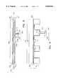
- FIG. 4is a block diagram of one preferred embodiment of the present receiving antenna 250, e.g. mounted on a substrate.
- the substratecan be any known substrate and the antenna any type of an conductive material, e.g. metal wires, printed metal on circuit (PC) boards, printed metal on flexible substrate, screen printed conductive ink, and punched (or etched) lead frame.
- conductive materiale.g. metal wires, printed metal on circuit (PC) boards, printed metal on flexible substrate, screen printed conductive ink, and punched (or etched) lead frame.
- PCprinted metal on circuit
- One preferred method and apparatus that can be used with the design of this antennais disclosed in U.S. patent application Ser. Nos. 08/621,784 entitled “Thin Radio Frequency Transponder with Leadframe Antenna Structure", filed on Mar. 25, 1996 to Brady et al. and 08/621/385 entitled “Method of Making Thin Radio Frequency Transponder” filed on Mar. 25, 1996 to Brady et al. which
- FIG. 4shows a dipole antenna 400 with a number 450 of (one or more) loading bars (360,410).
- Various geometric properties of the loading barinclude: the length of a loading bar(s) 420, the width of a loading bar(s) 430, the distance 440 between a loading bar and the antenna 400, and the distance 460 between loading bars when there is more than one loading bar. Thickness of the conductive lamination, not shown, is not considered significant for these applications. Where the cross sections of the conductive lamination are of different non-rectangular shapes, known analysis can be used to determine an equivalent lamination with a rectangular cross section. Note that for most RFID applications, the thickness of the conductive lamination is a small percentage of the width of the antenna 401 or loading bars 410 and therefore, these cross sectional effects is of secondary importance.
- the antenna (250, 400)is shown as a dipolar antenna.
- the inventionwill also apply to other well known antenna types, e.g., folded dipole, loop antenna or their complements (slot antennas).
- slot antennasFor examples of some antenna types, see U.S. patent application Ser. No. 08/303,976 to Brady et al., titled “RADIO FREQUENCY IDENTIFICATION TAG", filed on Sep. 9, 1994, and U.S. Pat. No. 5,528,222 to Moskowitz et al. issued Jun. 18, 1996 which are both herein incorporated by reference in their entirety.
- the front endIn the cases where the antenna is not a DC open-circuit, the front end must be designed to provide a DC isolation (e.g. inserting an appropriate capacitor in series with the antenna and its terminal 370 ).
- Complements of antennasare those antennas where the conductive portion is replaced by non conductive material and the non conductive portion is replaced by conductive material.
- a number 450, i.e., one or more, loading bars 410are placed adjacent (within a distance 440) to the antenna 400 so that, in combination, they act as a loading element on the antenna 400.
- a loading bar 410is characterized by its length 420, width 430, and the distance 440 to the antenna 400.
- the effect of loading bars 410is to suppress (reduce) the real part of the antenna input impedance, Ra. This suppression is observed over a bandwidth.
- the real part of the antenna input impedance, Rarises again, but at a slower rate compared to the antenna 400 with no loading bar 410.
- the presence of the loading bar 410also affects the imaginary part of the antenna input impedance. However, the effect is minimal, and the imaginary part of the antenna input impedance still increases monotonically as frequency increases. Therefore, over the bandwidth, the Ra is suppressed without significantly affecting the imaginary part.
- the spacing 440 between the loading bars and the antenna 400the more significant is the suppression of the real part of the antenna input impedance, Ra.
- the spacing 440is less than 25% of the the wavelength of the operating frequency, i.e., the frequency 125 to which the antenna is tuned to resonate. In a more preferred embodiment, the spacing 440 is less than 10% of this wavelength, and in a still more preferred embodiment, the spacing 440 is less than 3% of this wavelength.
- the resonant frequency(the frequency at which the imaginary part of the antenna input impedance vanishes) decreases when the spacing 440 between the loading bar and a dipole antenna increases. The change in resonant frequency is also minor. For instance, the antenna can be retuned by changing the length of the antenna 400 but this change in length (on the order of a few per cent) will not cause the antenna 400 to occupy a much larger area.
- the length of loading bars 420is between zero and the length of the antenna 400, the suppression effect increases as the length 420 increases.
- the length 420here is the effective length, i.e., the length of the loading bar that is within the spacing distance 440 of the antenna and therefore has a stronger interaction with the antenna.
- the effectis less significant when the length 420 becomes larger than the length 405 of the antenna 400.
- the length of loading bars 420is chosen to be similar to or smaller than that of a dipole antenna, e.g. the length of the dipole, within a tolerance. Manufacturing considerations may also dictate the length 420.
- the effect of loading barsincreases with the width 430 of loading bars, namely, the real part of the antenna input impedance is further suppressed.
- Empirical testshave shown that loading bar widths 430 of up to 30 times the width 401 of the antenna effectively suppress the real part, Ra.
- a loading bar with the same width 430 as that of the antenna 401will suppress Ra.
- a single loading bar with a width 430 equal to the width of the antenna 401, a length 420 approximately equal to the length 405 of the antenna, and a spacing 440 of twice the antenna width 401suppressed Ra from 73 ohms to 15 ohms.
- increasing the width 430 of the loading barfurther reduces Ra.
- the real part of the antenna input impedanceis suppressed more with a larger number of loading bars 550.
- a second loading bar 410 with the same width 430 as the antenna's width 401 and a spacing 460 to the first loading barthe same as the spacing 440 between the first loading bar 410 and the antenna 400 suppressed the Ra from 15 ohms to 5 ohms.
- the number of bars 450depends on the application, two preferred numbers of bars 450 are: one or two. The smaller the number 450 of loading bars 410, the less area the antenna occupies and the less asymmetry is introduced into the antenna radiation pattern.
- the spacing 460 between the loading bars 410is chosen to be similar to that between loading bars and the antenna 440, i.e., less than 25% of the wavelength. Note that the further that the next loading bar is from the antenna, the less the effect on Ra of this loading bar. Also, this loading bar spacing 460 can be varied to affect the antenna radiation pattern.
- the length of loading bars 420, the width of loading bars 430, the spacing to a dipole antenna 440, and the number of loading bars 450can be adjusted to obtain the desired real part of the antenna input impedance without significantly changing the imaginary part of the antenna input impedance, Xa, and the resonant frequency of the antenna 400.
- FIG. 5is a block diagram that shows alternative embodiments of the loading bars 410.
- the loading bars 410are adjacent to the antenna 400. "Adjacent" means that at least some part (i.e., the effective part) of the the loading bar is within a distance 440 of some part of the antenna 400, where the distance 440 is a small percentage (preferably under 25%, more preferably under 10%, and still more preferably under 3%) of the wavelength of the resonant and/or operating frequency.
- FIG. 5Ashows loading bars 410 of various shapes. Note that any combination of these shapes is possible.
- Loading bar 510is a non-linear loading bar, e.g. having one or more curves.
- Loading bar 520is linear.
- Loading bar 530has one or more locations with a varying width 430.
- Loading bar 535is made of two or more sections that are not electrically connected to one another. Note that at one or more points along the loading bars 410, e.g., the ends, two or more loading bars can be electrically connected. In some embodiments, this might be done to enhance the mechanical strength of the antenna 400.
- FIG. 5Bshows loading bars (510, 532) on either or both sides of a dipole antenna 400.
- FIG. 5Cshows a loading bar 540 that wraps around the antenna 400.
- FIG. 5Dshows loading bars with various lengths (420 A,B), various spacing between the loading bars (460 A,B), and various widths of loading bars
- the loading effect of the loading barsis caused by the accumulated effect of the electromagnetic coupling between any given point on the loading bar 410 to any given point on the antenna 400 as well as the electromagnetic coupling among the loading bars.
- This couplingis inversely proportional to the distance between these two points. Therefore, there are the following rules of thumb:
- FIG. 6Ais a block diagram of a closed- or short-circuited tuning stub 600 that is part of one or more of the elements of the antenna 400.
- FIG. 6Bshows an alternative tuning stub, the short- or open-circuited tuning stub 650. Closed tuning stubs 600 and open tuning stubs 650 add reactance to the antenna and therefore, can be treated as a lumped reactive element (inductor or capacitor).
- Tuning stubsare further disclosed and claimed in U.S. patent application Ser. No. ber XXX, entitled “A WIRE ANTENNA WITH STUBS TO OPTIMIZE IMPEDANCE FOR CONNECTING TO A CIRCUIT” filed on the same day as this disclosure.
- a tuning stubmay be treated as a transmission line comprising two transmission-line conductors 610 and a termination 620.
- a tuning stubcan be treated as a lumped, reactive circuit element, namely, an inductor or a capacitor.
- the electrical property of the tuning stubis determined by its length 612, width of the conductors 614, spacing of the conductors 616, and a termination 620.
- the termination 620could be a short-circuited termination 622, or an open-circuited termination 624.
- the impedance of a stubis determined by
- Z0is the characteristic impedance of the stub transmission line
- tanis the tangent trigonometrical function
- betais the phase constant of the stub transmission line
- lis the length of the stub 612.
- logis the natural logarithm function
- sis the center-to-center spacing of the transmission line conductors 616
- wis the width of the transmission line conductors 614.
- phase constant of the stub transmission line, betais determined by
- lambda_gis the guided wavelength that is related to the medium that surrounds the antenna.
- the guided wavelengthcan be determined by well known techniques.
- Piis approximately equal to 3.1416.
- the impedance of a stubis given by
- jis the square root of -1
- Z0is the characteristic impedance of the stub transmission line
- cotis the cotangent trigonometrical function
- betais the phase constant of the stub transmission line
- 1is the length of the stub 612.
- the length of a tuning stub 612is often constrained to be shorter than a quarter of a guided wavelength in the transmission line.
- the imaginary part of the impedance of a short-circuited stubis positive according to equation (1), making the stub behave like an inductor.
- the imaginary part of the impedance of an open-circuited stubis negative according to equation (4), making the stub behave like a capacitor. Notice that if the length of the stub 612 is between a quarter wavelength and a half wave length, a short-circuited stub becomes capacitive, and an open-circuited stub becomes inductive.
- the reactance of the tuning stubchanges sign when the length of the stub changes into the next quarter wavelength.
- the stub lengths 612are less than or equal to a quarter wave length of the operating/resonance frequency. However, this description applies equally to other quarter wavelength multiples of length as described above.
- the length 612, spacing 616, and termination of the stub (620, 624), and the substrate materialcan be chosen to produce the desired reactance value.
- the substrate materialchanges the effective dielectric constant that determines the characteristic impedance of the transmission line 610.
- the tuning stubbasically behaves like a lumped circuit element. It may be used to replace a lumped inductor, for example, to load an antenna and to produce the desired antenna input impedance without significantly changing Ra.
- a tuning stubfunctions independently of the loading bars. While loading bars mainly change the real part of the antenna input, Ra, the tuning stubs mainly change the reactive part of the antenna input impedance.
- FIG. 7shows variations of the use of tuning stubs. Note that the tuning stubs can be used independently of loading bars.
- FIG. 7(a)shows a dipole antenna containing multiple tuning stubs. Further, the stubs can have different geometrical parameters, e.g. spacing 116, width 614, length 612, termination (620, 624), and material. For example, the stub 710 has a wider separation 116A and a shorter length 612A than the separation 116B and length 612B of stub 720.
- FIG. 7(b)shows tuning stubs on both arms (340A, 340B) of a dipole antenna 250. One or more of the stubs on each of the arms 340 can have different geometrical parameters than those on the other arm 340. The stubs can also be placed 720 on opposite sides of either of the arms 340.
- FIG. 8is a block diagram of one preferred embodiment of the antenna 250.
- the width 801 of the antennathere are two 850 loading bars, each with a width 830 that is the same as the width 801 of the antenna.
- this width 801is chosen to be between 0.25 to 0.75 millimeters (mm), preferably about 0.5 mm. These numbers are chosen mainly for manufacturing convenience.
- the first loading baris spaced from the antenna at a distance 840 that is equal to about 2 times the antenna width 801.
- the second loading baris equally spaced at the same distance 860 from the first loading bar.
- the length 820 of the loading barsare chosen to be equal to that of the antenna mainly for manufacturing convenience. However, this configuration causes the antenna radiation pattern to be asymmetric.
- the lengths of the loading bars 820are shortened to make the pattern more symmetric. Note that while reducing the length of the loading bars 820 affects both the antenna radiation pattern symmetry and Ra, the magnitude of the effect on symmetry is greater than that on Ra.
- the loading bar length 820can be between 70 and 100 percent of the antenna length (about 50 mm) without changing Ra significantly.
- Racan be "tuned” by changing the other geometrical parameters of the loading bars as described above. Other geometric parameters, e.g. the number of loading bars 850, also will affect the radiation pattern.
- a single stub 880is placed at a distance 806 from the antenna connection 870. This distance 806 has little effect on the antenna input impedance for most of the length of the antenna. However, the distance 806 is chosen so that the stub is not too close to the end of the arm of the dipole because placement at the end of the dipole would cause the stub to be at a current minimum. If the distance 806 is within 70 per cent of the antenna arm length the antenna impedance will not change significantly with respect to the position of a given stub 880. However, in the 30 per cent of the antenna arm length that is at the end of the dipole, there is a noticeable change in antenna impedance with respect to the position of a given stub 880 in this region. Therefore, in this embodiment, the stub 880 is located at a 806 within 70 per cent of the antenna length for ease of tuning the antenna.
- the single stub 880has a line width 814 that is one half of the width of the antenna 801.
- the center-to-center spacing 816is about the same as the antenna line width 801.
- the transmission line length 812is about 10 percent of the antenna length (which is slightly less than 1/2 wavelength).
- the termination 820is a short-circuit which causes the stub 880 to be inductive.
- FIG. 9is a diagram showing an alternative preferred embodiment of a meander dipole with a single loading bar and stub structure.
- Meander dipoleshave arms that are not straight lines and are well known in the literature.
- the length of the antenna(not numbered) can be placed in a smaller area.
- This embodimentuses a single 950 loading bar with a width 930 that is the same as the antenna line width 901.
- the loading baris placed at a distance 940 from a given point on the antenna that is the same as the antenna line width 901.
- the length of the loading bar 920is the same as the linear distance 925 spanned by the meander dipole.
- a single stub 980is located on one of the arms of the meander dipole at a distance 906 from the antenna terminal 370 that is within 70 percent of the linear distance 925 spanned by the meander dipole.
- the transmission line length 912is chosen, as before, to be about 10 percent of the entire (meandered) antenna length.
- the stub width 914is equal to the line width 901 of the antenna.
- the stub spacing 916is equal to twice the line width 901 of the antenna.
- the terminationis a short-circuit so that the stub appears as a lumped inductor. (Note that the stub is drawn as pointing downward.) However, the same effect can be achieved by a stub that is pointing up or by a stub that is placed horizontally at one of the vertical sections of the meander dipole.
Landscapes
- Engineering & Computer Science (AREA)
- Computer Networks & Wireless Communication (AREA)
- Computer Hardware Design (AREA)
- Microelectronics & Electronic Packaging (AREA)
- Physics & Mathematics (AREA)
- General Physics & Mathematics (AREA)
- Theoretical Computer Science (AREA)
- Variable-Direction Aerials And Aerial Arrays (AREA)
Abstract
Description
VDC=
γVoc|Rc+jXc|/|Ra+Rc+j(Xa+Xc)|=.gamma.VL
Voc=heff * Ei
Zs=j*Z0*tan(beta*1) (1)
Z0=120*log(4*s/w) (2)
beta=2*pi/lambda_g (3)
Zo=-j*Z0*cot(beta*1) (4)
Claims (26)
Priority Applications (1)
| Application Number | Priority Date | Filing Date | Title |
|---|---|---|---|
| US08/790,640US6028564A (en) | 1997-01-29 | 1997-01-29 | Wire antenna with optimized impedance for connecting to a circuit |
Applications Claiming Priority (1)
| Application Number | Priority Date | Filing Date | Title |
|---|---|---|---|
| US08/790,640US6028564A (en) | 1997-01-29 | 1997-01-29 | Wire antenna with optimized impedance for connecting to a circuit |
Publications (1)
| Publication Number | Publication Date |
|---|---|
| US6028564Atrue US6028564A (en) | 2000-02-22 |
Family
ID=25151313
Family Applications (1)
| Application Number | Title | Priority Date | Filing Date |
|---|---|---|---|
| US08/790,640Expired - LifetimeUS6028564A (en) | 1997-01-29 | 1997-01-29 | Wire antenna with optimized impedance for connecting to a circuit |
Country Status (1)
| Country | Link |
|---|---|
| US (1) | US6028564A (en) |
Cited By (61)
| Publication number | Priority date | Publication date | Assignee | Title |
|---|---|---|---|---|
| US6147606A (en)* | 1998-03-26 | 2000-11-14 | Intermec Ip Corp. | Apparatus and method for radio frequency transponder with improved read distance |
| US6177872B1 (en)* | 1998-03-13 | 2001-01-23 | Intermec Ip Corp. | Distributed impedance matching circuit for high reflection coefficient load |
| US6215402B1 (en)* | 1998-03-13 | 2001-04-10 | Intermec Ip Corp. | Radio frequency identification transponder employing patch antenna |
| US6373440B2 (en) | 2000-05-31 | 2002-04-16 | Bae Systems Information And Electronic Systems Integration, Inc. | Multi-layer, wideband meander line loaded antenna |
| US6480110B2 (en)* | 2000-12-01 | 2002-11-12 | Microchip Technology Incorporated | Inductively tunable antenna for a radio frequency identification tag |
| US6535175B2 (en)* | 2000-06-01 | 2003-03-18 | Intermec Ip Corp. | Adjustable length antenna system for RF transponders |
| US20040075607A1 (en)* | 2000-04-26 | 2004-04-22 | Cathey David A. | Automated antenna trim for transmitting and receiving semiconductor devices |
| US20040080462A1 (en)* | 2002-10-23 | 2004-04-29 | Apostolos John T. | Stagger tuned meanderline loaded antenna |
| US6759917B2 (en)* | 2000-04-07 | 2004-07-06 | Matsushita Electric Industrial Co., Ltd. | Method and apparatus for adjusting impedance of matching circuit |
| US20040135726A1 (en)* | 2001-05-24 | 2004-07-15 | Adi Shamir | Method for designing a small antenna matched to an input impedance, and small antennas designed according to the method |
| US20040178912A1 (en)* | 1999-09-02 | 2004-09-16 | Smith Freddie W. | Remote communication devices, radio frequency identification devices, wireless communication systems, wireless communication methods, radio frequency identification device communication methods, and methods of forming a remote communication device |
| US20050024287A1 (en)* | 2003-05-29 | 2005-02-03 | Young-Min Jo | Radio frequency identification tag |
| US20050041624A1 (en)* | 2003-06-03 | 2005-02-24 | Ping Hui | Systems and methods that employ a dualband IFA-loop CDMA antenna and a GPS antenna with a device for mobile communication |
| US20050040994A1 (en)* | 2003-08-22 | 2005-02-24 | Checkpoint Systems, Inc. | Security tag with three dimensional antenna array made from flat stock |
| US6903656B1 (en)* | 2003-05-27 | 2005-06-07 | Applied Wireless Identifications Group, Inc. | RFID reader with multiple antenna selection and automated antenna matching |
| US6947007B1 (en)* | 2000-08-21 | 2005-09-20 | Synergy Microwave Corporation | Shortened dipole and monopole loops |
| WO2005088770A1 (en) | 2004-03-05 | 2005-09-22 | Koninklijke Philips Electronics N.V. | Antenna configuration for rfid tags |
| US20050242964A1 (en)* | 1992-08-12 | 2005-11-03 | Tuttle John R | Miniature radio frequency transceiver |
| US20050270243A1 (en)* | 2004-06-05 | 2005-12-08 | Caimi Frank M | Meanderline coupled quadband antenna for wireless handsets |
| US20060132360A1 (en)* | 2004-10-15 | 2006-06-22 | Caimi Frank M | Method and apparatus for adaptively controlling antenna parameters to enhance efficiency and maintain antenna size compactness |
| US20060158380A1 (en)* | 2004-12-08 | 2006-07-20 | Hae-Won Son | Antenna using inductively coupled feeding method, RFID tag using the same and antenna impedence matching method thereof |
| US20060220869A1 (en)* | 2005-03-15 | 2006-10-05 | Intermec Ip Corp. | Tunable RFID tag for global applications |
| US20060250250A1 (en)* | 2005-05-04 | 2006-11-09 | Youn Tai W | RFID tag with small aperture antenna |
| US20060281423A1 (en)* | 2004-10-15 | 2006-12-14 | Caimi Frank M | Methods and Apparatuses for Adaptively Controlling Antenna Parameters to Enhance Efficiency and Maintain Antenna Size Compactness |
| US20070018904A1 (en)* | 1998-02-04 | 2007-01-25 | Smith Freddie W | Communication devices, communication systems and methods of communicating |
| US20070023525A1 (en)* | 2005-07-27 | 2007-02-01 | Hae-Won Son | Open-ended two-strip meander line antenna, RFID tag using the antenna, and antenna impedance matching method thereof |
| US20070080869A1 (en)* | 2005-10-12 | 2007-04-12 | Benq Corporation | Antenna structure on circuit board |
| EP1826711A1 (en)* | 2006-02-24 | 2007-08-29 | Fujitsu Limited | RFID tag |
| WO2007096789A1 (en) | 2006-02-24 | 2007-08-30 | Nxp B.V. | Transmitter, receiver, antenna arrangement for use with a transmitter or for use with a receiver, and rfid transponder |
| US20070222697A1 (en)* | 2004-10-15 | 2007-09-27 | Caimi Frank M | Methods and Apparatuses for Adaptively Controlling Antenna Parameters to Enhance Efficiency and Maintain Antenna Size Compactness |
| US20070273473A1 (en)* | 1997-08-14 | 2007-11-29 | Bates Benjamin G | Wireless communications devices, wireless communications systems, and methods of performing wireless communications with a portable device |
| US20080018428A1 (en)* | 2005-01-17 | 2008-01-24 | Fujitsu Limited | Communication device and communication method |
| US7324061B1 (en) | 2003-05-20 | 2008-01-29 | Alien Technology Corporation | Double inductor loop tag antenna |
| US20080180216A1 (en)* | 2006-06-30 | 2008-07-31 | Won-Kyu Choi | Antenna having loop and helical structure and rfid tag using the same |
| US20080309578A1 (en)* | 2006-02-01 | 2008-12-18 | Electronics And Telecommunications Research Institute | Antenna Using Proximity-Coupling Between Radiation Patch and Short-Ended Feed Line, Rfid Tag Employing the Same, and Antenna Impedance Matching Method Thereof |
| US20090015407A1 (en)* | 2007-07-13 | 2009-01-15 | Micron Technology, Inc. | Rifid tags and methods of designing rfid tags |
| US20090027168A1 (en)* | 2007-07-26 | 2009-01-29 | Micron Technology, Inc. | Methods and systems of rfid tags using rfid circuits and antennas having unmatched frequency ranges |
| US20090085809A1 (en)* | 2007-09-28 | 2009-04-02 | Electronics And Telecommunications Research Institute | Radio frequency identification tag antenna for attaching to metal |
| US20090096678A1 (en)* | 2007-10-10 | 2009-04-16 | Electronics And Telecommunications Research Institute | Antenna for radio frequency identification tag |
| US20090096582A1 (en)* | 2007-10-10 | 2009-04-16 | Electronics And Telecommunications Research Institute | Radio frequency identification tag antenna using proximity coupling for attaching to metal |
| US20090121879A1 (en)* | 2007-11-08 | 2009-05-14 | Electronics And Telecommunications Research Institute | Antenna for radio frequency identification tag |
| US20090146820A1 (en)* | 2007-12-06 | 2009-06-11 | Electronics And Telecommunications Research Institute | Radio frequency identification tag and antenna for radio frequency identification tag |
| US7557715B1 (en) | 2006-02-08 | 2009-07-07 | Tc License Ltd. | Destructible RFID transponder |
| US7564356B1 (en) | 2006-10-06 | 2009-07-21 | Tc License, Ltd. | Interdigit AC coupling for RFID tags |
| US20090273449A1 (en)* | 2008-05-05 | 2009-11-05 | Keystone Technology Solutions, Llc | RFID Interrogator With Adjustable Signal Characteristics |
| US20090278688A1 (en)* | 2008-05-08 | 2009-11-12 | Keystone Technology Solutions, Llc | RFID Devices Using RFID Circuits and Antennas Having Unmatched Frequency Ranges |
| US20090289766A1 (en)* | 2006-06-30 | 2009-11-26 | Manfred Rietzler | Smartcard and method for the production of a smartcard |
| US20090289771A1 (en)* | 2008-05-20 | 2009-11-26 | Keystone Technology Solutions, Llc | RFID Device Using Single Antenna For Multiple Resonant Frequency Ranges |
| US7839285B2 (en) | 1997-08-20 | 2010-11-23 | Round Rock Resarch, LLC | Electronic communication devices, methods of forming electrical communication devices, and communications methods |
| US7884724B2 (en) | 1996-07-30 | 2011-02-08 | Round Rock Research, Llc | Radio frequency data communications device with selectively removable antenna portion and method |
| US20110068623A1 (en)* | 2009-09-18 | 2011-03-24 | Peter Kenington | Bus bar power distribution for an antenna embedded radio system |
| US20110115685A1 (en)* | 2009-11-16 | 2011-05-19 | Claridy Solutions, Inc. | Rfid tag antenna using double-open ends coupler structure |
| US20110159824A1 (en)* | 2009-12-31 | 2011-06-30 | Peter Kenington | Active antenna array for a mobile communications network employing a first conductive layer and a second conductive layer |
| US20120200463A1 (en)* | 2009-10-13 | 2012-08-09 | Ace Technologies Corporation | Broadband built-in antenna using a double electromagnetic coupling |
| US8311834B1 (en) | 1999-06-10 | 2012-11-13 | Gazdzinski Robert F | Computerized information selection and download apparatus and methods |
| US8371503B2 (en) | 2003-12-17 | 2013-02-12 | Robert F. Gazdzinski | Portable computerized wireless payment apparatus and methods |
| US20130265205A1 (en)* | 2010-11-12 | 2013-10-10 | Toda Kogyo Corporation | Folded dipole antenna and rf tag using the folded dipole antenna |
| US8812368B1 (en) | 1999-03-01 | 2014-08-19 | West View Research, Llc | Computerized information collection and processing apparatus |
| US9390367B2 (en) | 2014-07-08 | 2016-07-12 | Wernher von Braun Centro de Pesquisas Avancadas | RFID tag and RFID tag antenna |
| US9861296B2 (en) | 1999-03-01 | 2018-01-09 | West View Research, Llc | Ingestible probe with agent delivery |
| CN107799871A (en)* | 2016-09-02 | 2018-03-13 | 半导体元件工业有限责任公司 | Radio frequency identification (RFID) labels device |
Citations (6)
| Publication number | Priority date | Publication date | Assignee | Title |
|---|---|---|---|---|
| US24413A (en)* | 1859-06-14 | Improvement in seeding-machines | ||
| USRE24413E (en) | 1955-09-12 | 1958-01-07 | Radio frequency antennas- | |
| US4604628A (en)* | 1983-03-11 | 1986-08-05 | Telex Communications, Inc. | Parasitic array with driven sleeve element |
| US4812855A (en)* | 1985-09-30 | 1989-03-14 | The Boeing Company | Dipole antenna with parasitic elements |
| US5489914A (en)* | 1994-07-26 | 1996-02-06 | Breed; Gary A. | Method of constructing multiple-frequency dipole or monopole antenna elements using closely-coupled resonators |
| US5528222A (en)* | 1994-09-09 | 1996-06-18 | International Business Machines Corporation | Radio frequency circuit and memory in thin flexible package |
- 1997
- 1997-01-29USUS08/790,640patent/US6028564A/ennot_activeExpired - Lifetime
Patent Citations (6)
| Publication number | Priority date | Publication date | Assignee | Title |
|---|---|---|---|---|
| US24413A (en)* | 1859-06-14 | Improvement in seeding-machines | ||
| USRE24413E (en) | 1955-09-12 | 1958-01-07 | Radio frequency antennas- | |
| US4604628A (en)* | 1983-03-11 | 1986-08-05 | Telex Communications, Inc. | Parasitic array with driven sleeve element |
| US4812855A (en)* | 1985-09-30 | 1989-03-14 | The Boeing Company | Dipole antenna with parasitic elements |
| US5489914A (en)* | 1994-07-26 | 1996-02-06 | Breed; Gary A. | Method of constructing multiple-frequency dipole or monopole antenna elements using closely-coupled resonators |
| US5528222A (en)* | 1994-09-09 | 1996-06-18 | International Business Machines Corporation | Radio frequency circuit and memory in thin flexible package |
Non-Patent Citations (7)
| Title |
|---|
| Antenna Theory Analysis and Design, Constantine A. Balanis, Harper & Row Pub., pp. 496 501, 1982.* |
| Antenna Theory Analysis and Design, Constantine A. Balanis, Harper & Row Pub., pp. 496-501, 1982. |
| Antennas, 2nd Edition, John D. Kraus, "Arrays of Dipoles and of Apertures", McGraw-Hill, Inc. pp. 453-461. |
| Antennas, 2nd Edition, John D. Kraus, Arrays of Dipoles and of Apertures , McGraw Hill, Inc. pp. 453 461.* |
| Communications Components, GaAs & silicon products Designer s Catalog, RF Components for RF/ID and RF Tags, Hewlett Packard Co. 5091 4574E, pp. 2 16 to 2 17, Jan. 1993.* |
| Communications Components, GaAs & silicon products Designer's Catalog, RF Components for RF/ID and RF Tags, Hewlett-Packard Co. 5091-4574E, pp. 2-16 to 2-17, Jan. 1993. |
| The ARRL Antenna Book, The American Radio Relay League, Ch 8, 11 & 24, 1988.* |
Cited By (158)
| Publication number | Priority date | Publication date | Assignee | Title |
|---|---|---|---|---|
| US20050242964A1 (en)* | 1992-08-12 | 2005-11-03 | Tuttle John R | Miniature radio frequency transceiver |
| US8018340B2 (en) | 1992-08-12 | 2011-09-13 | Round Rock Research, Llc | System and method to track articles at a point of origin and at a point of destination using RFID |
| US7746230B2 (en) | 1992-08-12 | 2010-06-29 | Round Rock Research, Llc | Radio frequency identification device and method |
| US7583192B2 (en) | 1992-08-12 | 2009-09-01 | Keystone Technology Solutions, Llc | Radio frequency identification device and method |
| US20070103316A1 (en)* | 1992-08-12 | 2007-05-10 | Tuttle John R | Radio frequency identification device and method |
| US8624711B2 (en) | 1996-07-30 | 2014-01-07 | Round Rock Research, Llc | Radio frequency identification device operating methods, radio frequency identification device configuration methods, and radio frequency identification devices |
| US7884724B2 (en) | 1996-07-30 | 2011-02-08 | Round Rock Research, Llc | Radio frequency data communications device with selectively removable antenna portion and method |
| US8633800B2 (en) | 1997-08-14 | 2014-01-21 | Round Rock Research, Llc | Methods of configuring and using a wireless communications device |
| US20070285207A1 (en)* | 1997-08-14 | 2007-12-13 | Keystone Technology Solutions, Llc | Secure Cargo Transportation System |
| US8130077B2 (en) | 1997-08-14 | 2012-03-06 | Round Rock Research, Llc | Wireless communications devices |
| US7777608B2 (en) | 1997-08-14 | 2010-08-17 | Round Rock Research, Llc | Secure cargo transportation system |
| US20070285213A1 (en)* | 1997-08-14 | 2007-12-13 | Keystone Technology Solutions, Llc | Secure Cargo Transportation System |
| US7920047B2 (en) | 1997-08-14 | 2011-04-05 | Round Rock Research, Llc | Wireless communications devices, wireless communications systems, and methods of performing wireless communications with a portable device |
| US20070285208A1 (en)* | 1997-08-14 | 2007-12-13 | Keystone Technology Solutions, Llc | Secure Cargo Transportation System |
| US8232865B2 (en) | 1997-08-14 | 2012-07-31 | Round Rock Research, Llc | Wireless communication devices |
| US20070273473A1 (en)* | 1997-08-14 | 2007-11-29 | Bates Benjamin G | Wireless communications devices, wireless communications systems, and methods of performing wireless communications with a portable device |
| US7948382B2 (en) | 1997-08-20 | 2011-05-24 | Round Rock Research, Llc | Electronic communication devices, methods of forming electrical communication devices, and communications methods |
| US7839285B2 (en) | 1997-08-20 | 2010-11-23 | Round Rock Resarch, LLC | Electronic communication devices, methods of forming electrical communication devices, and communications methods |
| US7898389B2 (en) | 1998-02-04 | 2011-03-01 | Round Rock Research, Llc | Radio frequency identification (RFID) tags and methods of communicating between a radio frequency identification (RFID) tag and an interrogator |
| US20070018904A1 (en)* | 1998-02-04 | 2007-01-25 | Smith Freddie W | Communication devices, communication systems and methods of communicating |
| US6177872B1 (en)* | 1998-03-13 | 2001-01-23 | Intermec Ip Corp. | Distributed impedance matching circuit for high reflection coefficient load |
| US6215402B1 (en)* | 1998-03-13 | 2001-04-10 | Intermec Ip Corp. | Radio frequency identification transponder employing patch antenna |
| US6147606A (en)* | 1998-03-26 | 2000-11-14 | Intermec Ip Corp. | Apparatus and method for radio frequency transponder with improved read distance |
| US10028646B2 (en) | 1999-03-01 | 2018-07-24 | West View Research, Llc | Computerized information collection and processing apparatus |
| US9913575B2 (en) | 1999-03-01 | 2018-03-13 | West View Research, Llc | Methods of processing data obtained from medical device |
| US10973397B2 (en) | 1999-03-01 | 2021-04-13 | West View Research, Llc | Computerized information collection and processing apparatus |
| US10154777B2 (en) | 1999-03-01 | 2018-12-18 | West View Research, Llc | Computerized information collection and processing apparatus and methods |
| US10098568B2 (en) | 1999-03-01 | 2018-10-16 | West View Research, Llc | Computerized apparatus with ingestible probe |
| US8812368B1 (en) | 1999-03-01 | 2014-08-19 | West View Research, Llc | Computerized information collection and processing apparatus |
| US9861296B2 (en) | 1999-03-01 | 2018-01-09 | West View Research, Llc | Ingestible probe with agent delivery |
| US10028645B2 (en) | 1999-03-01 | 2018-07-24 | West View Research, Llc | Computerized information collection and processing apparatus |
| US9861268B2 (en) | 1999-03-01 | 2018-01-09 | West View Research, Llc | Methods of processing data obtained from medical device |
| US8311834B1 (en) | 1999-06-10 | 2012-11-13 | Gazdzinski Robert F | Computerized information selection and download apparatus and methods |
| US8719038B1 (en) | 1999-06-10 | 2014-05-06 | West View Research, Llc | Computerized information and display apparatus |
| US8781839B1 (en) | 1999-06-10 | 2014-07-15 | West View Research, Llc | Computerized information and display apparatus |
| US8676587B1 (en) | 1999-06-10 | 2014-03-18 | West View Research, Llc | Computerized information and display apparatus and methods |
| US9710225B2 (en) | 1999-06-10 | 2017-07-18 | West View Research, Llc | Computerized information and display apparatus with automatic context determination |
| US9709972B2 (en) | 1999-06-10 | 2017-07-18 | West View Research, Llc | Computerized information and display apparatus with remote environment control |
| US9715368B2 (en) | 1999-06-10 | 2017-07-25 | West View Research, Llc | Computerized information and display apparatus with rapid convergence algorithm |
| US7969313B2 (en) | 1999-09-02 | 2011-06-28 | Round Rock Research, Llc | Remote communication devices, radio frequency identification devices, wireless communication systems, wireless communication methods, radio frequency identification device communication methods, and methods of forming a remote communication device |
| US20110025506A1 (en)* | 1999-09-02 | 2011-02-03 | Round Rock Research, Llc | Remote communication devices, radio frequency identification devices, wireless communication systems, wireless communication methods, radio frequency identification device communication methods, and methods of forming a remote communication device |
| US7786872B2 (en) | 1999-09-02 | 2010-08-31 | Round Rock Research, Llc | Remote communication devices, radio frequency identification devices, wireless communication systems, wireless communication methods, radio frequency identification device communication methods, and methods of forming a remote communication device |
| US20040178912A1 (en)* | 1999-09-02 | 2004-09-16 | Smith Freddie W. | Remote communication devices, radio frequency identification devices, wireless communication systems, wireless communication methods, radio frequency identification device communication methods, and methods of forming a remote communication device |
| US7710273B2 (en)* | 1999-09-02 | 2010-05-04 | Round Rock Research, Llc | Remote communication devices, radio frequency identification devices, wireless communication systems, wireless communication methods, radio frequency identification device communication methods, and methods of forming a remote communication device |
| US20070290807A1 (en)* | 1999-09-02 | 2007-12-20 | Smith Freddie W | Remote Communication Devices, Radio Frequency Identification Devices, Wireless Communication Systems, Wireless Communication Methods, Radio Frequency Identification Device Communication Methods, and Methods of Forming a Remote Communication Device |
| US6759917B2 (en)* | 2000-04-07 | 2004-07-06 | Matsushita Electric Industrial Co., Ltd. | Method and apparatus for adjusting impedance of matching circuit |
| US7812728B2 (en) | 2000-04-26 | 2010-10-12 | Round Rock Research, Llc | Methods and apparatuses for radio frequency identification (RFID) tags configured to allow antenna trim |
| US20050062607A1 (en)* | 2000-04-26 | 2005-03-24 | Cathey David A. | Automated antenna trim for transmitting and receiving semiconductor devices |
| US20070290861A1 (en)* | 2000-04-26 | 2007-12-20 | Micron Technology, Inc. | Automated antenna trim for transmitting and receiving semiconductor devices |
| US7253737B2 (en) | 2000-04-26 | 2007-08-07 | Micron Technology, Inc. | Automated antenna trim for transmitting and receiving semiconductor devices |
| US7417549B2 (en) | 2000-04-26 | 2008-08-26 | Keystone Technology Solutions, Llc | Automated antenna trim for transmitting and receiving semiconductor devices |
| US20040075607A1 (en)* | 2000-04-26 | 2004-04-22 | Cathey David A. | Automated antenna trim for transmitting and receiving semiconductor devices |
| US8134467B2 (en) | 2000-04-26 | 2012-03-13 | Round Rock Research, Llc | Automated antenna trim for transmitting and receiving semiconductor devices |
| US6806812B1 (en) | 2000-04-26 | 2004-10-19 | Micron Technology, Inc. | Automated antenna trim for transmitting and receiving semiconductor devices |
| US6373440B2 (en) | 2000-05-31 | 2002-04-16 | Bae Systems Information And Electronic Systems Integration, Inc. | Multi-layer, wideband meander line loaded antenna |
| US6535175B2 (en)* | 2000-06-01 | 2003-03-18 | Intermec Ip Corp. | Adjustable length antenna system for RF transponders |
| US6947007B1 (en)* | 2000-08-21 | 2005-09-20 | Synergy Microwave Corporation | Shortened dipole and monopole loops |
| US6480110B2 (en)* | 2000-12-01 | 2002-11-12 | Microchip Technology Incorporated | Inductively tunable antenna for a radio frequency identification tag |
| US7057574B2 (en)* | 2001-05-24 | 2006-06-06 | Vishay Advanced Technology Ltd. | Method for designing a small antenna matched to an input impedance, and small antennas designed according to the method |
| US20040135726A1 (en)* | 2001-05-24 | 2004-07-15 | Adi Shamir | Method for designing a small antenna matched to an input impedance, and small antennas designed according to the method |
| US20040080462A1 (en)* | 2002-10-23 | 2004-04-29 | Apostolos John T. | Stagger tuned meanderline loaded antenna |
| US6791502B2 (en) | 2002-10-23 | 2004-09-14 | Bae Systems Information And Electronic Systems Integration Inc | Stagger tuned meanderline loaded antenna |
| US7324061B1 (en) | 2003-05-20 | 2008-01-29 | Alien Technology Corporation | Double inductor loop tag antenna |
| US7542008B2 (en) | 2003-05-20 | 2009-06-02 | Alien Technology Corporation | Double inductor loop tag antenna |
| US6903656B1 (en)* | 2003-05-27 | 2005-06-07 | Applied Wireless Identifications Group, Inc. | RFID reader with multiple antenna selection and automated antenna matching |
| US7336243B2 (en) | 2003-05-29 | 2008-02-26 | Sky Cross, Inc. | Radio frequency identification tag |
| US20050024287A1 (en)* | 2003-05-29 | 2005-02-03 | Young-Min Jo | Radio frequency identification tag |
| US7512413B2 (en)* | 2003-06-03 | 2009-03-31 | Nokia Corporation | Systems and methods that employ multiple antennas with a device for mobile communication |
| US20050041624A1 (en)* | 2003-06-03 | 2005-02-24 | Ping Hui | Systems and methods that employ a dualband IFA-loop CDMA antenna and a GPS antenna with a device for mobile communication |
| US20050040994A1 (en)* | 2003-08-22 | 2005-02-24 | Checkpoint Systems, Inc. | Security tag with three dimensional antenna array made from flat stock |
| US7042413B2 (en) | 2003-08-22 | 2006-05-09 | Checkpoint Systems, Inc. | Security tag with three dimensional antenna array made from flat stock |
| US10057265B2 (en) | 2003-12-17 | 2018-08-21 | West View Research, Llc | Computerized vehicular apparatus for location-based service provision |
| US9299053B2 (en) | 2003-12-17 | 2016-03-29 | West View Research, Llc | Portable computerized wireless apparatus |
| US11870778B2 (en) | 2003-12-17 | 2024-01-09 | West View Research, Llc | Computerized apparatus and methods for user authentication and object handling |
| US11240238B2 (en) | 2003-12-17 | 2022-02-01 | West View Research, Llc | Computerized apparatus and methods for location-based service provision |
| US9781110B2 (en) | 2003-12-17 | 2017-10-03 | West View Research, Llc | Computerized methods for location-based service provision |
| US9607280B2 (en) | 2003-12-17 | 2017-03-28 | West View Research, Llc | Methods for shipping element processing |
| US9424547B2 (en) | 2003-12-17 | 2016-08-23 | West View Research, Llc | Methods of transport of one or more items between locations |
| US9396450B2 (en) | 2003-12-17 | 2016-07-19 | West View Research, Llc | Computerized apparatus and methods for transfer between locations |
| US8371503B2 (en) | 2003-12-17 | 2013-02-12 | Robert F. Gazdzinski | Portable computerized wireless payment apparatus and methods |
| US9349112B2 (en) | 2003-12-17 | 2016-05-24 | West View Research, Llc | Computerized apparatus for transfer between locations |
| US8413887B1 (en) | 2003-12-17 | 2013-04-09 | West View Research, Llc | Portable computerized wireless information apparatus and methods |
| US8579189B2 (en) | 2003-12-17 | 2013-11-12 | West View Research, Llc | Portable computerized wireless payment apparatus and methods |
| US9033226B1 (en) | 2003-12-17 | 2015-05-19 | West View Research, Llc | Portable computerized wireless apparatus |
| US10686784B2 (en) | 2003-12-17 | 2020-06-16 | West View Research, Llc | Computerized apparatus and methods for location-based service provision |
| US8690050B2 (en) | 2003-12-17 | 2014-04-08 | West View Research, Llc | Computerized information and display apparatus |
| US8640944B1 (en) | 2003-12-17 | 2014-02-04 | West View Research, Llc | Portable computerized wireless payment apparatus and methods |
| US8622286B2 (en) | 2003-12-17 | 2014-01-07 | West View Research, Llc | Portable computerized wireless payment apparatus and methods |
| US8613390B2 (en) | 2003-12-17 | 2013-12-24 | West View Research, Llc | Computerized wireless payment methods |
| WO2005088770A1 (en) | 2004-03-05 | 2005-09-22 | Koninklijke Philips Electronics N.V. | Antenna configuration for rfid tags |
| US7764240B2 (en) | 2004-03-05 | 2010-07-27 | Nxp B.V. | Antenna configuration for RFID tags |
| US20080284666A1 (en)* | 2004-03-05 | 2008-11-20 | Achim Hilgers | Antenna Configuration for RFID Tags |
| US7193565B2 (en) | 2004-06-05 | 2007-03-20 | Skycross, Inc. | Meanderline coupled quadband antenna for wireless handsets |
| US20050270243A1 (en)* | 2004-06-05 | 2005-12-08 | Caimi Frank M | Meanderline coupled quadband antenna for wireless handsets |
| US20070222697A1 (en)* | 2004-10-15 | 2007-09-27 | Caimi Frank M | Methods and Apparatuses for Adaptively Controlling Antenna Parameters to Enhance Efficiency and Maintain Antenna Size Compactness |
| US7834813B2 (en) | 2004-10-15 | 2010-11-16 | Skycross, Inc. | Methods and apparatuses for adaptively controlling antenna parameters to enhance efficiency and maintain antenna size compactness |
| US7663555B2 (en) | 2004-10-15 | 2010-02-16 | Sky Cross Inc. | Method and apparatus for adaptively controlling antenna parameters to enhance efficiency and maintain antenna size compactness |
| US20060132360A1 (en)* | 2004-10-15 | 2006-06-22 | Caimi Frank M | Method and apparatus for adaptively controlling antenna parameters to enhance efficiency and maintain antenna size compactness |
| US8000737B2 (en) | 2004-10-15 | 2011-08-16 | Sky Cross, Inc. | Methods and apparatuses for adaptively controlling antenna parameters to enhance efficiency and maintain antenna size compactness |
| US20060281423A1 (en)* | 2004-10-15 | 2006-12-14 | Caimi Frank M | Methods and Apparatuses for Adaptively Controlling Antenna Parameters to Enhance Efficiency and Maintain Antenna Size Compactness |
| US7545328B2 (en) | 2004-12-08 | 2009-06-09 | Electronics And Telecommunications Research Institute | Antenna using inductively coupled feeding method, RFID tag using the same and antenna impedance matching method thereof |
| US20060158380A1 (en)* | 2004-12-08 | 2006-07-20 | Hae-Won Son | Antenna using inductively coupled feeding method, RFID tag using the same and antenna impedence matching method thereof |
| US7482934B2 (en)* | 2005-01-17 | 2009-01-27 | Fujitsu Limited | Communication device and communication method |
| US20080018428A1 (en)* | 2005-01-17 | 2008-01-24 | Fujitsu Limited | Communication device and communication method |
| US20060220869A1 (en)* | 2005-03-15 | 2006-10-05 | Intermec Ip Corp. | Tunable RFID tag for global applications |
| US7323977B2 (en)* | 2005-03-15 | 2008-01-29 | Intermec Ip Corp. | Tunable RFID tag for global applications |
| US7501947B2 (en) | 2005-05-04 | 2009-03-10 | Tc License, Ltd. | RFID tag with small aperture antenna |
| US20060250250A1 (en)* | 2005-05-04 | 2006-11-09 | Youn Tai W | RFID tag with small aperture antenna |
| US20070023525A1 (en)* | 2005-07-27 | 2007-02-01 | Hae-Won Son | Open-ended two-strip meander line antenna, RFID tag using the antenna, and antenna impedance matching method thereof |
| US8009118B2 (en) | 2005-07-27 | 2011-08-30 | Electronics And Telecommunications Research Institute | Open-ended two-strip meander line antenna, RFID tag using the antenna, and antenna impedance matching method thereof |
| US20070080869A1 (en)* | 2005-10-12 | 2007-04-12 | Benq Corporation | Antenna structure on circuit board |
| US20080309578A1 (en)* | 2006-02-01 | 2008-12-18 | Electronics And Telecommunications Research Institute | Antenna Using Proximity-Coupling Between Radiation Patch and Short-Ended Feed Line, Rfid Tag Employing the Same, and Antenna Impedance Matching Method Thereof |
| US7557715B1 (en) | 2006-02-08 | 2009-07-07 | Tc License Ltd. | Destructible RFID transponder |
| US20070200705A1 (en)* | 2006-02-24 | 2007-08-30 | Fujitsu Limited | RFID tag |
| US7486192B2 (en)* | 2006-02-24 | 2009-02-03 | Fujitsu Limited | RFID tag with frequency adjusting portion |
| WO2007096789A1 (en) | 2006-02-24 | 2007-08-30 | Nxp B.V. | Transmitter, receiver, antenna arrangement for use with a transmitter or for use with a receiver, and rfid transponder |
| EP1826711A1 (en)* | 2006-02-24 | 2007-08-29 | Fujitsu Limited | RFID tag |
| US20090242633A1 (en)* | 2006-02-24 | 2009-10-01 | Nxp B.V. | Transmitter, receiver, antenna arrangement for use with a transmitter or for use with a receive, and rfid transponder |
| US8746574B2 (en) | 2006-02-24 | 2014-06-10 | Nxp, B.V. | Transmitter, receiver, antenna arrangement for use with a transmitter or for use with a receive, and RFID transponder |
| US8427322B2 (en)* | 2006-06-30 | 2013-04-23 | Smartrac Ip B.V. | Smartcard and method for the production of a smartcard |
| US20080180216A1 (en)* | 2006-06-30 | 2008-07-31 | Won-Kyu Choi | Antenna having loop and helical structure and rfid tag using the same |
| US20090289766A1 (en)* | 2006-06-30 | 2009-11-26 | Manfred Rietzler | Smartcard and method for the production of a smartcard |
| US7710274B2 (en) | 2006-06-30 | 2010-05-04 | Electronics And Telecommunications Research Institute | Antenna having loop and helical structure and RFID tag using the same |
| US7564356B1 (en) | 2006-10-06 | 2009-07-21 | Tc License, Ltd. | Interdigit AC coupling for RFID tags |
| US20090015407A1 (en)* | 2007-07-13 | 2009-01-15 | Micron Technology, Inc. | Rifid tags and methods of designing rfid tags |
| US20090027168A1 (en)* | 2007-07-26 | 2009-01-29 | Micron Technology, Inc. | Methods and systems of rfid tags using rfid circuits and antennas having unmatched frequency ranges |
| US7777630B2 (en) | 2007-07-26 | 2010-08-17 | Round Rock Research, Llc | Methods and systems of RFID tags using RFID circuits and antennas having unmatched frequency ranges |
| US20090085809A1 (en)* | 2007-09-28 | 2009-04-02 | Electronics And Telecommunications Research Institute | Radio frequency identification tag antenna for attaching to metal |
| US7733273B2 (en) | 2007-09-28 | 2010-06-08 | Electronics And Telecommunications Research Institute | Radio frequency identification tag antenna for attaching to metal |
| US20090096582A1 (en)* | 2007-10-10 | 2009-04-16 | Electronics And Telecommunications Research Institute | Radio frequency identification tag antenna using proximity coupling for attaching to metal |
| US7876269B2 (en) | 2007-10-10 | 2011-01-25 | Electronics And Telecommunications Research Institute | Radio frequency identification tag antenna using proximity coupling for attaching to metal |
| US7791543B2 (en) | 2007-10-10 | 2010-09-07 | Electronics And Telecommunications Research Institute | Antenna for radio frequency identification tag |
| US20090096678A1 (en)* | 2007-10-10 | 2009-04-16 | Electronics And Telecommunications Research Institute | Antenna for radio frequency identification tag |
| US7940183B2 (en) | 2007-11-08 | 2011-05-10 | Electronics And Telecommunications Research Institute | Antenna for radio frequency identification tag |
| US20090121879A1 (en)* | 2007-11-08 | 2009-05-14 | Electronics And Telecommunications Research Institute | Antenna for radio frequency identification tag |
| US8174390B2 (en) | 2007-12-06 | 2012-05-08 | Electronics And Telecommunications Research Institute | Radio frequency identification tag and antenna for radio frequency identification tag |
| US20090146820A1 (en)* | 2007-12-06 | 2009-06-11 | Electronics And Telecommunications Research Institute | Radio frequency identification tag and antenna for radio frequency identification tag |
| US8179232B2 (en) | 2008-05-05 | 2012-05-15 | Round Rock Research, Llc | RFID interrogator with adjustable signal characteristics |
| US20090273449A1 (en)* | 2008-05-05 | 2009-11-05 | Keystone Technology Solutions, Llc | RFID Interrogator With Adjustable Signal Characteristics |
| US20090278688A1 (en)* | 2008-05-08 | 2009-11-12 | Keystone Technology Solutions, Llc | RFID Devices Using RFID Circuits and Antennas Having Unmatched Frequency Ranges |
| US7852221B2 (en) | 2008-05-08 | 2010-12-14 | Round Rock Research, Llc | RFID devices using RFID circuits and antennas having unmatched frequency ranges |
| US8712334B2 (en) | 2008-05-20 | 2014-04-29 | Micron Technology, Inc. | RFID device using single antenna for multiple resonant frequency ranges |
| US20090289771A1 (en)* | 2008-05-20 | 2009-11-26 | Keystone Technology Solutions, Llc | RFID Device Using Single Antenna For Multiple Resonant Frequency Ranges |
| US9465964B2 (en) | 2008-05-20 | 2016-10-11 | Micron Technology, Inc. | Systems and methods using single antenna for multiple resonant frequency ranges |
| US9047523B2 (en) | 2008-05-20 | 2015-06-02 | Micron Technology, Inc. | Systems and methods using single antenna for multiple resonant frequency ranges |
| US11238248B2 (en) | 2008-05-20 | 2022-02-01 | Micron Technology, Inc. | Systems and methods using single antenna for multiple resonant frequency ranges |
| US10242239B2 (en) | 2008-05-20 | 2019-03-26 | Micron Technology, Inc. | Systems and methods using single antenna for multiple resonant frequency ranges |
| US10726217B2 (en) | 2008-05-20 | 2020-07-28 | Micron Technology, Inc. | Systems and methods using single antenna for multiple resonant frequency ranges |
| US20110068623A1 (en)* | 2009-09-18 | 2011-03-24 | Peter Kenington | Bus bar power distribution for an antenna embedded radio system |
| US8102084B2 (en) | 2009-09-18 | 2012-01-24 | Ubidyne, Inc. | Bus bar power distribution for an antenna embedded radio system |
| US20120200463A1 (en)* | 2009-10-13 | 2012-08-09 | Ace Technologies Corporation | Broadband built-in antenna using a double electromagnetic coupling |
| US9281567B2 (en)* | 2009-10-13 | 2016-03-08 | Ace Technologies Corporation | Broadband built-in antenna using a double electromagnetic coupling |
| US20110115685A1 (en)* | 2009-11-16 | 2011-05-19 | Claridy Solutions, Inc. | Rfid tag antenna using double-open ends coupler structure |
| US20110159824A1 (en)* | 2009-12-31 | 2011-06-30 | Peter Kenington | Active antenna array for a mobile communications network employing a first conductive layer and a second conductive layer |
| US20130265205A1 (en)* | 2010-11-12 | 2013-10-10 | Toda Kogyo Corporation | Folded dipole antenna and rf tag using the folded dipole antenna |
| US9502774B2 (en)* | 2010-11-12 | 2016-11-22 | Toda Kogyo Corporation | Folded dipole antenna and RF tag using the folded dipole antenna |
| US9390367B2 (en) | 2014-07-08 | 2016-07-12 | Wernher von Braun Centro de Pesquisas Avancadas | RFID tag and RFID tag antenna |
| CN107799871A (en)* | 2016-09-02 | 2018-03-13 | 半导体元件工业有限责任公司 | Radio frequency identification (RFID) labels device |
Similar Documents
| Publication | Publication Date | Title |
|---|---|---|
| US6028564A (en) | Wire antenna with optimized impedance for connecting to a circuit | |
| US6097347A (en) | Wire antenna with stubs to optimize impedance for connecting to a circuit | |
| US7055754B2 (en) | Self-compensating antennas for substrates having differing dielectric constant values | |
| US6271803B1 (en) | Chip antenna and radio equipment including the same | |
| US6177872B1 (en) | Distributed impedance matching circuit for high reflection coefficient load | |
| CN101361227B (en) | Broadband antenna for a transponder of a radio frequency identification system | |
| US8009118B2 (en) | Open-ended two-strip meander line antenna, RFID tag using the antenna, and antenna impedance matching method thereof | |
| US6700543B2 (en) | Antenna element with conductors formed on outer surfaces of device substrate | |
| JP3260781B2 (en) | Antenna assembly | |
| US7148847B2 (en) | Small-size, low-height antenna device capable of easily ensuring predetermined bandwidth | |
| US5914695A (en) | Omnidirectional dipole antenna | |
| JP4823433B2 (en) | Integrated antenna for mobile phone | |
| DE60213902T2 (en) | M-shaped antenna | |
| KR20070078961A (en) | Folding dipole antennas and tags using them | |
| US20020177416A1 (en) | Radio communications device | |
| US8474725B2 (en) | Wireless IC device | |
| WO2000026993A1 (en) | Radio frequency tag with optimum power transfer | |
| EP0828310B1 (en) | Antenna device | |
| EP0474490B1 (en) | Antenna assembly | |
| Inserra et al. | Low profile metal tolerant UHF RFID tag with lumped elements for post-manufacturing frequency tuning | |
| CN115917877A (en) | Multi-band loop antenna | |
| EP1620922B1 (en) | Self-compensating antennas for substrates having differing dielectric constant values | |
| US6876332B1 (en) | Multiple-frequency antenna structure | |
| Choi et al. | Design of a dipole tag antenna enclosed by a short-stub for UHF RFID application | |
| GB2176660A (en) | Aerial arrangement for electronic proximity fuses or spacing fuses |
Legal Events
| Date | Code | Title | Description |
|---|---|---|---|
| AS | Assignment | Owner name:IBM CORPORATION, NEW YORK Free format text:ASSIGNMENT OF ASSIGNORS INTEREST;ASSIGNORS:DUAN, DAH-WEIH;FRIEDMAN, DANIEL J.;HEINRICH, HARLEY K.;REEL/FRAME:008419/0957 Effective date:19970129 | |
| AS | Assignment | Owner name:UNOVA, INC., CALIFORNIA Free format text:ASSIGNMENT OF ASSIGNORS INTEREST;ASSIGNOR:INTERNATIONAL BUSINESS MACHINES CORP.;REEL/FRAME:009670/0450 Effective date:19971218 | |
| AS | Assignment | Owner name:INTERMEC IP CORP., A CORPORATION OF DELAWARE, CALI Free format text:ASSIGNMENT OF ASSIGNORS INTEREST;ASSIGNOR:UNOVA, INC., A CORPORATION OF DELAWARE;REEL/FRAME:009764/0534 Effective date:19990205 | |
| STCF | Information on status: patent grant | Free format text:PATENTED CASE | |
| FEPP | Fee payment procedure | Free format text:PAYOR NUMBER ASSIGNED (ORIGINAL EVENT CODE: ASPN); ENTITY STATUS OF PATENT OWNER: LARGE ENTITY | |
| FPAY | Fee payment | Year of fee payment:4 | |
| REMI | Maintenance fee reminder mailed | ||
| FPAY | Fee payment | Year of fee payment:8 | |
| SULP | Surcharge for late payment | Year of fee payment:7 | |
| FPAY | Fee payment | Year of fee payment:12 |