US6028484A - Ultrasound apparatus and method for amplifying transmit signals - Google Patents
Ultrasound apparatus and method for amplifying transmit signalsDownload PDFInfo
- Publication number
- US6028484A US6028484AUS09/021,083US2108398AUS6028484AUS 6028484 AUS6028484 AUS 6028484AUS 2108398 AUS2108398 AUS 2108398AUS 6028484 AUS6028484 AUS 6028484A
- Authority
- US
- United States
- Prior art keywords
- voltage
- amplifier
- current
- transmit signal
- signals
- Prior art date
- Legal status (The legal status is an assumption and is not a legal conclusion. Google has not performed a legal analysis and makes no representation as to the accuracy of the status listed.)
- Expired - Lifetime
Links
Images


Classifications
- H—ELECTRICITY
- H03—ELECTRONIC CIRCUITRY
- H03F—AMPLIFIERS
- H03F3/00—Amplifiers with only discharge tubes or only semiconductor devices as amplifying elements
- H03F3/20—Power amplifiers, e.g. Class B amplifiers, Class C amplifiers
- H03F3/21—Power amplifiers, e.g. Class B amplifiers, Class C amplifiers with semiconductor devices only
- H03F3/211—Power amplifiers, e.g. Class B amplifiers, Class C amplifiers with semiconductor devices only using a combination of several amplifiers
- G—PHYSICS
- G01—MEASURING; TESTING
- G01S—RADIO DIRECTION-FINDING; RADIO NAVIGATION; DETERMINING DISTANCE OR VELOCITY BY USE OF RADIO WAVES; LOCATING OR PRESENCE-DETECTING BY USE OF THE REFLECTION OR RERADIATION OF RADIO WAVES; ANALOGOUS ARRANGEMENTS USING OTHER WAVES
- G01S7/00—Details of systems according to groups G01S13/00, G01S15/00, G01S17/00
- G01S7/52—Details of systems according to groups G01S13/00, G01S15/00, G01S17/00 of systems according to group G01S15/00
- G01S7/523—Details of pulse systems
- G—PHYSICS
- G01—MEASURING; TESTING
- G01S—RADIO DIRECTION-FINDING; RADIO NAVIGATION; DETERMINING DISTANCE OR VELOCITY BY USE OF RADIO WAVES; LOCATING OR PRESENCE-DETECTING BY USE OF THE REFLECTION OR RERADIATION OF RADIO WAVES; ANALOGOUS ARRANGEMENTS USING OTHER WAVES
- G01S7/00—Details of systems according to groups G01S13/00, G01S15/00, G01S17/00
- G01S7/52—Details of systems according to groups G01S13/00, G01S15/00, G01S17/00 of systems according to group G01S15/00
- G01S7/534—Details of non-pulse systems
Definitions
- This inventionrelates to an ultrasound apparatus and method for amplifying transmit signals.
- the inventionrelates to amplifying pulse wave and continuous wave signals for application to a transducer element.
- continuous wavesare associated with spectral Doppler modes of operation
- pulse wavesare associated with pulsewave spectral Doppler, B-mode and Color Doppler modes of operation.
- Continuous wavesare waves that repeat cyclically for a plurality of cycles, such as 50-100 cycles. Continuous waves provide little or no range resolution. Pulse waves provide range resolution and are associated with only a few cycles of a waveform, such as 1-2 cycles. Longer duration PW operation or shorter duration CW operation are also possible.
- a plurality of transmit waveformsare applied to a respective plurality of transducer elements.
- Each transducer elementis associated with a channel or a processing path for generating the transmit waveform.
- the waveformBefore application of the transmit waveform to a transducer element, the waveform is amplified.
- the transmit waveformis current and voltage amplified by current and voltage amplifiers. Regardless of CW or PW operation, the transmit waveforms are applied through the same current and voltage amplifiers.
- the voltage amplifieris powered from a programmable or variable power supply. The supply voltage is set as a function of the peak output voltage.
- the supply voltageis significantly less than for PW operation.
- the acoustic waveform generated by the transducer elementis limited by government regulation of the power generated at various points along the path of propagation. Due to the lesser duration during PW operation, the pulse waveforms may have higher peak powers (higher current and voltage). Due to the longer duration during CW operation, the continuous waveforms have lower power (lower current and voltage).
- the programmable power supplyis adjusted.
- the programmable power supplyprovides a voltage within a 30 to 210 volt range in selectable steps, such as 15 volt increments with finer steps in the 30-40 and 100-210 volt ranges.
- implementing a programmable power supplyrequires expensive hardware.
- a first amplifier stagehas a first supply voltage input and receives transmit signals.
- a second amplifier stagehas a second supply voltage input and receives transmit signals in parallel with the first amplifier stage. Amplified transmit signals are output from one of the first and second amplifier stages.
- the supply voltage inputsare supplied with fixed voltages.
- the first amplifier stageis associated with PW operation and a higher supply voltage than the second amplifier stage.
- the second amplifier stageis associated with CW operation.
- FIG. 1is a block diagram representing an embodiment of one channel for waveform generation.
- FIG. 2is a circuit level diagram of one embodiment suitable for use in the system of FIG. 1 for amplification of transmit signals.
- FIG. 3is a circuit level diagram of an alternative embodiment suitable for use in the system of FIG. 1 for amplification of transmit signals.
- FIG. 4is a circuit level diagram of one embodiment of a current amplifier suitable for use in the system of FIG. 1.
- FIG. 5is a circuit level diagram of another embodiment of a current amplifier suitable for use in the system of FIG. 1.
- the channel 20includes ultrasound transmit signal processing circuitry 22, a current amplifier 24, a high voltage amplifier 26, a low voltage amplifier 28 and an output 30. Separate paths for amplification are provided for CW and PW operation.
- the signal processing circuitry 22includes analog or digital signal processing circuitry.
- digital processing circuitryis used, such as disclosed in the '554 patent.
- the signal processing circuitry 22includes a digital signal processor 32 and a digital to analog converter (DAC) 34.
- the digital signal processor 32Based on the sample rate input, F s , the digital signal processor 32 outputs digital representations of the transmit signal to the DAC 34.
- the DAC 34converts the digital representation to an analog representation and outputs the analog transmit signal, such as a PW or CW signal.
- Other analog or digital circuitrysuch as counter structures for generating a certain number of cycles, may be used.
- the analog transmit signalis preferably output by the signal processing circuitry 22 as a differential current.
- Two unipolar signalsare used to represent a bipolar signal (the positive and negative portions of the transmit signal are processed in parallel).
- each unipolar signalis associated with a sinking current.
- Other implementationsmay be used, such as rising current, no differential current, or only one unipolar signal.
- the signal processing circuitry 22also outputs a DC bias.
- the DC biasprovides voltage to operate the transistors in the amplifiers 24, 26, 28 in the linear range.
- the transmit signalis output or directed either to the current amplifier 24 or to the lower voltage amplifier 28, depending on the mode of operation.
- the transmit signalsare output to the low voltage amplifier 28.
- the low voltage amplifier 28represents the CW amplifier stage or path.
- the transmit signalsare output to the current amplifier 24.
- the current amplifier 24 and the high voltage amplifier 26represent the PW amplifier stage or path.
- the circuitry for switching between these two outputsis integral to the DAC 34 or provided separate from the DAC 34.
- the CW pathmay also be used for long gate Doppler PW operation.
- the non-selected pathreceives substantially no current.
- the differential currents of the transmit signalare amplified by the current amplifier 24.
- the output of the current amplifier 24is supplied to the high voltage amplifier 26.
- the high voltage amplifier 26is supplied with a fixed high voltage, such as 210 volts.
- the voltage supplycorresponds to an available voltage supply of the ultrasound system. Other voltages may be supplied.
- the voltage supplymay be variable, such as within a 100-200 volt range. Other PW amplification paths, with or without current or voltage amplificating may be used.
- the output of the high voltage amplifieris an amplified transmit signal and is supplied to the output 30.
- the transmit signalis amplified by the low voltage amplifier 28.
- a fixed supply voltagesuch as 12 or 15 volts, is supplied to the low voltage amplifier 28.
- Other voltagesmay be used, and a variable voltage, such as 15-30 volt range may also be used.
- the output of the low voltage amplifieris also supplied to the output 30.
- the supply voltage input of the low voltage amplifier 28is connected to an existing system supply, such as 12 volt supply.
- Other CW amplification paths, with or without current or voltage amplifications,may be used.
- the output impedance of the high voltage amplifier 26 and the low voltage amplifier 28is preferably high.
- a 100 ohm resistor, or more preferably a 200 ohm resistor (at 2 megahertz)is placed across the differential currents between the current amplifier 24 and high voltage amplifier 26.
- the output 30is connected to ground through a resistor.
- Other alternatives creating no or other levels of impedance outputmay also be used.
- the output 30is operatively connected to a transducer element 31.
- a transducer element 31Preferably, a plurality of transducer elements 31 and associated channels 20 are used for generating acoustic waves.
- the transmit signal from one channel 20may be output to more than one transducer element 31.
- the above described channel 20may allow for transition between CW and PW operation at logic switching rates as opposed to rates associated with adjusting a voltage supply.
- the system power supply requirementsmay be reduced.
- the costsmay also be minimized since many of the elements of this topology, as discussed below, may be implemented on an analog integrated circuit.
- FIG. 2one embodiment of the DAC 34 and amplifier stages 24, 26, 28 for PW and CW operation is generally shown at 40.
- An encoder 42connects to a plurality of resistors 44.
- the resistors 44are connected in two different groupings of parallel resistors. Each grouping corresponds to a differential current output 46.
- the differential outputsare provided to PW and CW current setting transistors 48 and 50.
- the encoder 42, the resistors 44 and the PW and CW current setting transistors 48 and 50comprise a portion 22" of the transmit signal processing circuitry 22 of FIG. 1.
- the PW amplifier stageincludes the current amplifier 24, the output stage 54 and a portion of the transformer 56.
- the output stage 54 and the portion of the transformer 56comprise the high voltage amplifier 26.
- the CW amplifier stageincludes the diodes 58 and another portion of the transformer 56.
- Other structures and circuitrymay be used for providing switching and separate amplifier stages.
- the encoder 42encodes the digital samples representing the transmit waveform into six thermometer code (equally weighted) most significant bits and three binary code least significant bits, and a sign bit.
- the coded output of the encoder 42is provided to one of two groupings of resistors 44. One grouping is for positive values and another grouping for negative values.
- the sign bitis used to enable only the appropriate grouping of resistors 44.
- Other bit codingssuch as a different combination of thermometer and binary codes or exclusively thermometer or exclusively binary coding, may be used.
- the coded bitsturn on or allow current to pass through various ones of the resistors 44.
- the resistors 44correspond to six 100 ohm resistors associated with the thermometer coding and one 200 ohm, one 400 ohm, and one 800 ohm resistors corresponding to the binary coding. Based on the activation of a current through any of the various resistors, an output voltage and differential current are generated at the differential current output 46 (the currents are summed).
- the current setting transistors 48 and 50switch or direct the current to either the CW or PW amplifier stage and set a current level.
- the PW and CW current setting transistors 48 and 50are 50 volt 500 miliamp NPN transistors, but other transistors may be used.
- the switching and setting of the current levelis a function of the gain voltages applied to the PW and CW current setting transistors 48, 50.
- the gain voltage of the CW current setting transistors 50is set to 0. Little or no current passes through the CW current setting transistors 50.
- the currentis directed to the PW current setting transistors 48.
- the gain voltage of the PW current setting transistors 48is preferably set at 3 or 5 volts. Other voltage levels may be used.
- the gain voltageis set to a lower voltage, such as 3 volts.
- the gain voltage of the PW current setting transistors 48is set to 0 and the gain voltage of the CW current setting transistors 50 is set to 3 volts. Other voltage levels for the gain voltage may be used.
- the PW and CW current setting transistors 48 and 50 integral to the DAC structureseparate current setting transistors followed by current switching transistors may be used.
- the current of the transmit signalis amplified by the current amplifier 24.
- the current amplifierincludes the transistors 60 and associated resistors 62. Other current amplification architectures may be used.
- the transistors 60are 50 volt 500 miliamp PNP transistors, and the resistors 62 and 64 are approximately 25 and 50 ohm resistors, respectively. Other transistors and resistors may be used.
- the current gainis a ratio of the resistor values.
- the currentis amplified by a gain factor of three, such as by setting the resistors 62 as one half the value of the resistors 64. Other gain factors may be used.
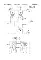
- An alternative current amplifier 24'is shown in FIG. 5.
- a third transistor 60is added in parallel with the other transistors 60.
- the base and the collectorare connected in common with the base in collector of another of the transistors 60.
- a resistor 62connects to the emitter.
- a gain factor of threeis provided by using the same resistor value for all three resistors 62 connected to the emitters of the transistors 60.
- Other current amplifiersmay be used.
- the output of the current amplifier 52is provided to the output stage 54.
- the output stage 54includes two transistors 66, such as 300 volt, 1 amp FET transistors. Other transistors may be used.
- a bias voltagesuch as 35 volts, is applied to each of the transistors 66.
- the output stage 66provides high voltage output swing.
- the output from the output stage 54is provided to the transformer 56.
- the transformer 56includes PW winding 68, output windings 70, and CW windings 72.
- a fixed power supplyconnects to each of the PW winding 68, such as a 210 volt power supply.
- a low power supplyconnects to each of the CW windings 72, such as a fixed 12 volt supply.
- an amplified signalis generated at the output 74.
- a high gain or winding ratiosuch as the three halves or another value, is used for PW operation.
- the current generated at the output 74is a function of the sum of the currents through the PW windings 68 and the CW windings 72.
- only one amplifier stageis operational at any given time, so the current through the output 74 is a function of the current of the operational amplifier stage.
- the voltage at the output 74is capable of varying peak to peak by 160 volts ( ⁇ 80 volts), such as for PW operation.
- the minimum potential gate to drain voltage on transisters 54is preferably 50 or more volts above the bias voltage of the output stage 54.
- the 210 volts of the supply minus the winding ratio (3/2) multiplied by the 80 volts of the output 74is 90 volts.
- 90 voltsis 55 volts higher than the 35 bias voltage.
- the voltage across the CW windingsvaries around the 12 volt supply voltage by the ratio (1/2) of the CW windings 72 to the output winding 70 multiplied by the output voltage.
- the 12 volts plus or minus (1/2) 80is 12 volts plus or minus 40 volts.
- the voltagemay be negative.
- the diodes 58prevent or block the negative voltage from disturbing the gain voltage and the CW current setting transistors 50.
- the effective winding ratio(ratio of CW winding 72 to the output winding 70) is one half, but other winding ratios may be used.
- the one half winding ratioresults in a reduction in current at the output 74.
- a one to one ratiois used.
- the voltage supplyis preferably a 20 volt voltage supply, and the current setting transistors 50 are capable of handling approximately 60 volts.
- the voltagevaries by ⁇ 80 about the 12 volt voltage supply.
- the amplified transmit signal at the output 74(from either the CW or PW amplifier stages) is provided to a transducer element.
- the amplified transmit signalmay be filtered or otherwise processed prior to application to the transducer element.
- the current setting transistors 48 and 50, the diodes 58 and the current amplifier 24are included on an integrated circuit as represented by dashed box 76. Additional or fewer components may be provided on the integrated circuit.
- FIG. 3an alternative embodiment of the amplifier channel is generally shown at 80.
- the CW amplifier stageis not connected to the output 74 through the transformer 56.
- a current amplifier 82is provided for supplying the amplified transmit signal to the output 74.
- the same reference numerals used for FIG. 2are used in FIG. 3.
- FIG. 4a preferred embodiment of the current amplifier 82 is shown.
- the current amplifier 82includes three sets of resistors and transistors 83, 84, 86, a positive 12 volt supply 94, a negative 12 volt supply 92, and two diodes 88 and 90.
- high voltage diodescapable of withstanding a 100 volts in the reverse direction are used.
- the transistors of the sets 84 and 86 connected to the output 74are preferably capable of withstanding the full voltage swing at the output 74 during PW operation.
- the transistors 83are 30 volt and up to 200 miliamp PNP transistors; the transistors 84 are 100 volt, 200 miliamp PNP transistors capable of withstanding 80 volts collector to base; and the transistors 86 are 100 volt, 200 miliamp NPN transistors also capable of withstanding 80 volts collector to base.
- Other transistors with different valuesmay be used.
- the resistorsare 5 to 20 ohms, but other resistors may be used.
- the asymmetrical current mirroring of the current amplifier 82increases the level of even harmonic terms.
- the diode 88allows greater than 12 volt signals to pass to the output 74, and the diode 90 allows less than minus 12 volt signals to pass to the transistor in a set 86.
- the current amplifier 82provides a high impedance. For the differential current representing the rectified positive values, the current is sourced from the 12 volt power supply 94 by the set 84 of transistors. For the negative portions of the differential current, the current is sourced from the 12 volt power supply 94 and sunk from the minus 12 volt power supply 92 through the sets 83 and 86 of transistors. Other current amplification structures may be used.
Landscapes
- Engineering & Computer Science (AREA)
- Computer Networks & Wireless Communication (AREA)
- Physics & Mathematics (AREA)
- General Physics & Mathematics (AREA)
- Radar, Positioning & Navigation (AREA)
- Remote Sensing (AREA)
- Power Engineering (AREA)
- Amplifiers (AREA)
Abstract
Description
Claims (27)
Priority Applications (1)
| Application Number | Priority Date | Filing Date | Title |
|---|---|---|---|
| US09/021,083US6028484A (en) | 1998-02-10 | 1998-02-10 | Ultrasound apparatus and method for amplifying transmit signals |
Applications Claiming Priority (1)
| Application Number | Priority Date | Filing Date | Title |
|---|---|---|---|
| US09/021,083US6028484A (en) | 1998-02-10 | 1998-02-10 | Ultrasound apparatus and method for amplifying transmit signals |
Publications (1)
| Publication Number | Publication Date |
|---|---|
| US6028484Atrue US6028484A (en) | 2000-02-22 |
Family
ID=21802255
Family Applications (1)
| Application Number | Title | Priority Date | Filing Date |
|---|---|---|---|
| US09/021,083Expired - LifetimeUS6028484A (en) | 1998-02-10 | 1998-02-10 | Ultrasound apparatus and method for amplifying transmit signals |
Country Status (1)
| Country | Link |
|---|---|
| US (1) | US6028484A (en) |
Cited By (12)
| Publication number | Priority date | Publication date | Assignee | Title |
|---|---|---|---|---|
| US20030155973A1 (en)* | 2002-02-19 | 2003-08-21 | Hitachi, Ltd. | Variable gain amplifier |
| US20050052200A1 (en)* | 2003-09-08 | 2005-03-10 | Nguyen Huy M. | Calibration methods and circuits for optimized on-die termination |
| US20050134303A1 (en)* | 2003-12-19 | 2005-06-23 | Best Scott C. | Calibration methods and circuits for optimized on-die termination |
| US20050171431A1 (en)* | 2004-01-21 | 2005-08-04 | Siemens Medical Solutions Usa, Inc. | Integrated low-power pw/cw transmitter |
| US20050192499A1 (en)* | 2004-02-26 | 2005-09-01 | Siemens Medical Solutions Usa, Inc. | Subarray forming system and method for ultrasound |
| US20060103463A1 (en)* | 2004-11-16 | 2006-05-18 | Industrial Technology Research Institute | Programmable gain current amplifier |
| US20060132171A1 (en)* | 2004-12-20 | 2006-06-22 | Rambus Inc. | Integrated circuit device with controllable on-die impedance |
| US20070010961A1 (en)* | 2005-07-06 | 2007-01-11 | Rambus Inc. | Driver calibration methods and circuits |
| US20070016049A1 (en)* | 2005-07-15 | 2007-01-18 | Medison Co., Ltd. | Ultrasound diagnostic system and method of forming Tx and Rx beams by using delay data |
| US20070139071A1 (en)* | 2005-12-19 | 2007-06-21 | Rambus Inc. | Configurable on-die termination |
| US20100087737A1 (en)* | 2008-10-02 | 2010-04-08 | Kabushiki Kaisha Toshiba | Ultrasound imaging apparatus and method for generating ultrasound image |
| CN109564278A (en)* | 2016-08-04 | 2019-04-02 | 皇家飞利浦有限公司 | Front-end circuit of ultrasound system for 128-element array probe |
Citations (5)
| Publication number | Priority date | Publication date | Assignee | Title |
|---|---|---|---|---|
| US4593251A (en)* | 1981-06-29 | 1986-06-03 | Smith Randall C | Power amplifier capable of simultaneous operation in two classes |
| US5438684A (en)* | 1992-03-13 | 1995-08-01 | Motorola, Inc. | Radio frequency signal power amplifier combining network |
| US5548246A (en)* | 1994-06-09 | 1996-08-20 | Mitsubishi Denki Kabushiki Kaisha | Power amplifier including an impedance matching circuit and a switch FET |
| US5675554A (en)* | 1994-08-05 | 1997-10-07 | Acuson Corporation | Method and apparatus for transmit beamformer |
| US5694937A (en)* | 1995-01-31 | 1997-12-09 | Kabushiki Kaisha Toshiba | Ultrasound diagnostic apparatus and method |
- 1998
- 1998-02-10USUS09/021,083patent/US6028484A/ennot_activeExpired - Lifetime
Patent Citations (5)
| Publication number | Priority date | Publication date | Assignee | Title |
|---|---|---|---|---|
| US4593251A (en)* | 1981-06-29 | 1986-06-03 | Smith Randall C | Power amplifier capable of simultaneous operation in two classes |
| US5438684A (en)* | 1992-03-13 | 1995-08-01 | Motorola, Inc. | Radio frequency signal power amplifier combining network |
| US5548246A (en)* | 1994-06-09 | 1996-08-20 | Mitsubishi Denki Kabushiki Kaisha | Power amplifier including an impedance matching circuit and a switch FET |
| US5675554A (en)* | 1994-08-05 | 1997-10-07 | Acuson Corporation | Method and apparatus for transmit beamformer |
| US5694937A (en)* | 1995-01-31 | 1997-12-09 | Kabushiki Kaisha Toshiba | Ultrasound diagnostic apparatus and method |
Cited By (64)
| Publication number | Priority date | Publication date | Assignee | Title |
|---|---|---|---|---|
| US20030155973A1 (en)* | 2002-02-19 | 2003-08-21 | Hitachi, Ltd. | Variable gain amplifier |
| US6734730B2 (en)* | 2002-02-19 | 2004-05-11 | Hitachi, Ltd. | Variable gain amplifier |
| US7564258B2 (en) | 2003-09-08 | 2009-07-21 | Rambus Inc. | Calibration methods and circuits to calibrate drive current and termination impedance |
| US10270441B2 (en) | 2003-09-08 | 2019-04-23 | Rambus Inc. | Calibration methods and circuits to calibrate drive current and termination impedance |
| US6924660B2 (en) | 2003-09-08 | 2005-08-02 | Rambus Inc. | Calibration methods and circuits for optimized on-die termination |
| US8278968B2 (en) | 2003-09-08 | 2012-10-02 | Rambus Inc. | Calibration methods and circuits to calibrate drive current and termination impedance |
| US20050174143A1 (en)* | 2003-09-08 | 2005-08-11 | Nguyen Huy M. | Calibration methods and circuits for optimized on-die termination |
| US7928757B2 (en) | 2003-09-08 | 2011-04-19 | Rambus Inc. | Calibration methods and circuits to calibrate drive current and termination impedance |
| US20100259295A1 (en)* | 2003-09-08 | 2010-10-14 | Rambus Inc. | Calibration Methods and Circuits to Calibrate Drive Current and Termination Impedance |
| US9191243B2 (en) | 2003-09-08 | 2015-11-17 | Rambus Inc. | Calibration methods and circuits to calibrate drive current and termination impedance |
| US7741868B2 (en) | 2003-09-08 | 2010-06-22 | Rambus Inc. | Calibration methods and circuits to calibrate drive current and termination impedance |
| US9391613B2 (en) | 2003-09-08 | 2016-07-12 | Rambus Inc. | Calibration methods and circuits to calibrate drive current and termination impedance |
| US20090278565A1 (en)* | 2003-09-08 | 2009-11-12 | Rambus Inc. | Calibration Methods and Circuits to Calibrate Drive Current and Termination Impedance |
| US7151390B2 (en) | 2003-09-08 | 2006-12-19 | Rambus Inc. | Calibration methods and circuits for optimized on-die termination |
| US20110193591A1 (en)* | 2003-09-08 | 2011-08-11 | Rambus Inc. | Calibration Methods and Circuits to Calibrate Drive Current and Termination Impedance |
| US20050052200A1 (en)* | 2003-09-08 | 2005-03-10 | Nguyen Huy M. | Calibration methods and circuits for optimized on-die termination |
| US11522544B2 (en) | 2003-09-08 | 2022-12-06 | Rambus Inc. | Calibration methods and circuits to calibrate drive current and termination impedance |
| US7525338B2 (en) | 2003-09-08 | 2009-04-28 | Rambus Inc. | Calibration methods and circuits for optimized on-die termination |
| US10666254B2 (en) | 2003-09-08 | 2020-05-26 | Rambus Inc. | Calibration methods and circuits to calibrate drive current and termination impedance |
| US9780784B2 (en) | 2003-09-08 | 2017-10-03 | Rambus Inc. | Calibration methods and circuits to calibrate drive current and termination impedance |
| US7408378B2 (en) | 2003-12-19 | 2008-08-05 | Rambus Inc. | Calibration methods and circuits for optimized on-die termination |
| US20050134303A1 (en)* | 2003-12-19 | 2005-06-23 | Best Scott C. | Calibration methods and circuits for optimized on-die termination |
| US6980020B2 (en) | 2003-12-19 | 2005-12-27 | Rambus Inc. | Calibration methods and circuits for optimized on-die termination |
| US20060071683A1 (en)* | 2003-12-19 | 2006-04-06 | Rambus Inc. | Calibration methods and circuits for optimized on-die termination |
| US7588539B2 (en) | 2004-01-21 | 2009-09-15 | Siemens Medical Solutions Usa, Inc. | Integrated low-power pw/cw transmitter |
| US20050171431A1 (en)* | 2004-01-21 | 2005-08-04 | Siemens Medical Solutions Usa, Inc. | Integrated low-power pw/cw transmitter |
| US20050192499A1 (en)* | 2004-02-26 | 2005-09-01 | Siemens Medical Solutions Usa, Inc. | Subarray forming system and method for ultrasound |
| US7517317B2 (en) | 2004-02-26 | 2009-04-14 | Siemens Medical Solutions Usa, Inc. | Subarray forming system and method for ultrasound |
| US7088180B2 (en)* | 2004-11-16 | 2006-08-08 | Industrial Technology Research Institute | Programmable gain current amplifier |
| US20060103463A1 (en)* | 2004-11-16 | 2006-05-18 | Industrial Technology Research Institute | Programmable gain current amplifier |
| US20060132171A1 (en)* | 2004-12-20 | 2006-06-22 | Rambus Inc. | Integrated circuit device with controllable on-die impedance |
| US7196567B2 (en) | 2004-12-20 | 2007-03-27 | Rambus Inc. | Systems and methods for controlling termination resistance values for a plurality of communication channels |
| US7439789B2 (en) | 2004-12-20 | 2008-10-21 | Rambus Inc. | Systems and methods for controlling termination resistance values for a plurality of communication channels |
| US20070159228A1 (en)* | 2004-12-20 | 2007-07-12 | Rambus Inc. | Systems and methods for controlling termination resistance values for a plurality of communication channels |
| US7389194B2 (en) | 2005-07-06 | 2008-06-17 | Rambus Inc. | Driver calibration methods and circuits |
| US20070010961A1 (en)* | 2005-07-06 | 2007-01-11 | Rambus Inc. | Driver calibration methods and circuits |
| US8988100B2 (en) | 2005-07-06 | 2015-03-24 | Rambus Inc. | Driver calibration methods and circuits |
| US20100318311A1 (en)* | 2005-07-06 | 2010-12-16 | Rambus Inc. | Driver Calibration Methods and Circuits |
| US8237468B2 (en) | 2005-07-06 | 2012-08-07 | Rambus Inc. | Driver calibration methods and circuits |
| US20070016049A1 (en)* | 2005-07-15 | 2007-01-18 | Medison Co., Ltd. | Ultrasound diagnostic system and method of forming Tx and Rx beams by using delay data |
| JP2007021214A (en)* | 2005-07-15 | 2007-02-01 | Medison Co Ltd | Ultrasonic diagnostic system forming transmission beam and reception beam using delay data stored in memory and method therefor |
| US10236882B2 (en) | 2005-12-19 | 2019-03-19 | Rambus Inc. | Integrated circuit with configurable on-die termination |
| US20070139071A1 (en)* | 2005-12-19 | 2007-06-21 | Rambus Inc. | Configurable on-die termination |
| US8466709B2 (en) | 2005-12-19 | 2013-06-18 | Rambus Inc. | Integrated circuit with configurable on-die termination |
| US12224748B2 (en) | 2005-12-19 | 2025-02-11 | Rambus Inc. | Integrated circuit with configurable on-die termination |
| US8941407B2 (en) | 2005-12-19 | 2015-01-27 | Rambus Inc. | Integrated circuit with configurable on-die termination |
| US20100237903A1 (en)* | 2005-12-19 | 2010-09-23 | Rambus Inc. | Configurable On-Die Termination |
| US7772876B2 (en) | 2005-12-19 | 2010-08-10 | Rambus Inc. | Configurable on-die termination |
| US11843372B2 (en) | 2005-12-19 | 2023-12-12 | Rambus Inc. | Integrated circuit with configurable on-die termination |
| US8072235B2 (en) | 2005-12-19 | 2011-12-06 | Rambus Inc. | Integrated circuit with configurable on-die termination |
| US9685951B2 (en) | 2005-12-19 | 2017-06-20 | Rambus Inc. | Integrated circuit with configurable on-die termination |
| US7948262B2 (en) | 2005-12-19 | 2011-05-24 | Rambus Inc. | Configurable on-die termination |
| US20110128041A1 (en)* | 2005-12-19 | 2011-06-02 | Rambus Inc. | Integrated Circuit With Configurable On-Die Termination |
| US9338037B2 (en) | 2005-12-19 | 2016-05-10 | Rambus Inc. | Integrated circuit with configurable on-die termination |
| US11012071B2 (en) | 2005-12-19 | 2021-05-18 | Rambus Inc. | Integrated circuit with configurable on-die termination |
| US7439760B2 (en) | 2005-12-19 | 2008-10-21 | Rambus Inc. | Configurable on-die termination |
| US10651848B2 (en) | 2005-12-19 | 2020-05-12 | Rambus Inc. | Integrated circuit with configurable on-die termination |
| US20090051389A1 (en)* | 2005-12-19 | 2009-02-26 | Rambus Inc. | Configurable on-die termination |
| US20100087737A1 (en)* | 2008-10-02 | 2010-04-08 | Kabushiki Kaisha Toshiba | Ultrasound imaging apparatus and method for generating ultrasound image |
| US8491476B2 (en) | 2008-10-02 | 2013-07-23 | Kabushiki Kaisha Toshiba | Ultrasound imaging apparatus and method for generating ultrasound image |
| KR20190035851A (en)* | 2016-08-04 | 2019-04-03 | 코닌클리케 필립스 엔.브이. | Ultrasonic system front-end circuit for 128-element array probes |
| US11442156B2 (en)* | 2016-08-04 | 2022-09-13 | Koninklijke Philips N.V. | Ultrasound system front-end circuit for a 128-element array probe |
| CN109564278A (en)* | 2016-08-04 | 2019-04-02 | 皇家飞利浦有限公司 | Front-end circuit of ultrasound system for 128-element array probe |
| CN109564278B (en)* | 2016-08-04 | 2024-03-19 | 皇家飞利浦有限公司 | Ultrasound system front-end circuit for 128-element array probe |
Similar Documents
| Publication | Publication Date | Title |
|---|---|---|
| US6028484A (en) | Ultrasound apparatus and method for amplifying transmit signals | |
| US6808494B2 (en) | Transmit circuit for imaging with ultrasound | |
| US4801823A (en) | Sample hold circuit | |
| US4580111A (en) | Amplitude modulation using digitally selected carrier amplifiers | |
| US6537216B1 (en) | Transmit circuit for imaging with ultrasound | |
| EP1971025B1 (en) | Digital input class-D amplifier | |
| RU2160497C2 (en) | Method and device for digital-to-analog conversion | |
| US20040201418A1 (en) | Power supply processing for power amplifiers | |
| US5619203A (en) | Current source driven converter | |
| US6563376B2 (en) | Mute circuit and digital audio amplifier circuit | |
| KR100431256B1 (en) | Digital-to-analog converter | |
| US4390849A (en) | Audio power amplifier with class-D push-pull output stage | |
| US11349441B2 (en) | Method and apparatus of adaptive gate bias for switched driver | |
| US6690236B2 (en) | Gain variable amplifier | |
| JPS54152846A (en) | Pulse duration modulating signal amplifier circuit | |
| KR930020859A (en) | Analog digital converter | |
| US5861830A (en) | Digital to analog converter and dynamic current mirror structure to simplify on-chip wave shaping | |
| JPS5916443B2 (en) | power amplifier | |
| JPH0621814A (en) | Digital-to-analog converter provided with precise linear output for both positive and negative input values | |
| KR100417744B1 (en) | Amplitude adjustment circuit and amplitude adjustment method | |
| US6522273B1 (en) | Circuits systems and methods for power digital-to-analog converter protection | |
| JPH031709A (en) | Variable resistance circuit and variable gain amplifier | |
| JPH0520007Y2 (en) | ||
| JPH0115218Y2 (en) | ||
| US6992607B2 (en) | Speech synthesizer |
Legal Events
| Date | Code | Title | Description |
|---|---|---|---|
| AS | Assignment | Owner name:ACUSON CORPORATION, CALIFORNIA Free format text:ASSIGNMENT OF ASSIGNORS INTEREST;ASSIGNORS:COLE, CHRISTOPHER R.;NEWELL, LAURENCE J.;REEL/FRAME:008976/0452;SIGNING DATES FROM 19980203 TO 19980204 | |
| STCF | Information on status: patent grant | Free format text:PATENTED CASE | |
| FPAY | Fee payment | Year of fee payment:4 | |
| FPAY | Fee payment | Year of fee payment:8 | |
| AS | Assignment | Owner name:SIEMENS MEDICAL SOLUTIONS USA, INC.,PENNSYLVANIA Free format text:CHANGE OF NAME;ASSIGNOR:SIEMENS MEDICAL SYSTEMS, INC.;REEL/FRAME:024563/0051 Effective date:20010801 | |
| AS | Assignment | Owner name:SIEMENS MEDICAL SOLUTIONS USA, INC., PENNSYLVANIA Free format text:RE-RECORD TO CORRECT CONVEYING PARTY NAME PREVIOUSLY RECORDED AT REEL 024563 FRAME 0051;ASSIGNORS:ACUSON CORPORATION;ACUSON LLC;ACUSON CORPORATION;SIGNING DATES FROM 20021218 TO 20050926;REEL/FRAME:024651/0673 | |
| FPAY | Fee payment | Year of fee payment:12 |