US6027760A - Photoresist coating process control with solvent vapor sensor - Google Patents
Photoresist coating process control with solvent vapor sensorDownload PDFInfo
- Publication number
- US6027760A US6027760AUS08/987,179US98717997AUS6027760AUS 6027760 AUS6027760 AUS 6027760AUS 98717997 AUS98717997 AUS 98717997AUS 6027760 AUS6027760 AUS 6027760A
- Authority
- US
- United States
- Prior art keywords
- solvent
- solvent vapor
- carrier gas
- concentration
- spin coating
- Prior art date
- Legal status (The legal status is an assumption and is not a legal conclusion. Google has not performed a legal analysis and makes no representation as to the accuracy of the status listed.)
- Expired - Lifetime
Links
- 239000002904solventSubstances0.000titleclaimsabstractdescription275
- 238000000576coating methodMethods0.000titleclaimsabstractdescription43
- 229920002120photoresistant polymerPolymers0.000titledescription18
- 239000012159carrier gasSubstances0.000claimsabstractdescription86
- 239000007789gasSubstances0.000claimsabstractdescription68
- 229920000642polymerPolymers0.000claimsabstractdescription43
- 238000004528spin coatingMethods0.000claimsabstractdescription38
- 239000011248coating agentSubstances0.000claimsabstractdescription37
- 239000007788liquidSubstances0.000claimsabstractdescription26
- 230000003287optical effectEffects0.000claimsabstractdescription22
- 239000012528membraneSubstances0.000claimsabstractdescription10
- 238000002156mixingMethods0.000claimsabstractdescription3
- 238000000034methodMethods0.000claimsdescription31
- 230000008859changeEffects0.000claimsdescription8
- 230000010287polarizationEffects0.000claimsdescription5
- 230000004044responseEffects0.000claimsdescription5
- 230000003595spectral effectEffects0.000claimsdescription4
- 238000002347injectionMethods0.000abstract1
- 239000007924injectionSubstances0.000abstract1
- 230000008569processEffects0.000description18
- 229920006395saturated elastomerPolymers0.000description12
- 238000012545processingMethods0.000description9
- 239000004065semiconductorSubstances0.000description9
- 239000000203mixtureSubstances0.000description8
- 230000005855radiationEffects0.000description7
- 229920001730Moisture cure polyurethanePolymers0.000description6
- 239000000463materialSubstances0.000description5
- 239000000758substrateSubstances0.000description5
- 238000001816coolingMethods0.000description4
- 238000010438heat treatmentMethods0.000description4
- 238000004519manufacturing processMethods0.000description4
- 238000001704evaporationMethods0.000description3
- 230000008020evaporationEffects0.000description3
- 229920006254polymer filmPolymers0.000description3
- 239000007921spraySubstances0.000description3
- CSCPPACGZOOCGX-UHFFFAOYSA-NAcetoneChemical compoundCC(C)=OCSCPPACGZOOCGX-UHFFFAOYSA-N0.000description2
- 230000001419dependent effectEffects0.000description2
- 238000005530etchingMethods0.000description2
- LZCLXQDLBQLTDK-UHFFFAOYSA-Nethyl 2-hydroxypropanoateChemical compoundCCOC(=O)C(C)OLZCLXQDLBQLTDK-UHFFFAOYSA-N0.000description2
- 238000005259measurementMethods0.000description2
- LLHKCFNBLRBOGN-UHFFFAOYSA-Npropylene glycol methyl ether acetateChemical compoundCOCC(C)OC(C)=OLLHKCFNBLRBOGN-UHFFFAOYSA-N0.000description2
- 238000000935solvent evaporationMethods0.000description2
- 238000009987spinningMethods0.000description2
- 239000000126substanceSubstances0.000description2
- 238000012546transferMethods0.000description2
- IJGRMHOSHXDMSA-UHFFFAOYSA-NAtomic nitrogenChemical compoundN#NIJGRMHOSHXDMSA-UHFFFAOYSA-N0.000description1
- 230000002745absorbentEffects0.000description1
- 239000002250absorbentSubstances0.000description1
- 238000010521absorption reactionMethods0.000description1
- 230000009471actionEffects0.000description1
- 230000003044adaptive effectEffects0.000description1
- 229910001873dinitrogenInorganic materials0.000description1
- 238000009826distributionMethods0.000description1
- 238000010894electron beam technologyMethods0.000description1
- 230000007613environmental effectEffects0.000description1
- 229940116333ethyl lactateDrugs0.000description1
- 230000002401inhibitory effectEffects0.000description1
- 238000010884ion-beam techniqueMethods0.000description1
- 230000001404mediated effectEffects0.000description1
- 238000012544monitoring processMethods0.000description1
- 229920000620organic polymerPolymers0.000description1
- 239000003960organic solventSubstances0.000description1
- 230000037361pathwayEffects0.000description1
- 238000000206photolithographyMethods0.000description1
- 239000005373porous glassSubstances0.000description1
- 238000004886process controlMethods0.000description1
- 238000010926purgeMethods0.000description1
- 230000035945sensitivityEffects0.000description1
- 238000003892spreadingMethods0.000description1
- 230000007480spreadingEffects0.000description1
- 238000010561standard procedureMethods0.000description1
Images


Classifications
- B—PERFORMING OPERATIONS; TRANSPORTING
- B05—SPRAYING OR ATOMISING IN GENERAL; APPLYING FLUENT MATERIALS TO SURFACES, IN GENERAL
- B05D—PROCESSES FOR APPLYING FLUENT MATERIALS TO SURFACES, IN GENERAL
- B05D1/00—Processes for applying liquids or other fluent materials
- B05D1/002—Processes for applying liquids or other fluent materials the substrate being rotated
- B05D1/005—Spin coating
- B—PERFORMING OPERATIONS; TRANSPORTING
- B05—SPRAYING OR ATOMISING IN GENERAL; APPLYING FLUENT MATERIALS TO SURFACES, IN GENERAL
- B05C—APPARATUS FOR APPLYING FLUENT MATERIALS TO SURFACES, IN GENERAL
- B05C11/00—Component parts, details or accessories not specifically provided for in groups B05C1/00 - B05C9/00
- B05C11/02—Apparatus for spreading or distributing liquids or other fluent materials already applied to a surface ; Controlling means therefor; Control of the thickness of a coating by spreading or distributing liquids or other fluent materials already applied to the coated surface
- B05C11/08—Spreading liquid or other fluent material by manipulating the work, e.g. tilting
- G—PHYSICS
- G03—PHOTOGRAPHY; CINEMATOGRAPHY; ANALOGOUS TECHNIQUES USING WAVES OTHER THAN OPTICAL WAVES; ELECTROGRAPHY; HOLOGRAPHY
- G03F—PHOTOMECHANICAL PRODUCTION OF TEXTURED OR PATTERNED SURFACES, e.g. FOR PRINTING, FOR PROCESSING OF SEMICONDUCTOR DEVICES; MATERIALS THEREFOR; ORIGINALS THEREFOR; APPARATUS SPECIALLY ADAPTED THEREFOR
- G03F7/00—Photomechanical, e.g. photolithographic, production of textured or patterned surfaces, e.g. printing surfaces; Materials therefor, e.g. comprising photoresists; Apparatus specially adapted therefor
- G03F7/16—Coating processes; Apparatus therefor
- G03F7/162—Coating on a rotating support, e.g. using a whirler or a spinner
- B—PERFORMING OPERATIONS; TRANSPORTING
- B05—SPRAYING OR ATOMISING IN GENERAL; APPLYING FLUENT MATERIALS TO SURFACES, IN GENERAL
- B05D—PROCESSES FOR APPLYING FLUENT MATERIALS TO SURFACES, IN GENERAL
- B05D3/00—Pretreatment of surfaces to which liquids or other fluent materials are to be applied; After-treatment of applied coatings, e.g. intermediate treating of an applied coating preparatory to subsequent applications of liquids or other fluent materials
- B05D3/04—Pretreatment of surfaces to which liquids or other fluent materials are to be applied; After-treatment of applied coatings, e.g. intermediate treating of an applied coating preparatory to subsequent applications of liquids or other fluent materials by exposure to gases
- B05D3/0486—Operating the coating or treatment in a controlled atmosphere
Definitions
- This inventionrelates to coating semiconductor substrates with organic photoresist polymers.
- this inventionrelates to an improved apparatus and process for coating semiconductor substrates with solutions of organic polymers in the presence of volatile solvents, with improved control of volatile solvent emissions from the coating.
- the manufacture of integrated circuitsinvolves the transfer of geometric shapes on a mask to the surface of a semiconductor wafer. Thereafter, the semiconductor wafer corresponding to the geometric shapes, or corresponding to the areas between the geometric shapes, is etched away.
- the transfer of the shapes from the mask to the semiconductor wafertypically involves a lithographic process. This includes applying a solution of a pre-polymer solution to the semiconductor wafer, the pre-polymer being selected to form a radiation-sensitive polymer which reacts when exposed to ultraviolet light, electron beams, x-rays, or ion beams, for example.
- the solvent in the pre-polymer solutionis removed by evaporation, and the resulting polymer film is then baked.
- the filmis exposed to radiation, for example, ultraviolet light, through a photomask supporting the desired geometric patterns.
- the images in the photosensitive materialare then developed by soaking the wafer in a developing solution.
- the exposed or unexposed areasare removed in the developing process, depending on the nature of the radiation-sensitive material.
- the waferis placed in an etching environment which etches away the areas not protected by the radiation-sensitive material. Due to their resistance to the etching process, the radiation sensitive-materials are also known as photoresists, and the term photoresist is used hereinafter to denote the radiation-sensitive polymers and their pre-polymers.
- the high cost of the photoresist pre-polymer solutionsmakes it desirable to devise methods of improving the efficiency of the coating process so as to minimize the amount of the polymer solution required to coat a substrate.
- thickness uniformity of the photoresist layeris an important criterion in the manufacture of integrated circuits.
- variations in thickness of the coatingprevent the precise focus over the entire surface of the wafer which is required to obtain the sharpness necessary to ensure satisfactory reproduction of the geometric patterns on the semiconductor wafer for advanced circuits with line width dimensions approaching 0.25 micron line widths and smaller over a surface.
- the solvent in the photoresisttends to evaporate during application, increasing the viscosity of the polymer solution and inhibiting the leveling of the resulting film. This produces thickness non-uniformities. It is therefore desirable to be able to control the rate of evaporation of solvent from the polymer solution during the coating process.
- One object of this inventionis to provide an improved wafer coating process which yields a greater coating uniformity across the entire surface of each wafer and from wafer-to-wafer.
- Another object of this inventionis to provide more accurate control of the solvent vapor concentration above the surface of a wafer during the coating and solvent removal phases of the coating process.
- an apparatus of this invention for spin coating surfaces with liquid polymercomprises a spin coating chamber having a rotatable chuck for supporting an object to be coated.
- a distributorcommunicates with the coating chamber and is positioned to introduce gases into the chamber.
- a solvent vapor and carrier gas supply control meanscommunicates with the distributor.
- the solvent vapor and carrier gas supplyprovides a carrier gas having a controlled level of solvent vapor therein within the range of from 0 to saturation concentrations of solvent vapor.
- a solvent vapor sensoris positioned within the coating chamber to produce signals which are a function of the concentration of solvent vapor in the coating chamber.
- the control meansis connected to the solvent vapor concentration sensor and to the solvent vapor and carrier gas supply means for controlling the level of solvent vapor in the carrier gas supplied by the solvent vapor and carrier gas supply means.
- the apparatusincludes a coating zone adjacent the rotatable chuck corresponding to the surface to be coated, and the solvent vapor sensor is positioned between the distributor and the coating zone.
- the solvent vapor and carrier gas supply meanscan comprise a solvent vapor supply conduit communicating with the distributor, a carrier gas supply conduit communicating with the distributor, and control valve means positioned with respect to the solvent vapor supply conduit and the carrier gas supply conduit for the purpose of controlling the proportion of gases from the conduits which are supplied to the distributor.
- the solvent vapor and carrier gas supply meanscan include a gas supply manifold communicating with the distributor and with the solvent vapor supply conduit and the carrier gas supply conduit, wherein the control valve means is positioned with respect to the manifold, the solvent vapor supply conduit and the carrier gas supply conduit for controlling the proportion of gases from the conduits which are supplied to the distributor.
- the manifoldcan have an inlet, the solvent vapor supply conduit and carrier gas supply conduit can have outlets, and the control valve means can be a valve positioned to simultaneously control flow from each of the outlets.
- the solvent vapor supply conduit and the carrier gas supply conduitcan each have control valves which are positioned to control flow from the conduits to the distributor.
- the solvent vapor and carrier gas supply meansincludes a distributor manifold, a carrier gas supply conduit communicates with the manifold, and a solvent atomizer with a solvent atomizer pump communicates with the manifold.
- the control meansis connected to the solvent vapor concentration sensor and to the solvent atomizer pump to control the amount of solvent to be atomized by the atomizer into the manifold.
- the solvent vapor and carrier gas supply meansincludes a carrier gas supply conduit communicating with the distributor, and a solvent atomizer with a solvent atomizer pump communicating with the carrier gas conduit.
- the control meansis connected to the solvent vapor concentration sensor and to the solvent atomizer pump for controlling the amount of solvent to be atomized by the atomizer into the carrier gas supply conduit.
- the solvent vapor concentration sensorcan include a component positioned for exposure to solvent vapor and which has a property which changes as a function of the solvent vapor concentration to which it is exposed.
- the sensorcan include a membrane, the vibrational frequency of which changes as a function of the solvent vapor concentration to which it is exposed; it can include a surface, the electrical properties of which change as a function of the solvent vapor concentration to which it is exposed; or it can detect an acoustical property which is a function of the solvent vapor concentration.
- the sensorcan include an optical detector optically exposed to the solvent vapor, the optical detector sensing an optical property of the solvent which is a function of the solvent vapor concentration.
- the optical detectorcan include a spectrophotometer which measures a spectral property of the solvent vapor, such as polarization shift properties, which changes as a function of the solvent vapor concentration.
- the method of this invention for spin coating a surface with a polymer in a volatile solvent environmentcomprises applying the polymer to a surface to be coated in a coating chamber, passing a carrier gas through the coating chamber, the carrier gas having a concentration of volatile solvent for the liquid polymer therein, generating a signal which is a function of the concentration of volatile solvent in the carrier gas by means of a solvent vapor concentration sensor positioned near the surface being coated with the polymer, while carrier gas passes through the chamber, and adding an amount of volatile solvent to the carrier gas in response to the signal to produce a desired concentration of volatile solvent in the control gas passing through the chamber.
- the volatile solventcan be added to the carrier gas by mixing together a first gas stream of solvent-free carrier gas and a second gas stream containing solvent vapor at a controlled concentration, the first and second gas streams being mixed in the proportion required to yield a carrier gas having a controlled concentration of solvent vapor therein.
- a controlled amount of solventcan be atomized in the carrier gas to yield a carrier gas having a controlled concentration of solvent vapor therein.
- the solvent vapor concentration sensor positioned in the carrier gas passing through the chambercan include a sensor component positioned for exposure to solvent vapor which has a property which changes as a function of the solvent vapor concentration to which it is exposed.
- the sensorcan be any sensor capable of providing this function.
- Preferred sensorsinclude an acoustic sensor which changes resonant frequency with solvent concentration and produces a signal proportional to solvent concentration.
- the sensorcan include a membrane, the vibrational frequency of which changes as a function of the solvent vapor concentration to which it is exposed; it can include a surface, the electrical properties of which change as a function of the solvent vapor concentration to which it is exposed; or it can detect an acoustical property which is a function of the solvent vapor concentration.
- the sensorcan include an optical detector optically exposed to the solvent vapor, the optical detector sensing an optical property of the solvent which is a function of the solvent vapor concentration.
- the optical detectorcan include a spectrophotometer which measures a spectral property of the solvent vapor, such as polarization shift properties, which changes as a function of the solvent vapor concentration.
- FIG. 1is a schematic view of a spin coating apparatus and a solvent vapor feedback control system associated therewith.
- FIG. 2is a schematic drawing of the solvent vapor concentration control system of this invention.
- FIG. 3is a schematic drawing of an alternative gas flow control valve assembly.
- FIG. 4is a schematic drawing of an atomizer spray solvent system for providing a controlled solvent vapor concentration in carrier gas flowing to the coating chamber.
- the dynamics of viscosity controlare affected by the volatile exchange between the photoresist layer and the surrounding atmosphere during the spin-coating process, that is, solvent molecules in the film continue to leave and solvent molecules in the atmosphere are continuously absorbed by the film.
- some commercial photoresistsmay contain more than one solvent species, each with its own different vapor pressure profile.
- the present inventioncombines with the gas stream mixture a sensor and feedback system to measure the solvent vapor concentration over the wafer surface and to provide adjustment to the incoming solvent vapor concentration to achieve the desired solvent vapor concentration, the feedback circuit controlling the ratio of solvent-saturated gas and solvent-free gas to provide to the wafer surface the precise solvent vapor concentration required by the predictive model. This gives a far higher level of precision to the control of the solvent vapor at the wafer surface.
- FIG. 1is a schematic view of a spin coating apparatus and a solvent vapor feedback control system associated therewith.
- the apparatus 2includes a rotatable support chuck 4 mounted in a spin coating housing 6 and supporting a wafer 5.
- the chuck 4is mounted on an axle 8 which passes through an opening 10 in the housing 6.
- the housing 6includes solvent vapor and carrier gas supply manifold and dispenser 12.
- Dispenser 12introduces a control gas comprising a mixture of a non-solvent gas and a certain concentration of solvent to be passed into the housing 6 above the wafer 5.
- Gasesare fed into the manifold 12 from gas and solvent supply conduit 14 communicating therewith.
- a solvent-free gaswhich is dry, such as air or nitrogen gas, is fed by solvent-free gas conduit 16.
- a carrier gas supply conduit 18 with flow control valve 20communicates with bubbler 26 immersed in a volume of solvent 28 in bubbler chamber 24.
- a solvent vapor saturated gas streamis prepared by passing gas from gas supply conduit 18 through inlet control valve 20 with valve controller 22 to bubbler chamber 24 with bubbler 26, from which the gases pass upward through solvent 28, emerging as solvent-saturated gas at the temperature set for the solvent.
- the bubbler 26 in this embodimentcan be a porous glass frit from which the gas is passed through the liquid solvent 28.
- Outlet conduit 30communicates with the bubbler chamber 24 for receipt of solvent-saturated gas. The gases, saturated with solvent vapor, are removed from chamber 24 through conduit 30.
- Chamber 24has a solvent vapor sensor 32 which generates a signal corresponding to the solvent concentration in the vapor.
- Bubbler chamber 24is surrounded by a temperature control jacket 34 which contains heating/cooling coils 36 or similar conventional means for maintaining or changing the temperature of the solvent 28 at or to a set point.
- the gas supply conduit 18has an optional heater or heat exchanger 37 which controls the temperature of the incoming gas to a set temperature.
- the flows of solvent-free gas stream from conduit 16 and solvent-saturated gas from conduit 30are controlled by the solvent-free gas stream control valve 38 and solvent-saturated gas control valve 40.
- Valves 38 and 40can be any standard, conventional remote control valve, such as mass flow controllers, for example.
- the respective passageways 16 and 30can independently be varied from a totally closed position (such as shown for valve 38) to a completely open position (such as shown for valve 40).
- the gas stream fed to manifold 12can vary from a stream which is completely free from solvent supplied from conduit 16 with valve 38 open and valve 40 closed, to a stream which is saturated with solvent vapor supplied from conduit 30 with valve 38 closed and valve 40 open.
- the valves 38 and 40can be opened to any combination of positions to provide a full range of solvent vapor concentrations from 0 percent solvent to fully saturated solvent vapor in the carrier gas stream.
- the temperature of the solvent-bearing gas supplied by the bubbler 26is maintained or controlled to a set point by heating/cooling coils 36 which control the temperature of the solution 28.
- the temperature of the incoming gas supplied by conduit 18can be raised or lowered or controlled by a heater or heat exchanger 37. Heat must be supplied to the solvent 28 to compensate for heat loss due to evaporation.
- Sensor 32Sensor 32, sensor signal processing and control output generator 42, and temperature controller 44 are connected as described hereinafter with regard to FIG. 2.
- Sensor 32sends signals to a sensor signal processing and control output generator 42 which, in turn, sends control signals to the temperature controller 44 for controlling the energy or liquid supplied to the heating/cooling coils 36 to change or maintain the temperature of the vessel 24 and the liquid contents 28 to a set temperature point.
- the apparatusincludes a dispensing head 46 for applying a solution of photoresist pre-polymer to the upper surface of wafer 5.
- the conventional dispensing head 46can supply a stream of photoresist solution to the center of the wafer 5 or along a surface from the center to the edge, the rotation of the chuck 4 and the wafer 5 spreading the photoresist over the entire wafer surface by centrifugal action, and spinning off the outer edge any excess photoresist solution.
- the gas stream 48 containing the solvent vaporpasses in a stream downward and across the upper surface of wafer 5 to control the atmosphere above the wafer surface and thereby control the rate of solvent evaporation from the photoresist coating.
- the gas flowis quickly drawn over the edge of the wafer, into annular channel 50 and to the exhaust conduit 52 with conventional exhaust valve 54.
- the exhaust control valve 54is connected to a valve controller which is connected to the sensor signal processing and control output generator 64, connected thereto as described with respect to FIG. 2.
- the bottom of the annular channel 50defines an annular drain channel 58 leading to the photoresist drain conduit 60.
- One or more solvent concentration sensors 62are positioned to determine the solvent concentration in the coating chamber. A preferred sensor position is just above the surface of wafer 5, as shown, but sensors 62 can be optionally positioned in the gas stream 48 leading to and leaving the wafer surface.
- the sensors 62are connected to a controller 64, as described in FIG. 2.
- the controller 64is connected to valve mass flow controller (MFC) 66 which connects to valves 38 and 40, the connections being shown in greater detail in FIG. 2.
- MFCvalve mass flow controller
- the semiconductor wafer 5is secured to the chuck 4 using any standard method, such as a vacuum established between the chuck 4 and the wafer 5.
- a wafer transport door (not shown) to the housing 6is thereafter closed.
- the housing 6is purged with dry solvent-free gas from conduit 16 to purge the chamber.
- Control gas having a predetermined concentration of solvent vaporis formed by adjustment of valves 38 and 40 to establish the proper ratio of gases from conduits 16 and 30. If complete solvent saturation is desired, for example, valve 38 might be closed and valve 40 opened to introduce a stream of solvent-saturated gas from the conduit 30.
- the solvent concentration of the control gasis measured by sensor 62, and adjustments are made to the valves 38 and 40 as required to change or maintain a set level of solvent in the incoming gas stream 48 in a continuous feedback system using the sensor signal processing and control output generator 64 and the mass flow controller 66.
- the level of solvent in the carrier gasis adjusted by raising or lowering the temperature of the solvent 28, and optionally, the incoming gas stream from conduit 18 to a temperature level which yields the desired percentage of solvent at full saturation at that temperature.
- the solvent concentrationis measured by sensor 32, and the signal therefrom is used to adjust the temperature of the solution 28, and/or incoming gas from conduit 18, by operation of the sensor signal processing and control output generator 42, temperature controller 44 and carrier gas supply valve controller 22 connected thereto.
- the polymer solutionis applied across the surface of the wafer 5 via the dispensing head 46. This is achieved by dispensing the polymer solution in a continuous stream from a nozzle or similar dispenser (not shown) onto the wafer surface while the wafer 5 is spinning at relatively low speed.
- the nozzleis moved substantially radially across the wafer 5.
- the solutioncan be dispensed at the center of the substrate, or multiple nozzles can be used. By adjusting the spin speed of the wafer 5, the movement of the nozzle, and the rate at which the polymer solution is dispensed, a suitable distribution of the solution can be achieved.
- the polymer solutionis deposited onto the wafer by means of a film extruder.
- the solvent vapor sensors 32 and 62can be any sensor which is capable of generating a signal having a functional relationship to the percentage of solvent in a carrier gas.
- One type of suitable chemical vapor sensoris the resonance sensing microelectromechanical system with a solvent absorbent membrane or plate, the resonance frequency of the membrane being a function of the solvent vapor concentration in the vapor.
- An example of this type of sensoris the Model BMC200 from Berkeley MicroInstruments, Inc. (Richmond, Calif.).
- the electronic unitpowers the sensor and transmits sensor data to the central controller.
- Another example of a sensor suitable for use in the present inventionis the membrane system described in U.S. Pat. No. 5,485,750, the entire contents of which are hereby incorporated by reference.
- vapor concentration sensorsmeasure the solvent concentration by sensing or measuring electrical (e.g., conductivity, impedance (resistance, capacitance), electrochemical, photoconductivity), optical (e.g., absorption, polarization shift), sound (acoustical) and ultrasonic properties of the gas containing the solvent vapor using conventional, well-known devices for these measurements. Sensors using changes in electrical properties in response to exposure of materials to the solvent vapor are described in U.S. Pat. Nos.
- FIG. 2is a schematic drawing of the solvent vapor concentration control system of this invention.
- the sensor signal processing and control output generator 64is the hub of the solvent delivery control system.
- the generator 64has an input, which is connected to the sensors 62 for receipt of information about the solvent vapor concentration in the coating chamber, and outputs connected to valve controllers 22, 56 and 66 for control of valve 20, which controls the flow of carrier gas to the solvent saturator 24 (controller 22); control of valves 38 and 40, which produce the mix of streams of solvent-free carrier gas and carrier gas (controller 66); and control of the exhaust valve 54 (controller 56), which controls the flow of gases exhausted from the coating assembly.
- the hub of the solvent saturator controlsis the sensor signal processing and control output generator 42, having an input which is connected to sensor 42 for receipt of signals denoting the solvent concentration in the vapor above the liquid in the tank, and outputs to temperature controller 44 for the heating/cooling coils controlling the temperature of solvent vessel 24 and heat exchanger 37.
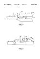
- FIG. 3is a schematic drawing of an alternative gas flow control valve assembly.
- the solvent-free carrier gas supply conduit 68 and the solvent vapor-saturated gas conduit 70merge to form a single solvent vapor-containing gas supply conduit 72 which communicates with a manifold and dispenser, such as the manifold and dispenser 12 shown in FIG. 1.
- a pivotal valve 74pivots on hinge 76, located at the junction of conduits 68 and 70, to rotate about its hinge 76 from a position closing the conduit 68 to a position closing the conduit 70 (shown by dotted line), or to intermediate positions therebetween to partially close one or the other of gas supply conduits 68 and 70.
- the position of valve 74determines the proportion of the solvent-bearing gas supplied to the gas distributor.
- Valve controller 78connects to a step motor or other conventional control system for positioning valve 74.
- Valve controller 78is connected by line 79 to the central sensor signal processing and control output generator, such as the generator 64 shown in FIG. 1.
- FIG. 4is a schematic drawing of an atomizer spray solvent system for providing a controlled solvent vapor concentration in carrier gas flowing to the coating chamber.
- a distributorsuch as the distributor 12 shown in FIG. 1
- Atomizer injector 82which is mounted in the wall of conduit 80, has an outlet communicating with the interior of conduit 80 to introduce a controlled amount or volume of atomized spray of solvent 84 into the carrier gas flowing through the conduit 80.
- the atomizer 82is connected by pressurized gas supply conduit 86 with a supply of gas under pressure, which can be a carrier gas for operation of the aspirator.
- the injector 82is supplied with liquid solvent by solvent pump 88, connected thereto through adjustable needle valve 90, the pump communicating with a solvent reservoir through solvent supply conduit 92.
- the pump and injectorcan be any conventional atomizer and high accuracy flow-controlled pump which are capable of effectively delivering an accurate, controlled flow of solvent into the carrier gas stream.
- Pump controller 94is connected to the pump 88 and, by line 96, with the sensor signal processing and control output generator, such as generator 64 shown in FIG. 1.
- the atomizer 82is controlled by an output generator to provide a controlled volume of solvent into the carrier gas stream in response to the solvent vapor concentration sensed in the coating chamber, as described above, the principal difference with the embodiments described hereinabove being in the system used to create the solvent and carrier gas mixture.
- Optional turbulence mixer 98 in conduit 80disperses the solvent vapors throughout the carrier gas flowing therethrough.
- This inventionprovides an adaptive control of solvent concentration with the process chamber used for spin coating of polymers such as photoresist in the area of photolithography.
- the inventionprovides an improved mean thickness and uniformity control for polymer film processes employed during the manufacture of small feature size advanced devices.
- This inventionuses one or more solvent vapor sensors to measure solvent concentration.
- the output of the sensorsis used to control mass flow controllers in real time by way of an algorithm.
- Sensorsare placed in the process chamber, solvent canister, and/or optionally, in any pathway therebetween. Any fluctuation in solvent temperature or headroom space which may cause variation of the solvent concentration inside the process chamber can be compensated by mass flow controllers in a closed loop fashion to ensure constant and repeatable solvent atmospheres for every wafer processed. Decision-making is done by a process control algorithm which uses known chemical properties of the solvent, required process conditions and numerical models.
- This inventioncan reduce dependence on precise temperature controls for the solvent to achieve the desired solvent concentration in the coating chamber.
- the inventioncan be applied to different systems for introducing the solvent vapor, such as the bubbler system disclosed or a liquid mass flow controller combined with an atomizer, which is also considered to be within the scope of this invention.
- This inventionmakes solvent concentration control within a process chamber totally transparent to the user.
Landscapes
- Physics & Mathematics (AREA)
- General Physics & Mathematics (AREA)
- Coating Apparatus (AREA)
- Exposure Of Semiconductors, Excluding Electron Or Ion Beam Exposure (AREA)
- Investigating Or Analyzing Materials By The Use Of Fluid Adsorption Or Reactions (AREA)
- Application Of Or Painting With Fluid Materials (AREA)
- Investigating Or Analyzing Materials By The Use Of Electric Means (AREA)
Abstract
Description
Claims (25)
Priority Applications (8)
| Application Number | Priority Date | Filing Date | Title |
|---|---|---|---|
| US08/987,179US6027760A (en) | 1997-12-08 | 1997-12-08 | Photoresist coating process control with solvent vapor sensor |
| EP98967092AEP1044074B8 (en) | 1997-12-08 | 1998-12-08 | Photoresist coating process control with solvent vapor sensor |
| AT98967092TATE365083T1 (en) | 1997-12-08 | 1998-12-08 | PROCESS REGULATIONS FOR PHOTORESISTANT COATING WITH SOLVENT VAPOR SENSOR |
| JP2000524085AJP3747403B2 (en) | 1997-12-08 | 1998-12-08 | Photoresist coating process control device with solvent vapor sensor |
| KR10-2000-7006196AKR100502442B1 (en) | 1997-12-08 | 1998-12-08 | Photoresist coating process control with solvent vapor sensor |
| EP07007848AEP1847328A1 (en) | 1997-12-08 | 1998-12-08 | Photoresist coating process control with solvent vapor sensor |
| DE69837972TDE69837972T2 (en) | 1997-12-08 | 1998-12-08 | PROCESS CONTROL FOR PHOTORESISTENT COATING WITH SOLVENT STEAM SENSOR |
| PCT/US1998/026143WO1999029439A1 (en) | 1997-12-08 | 1998-12-08 | Photoresist coating process control with solvent vapor sensor |
Applications Claiming Priority (1)
| Application Number | Priority Date | Filing Date | Title |
|---|---|---|---|
| US08/987,179US6027760A (en) | 1997-12-08 | 1997-12-08 | Photoresist coating process control with solvent vapor sensor |
Publications (1)
| Publication Number | Publication Date |
|---|---|
| US6027760Atrue US6027760A (en) | 2000-02-22 |
Family
ID=25533082
Family Applications (1)
| Application Number | Title | Priority Date | Filing Date |
|---|---|---|---|
| US08/987,179Expired - LifetimeUS6027760A (en) | 1997-12-08 | 1997-12-08 | Photoresist coating process control with solvent vapor sensor |
Country Status (7)
| Country | Link |
|---|---|
| US (1) | US6027760A (en) |
| EP (2) | EP1847328A1 (en) |
| JP (1) | JP3747403B2 (en) |
| KR (1) | KR100502442B1 (en) |
| AT (1) | ATE365083T1 (en) |
| DE (1) | DE69837972T2 (en) |
| WO (1) | WO1999029439A1 (en) |
Cited By (32)
| Publication number | Priority date | Publication date | Assignee | Title |
|---|---|---|---|---|
| US6254936B1 (en)* | 1998-09-14 | 2001-07-03 | Silicon Valley Group, Inc. | Environment exchange control for material on a wafer surface |
| US20020004100A1 (en)* | 1994-10-27 | 2002-01-10 | Emir Gurer | Method of uniformly coating a substrate |
| US6340253B1 (en)* | 2000-02-10 | 2002-01-22 | Mitsubishi Denki Kabushiki Kaisha | Resist peeling system and control method of a resist peeling solution |
| US6403500B1 (en) | 2001-01-12 | 2002-06-11 | Advanced Micro Devices, Inc. | Cross-shaped resist dispensing system and method |
| US20020098283A1 (en)* | 1994-10-27 | 2002-07-25 | Emir Gurer | Method of uniformly coating a substrate |
| US20020100419A1 (en)* | 2001-01-30 | 2002-08-01 | Tokyo Electron Limited | Film treatment apparatus and method |
| WO2002071154A3 (en)* | 2001-02-28 | 2003-02-20 | Silicon Valley Group | Method of uniformly coating a substrate |
| US20030203650A1 (en)* | 2002-04-26 | 2003-10-30 | Robbins Michael D. | Method and apparatus for shaping thin films in the near-edge regions of in-process semiconductor substrates |
| US6643952B2 (en)* | 2000-01-04 | 2003-11-11 | Texas Instruments Incorporated | System and method for controlling a vapor dryer process |
| US20030215573A1 (en)* | 2002-05-20 | 2003-11-20 | Takahiro Nishibayashi | Film forming apparatus and film forming method |
| US6780461B2 (en) | 1998-09-14 | 2004-08-24 | Asml Holding N.V. | Environment exchange control for material on a wafer surface |
| US20050148204A1 (en)* | 2003-12-29 | 2005-07-07 | Andrew Nguyen | Method and system of coating polymer solution on surface of a substrate |
| US20050147748A1 (en)* | 2003-12-29 | 2005-07-07 | Andrew Nguyen | Method and system for coating polymer solution on a substrate in a solvent saturated chamber |
| US20050155550A1 (en)* | 1999-12-17 | 2005-07-21 | Tokyo Electron Limited | Coating film forming apparatus and coating unit |
| US20060036417A1 (en)* | 2004-08-11 | 2006-02-16 | Qunwei Wu | System and method for optimizing and simulating thermal management systems and predictive flow control |
| US20060052997A1 (en)* | 2004-09-09 | 2006-03-09 | International Business Machines Corporation | Automating identification of critical memory regions for pre-silicon operating systems |
| US20060283382A1 (en)* | 2005-06-20 | 2006-12-21 | Canon Kabushiki Kaisha | Vapor deposition system and vapor deposition method |
| US20070113744A1 (en)* | 2005-11-21 | 2007-05-24 | Tomoaki Aihara | Substrate treating apparatus |
| US20070237897A1 (en)* | 2006-03-28 | 2007-10-11 | Erich Thallner | Device and method for coating a microstructured and/or nanostructured structural substrate |
| US20070259193A1 (en)* | 2005-02-28 | 2007-11-08 | Fuji Photo Film Co., Ltd. | Method for forming a film by spin coating |
| CN100449698C (en)* | 2006-08-10 | 2009-01-07 | 中芯国际集成电路制造(上海)有限公司 | Exhaust Control Devices for Glue Applicators |
| US20090084405A1 (en)* | 2007-09-27 | 2009-04-02 | Masahiro Kimura | Substrate treating apparatus and substrate treating method |
| US20090095323A1 (en)* | 2007-10-12 | 2009-04-16 | Hye-Son Jung | Valve with sensor for process solution, and apparatus and method for treating substrate using the same |
| US20090274872A1 (en)* | 2006-03-28 | 2009-11-05 | Erich Thallner | Device and Method for Coating a Micro-and/or Nano-Structured Structural Substrate and Coated Structural Substrate |
| US20100012030A1 (en)* | 2001-02-12 | 2010-01-21 | Asm America, Inc. | Process for Deposition of Semiconductor Films |
| CN1912744B (en)* | 2001-02-28 | 2010-06-23 | Asml控股公司 | Method of uniformly coating a substrate |
| US8997775B2 (en) | 2011-05-24 | 2015-04-07 | Rohm And Haas Electronic Materials Llc | Vapor delivery device, methods of manufacture and methods of use thereof |
| US9243325B2 (en) | 2012-07-18 | 2016-01-26 | Rohm And Haas Electronic Materials Llc | Vapor delivery device, methods of manufacture and methods of use thereof |
| US10935527B2 (en)* | 2018-03-01 | 2021-03-02 | Dionex Softron Gmbh | Use of an acoustic wave in a chromatography system |
| KR20210046052A (en)* | 2018-08-23 | 2021-04-27 | 도쿄엘렉트론가부시키가이샤 | Substrate processing method and substrate processing system |
| CN114688446A (en)* | 2020-12-29 | 2022-07-01 | 细美事有限公司 | Pressure adjusting device and substrate processing apparatus provided with same |
| CN115308999A (en)* | 2022-10-12 | 2022-11-08 | 苏州矩阵光电有限公司 | Glue homogenizing and drying integrated machine and glue homogenizing and drying method |
Families Citing this family (6)
| Publication number | Priority date | Publication date | Assignee | Title |
|---|---|---|---|---|
| JP5398307B2 (en)* | 2009-03-06 | 2014-01-29 | 株式会社東芝 | Manufacturing method of semiconductor device |
| KR101533856B1 (en)* | 2010-08-28 | 2015-07-06 | 이찬우 | Apparatus for controlling temperature of canister |
| CN103041954A (en)* | 2011-10-13 | 2013-04-17 | 北大方正集团有限公司 | Liquid level alarm system for spin coating equipment |
| JP6148475B2 (en)* | 2013-01-25 | 2017-06-14 | 株式会社東芝 | Semiconductor manufacturing apparatus and semiconductor device manufacturing method |
| KR101513224B1 (en)* | 2013-05-22 | 2015-04-17 | 주식회사 뉴젠스 | Chemical bubbling device |
| JP6444698B2 (en)* | 2014-11-17 | 2018-12-26 | 東芝メモリ株式会社 | Substrate processing apparatus and substrate processing method |
Citations (25)
| Publication number | Priority date | Publication date | Assignee | Title |
|---|---|---|---|---|
| US4312228A (en)* | 1979-07-30 | 1982-01-26 | Henry Wohltjen | Methods of detection with surface acoustic wave and apparati therefor |
| US4572900A (en)* | 1984-04-25 | 1986-02-25 | The United States Of America As Represented By The Secretary Of The Navy | Organic semiconductor vapor sensing method |
| US4584867A (en)* | 1983-08-30 | 1986-04-29 | Cerberus Ag | Device for selectively determining the components of gas mixtures by means of a gas sensor |
| US4636767A (en)* | 1985-08-21 | 1987-01-13 | The United States Of America As Represented By The Secretary Of The Navy | Mixed semiconductor film device for monitoring gases |
| US4638286A (en)* | 1985-03-26 | 1987-01-20 | Enron Corp. | Reactive gas sensor |
| US4661320A (en)* | 1983-08-12 | 1987-04-28 | Hochiki Corporation | Gas sensor |
| US4812221A (en)* | 1987-07-15 | 1989-03-14 | Sri International | Fast response time microsensors for gaseous and vaporous species |
| US4836012A (en)* | 1988-05-26 | 1989-06-06 | Ametek, Inc. | Gas sensor |
| US4874500A (en)* | 1987-07-15 | 1989-10-17 | Sri International | Microelectrochemical sensor and sensor array |
| US4875357A (en)* | 1988-02-10 | 1989-10-24 | United States Of America As Represented By The Secretary Of The Navy | Optical paramagnetic/diamagnetic gas sensor |
| US4887455A (en)* | 1987-04-06 | 1989-12-19 | Cogent Limited | Gas sensor |
| US4900405A (en)* | 1987-07-15 | 1990-02-13 | Sri International | Surface type microelectronic gas and vapor sensor |
| US4932255A (en)* | 1988-12-16 | 1990-06-12 | Johnson Service Company | Flow sensing using surface acoustic waves |
| US5030009A (en)* | 1989-03-17 | 1991-07-09 | Fuji Xerox Co., Ltd. | Optical gas sensor |
| US5189914A (en)* | 1988-02-29 | 1993-03-02 | The Regents Of The University Of California | Plate-mode ultrasonic sensor |
| US5200633A (en)* | 1988-03-14 | 1993-04-06 | Siemens Aktiengesellschaft | Sensor material for measuring the partial pressure of gases or vapors; and gas sensors |
| US5221871A (en)* | 1990-09-28 | 1993-06-22 | Basf Aktiengesellschaft | Surface wave gas sensor |
| US5298783A (en)* | 1991-09-09 | 1994-03-29 | Yunnan University | Combined semiconductor gas sensor |
| US5372785A (en)* | 1993-09-01 | 1994-12-13 | International Business Machines Corporation | Solid-state multi-stage gas detector |
| US5394735A (en)* | 1993-12-20 | 1995-03-07 | National Science Council | Gas sensor |
| US5417100A (en)* | 1993-03-10 | 1995-05-23 | Hughes Aircraft Company | Reversible sensor for detecting solvent vapors |
| US5436167A (en)* | 1993-04-13 | 1995-07-25 | Board Of Regents, University Of Texas System | Fiber optics gas sensor |
| US5448906A (en)* | 1994-07-26 | 1995-09-12 | Rockwell International Corporation | Ambient temperature gas sensor |
| US5571560A (en)* | 1994-01-12 | 1996-11-05 | Lin; Burn J. | Proximity-dispensing high-throughput low-consumption resist coating device |
| US5627323A (en)* | 1995-05-25 | 1997-05-06 | Stern; Michael | Ultrasonic binary gas measuring device |
Family Cites Families (15)
| Publication number | Priority date | Publication date | Assignee | Title |
|---|---|---|---|---|
| US3579097A (en) | 1969-12-30 | 1971-05-18 | Of Engraving Inc Bureau | Apparatus and method for measuring the amount of a selected vapor in an atmosphere |
| DE2407110C3 (en) | 1974-02-14 | 1981-04-23 | Siemens AG, 1000 Berlin und 8000 München | Sensor for the detection of a substance contained in a gas or a liquid |
| JPS5654435A (en)* | 1979-10-11 | 1981-05-14 | Matsushita Electric Ind Co Ltd | Photosensitive resin coating method |
| US4495793A (en) | 1982-08-30 | 1985-01-29 | Washington Research Foundation | Sensing device for detecting the presence of a gas contained in a mixture thereof |
| US4795968A (en) | 1986-06-30 | 1989-01-03 | Sri International | Gas detection method and apparatus using chemisorption and/or physisorption |
| JPS6464217A (en)* | 1987-09-02 | 1989-03-10 | Nec Corp | Applicator for photo-resist |
| JPH0298126A (en)* | 1988-10-05 | 1990-04-10 | Oki Electric Ind Co Ltd | Photo resist coater |
| JPH0666255B2 (en)* | 1989-05-02 | 1994-08-24 | 三菱電機株式会社 | Spin coating apparatus and method |
| US5254367A (en)* | 1989-07-06 | 1993-10-19 | Tokyo Electron Limited | Coating method and apparatus |
| DE4114268A1 (en) | 1991-05-02 | 1992-11-12 | Kernforschungsz Karlsruhe | METHOD FOR DETERMINING THE SIZE OF PARAMETERS THAT CHANGE THE FREQUENCY OF NATURAL VIBRATIONS OF MICROSTRUCTURES |
| JPH0734890B2 (en)* | 1991-10-29 | 1995-04-19 | インターナショナル・ビジネス・マシーンズ・コーポレイション | Spin coating method |
| JP3276449B2 (en)* | 1993-05-13 | 2002-04-22 | 富士通株式会社 | Spin coating method |
| KR100370728B1 (en)* | 1994-10-27 | 2003-04-07 | 실리콘 밸리 그룹, 인크. | Method of uniformly coating a substrate and device therefor |
| JPH08299878A (en)* | 1995-05-12 | 1996-11-19 | Dainippon Screen Mfg Co Ltd | Rotary coating apparatus and rotary coating method |
| US6248398B1 (en)* | 1996-05-22 | 2001-06-19 | Applied Materials, Inc. | Coater having a controllable pressurized process chamber for semiconductor processing |
- 1997
- 1997-12-08USUS08/987,179patent/US6027760A/ennot_activeExpired - Lifetime
- 1998
- 1998-12-08EPEP07007848Apatent/EP1847328A1/ennot_activeWithdrawn
- 1998-12-08EPEP98967092Apatent/EP1044074B8/ennot_activeExpired - Lifetime
- 1998-12-08ATAT98967092Tpatent/ATE365083T1/ennot_activeIP Right Cessation
- 1998-12-08KRKR10-2000-7006196Apatent/KR100502442B1/ennot_activeExpired - Lifetime
- 1998-12-08JPJP2000524085Apatent/JP3747403B2/ennot_activeExpired - Lifetime
- 1998-12-08WOPCT/US1998/026143patent/WO1999029439A1/enactiveIP Right Grant
- 1998-12-08DEDE69837972Tpatent/DE69837972T2/ennot_activeExpired - Lifetime
Patent Citations (25)
| Publication number | Priority date | Publication date | Assignee | Title |
|---|---|---|---|---|
| US4312228A (en)* | 1979-07-30 | 1982-01-26 | Henry Wohltjen | Methods of detection with surface acoustic wave and apparati therefor |
| US4661320A (en)* | 1983-08-12 | 1987-04-28 | Hochiki Corporation | Gas sensor |
| US4584867A (en)* | 1983-08-30 | 1986-04-29 | Cerberus Ag | Device for selectively determining the components of gas mixtures by means of a gas sensor |
| US4572900A (en)* | 1984-04-25 | 1986-02-25 | The United States Of America As Represented By The Secretary Of The Navy | Organic semiconductor vapor sensing method |
| US4638286A (en)* | 1985-03-26 | 1987-01-20 | Enron Corp. | Reactive gas sensor |
| US4636767A (en)* | 1985-08-21 | 1987-01-13 | The United States Of America As Represented By The Secretary Of The Navy | Mixed semiconductor film device for monitoring gases |
| US4887455A (en)* | 1987-04-06 | 1989-12-19 | Cogent Limited | Gas sensor |
| US4812221A (en)* | 1987-07-15 | 1989-03-14 | Sri International | Fast response time microsensors for gaseous and vaporous species |
| US4874500A (en)* | 1987-07-15 | 1989-10-17 | Sri International | Microelectrochemical sensor and sensor array |
| US4900405A (en)* | 1987-07-15 | 1990-02-13 | Sri International | Surface type microelectronic gas and vapor sensor |
| US4875357A (en)* | 1988-02-10 | 1989-10-24 | United States Of America As Represented By The Secretary Of The Navy | Optical paramagnetic/diamagnetic gas sensor |
| US5189914A (en)* | 1988-02-29 | 1993-03-02 | The Regents Of The University Of California | Plate-mode ultrasonic sensor |
| US5200633A (en)* | 1988-03-14 | 1993-04-06 | Siemens Aktiengesellschaft | Sensor material for measuring the partial pressure of gases or vapors; and gas sensors |
| US4836012A (en)* | 1988-05-26 | 1989-06-06 | Ametek, Inc. | Gas sensor |
| US4932255A (en)* | 1988-12-16 | 1990-06-12 | Johnson Service Company | Flow sensing using surface acoustic waves |
| US5030009A (en)* | 1989-03-17 | 1991-07-09 | Fuji Xerox Co., Ltd. | Optical gas sensor |
| US5221871A (en)* | 1990-09-28 | 1993-06-22 | Basf Aktiengesellschaft | Surface wave gas sensor |
| US5298783A (en)* | 1991-09-09 | 1994-03-29 | Yunnan University | Combined semiconductor gas sensor |
| US5417100A (en)* | 1993-03-10 | 1995-05-23 | Hughes Aircraft Company | Reversible sensor for detecting solvent vapors |
| US5436167A (en)* | 1993-04-13 | 1995-07-25 | Board Of Regents, University Of Texas System | Fiber optics gas sensor |
| US5372785A (en)* | 1993-09-01 | 1994-12-13 | International Business Machines Corporation | Solid-state multi-stage gas detector |
| US5394735A (en)* | 1993-12-20 | 1995-03-07 | National Science Council | Gas sensor |
| US5571560A (en)* | 1994-01-12 | 1996-11-05 | Lin; Burn J. | Proximity-dispensing high-throughput low-consumption resist coating device |
| US5448906A (en)* | 1994-07-26 | 1995-09-12 | Rockwell International Corporation | Ambient temperature gas sensor |
| US5627323A (en)* | 1995-05-25 | 1997-05-06 | Stern; Michael | Ultrasonic binary gas measuring device |
Cited By (64)
| Publication number | Priority date | Publication date | Assignee | Title |
|---|---|---|---|---|
| US7030039B2 (en)* | 1994-10-27 | 2006-04-18 | Asml Holding N.V. | Method of uniformly coating a substrate |
| US20020098283A1 (en)* | 1994-10-27 | 2002-07-25 | Emir Gurer | Method of uniformly coating a substrate |
| US7018943B2 (en) | 1994-10-27 | 2006-03-28 | Asml Holding N.V. | Method of uniformly coating a substrate |
| US20020004100A1 (en)* | 1994-10-27 | 2002-01-10 | Emir Gurer | Method of uniformly coating a substrate |
| US6977098B2 (en) | 1994-10-27 | 2005-12-20 | Asml Holding N.V. | Method of uniformly coating a substrate |
| US6911091B2 (en) | 1998-09-14 | 2005-06-28 | Asml Netherlands B.V. | Environment exchange control for material on a wafer surface |
| US6254936B1 (en)* | 1998-09-14 | 2001-07-03 | Silicon Valley Group, Inc. | Environment exchange control for material on a wafer surface |
| US6844027B1 (en) | 1998-09-14 | 2005-01-18 | Asml Holding N.V. | Environment exchange control for material on a wafer surface |
| US6780461B2 (en) | 1998-09-14 | 2004-08-24 | Asml Holding N.V. | Environment exchange control for material on a wafer surface |
| US6468586B1 (en) | 1998-09-14 | 2002-10-22 | Silicon Valley Group, Inc. | Environment exchange control for material on a wafer surface |
| US20030010289A1 (en)* | 1998-09-14 | 2003-01-16 | Emir Gurer | Environment exchange control for material on a wafer surface |
| US20050155550A1 (en)* | 1999-12-17 | 2005-07-21 | Tokyo Electron Limited | Coating film forming apparatus and coating unit |
| US7087118B2 (en)* | 1999-12-17 | 2006-08-08 | Tokyo Electron Limited | Coating film forming apparatus and coating unit |
| US6643952B2 (en)* | 2000-01-04 | 2003-11-11 | Texas Instruments Incorporated | System and method for controlling a vapor dryer process |
| US6340253B1 (en)* | 2000-02-10 | 2002-01-22 | Mitsubishi Denki Kabushiki Kaisha | Resist peeling system and control method of a resist peeling solution |
| US6403500B1 (en) | 2001-01-12 | 2002-06-11 | Advanced Micro Devices, Inc. | Cross-shaped resist dispensing system and method |
| US20020100419A1 (en)* | 2001-01-30 | 2002-08-01 | Tokyo Electron Limited | Film treatment apparatus and method |
| US20100012030A1 (en)* | 2001-02-12 | 2010-01-21 | Asm America, Inc. | Process for Deposition of Semiconductor Films |
| US8360001B2 (en)* | 2001-02-12 | 2013-01-29 | Asm America, Inc. | Process for deposition of semiconductor films |
| CN1912744B (en)* | 2001-02-28 | 2010-06-23 | Asml控股公司 | Method of uniformly coating a substrate |
| WO2002071154A3 (en)* | 2001-02-28 | 2003-02-20 | Silicon Valley Group | Method of uniformly coating a substrate |
| WO2002071153A3 (en)* | 2001-02-28 | 2002-12-27 | Silicon Valley Group | Method for uniformly coating a substrate |
| US20030203650A1 (en)* | 2002-04-26 | 2003-10-30 | Robbins Michael D. | Method and apparatus for shaping thin films in the near-edge regions of in-process semiconductor substrates |
| US6936546B2 (en)* | 2002-04-26 | 2005-08-30 | Accretech Usa, Inc. | Apparatus for shaping thin films in the near-edge regions of in-process semiconductor substrates |
| US20050205518A1 (en)* | 2002-04-26 | 2005-09-22 | Robbins Michael D | Method for shaping thin films in the near-edge regions of in-process semiconductor substrates |
| US20050101156A1 (en)* | 2002-05-20 | 2005-05-12 | Tokyo Electron Limited | Film forming apparatus and film forming method |
| US20030215573A1 (en)* | 2002-05-20 | 2003-11-20 | Takahiro Nishibayashi | Film forming apparatus and film forming method |
| US6875283B2 (en)* | 2002-05-20 | 2005-04-05 | Tokyo Electron Limited | Film forming apparatus and film forming method |
| US20050147748A1 (en)* | 2003-12-29 | 2005-07-07 | Andrew Nguyen | Method and system for coating polymer solution on a substrate in a solvent saturated chamber |
| US20050148204A1 (en)* | 2003-12-29 | 2005-07-07 | Andrew Nguyen | Method and system of coating polymer solution on surface of a substrate |
| US7078355B2 (en) | 2003-12-29 | 2006-07-18 | Asml Holding N.V. | Method and system of coating polymer solution on surface of a substrate |
| US7326437B2 (en)* | 2003-12-29 | 2008-02-05 | Asml Holding N.V. | Method and system for coating polymer solution on a substrate in a solvent saturated chamber |
| US20080087215A1 (en)* | 2003-12-29 | 2008-04-17 | Andrew Nguyen | Method and system of coating polymer solution on a substrate in a solvent saturated chamber |
| US7942967B2 (en) | 2003-12-29 | 2011-05-17 | Asml Holding N.V. | Method and system of coating polymer solution on a substrate in a solvent saturated chamber |
| US7822586B2 (en)* | 2004-08-11 | 2010-10-26 | Entegris, Inc. | System and method for optimizing and simulating thermal management systems and predictive flow control |
| US20060036417A1 (en)* | 2004-08-11 | 2006-02-16 | Qunwei Wu | System and method for optimizing and simulating thermal management systems and predictive flow control |
| US20060052997A1 (en)* | 2004-09-09 | 2006-03-09 | International Business Machines Corporation | Automating identification of critical memory regions for pre-silicon operating systems |
| US20070259193A1 (en)* | 2005-02-28 | 2007-11-08 | Fuji Photo Film Co., Ltd. | Method for forming a film by spin coating |
| US7740908B2 (en)* | 2005-02-28 | 2010-06-22 | Fujifilm Corporation | Method for forming a film by spin coating |
| US20060283382A1 (en)* | 2005-06-20 | 2006-12-21 | Canon Kabushiki Kaisha | Vapor deposition system and vapor deposition method |
| US8062425B2 (en)* | 2005-06-20 | 2011-11-22 | Canon Kabushiki Kaisha | Vapor deposition system and vapor deposition method |
| US20070113744A1 (en)* | 2005-11-21 | 2007-05-24 | Tomoaki Aihara | Substrate treating apparatus |
| US8178821B2 (en)* | 2005-11-21 | 2012-05-15 | Dainippon Screen Mfg. Co., Ltd. | Substrate treating apparatus |
| US20070237897A1 (en)* | 2006-03-28 | 2007-10-11 | Erich Thallner | Device and method for coating a microstructured and/or nanostructured structural substrate |
| US8586132B2 (en) | 2006-03-28 | 2013-11-19 | Erich Thallner | Device and method for coating a micro- and/or nano-structured structural substrate and coated structural substrate |
| US20090274872A1 (en)* | 2006-03-28 | 2009-11-05 | Erich Thallner | Device and Method for Coating a Micro-and/or Nano-Structured Structural Substrate and Coated Structural Substrate |
| CN100449698C (en)* | 2006-08-10 | 2009-01-07 | 中芯国际集成电路制造(上海)有限公司 | Exhaust Control Devices for Glue Applicators |
| US20090084405A1 (en)* | 2007-09-27 | 2009-04-02 | Masahiro Kimura | Substrate treating apparatus and substrate treating method |
| TWI452613B (en)* | 2007-09-27 | 2014-09-11 | Dainippon Screen Mfg | Substrate treating apparatus and substrate treating method |
| US20090095323A1 (en)* | 2007-10-12 | 2009-04-16 | Hye-Son Jung | Valve with sensor for process solution, and apparatus and method for treating substrate using the same |
| TWI391592B (en)* | 2007-10-12 | 2013-04-01 | Semes Co Ltd | Valve with sensor for process solution, and apparatus and method for treating substrate using the same |
| US9416452B2 (en) | 2011-05-24 | 2016-08-16 | Rohm And Haas Electronic Materials Llc | Vapor delivery device, methods of manufacture and methods of use thereof |
| US8997775B2 (en) | 2011-05-24 | 2015-04-07 | Rohm And Haas Electronic Materials Llc | Vapor delivery device, methods of manufacture and methods of use thereof |
| US9243325B2 (en) | 2012-07-18 | 2016-01-26 | Rohm And Haas Electronic Materials Llc | Vapor delivery device, methods of manufacture and methods of use thereof |
| US10066296B2 (en) | 2012-07-18 | 2018-09-04 | Ceres Technologies, Inc. | Vapor delivery device, methods of manufacture and methods of use thereof |
| US10676821B2 (en) | 2012-07-18 | 2020-06-09 | Ceres Technologies, Inc. | Vapor delivery device, methods of manufacture and methods of use thereof |
| US11345997B2 (en) | 2012-07-18 | 2022-05-31 | Ceres Technologies, Inc. | Vapor delivery device, methods of manufacture and methods of use thereof |
| US11680318B2 (en) | 2012-07-18 | 2023-06-20 | Edwards Semiconductor Solutions Llc | Vapor delivery device, methods of manufacture and methods of use thereof |
| US10935527B2 (en)* | 2018-03-01 | 2021-03-02 | Dionex Softron Gmbh | Use of an acoustic wave in a chromatography system |
| KR20210046052A (en)* | 2018-08-23 | 2021-04-27 | 도쿄엘렉트론가부시키가이샤 | Substrate processing method and substrate processing system |
| US20210318618A1 (en)* | 2018-08-23 | 2021-10-14 | Tokyo Electron Limited | Substrate treatment method and substrate treatment system |
| US12197129B2 (en)* | 2018-08-23 | 2025-01-14 | Tokyo Electron Limited | Substrate treatment method and substrate treatment system |
| CN114688446A (en)* | 2020-12-29 | 2022-07-01 | 细美事有限公司 | Pressure adjusting device and substrate processing apparatus provided with same |
| CN115308999A (en)* | 2022-10-12 | 2022-11-08 | 苏州矩阵光电有限公司 | Glue homogenizing and drying integrated machine and glue homogenizing and drying method |
Also Published As
| Publication number | Publication date |
|---|---|
| KR20010032867A (en) | 2001-04-25 |
| DE69837972T2 (en) | 2008-02-21 |
| ATE365083T1 (en) | 2007-07-15 |
| EP1044074B1 (en) | 2007-06-20 |
| JP2001525251A (en) | 2001-12-11 |
| EP1044074A4 (en) | 2006-03-01 |
| DE69837972D1 (en) | 2007-08-02 |
| EP1847328A1 (en) | 2007-10-24 |
| JP3747403B2 (en) | 2006-02-22 |
| EP1044074B8 (en) | 2007-08-08 |
| WO1999029439A8 (en) | 1999-08-19 |
| WO1999029439A1 (en) | 1999-06-17 |
| EP1044074A1 (en) | 2000-10-18 |
| KR100502442B1 (en) | 2005-07-20 |
Similar Documents
| Publication | Publication Date | Title |
|---|---|---|
| US6027760A (en) | Photoresist coating process control with solvent vapor sensor | |
| KR100370728B1 (en) | Method of uniformly coating a substrate and device therefor | |
| US7030039B2 (en) | Method of uniformly coating a substrate | |
| US7018943B2 (en) | Method of uniformly coating a substrate | |
| US6191053B1 (en) | High efficiency photoresist coating | |
| US6911091B2 (en) | Environment exchange control for material on a wafer surface | |
| US20050175775A1 (en) | Device and method for forming improved resist layer | |
| US6977098B2 (en) | Method of uniformly coating a substrate | |
| US20080286441A1 (en) | Apparatus and method for rotational coating | |
| Savage et al. | Photoresist Coating Process Control With Solvent Vapor Sensor | |
| US6780461B2 (en) | Environment exchange control for material on a wafer surface | |
| CN1900823B (en) | Method for Uniformly Coating a Substrate | |
| JPH11214286A (en) | Apparatus for supplying vapor of adhesion reinforcing material for light-sensitive resin film, and pre-treatment of semiconductor wafer | |
| CN100449698C (en) | Exhaust Control Devices for Glue Applicators | |
| JPH10265203A (en) | Apparatus for forming dielectric thin film and its formation | |
| JPH07115051A (en) | Chemical application method and chemical application device |
Legal Events
| Date | Code | Title | Description |
|---|---|---|---|
| AS | Assignment | Owner name:SILICON VALLEY GROUP, INC., CALIFORNIA Free format text:ASSIGNMENT OF ASSIGNORS INTEREST;ASSIGNORS:GURER, EMIR;LITVAK, HERBERT;SAVAGE, RICHARD;REEL/FRAME:009206/0649;SIGNING DATES FROM 19980402 TO 19980414 | |
| AS | Assignment | Owner name:SILICON VALLEY GROUP, INC., CALIFORNIA Free format text:ASSIGNMENT OF ASSIGNORS INTEREST;ASSIGNORS:GURER, EMIR;LITVAK, HERBERT;SAVAGE, RICHARD;REEL/FRAME:009692/0545 Effective date:19980806 | |
| STCF | Information on status: patent grant | Free format text:PATENTED CASE | |
| FPAY | Fee payment | Year of fee payment:4 | |
| AS | Assignment | Owner name:ASML US, INC., ARIZONA Free format text:CHANGE OF NAME & MERGER;ASSIGNOR:SILICON VALLEY GROUP, INC.;REEL/FRAME:014863/0715 Effective date:20011101 | |
| FPAY | Fee payment | Year of fee payment:8 | |
| AS | Assignment | Owner name:ASML US, INC., ARIZONA Free format text:MERGER;ASSIGNOR:SVG LITHOGRAPHY SYSTEMS, INC.;REEL/FRAME:021360/0189 Effective date:20011231 Owner name:ASML US, INC., ARIZONA Free format text:MERGER;ASSIGNOR:ASML US, LLC;REEL/FRAME:021360/0092 Effective date:20021231 Owner name:ASML US, LLC, ARIZONA Free format text:CHANGE OF NAME;ASSIGNOR:ASML US, INC.;REEL/FRAME:021360/0088 Effective date:20021004 | |
| AS | Assignment | Owner name:ASML HOLDING N.V., NETHERLANDS Free format text:ASSIGNMENT OF ASSIGNORS INTEREST;ASSIGNOR:ASML US, INC.;REEL/FRAME:021971/0366 Effective date:20030915 | |
| FPAY | Fee payment | Year of fee payment:12 |