US6023136A - Adaptive motor control circuit and method - Google Patents
Adaptive motor control circuit and methodDownload PDFInfo
- Publication number
- US6023136A US6023136AUS08/980,422US98042297AUS6023136AUS 6023136 AUS6023136 AUS 6023136AUS 98042297 AUS98042297 AUS 98042297AUS 6023136 AUS6023136 AUS 6023136A
- Authority
- US
- United States
- Prior art keywords
- electric motor
- sequence
- phase
- drive
- sub
- Prior art date
- Legal status (The legal status is an assumption and is not a legal conclusion. Google has not performed a legal analysis and makes no representation as to the accuracy of the status listed.)
- Expired - Lifetime
Links
Images


Classifications
- B—PERFORMING OPERATIONS; TRANSPORTING
- B60—VEHICLES IN GENERAL
- B60L—PROPULSION OF ELECTRICALLY-PROPELLED VEHICLES; SUPPLYING ELECTRIC POWER FOR AUXILIARY EQUIPMENT OF ELECTRICALLY-PROPELLED VEHICLES; ELECTRODYNAMIC BRAKE SYSTEMS FOR VEHICLES IN GENERAL; MAGNETIC SUSPENSION OR LEVITATION FOR VEHICLES; MONITORING OPERATING VARIABLES OF ELECTRICALLY-PROPELLED VEHICLES; ELECTRIC SAFETY DEVICES FOR ELECTRICALLY-PROPELLED VEHICLES
- B60L15/00—Methods, circuits, or devices for controlling the traction-motor speed of electrically-propelled vehicles
- B60L15/02—Methods, circuits, or devices for controlling the traction-motor speed of electrically-propelled vehicles characterised by the form of the current used in the control circuit
- B60L15/08—Methods, circuits, or devices for controlling the traction-motor speed of electrically-propelled vehicles characterised by the form of the current used in the control circuit using pulses
- B—PERFORMING OPERATIONS; TRANSPORTING
- B60—VEHICLES IN GENERAL
- B60L—PROPULSION OF ELECTRICALLY-PROPELLED VEHICLES; SUPPLYING ELECTRIC POWER FOR AUXILIARY EQUIPMENT OF ELECTRICALLY-PROPELLED VEHICLES; ELECTRODYNAMIC BRAKE SYSTEMS FOR VEHICLES IN GENERAL; MAGNETIC SUSPENSION OR LEVITATION FOR VEHICLES; MONITORING OPERATING VARIABLES OF ELECTRICALLY-PROPELLED VEHICLES; ELECTRIC SAFETY DEVICES FOR ELECTRICALLY-PROPELLED VEHICLES
- B60L50/00—Electric propulsion with power supplied within the vehicle
- B60L50/50—Electric propulsion with power supplied within the vehicle using propulsion power supplied by batteries or fuel cells
- B60L50/51—Electric propulsion with power supplied within the vehicle using propulsion power supplied by batteries or fuel cells characterised by AC-motors
- Y—GENERAL TAGGING OF NEW TECHNOLOGICAL DEVELOPMENTS; GENERAL TAGGING OF CROSS-SECTIONAL TECHNOLOGIES SPANNING OVER SEVERAL SECTIONS OF THE IPC; TECHNICAL SUBJECTS COVERED BY FORMER USPC CROSS-REFERENCE ART COLLECTIONS [XRACs] AND DIGESTS
- Y02—TECHNOLOGIES OR APPLICATIONS FOR MITIGATION OR ADAPTATION AGAINST CLIMATE CHANGE
- Y02T—CLIMATE CHANGE MITIGATION TECHNOLOGIES RELATED TO TRANSPORTATION
- Y02T10/00—Road transport of goods or passengers
- Y02T10/60—Other road transportation technologies with climate change mitigation effect
- Y02T10/64—Electric machine technologies in electromobility
- Y—GENERAL TAGGING OF NEW TECHNOLOGICAL DEVELOPMENTS; GENERAL TAGGING OF CROSS-SECTIONAL TECHNOLOGIES SPANNING OVER SEVERAL SECTIONS OF THE IPC; TECHNICAL SUBJECTS COVERED BY FORMER USPC CROSS-REFERENCE ART COLLECTIONS [XRACs] AND DIGESTS
- Y02—TECHNOLOGIES OR APPLICATIONS FOR MITIGATION OR ADAPTATION AGAINST CLIMATE CHANGE
- Y02T—CLIMATE CHANGE MITIGATION TECHNOLOGIES RELATED TO TRANSPORTATION
- Y02T10/00—Road transport of goods or passengers
- Y02T10/60—Other road transportation technologies with climate change mitigation effect
- Y02T10/70—Energy storage systems for electromobility, e.g. batteries
Definitions
- the present inventionrelates in general to motor drive circuits and, more particularly, to circuits for driving electric motors with variable pulse width drive signals.
- Electric motorscurrently are being used in a wide variety of consumer and industrial applications. For example, automobile manufacturers are using electric motors to replace combustion engines in motor vehicles. Such motors often are induction type electric motors in which the field windings consist of three coils connected to a common central node. The other ends of the coils are driven by three phase voltages mutually separated in phase by 120°. The phase voltages produce sinusoidal currents in the field coils for driving the motor.
- a number of schemesare in use for generating such motor drive pulse sequences. For example, with standard pulse width modulation (PWM), pulses are computed for each coil independently and the coils are driven with sinusoidal phase voltages. However, PWM fixes the central node at a constant potential, which reduces the maximum power available to drive the motor.
- PWMpulse width modulation
- SVMspace vector modulation
- Such prior art schemesoften can be selected to optimize the performance of a motor under one set of conditions. However, the performance deteriorates when the conditions change.
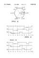
- FIG. 1is a schematic diagram of an electric motor and associated drive circuitry
- FIG. 2is a graph of waveforms of a coil during motoring
- FIG. 3is a graph of waveforms of a coil during regeneration
- FIG. 4is a vector state diagram of a motor drive vector computed from base vectors
- FIG. 5is a timing diagram showing a portion of one sequence of drive pulses.
- FIG. 6is a timing diagram showing a portion of another sequence of drive pulses.
- FIG. 1is a schematic diagram of an electric motor 101 and its associated drive circuitry configured for use in a motor vehicle, including coil drivers 111, 113 and 115, an interface circuit 117, a pulse generator 119, a memory circuit 121, a phase detector 123 and a sensor 137.
- Electric motor 101is shown as a three-phase motor having coils 131, 133 and 135 oriented at 0°, 120° and 240° angles within motor 101 and electrically coupled to a central node 157 as shown.
- Coils 131-135are respectively driven at nodes 151, 153 and 155 with drive pulse signals V 151 , V 153 and V 155 from the outputs of coil drivers 111-115.
- the pulses of V 151 -V 155have variable widths whose average duty cycles form envelopes that approximate the desired phase voltages at nodes 151-155. For convenience, these envelopes at nodes 151-155 are designated as VE 151 , VE 153 and VE 155 , respectively.
- the power factor of motor 101is set by the phases of I 131 -I 135 , which lag VE 151 -VE 155 in phase during motoring, i.e., when motor 101 delivers energy to the vehicle, and undergo an inversion in polarity so as to effectively lead in phase during regeneration, i.e., when motor 101 is receiving energy from the vehicle.
- pulse generator 119which comprises a microcontroller or similar circuit that operates by implementing software instructions stored in memory 121 as described below.
- Pulse generator 119computes one sequence during motoring operation and switches to another sequence while regenerating. The sequence being computed at any time is determined by a CONTROL signal produced by phase detector 123 to indicate the coil current phase.
- Sensor 137is disposed in motor 101 and includes an inductive pickup coil electromagnetically coupled for sensing I 131 flowing through coil 131. As shown in the figure, the reference direction of I 131 is out of the motor. Some applications use additional sensors to sense I 133 and I 135 as well. In an alternative embodiment, the phases of coil currents are determined from the rotor frequency with other types of sensors, such as optical sensing devices or Hall effect devices which produce sense pulses as the rotor passes. In addition, other physical states besides coil current, such as temperature, can be monitored and used to control motor 101. For example, temperature can be sensed with a thermocouple to produce a control signal to cause pulse generator 119 to switch to an idling drive pulse sequence if an elevated temperature is present. The present invention has a high degree of flexibility in improving the efficiency and reliability of motor 101 by monitoring such physical states and switching to an optimum drive pulse sequence when conditions warrant.
- Pulse generator 119computes V 151 -V 155 pulse widths from data stored in memory 121 which is indicative of the phase of VE 151 as described below. This phase data is applied to an input of phase detector 123 along with the sense signal from sensor 137 to produce CONTROL having one value when I 131 effectively leads VE 151 in phase and another value when I 131 lags VE 151 in phase.
- transistors 161-162are insulated gate bipolar transistors, so that the drive voltages applied to their respective gates are of opposite polarity to ensure that transistors 161-162 are not turned on at the same time.
- other types of semiconductor devicescan be used by appropriately modifying interface circuit 117. That is, when the voltage on output 171 of pulse generator 119 is logic high, the drive at node 181 is high while the drive on node 182 is low, or vice versa. A similar relationship exists between outputs 173 and 175 and nodes 183-184 and 185-186.
- Alternative configurationsare known and can be used to implement drivers 111-115.
- Phase detector 123is configured as a multiplier or other detection circuit which produces CONTROL at its output.
- CONTROLis applied to pulse generator 119 to switch "on-the-fly" from one sequence of drive pulses to another sequence optimized for the changed condition.
- Pulse generator 119produces a V 151 -V 155 drive pulse in each time period designated as T DRIVE .
- T DRIVEtime period designated as T DRIVE .
- V 151 -V 155 pulse widthsare computed for each T DRIVE to produce the desired phase.
- FIG. 2shows normalized representative waveforms of I 131 and VE 151 while motor 101 is motoring.
- VE 151is measured from node 151 to ground and is produced by a sequence of variable width drive pulses referred to as an alternating S 7 null sequence described in detail below.
- I 131is substantially sinusoidal, as is the voltage V COIL across coil 131, i.e., from node 151 to 157.
- the phase of I 131lags that of VE 151 .
- Similar waveformscan be obtained for VE 153 and VE 155 at nodes 153 and 155 and currents I 133 and I 135 through coils 133 and 135.
- the alternating S 7 null sequenceis used to provide not only a low overall amount of switching, but also to avoid switching coils while peak current is flowing through them.
- pulse generator 119produces a pulse at output 171 which remains at logic low throughout TP 3 -TP 4 to keep transistor 161 turned off and transistor 162 turned on. Hence, transistors 161-162 are not switched when I 131 is high, thereby substantially reduced transient power.
- FIG. 3is a similar graph of I 113 and VE 151 but while motor 101 is regenerating.
- VE 151is produced by a sequence referred to as an alternating S 0 null sequence described below. Note that the phase angle of I 131 leads that of VE 151 . Phase voltages VE 153 and VE 155 and currents I 133 and I 135 have similar waveforms. As is the case during motoring, VE 151 is not sinusoidal, whereas both I 131 and V COIL are sinusoidal.
- Transistor 161remains turned off while transistor 162 remains turned on.
- each of the nodes 151-155has two possible states, either V DRIVE (logic high or "1") or ground potential (logic low or "0").
- V DRIVElogic high or "1”
- ground potentiallogic low or "0”
- the 2 38 possible voltage combinations which can appear at nodes 151-155 are designated as base vectors S 0 -S 7 and listed in Table 1 below.
- base vector S 1(100) indicates that pulse generator 119 produces a logic high pulse at output 171 and logic low pulses at outputs 173 and 175.
- Interface circuit 117combines with drivers 111-115 to drive node 151 to V DRIVE and nodes 153-155 to ground.
- I 131splits at central node 157 and flows equally as I 133 and I 135 though coils 133 and 135. The higher current through coil 131 tends to orient the rotor of motor 101 to the 0° angle of coil 131.
- base vector S 4(011) drives node 151 to ground and nodes 153-155 to V DRIVE .
- I 131has the opposite polarity, again flowing equally through coils 133 and 135 to orient the rotor of motor 101 to an angle opposite to coil 131, or 180° as shown in Table 1.
- the other base vectorsproduce magnetic fields which tend to orient the rotor to angles indicated in the last column of Table 1.
- a combination of base vectorsis generated within a time period T DRIVE to drive motor 101 to other phase angles.
- null vector S 0 and S 7do not cause current to flow through coils 131-135.
- null vectors S 0 and S 7do not affect the angle of the rotor.
- the null vector chosencan determine the amount of switching in drivers 111-115, and therefore the power dissipated.
- FIG. 4is a vector state diagram showing graphically how SVM is used to compute drive pulses for an angle ⁇ from base vectors S 0 -S 7 .
- Base vectors S 1 -S 6define 60° regions or sectors of a cycle of motor 101, with their tips lying at the corners of a regular hexagon 201 as shown.
- Vector 210is directed at an angle ⁇ between adjacent base vectors S 1 and S 2 .
- the distance from the center of circle 203 to the perimeter of hexagon 201represents time period T DRIVE .
- Vector 210is resolved into component vectors 212 and 214 of base vectors S 1 and S 2 whose lengths represent pulse widths T S1 and T S2 within T DRIVE .
- a null vectoreither S 0 or S 7
- vector 210is generated by generating S 1 with a pulse width T S1 , S 2 with a pulse width T S2 and a null vector (S 0 or S 7 ) for the remaining period T DRIVE -(T S1 +T S2 ).
- Vectors lying in other sectorsare similarly computed from base vectors.
- a vector at an angle ⁇is generated by resolving into component vectors parallel to adjacent base vectors S i and S i+1 and having pulse widths T i and T i+1 , where i is an integer between one and six. Assuming base vector S i has a phase angle bit the pulse widths are computed from the following equations 1-4.
- a scale factor mis used to scale pulse widths T i and T i+1 within T DRIVE to adjust the power delivered to motor 101. Hence, m can be adjusted to produce a sequence for idling motor 101.
- the value of mis between zero and one.
- T 5corresponds to an angle of 60° to show the alternation of null vectors S 7 and S 0 .
- the interval T 0 -T 5lies in the 0°-60° sector, so pulse generator 119 uses base vectors S 1 and S 2 to compute pulse widths for V 151 -V 155 from equations 1-4.
- the V 151 -V 155 pulsesare center-aligned within T 0 -T 5 around midpoint T C to minimize the amount of simultaneous switching of drivers 111-115, which reduces system noise and harmonic jitter.
- one-half of S 2is generated during T 1 -T 2 and the other half during T 3 -T 4 .
- one-half of S 7is generated during T 0 -T 1 and the other half during T 4 -T 5 .
- S 1is generated during T 2 -T 3 .
- This vector sequenceis used for all T DRIVE time periods in the 0°-60° sector, which lies within interval TP 1 -TP 2 of FIG. 2 where I 131 is near peak levels. Note that V 151 is not switched during this period, but instead remains at a constant voltage V DRIVE . Pulse widths are varied in accordance with equations 1-4 to advance the phase angle through the sector.
- the time period T 5 -T 10occurs in the 60°-120° sector, and uses base vectors S 2 and S 3 to compute pulse widths of V 151 -V 155 from equations 1-4.
- V 151 -V 155are center-aligned as described above.
- Base vector S 2is produced during T 5 -T 6 , S 3 during T 6 -T 7 , null vector S 0 during T 7 -T 8 , S 3 during T 8 -T 9 and S 2 during T 9 -T 10 .
- null vector S 0is used in the 60°-120° sector, rather than S 7 as in the 0°60° sector.
- Table 2 belowshows vector angles, base vector sequences, and drive pulse sequences for the sectors.
- null vectoralternates between S 7 and S 0 in adjacent sectors.
- sectors 1, 3 and 5use null vector S 7
- sectors 2, 4 and 6use null vector S 0 .
- an alternating null sequence beginning with S 7has the advantage of minimizing switching transitions and power consumption when coil currents are at or near their peaks.
- T 5corresponds to a 60° phase angle to show the alternation of null vectors S 0 and S 7 .
- base vectors S 1 and S 2 and null vector S 0are used to compute V 151 -V 155 .
- base vectors S 2 and S 3 and null vector S 7are used.
- V 151 -V 155are computed by pulse generator 119 using equations 1-4 above, and then center-aligned within the period T 0 -T 5 around midpoint T C to minimize simultaneous switching.
- base vector S 2is generated from T 0 -T 1
- S 1is generated from T 1 -T 2
- null vector S 0is generated from T 2 -T 3
- S 1 from T 3 -T 4and S 2 from T 4 -T 5 .
- This sequenceis repeated in the other T DRIVE time periods within the 0°-60° sector, which lies within the interval TP 5 to TP 6 of FIG. 4 where I 131 is near its peak levels.
- V 151is not switched during this period, but instead remains at a constant ground potential throughout the 0°-60° sector.
- Time period T 5 T 10occurs in the 60°-120° sector and uses S 2 and S 3 to compute pulse widths of V 151 -V 155 from equations 1-4. To reduce simultaneous switching, V 151 -V 155 are center-aligned.
- null vector S 7is generated during T 5 -T 6 , base vector S 2 during T 6 -T 7 , S 3 from T 7 -T 8 , S 2 from T 8 to T 9 and null vector S 7 during T 9 -T 10 .
- null vector S 7is used in the 60°-120° sector, whereas S 0 is used in the 0°-60° sector.
- sectors 1, 3 and 5use null vector S 0
- sectors 2, 4 and 6use null vector S 7 .
- the alternating null S 0 sequencehas the advantage of minimizing driver switching and power consumption when coil currents are at or near their peaks.
- a pulse generatordrives the electric motor with a sequence of drive pulses over a series of time periods.
- the pulse widths of the drive pulsesare varied to represent phases of the electric motor.
- a physical state of the motorsuch as its power factor or temperature, is monitored by a sensor to produce a representative control signal.
- a physical statesuch as the motor's power factor can be used to generate one sequence of drive pulses while the motor is motoring and to switch to another sequence when the motor is regenerating.
- the pulse generatorresponds to the control signal by switching to another sequence of drive pulses to drive the motor.
Landscapes
- Engineering & Computer Science (AREA)
- Power Engineering (AREA)
- Transportation (AREA)
- Mechanical Engineering (AREA)
- Life Sciences & Earth Sciences (AREA)
- Sustainable Development (AREA)
- Sustainable Energy (AREA)
- Control Of Ac Motors In General (AREA)
Abstract
Description
TABLE 1 ______________________________________ Base Node NodeNode Phase Vector 151 153 Angle ______________________________________ Groundb Ground Ground Null S.sub.1 = 100 V.sub.DRIVE Ground Ground 0° S.sub.2 = 110 V.sub.DRIVE V.sub.DRIVE Ground 60° S.sub.3 = 010 Ground V.sub.DRIVE Ground 120° S.sub.4 = 011 Ground V.sub.DRIVE V.sub.DRIVE 180° S.sub.5 = 001 Ground Ground 240° S.sub.6 = 101 V.sub.DRIVE Ground 300° S.sub.7 = 111 V.sub.DRIVE V.sub.DRIVE V.sub.DRIVE Null ______________________________________
Θ=Φ-Φ.sub.I (1)
T.sub.i =m*T.sub.DRIVE *sin(60°-Θ) (2)
T/.sub.i+1 =m*T.sub.DRIVE *sin(Θ) (3)
T.sub.NULL =T.sub.DRIVE -(T.sub.i +T.sub.i+1) (4)
TABLE 2 ______________________________________ (V.sub.151 V.sub.153 V.sub.155) Sector Phase Angle Sequence Drive Pulse Sequence ______________________________________ 0°-60° S.sub.7 S.sub.2 S.sub.1 S.sub.2 S.sub.7 111,110,100,110,111 2 60°-120° S.sub.2 S.sub.3 S.sub.0 S.sub.3 S.sub.2 110,010,000,010,110 3 120°-180° S.sub.7 S.sub.4 S.sub.3 S.sub.4 S.sub.7 111,011,010,011,111 4 180°-240° S.sub.4 S.sub.5 S.sub.0 S.sub.5 S.sub.4 011,001,000,001,011 5 240°-300° S.sub.7 S.sub.6 S.sub.5 S.sub.6 S.sub.7 111,101,001,101,111 6 300°-360° S.sub.6 S.sub.5 S.sub.0 S.sub.5 S.sub.6 101,100,000,100,101 ______________________________________
TABLE 3 ______________________________________ (V.sub.151 V.sub.153 V.sub.155) Sector Phase Angle Sequence Drive Pulse Sequence ______________________________________ 1 0°-60° S.sub.2 S.sub.1 S.sub.0 S.sub.1 S.sub.2 110,100,000,100,110 2 60°-120° S.sub.7 S.sub.3 S.sub.2 S.sub.3 S.sub.7 111,010,110,010,110 3 120°-180° S.sub.4 S.sub.3 S.sub.0 S.sub.3 S.sub.4 011,010,000,010,011 4 180°-240° S.sub.7 S.sub.4 S.sub.5 S.sub.4 S.sub.7 111,011,001,011,111 5 240°-300° S.sub.6 S.sub.5 S.sub.0 S.sub.5 S.sub.6 101,001,000,001,101 6 300°-360° S.sub.7 S.sub.6 S.sub.1 S.sub.6 S.sub.7 111,101,100,101,111 ______________________________________
Claims (15)
Priority Applications (1)
| Application Number | Priority Date | Filing Date | Title |
|---|---|---|---|
| US08/980,422US6023136A (en) | 1997-11-28 | 1997-11-28 | Adaptive motor control circuit and method |
Applications Claiming Priority (1)
| Application Number | Priority Date | Filing Date | Title |
|---|---|---|---|
| US08/980,422US6023136A (en) | 1997-11-28 | 1997-11-28 | Adaptive motor control circuit and method |
Publications (1)
| Publication Number | Publication Date |
|---|---|
| US6023136Atrue US6023136A (en) | 2000-02-08 |
Family
ID=25527547
Family Applications (1)
| Application Number | Title | Priority Date | Filing Date |
|---|---|---|---|
| US08/980,422Expired - LifetimeUS6023136A (en) | 1997-11-28 | 1997-11-28 | Adaptive motor control circuit and method |
Country Status (1)
| Country | Link |
|---|---|
| US (1) | US6023136A (en) |
Cited By (12)
| Publication number | Priority date | Publication date | Assignee | Title |
|---|---|---|---|---|
| US6140782A (en)* | 1999-04-06 | 2000-10-31 | Silicon Touch Technology Inc. | Brushless DC fan driver with overshoot voltage prevention and enhanced operational efficiency |
| US20030173946A1 (en)* | 2002-03-15 | 2003-09-18 | Guang Liu | Procedure for measuring the current in each phase of a three-phase device via single current sensor |
| US20030210009A1 (en)* | 2002-05-10 | 2003-11-13 | Analog Devices, Inc. | Pulse width modulated drive system for electronically commutated motors |
| US20040039694A1 (en)* | 2001-05-29 | 2004-02-26 | American Express Travel Related Services Company, Inc. | System and method for facilitating a subsidiary card account with controlled spending capability |
| US20040232875A1 (en)* | 2003-05-20 | 2004-11-25 | Samsung Electronics Co., Ltd. | Apparatus and method for controlling inverter for driving a three-phase motor |
| US20040247299A1 (en)* | 2003-06-03 | 2004-12-09 | Murakami Corporation | Motor control device for vehicular power mirror |
| US20050007050A1 (en)* | 2003-07-07 | 2005-01-13 | Agere System Inc. | Hard drive spindle motor controller with reverse current prevention |
| US20050248361A1 (en)* | 2004-05-10 | 2005-11-10 | O'gorman Patrick A | Damping control in a three-phase motor with a single current sensor |
| US7839102B1 (en)* | 2005-01-07 | 2010-11-23 | Marvell International Ltd | System and process for utilizing back electromotive force in disk drives |
| CN105659492A (en)* | 2013-10-22 | 2016-06-08 | 大陆-特韦斯贸易合伙股份公司及两合公司 | Method for actuating a brushless motor |
| US20160264019A1 (en)* | 2014-03-10 | 2016-09-15 | Dean Drako | Distributed Motor Torque Generation System and Method of Control |
| US20190097568A1 (en)* | 2017-09-28 | 2019-03-28 | Itt Manufacturing Enterprises Llc. | Matrix converter motor winding temperature control with closed feedback loop |
Citations (13)
| Publication number | Priority date | Publication date | Assignee | Title |
|---|---|---|---|---|
| US4291265A (en)* | 1978-11-04 | 1981-09-22 | Fujitsu Fanuc Limited | Protective system for inverter circuit used in driving AC motors |
| US4314191A (en)* | 1978-11-04 | 1982-02-02 | Shigeki Kawada | Protective system for inverter circuit used in driving AC motors |
| US4727468A (en)* | 1984-08-22 | 1988-02-23 | Kabushiki Kaisha Toshiba | Digital PWM control circuit |
| US5264775A (en)* | 1991-09-09 | 1993-11-23 | General Motors Corporation | Pulse width modulation control apparatus and method |
| US5309079A (en)* | 1991-04-10 | 1994-05-03 | Matsushita Electric Industrial Co., Ltd. | Digital three-phase PWM signal |
| US5317243A (en)* | 1991-10-03 | 1994-05-31 | Sgs-Thomson Microelectronics, Inc. | Method and apparatus for detecting velocity profiles of a spinning rotor of a polyphase DC motor |
| US5334917A (en)* | 1990-07-12 | 1994-08-02 | W. Schlafhorst Ag & Co. | System and method for optimally driving a DC motor |
| US5350988A (en)* | 1990-07-10 | 1994-09-27 | Alliedsignal, Inc. | Digital motor controller |
| US5463299A (en)* | 1989-06-07 | 1995-10-31 | Hitachi, Ltd. | Current controller for controlling a current flowing in a load using a PWM inverter and method used thereby |
| US5486743A (en)* | 1992-11-19 | 1996-01-23 | Kabushiki Kaisha Toshiba | Inverter and air conditioner controlled by the same |
| US5491622A (en)* | 1994-01-07 | 1996-02-13 | Delco Electronics Corp. | Power converter with emergency operating mode for three phase induction motors |
| US5572097A (en)* | 1991-10-03 | 1996-11-05 | Sgs-Thomson Microelectronics, Inc. | Method and apparatus for starting polyphase dc motor |
| US5631999A (en)* | 1995-09-06 | 1997-05-20 | Seagate Technology Inc. | Adaptive compensation for hard disc drive spindle motor manufacturing tolerances |
- 1997
- 1997-11-28USUS08/980,422patent/US6023136A/ennot_activeExpired - Lifetime
Patent Citations (13)
| Publication number | Priority date | Publication date | Assignee | Title |
|---|---|---|---|---|
| US4314191A (en)* | 1978-11-04 | 1982-02-02 | Shigeki Kawada | Protective system for inverter circuit used in driving AC motors |
| US4291265A (en)* | 1978-11-04 | 1981-09-22 | Fujitsu Fanuc Limited | Protective system for inverter circuit used in driving AC motors |
| US4727468A (en)* | 1984-08-22 | 1988-02-23 | Kabushiki Kaisha Toshiba | Digital PWM control circuit |
| US5463299A (en)* | 1989-06-07 | 1995-10-31 | Hitachi, Ltd. | Current controller for controlling a current flowing in a load using a PWM inverter and method used thereby |
| US5350988A (en)* | 1990-07-10 | 1994-09-27 | Alliedsignal, Inc. | Digital motor controller |
| US5334917A (en)* | 1990-07-12 | 1994-08-02 | W. Schlafhorst Ag & Co. | System and method for optimally driving a DC motor |
| US5309079A (en)* | 1991-04-10 | 1994-05-03 | Matsushita Electric Industrial Co., Ltd. | Digital three-phase PWM signal |
| US5264775A (en)* | 1991-09-09 | 1993-11-23 | General Motors Corporation | Pulse width modulation control apparatus and method |
| US5317243A (en)* | 1991-10-03 | 1994-05-31 | Sgs-Thomson Microelectronics, Inc. | Method and apparatus for detecting velocity profiles of a spinning rotor of a polyphase DC motor |
| US5572097A (en)* | 1991-10-03 | 1996-11-05 | Sgs-Thomson Microelectronics, Inc. | Method and apparatus for starting polyphase dc motor |
| US5486743A (en)* | 1992-11-19 | 1996-01-23 | Kabushiki Kaisha Toshiba | Inverter and air conditioner controlled by the same |
| US5491622A (en)* | 1994-01-07 | 1996-02-13 | Delco Electronics Corp. | Power converter with emergency operating mode for three phase induction motors |
| US5631999A (en)* | 1995-09-06 | 1997-05-20 | Seagate Technology Inc. | Adaptive compensation for hard disc drive spindle motor manufacturing tolerances |
Non-Patent Citations (16)
| Title |
|---|
| "A Novel Digital Control For Active Power Filter", E. H. Song et al., IEEE, 0-7803-0582-5/92, pp. 1168-1173. |
| "Power Losses For Space Vector Modulation Techniques", Perruchoud et al., 1996 IEEE, 0-7803-3292-X/96, pp. 167-173. |
| "Space Vector Fourier Analysis Of SVM Inverters In The Overmodulation Range", s. Bolognani et al., IEEE, 0-7803-2795-0, pp. 319-324. |
| "Space Vector Modulated matrix Converter With Minimized Number Of Switchings And a Feedforward Compensation Of Input Voltage Unbalance", P. Nielsen et al, IEEE, 0-7803-2795, pp. 833-839. |
| "The Microprocessor Based Modifised Space Vector Control Of The Matrix Converter", E.M. Chekhet et al., Institute of Electrodynamics of the Unkrainian National Academy of Sciences, Kiev, Ukraine. |
| A Novel Digital Control For Active Power Filter , E. H. Song et al., IEEE, 0 7803 0582 5/92, pp. 1168 1173.* |
| G. Ledwich, IEEE Transactions on Power Electronics, "Current Source Inverter Modulation", vol. 6, No. 4, Oct. 1991, pp. 618-623. |
| G. Ledwich, IEEE Transactions on Power Electronics, Current Source Inverter Modulation , vol. 6, No. 4, Oct. 1991, pp. 618 623.* |
| P. Pinewski, EDN Products Edition, "Understanding Space Vector Modulation", Mar. 7, 1996, pp. 45-46. |
| P. Pinewski, EDN Products Edition, Understanding Space Vector Modulation , Mar. 7, 1996, pp. 45 46.* |
| Power Losses For Space Vector Modulation Techniques , Perruchoud et al., 1996 IEEE, 0 7803 3292 X/96, pp. 167 173.* |
| S. Fukuda et al., IEEE Transactions on Power Electronics, "PWM Technique for Inverter with Sinusoidal Output Current", vol. 5, No. 1, Jan. 1990, pp. 54-61. |
| S. Fukuda et al., IEEE Transactions on Power Electronics, PWM Technique for Inverter with Sinusoidal Output Current , vol. 5, No. 1, Jan. 1990, pp. 54 61.* |
| Space Vector Fourier Analysis Of SVM Inverters In The Overmodulation Range , s. Bolognani et al., IEEE, 0 7803 2795 0, pp. 319 324.* |
| Space Vector Modulated matrix Converter With Minimized Number Of Switchings And a Feedforward Compensation Of Input Voltage Unbalance , P. Nielsen et al, IEEE, 0 7803 2795, pp. 833 839.* |
| The Microprocessor Based Modifised Space Vector Control Of The Matrix Converter , E.M. Chekhet et al., Institute of Electrodynamics of the Unkrainian National Academy of Sciences, Kiev, Ukraine.* |
Cited By (22)
| Publication number | Priority date | Publication date | Assignee | Title |
|---|---|---|---|---|
| US6140782A (en)* | 1999-04-06 | 2000-10-31 | Silicon Touch Technology Inc. | Brushless DC fan driver with overshoot voltage prevention and enhanced operational efficiency |
| US20040039694A1 (en)* | 2001-05-29 | 2004-02-26 | American Express Travel Related Services Company, Inc. | System and method for facilitating a subsidiary card account with controlled spending capability |
| US20030173946A1 (en)* | 2002-03-15 | 2003-09-18 | Guang Liu | Procedure for measuring the current in each phase of a three-phase device via single current sensor |
| US6735537B2 (en)* | 2002-03-15 | 2004-05-11 | Motorola, Inc. | Procedure for measuring the current in each phase of a three-phase device via single current sensor |
| US20030210009A1 (en)* | 2002-05-10 | 2003-11-13 | Analog Devices, Inc. | Pulse width modulated drive system for electronically commutated motors |
| US20040232875A1 (en)* | 2003-05-20 | 2004-11-25 | Samsung Electronics Co., Ltd. | Apparatus and method for controlling inverter for driving a three-phase motor |
| US6911801B2 (en) | 2003-05-20 | 2005-06-28 | Samsung Electronics Co., Ltd | Apparatus and method for controlling inverter for driving a three-phase motor |
| US6983102B2 (en)* | 2003-06-03 | 2006-01-03 | Murakami Corporation | Motor control device for vehicular power mirror |
| US20040247299A1 (en)* | 2003-06-03 | 2004-12-09 | Murakami Corporation | Motor control device for vehicular power mirror |
| US20050007050A1 (en)* | 2003-07-07 | 2005-01-13 | Agere System Inc. | Hard drive spindle motor controller with reverse current prevention |
| US6917172B2 (en)* | 2003-07-07 | 2005-07-12 | Agere Systems Inc. | Hard drive spindle motor controller with reverse current prevention |
| US20050248361A1 (en)* | 2004-05-10 | 2005-11-10 | O'gorman Patrick A | Damping control in a three-phase motor with a single current sensor |
| US7414425B2 (en) | 2004-05-10 | 2008-08-19 | Temic Automotive Of North America, Inc. | Damping control in a three-phase motor with a single current sensor |
| US7839102B1 (en)* | 2005-01-07 | 2010-11-23 | Marvell International Ltd | System and process for utilizing back electromotive force in disk drives |
| CN105659492A (en)* | 2013-10-22 | 2016-06-08 | 大陆-特韦斯贸易合伙股份公司及两合公司 | Method for actuating a brushless motor |
| US20160261221A1 (en)* | 2013-10-22 | 2016-09-08 | Continental Teves Ag & Co. Ohg | Method for actuating a brushless motor |
| US9716462B2 (en)* | 2013-10-22 | 2017-07-25 | Continental Teves Ag & Co. Ohg | Method for actuating a brushless motor |
| CN105659492B (en)* | 2013-10-22 | 2018-10-02 | 大陆-特韦斯贸易合伙股份公司及两合公司 | Method for controlling brushless motor |
| US20160264019A1 (en)* | 2014-03-10 | 2016-09-15 | Dean Drako | Distributed Motor Torque Generation System and Method of Control |
| US9744879B2 (en)* | 2014-03-10 | 2017-08-29 | R Motor Company | Distributed motor torque generation system and method of control |
| US20190097568A1 (en)* | 2017-09-28 | 2019-03-28 | Itt Manufacturing Enterprises Llc. | Matrix converter motor winding temperature control with closed feedback loop |
| US10833626B2 (en)* | 2017-09-28 | 2020-11-10 | Itt Manufacturing Enterprises Llc | Matrix converter motor winding temperature control with closed feedback loop |
Similar Documents
| Publication | Publication Date | Title |
|---|---|---|
| FI115011B (en) | Operating system for brushless DC motor | |
| JP7074144B2 (en) | Rotating electric machine control device | |
| US7075267B1 (en) | Space vector-based current controlled PWM inverter for motor drives | |
| US5677605A (en) | Brushless DC motor using phase timing advancement | |
| US7088595B2 (en) | Reversible buck-boost chopper circuit, and inverter circuit with the same | |
| JP3710602B2 (en) | Power generator | |
| US7294984B2 (en) | Motor controller | |
| US6023136A (en) | Adaptive motor control circuit and method | |
| US6661206B2 (en) | Soft chopping for switched reluctance generators | |
| MXPA97000154A (en) | Direct current motor or continuous synchronizer, using a synchronized progress dela f | |
| JPH0429312B2 (en) | ||
| WO2020045636A1 (en) | Rotating electrical machine control device | |
| TW202110073A (en) | Motor driving circuit and method thereof | |
| CN111416552B (en) | A flexible permanent magnet brushless DC motor control system and control method thereof | |
| US20200304049A1 (en) | Pulse width modulation pattern generator and corresponding systems, methods and computer programs | |
| US6465973B1 (en) | Permanent magnet 2-phase DC brushless motor | |
| US6661190B1 (en) | Controller and associated drive assembly controlling a brushless direct current motor | |
| US6323610B1 (en) | Silent spin sine wave generator | |
| US6040989A (en) | Device and method for generating three-phase sine waves using two pulse-width modulators | |
| US20240291417A1 (en) | Inverter control device and inverter control method | |
| JP7534983B2 (en) | Inverter control device | |
| JP4779233B2 (en) | Brushless motor drive control device | |
| JP3258743B2 (en) | Brushless motor drive | |
| JP3552380B2 (en) | Brushless motor drive | |
| JP4140500B2 (en) | Two-phase modulation control type inverter device |
Legal Events
| Date | Code | Title | Description |
|---|---|---|---|
| AS | Assignment | Owner name:MOTOROLA, INC., ILLINOIS Free format text:ASSIGNMENT OF ASSIGNORS INTEREST;ASSIGNOR:PINEWSKI, PETER J.;REEL/FRAME:008851/0363 Effective date:19971124 | |
| AS | Assignment | Owner name:MAZDA MOTOR CORPORATION, JAPAN Free format text:ASSIGNMENT OF ASSIGNORS INTEREST;ASSIGNORS:SHIGIHAMA, SHINGO;HOSOKAI, TETSUSHI;KAMAKURA, TAMOTSU;AND OTHERS;REEL/FRAME:009253/0986;SIGNING DATES FROM 19980515 TO 19980519 | |
| STCF | Information on status: patent grant | Free format text:PATENTED CASE | |
| FPAY | Fee payment | Year of fee payment:4 | |
| AS | Assignment | Owner name:FREESCALE SEMICONDUCTOR, INC., TEXAS Free format text:ASSIGNMENT OF ASSIGNORS INTEREST;ASSIGNOR:MOTOROLA, INC.;REEL/FRAME:015698/0657 Effective date:20040404 Owner name:FREESCALE SEMICONDUCTOR, INC.,TEXAS Free format text:ASSIGNMENT OF ASSIGNORS INTEREST;ASSIGNOR:MOTOROLA, INC.;REEL/FRAME:015698/0657 Effective date:20040404 | |
| AS | Assignment | Owner name:CITIBANK, N.A. AS COLLATERAL AGENT, NEW YORK Free format text:SECURITY AGREEMENT;ASSIGNORS:FREESCALE SEMICONDUCTOR, INC.;FREESCALE ACQUISITION CORPORATION;FREESCALE ACQUISITION HOLDINGS CORP.;AND OTHERS;REEL/FRAME:018855/0129 Effective date:20061201 Owner name:CITIBANK, N.A. AS COLLATERAL AGENT,NEW YORK Free format text:SECURITY AGREEMENT;ASSIGNORS:FREESCALE SEMICONDUCTOR, INC.;FREESCALE ACQUISITION CORPORATION;FREESCALE ACQUISITION HOLDINGS CORP.;AND OTHERS;REEL/FRAME:018855/0129 Effective date:20061201 | |
| FPAY | Fee payment | Year of fee payment:8 | |
| AS | Assignment | Owner name:CITIBANK, N.A., AS COLLATERAL AGENT,NEW YORK Free format text:SECURITY AGREEMENT;ASSIGNOR:FREESCALE SEMICONDUCTOR, INC.;REEL/FRAME:024397/0001 Effective date:20100413 Owner name:CITIBANK, N.A., AS COLLATERAL AGENT, NEW YORK Free format text:SECURITY AGREEMENT;ASSIGNOR:FREESCALE SEMICONDUCTOR, INC.;REEL/FRAME:024397/0001 Effective date:20100413 | |
| FPAY | Fee payment | Year of fee payment:12 | |
| AS | Assignment | Owner name:CITIBANK, N.A., AS NOTES COLLATERAL AGENT, NEW YORK Free format text:SECURITY AGREEMENT;ASSIGNOR:FREESCALE SEMICONDUCTOR, INC.;REEL/FRAME:030633/0424 Effective date:20130521 Owner name:CITIBANK, N.A., AS NOTES COLLATERAL AGENT, NEW YOR Free format text:SECURITY AGREEMENT;ASSIGNOR:FREESCALE SEMICONDUCTOR, INC.;REEL/FRAME:030633/0424 Effective date:20130521 | |
| AS | Assignment | Owner name:CITIBANK, N.A., AS NOTES COLLATERAL AGENT, NEW YORK Free format text:SECURITY AGREEMENT;ASSIGNOR:FREESCALE SEMICONDUCTOR, INC.;REEL/FRAME:031591/0266 Effective date:20131101 Owner name:CITIBANK, N.A., AS NOTES COLLATERAL AGENT, NEW YOR Free format text:SECURITY AGREEMENT;ASSIGNOR:FREESCALE SEMICONDUCTOR, INC.;REEL/FRAME:031591/0266 Effective date:20131101 | |
| AS | Assignment | Owner name:FREESCALE SEMICONDUCTOR, INC., TEXAS Free format text:PATENT RELEASE;ASSIGNOR:CITIBANK, N.A., AS COLLATERAL AGENT;REEL/FRAME:037356/0143 Effective date:20151207 Owner name:FREESCALE SEMICONDUCTOR, INC., TEXAS Free format text:PATENT RELEASE;ASSIGNOR:CITIBANK, N.A., AS COLLATERAL AGENT;REEL/FRAME:037354/0225 Effective date:20151207 Owner name:FREESCALE SEMICONDUCTOR, INC., TEXAS Free format text:PATENT RELEASE;ASSIGNOR:CITIBANK, N.A., AS COLLATERAL AGENT;REEL/FRAME:037356/0553 Effective date:20151207 | |
| AS | Assignment | Owner name:MORGAN STANLEY SENIOR FUNDING, INC., MARYLAND Free format text:ASSIGNMENT AND ASSUMPTION OF SECURITY INTEREST IN PATENTS;ASSIGNOR:CITIBANK, N.A.;REEL/FRAME:037486/0517 Effective date:20151207 | |
| AS | Assignment | Owner name:MORGAN STANLEY SENIOR FUNDING, INC., MARYLAND Free format text:ASSIGNMENT AND ASSUMPTION OF SECURITY INTEREST IN PATENTS;ASSIGNOR:CITIBANK, N.A.;REEL/FRAME:037518/0292 Effective date:20151207 | |
| AS | Assignment | Owner name:MORGAN STANLEY SENIOR FUNDING, INC., MARYLAND Free format text:SUPPLEMENT TO THE SECURITY AGREEMENT;ASSIGNOR:FREESCALE SEMICONDUCTOR, INC.;REEL/FRAME:039138/0001 Effective date:20160525 | |
| AS | Assignment | Owner name:NXP, B.V., F/K/A FREESCALE SEMICONDUCTOR, INC., NETHERLANDS Free format text:RELEASE BY SECURED PARTY;ASSIGNOR:MORGAN STANLEY SENIOR FUNDING, INC.;REEL/FRAME:040925/0001 Effective date:20160912 Owner name:NXP, B.V., F/K/A FREESCALE SEMICONDUCTOR, INC., NE Free format text:RELEASE BY SECURED PARTY;ASSIGNOR:MORGAN STANLEY SENIOR FUNDING, INC.;REEL/FRAME:040925/0001 Effective date:20160912 | |
| AS | Assignment | Owner name:NXP B.V., NETHERLANDS Free format text:RELEASE BY SECURED PARTY;ASSIGNOR:MORGAN STANLEY SENIOR FUNDING, INC.;REEL/FRAME:040928/0001 Effective date:20160622 | |
| AS | Assignment | Owner name:NXP USA, INC., TEXAS Free format text:CHANGE OF NAME;ASSIGNOR:FREESCALE SEMICONDUCTOR, INC.;REEL/FRAME:040652/0241 Effective date:20161107 Owner name:NXP USA, INC., TEXAS Free format text:MERGER;ASSIGNOR:FREESCALE SEMICONDUCTOR, INC.;REEL/FRAME:040652/0241 Effective date:20161107 | |
| AS | Assignment | Owner name:NXP USA, INC., TEXAS Free format text:CORRECTIVE ASSIGNMENT TO CORRECT THE NATURE OF CONVEYANCE PREVIOUSLY RECORDED AT REEL: 040652 FRAME: 0241. ASSIGNOR(S) HEREBY CONFIRMS THE MERGER AND CHANGE OF NAME;ASSIGNOR:FREESCALE SEMICONDUCTOR, INC.;REEL/FRAME:041260/0850 Effective date:20161107 | |
| AS | Assignment | Owner name:MORGAN STANLEY SENIOR FUNDING, INC., MARYLAND Free format text:CORRECTIVE ASSIGNMENT TO CORRECT THE REMOVE PATENTS 8108266 AND 8062324 AND REPLACE THEM WITH 6108266 AND 8060324 PREVIOUSLY RECORDED ON REEL 037518 FRAME 0292. ASSIGNOR(S) HEREBY CONFIRMS THE ASSIGNMENT AND ASSUMPTION OF SECURITY INTEREST IN PATENTS;ASSIGNOR:CITIBANK, N.A.;REEL/FRAME:041703/0536 Effective date:20151207 | |
| AS | Assignment | Owner name:SHENZHEN XINGUODU TECHNOLOGY CO., LTD., CHINA Free format text:CORRECTIVE ASSIGNMENT TO CORRECT THE TO CORRECT THE APPLICATION NO. FROM 13,883,290 TO 13,833,290 PREVIOUSLY RECORDED ON REEL 041703 FRAME 0536. ASSIGNOR(S) HEREBY CONFIRMS THE THE ASSIGNMENT AND ASSUMPTION OF SECURITYINTEREST IN PATENTS.;ASSIGNOR:MORGAN STANLEY SENIOR FUNDING, INC.;REEL/FRAME:048734/0001 Effective date:20190217 | |
| AS | Assignment | Owner name:NXP B.V., NETHERLANDS Free format text:RELEASE BY SECURED PARTY;ASSIGNOR:MORGAN STANLEY SENIOR FUNDING, INC.;REEL/FRAME:050744/0097 Effective date:20190903 | |
| AS | Assignment | Owner name:MORGAN STANLEY SENIOR FUNDING, INC., MARYLAND Free format text:CORRECTIVE ASSIGNMENT TO CORRECT THE REMOVE APPLICATION11759915 AND REPLACE IT WITH APPLICATION 11759935 PREVIOUSLY RECORDED ON REEL 037486 FRAME 0517. ASSIGNOR(S) HEREBY CONFIRMS THE ASSIGNMENT AND ASSUMPTION OF SECURITYINTEREST IN PATENTS;ASSIGNOR:CITIBANK, N.A.;REEL/FRAME:053547/0421 Effective date:20151207 | |
| AS | Assignment | Owner name:NXP B.V., NETHERLANDS Free format text:CORRECTIVE ASSIGNMENT TO CORRECT THE REMOVEAPPLICATION 11759915 AND REPLACE IT WITH APPLICATION11759935 PREVIOUSLY RECORDED ON REEL 040928 FRAME 0001. ASSIGNOR(S) HEREBY CONFIRMS THE RELEASE OF SECURITYINTEREST;ASSIGNOR:MORGAN STANLEY SENIOR FUNDING, INC.;REEL/FRAME:052915/0001 Effective date:20160622 | |
| AS | Assignment | Owner name:NXP, B.V. F/K/A FREESCALE SEMICONDUCTOR, INC., NETHERLANDS Free format text:CORRECTIVE ASSIGNMENT TO CORRECT THE REMOVEAPPLICATION 11759915 AND REPLACE IT WITH APPLICATION11759935 PREVIOUSLY RECORDED ON REEL 040925 FRAME 0001. ASSIGNOR(S) HEREBY CONFIRMS THE RELEASE OF SECURITYINTEREST;ASSIGNOR:MORGAN STANLEY SENIOR FUNDING, INC.;REEL/FRAME:052917/0001 Effective date:20160912 |