US6022482A - Monolithic ink jet printhead - Google Patents
Monolithic ink jet printheadDownload PDFInfo
- Publication number
- US6022482A US6022482AUS08/905,759US90575997AUS6022482AUS 6022482 AUS6022482 AUS 6022482AUS 90575997 AUS90575997 AUS 90575997AUS 6022482 AUS6022482 AUS 6022482A
- Authority
- US
- United States
- Prior art keywords
- printhead
- nozzles
- ink
- layer
- top surface
- Prior art date
- Legal status (The legal status is an assumption and is not a legal conclusion. Google has not performed a legal analysis and makes no representation as to the accuracy of the status listed.)
- Expired - Lifetime
Links
Images


Classifications
- B—PERFORMING OPERATIONS; TRANSPORTING
- B41—PRINTING; LINING MACHINES; TYPEWRITERS; STAMPS
- B41J—TYPEWRITERS; SELECTIVE PRINTING MECHANISMS, i.e. MECHANISMS PRINTING OTHERWISE THAN FROM A FORME; CORRECTION OF TYPOGRAPHICAL ERRORS
- B41J2/00—Typewriters or selective printing mechanisms characterised by the printing or marking process for which they are designed
- B41J2/005—Typewriters or selective printing mechanisms characterised by the printing or marking process for which they are designed characterised by bringing liquid or particles selectively into contact with a printing material
- B41J2/01—Ink jet
- B41J2/135—Nozzles
- B41J2/14—Structure thereof only for on-demand ink jet heads
- B41J2/1433—Structure of nozzle plates
- B—PERFORMING OPERATIONS; TRANSPORTING
- B41—PRINTING; LINING MACHINES; TYPEWRITERS; STAMPS
- B41J—TYPEWRITERS; SELECTIVE PRINTING MECHANISMS, i.e. MECHANISMS PRINTING OTHERWISE THAN FROM A FORME; CORRECTION OF TYPOGRAPHICAL ERRORS
- B41J2/00—Typewriters or selective printing mechanisms characterised by the printing or marking process for which they are designed
- B41J2/005—Typewriters or selective printing mechanisms characterised by the printing or marking process for which they are designed characterised by bringing liquid or particles selectively into contact with a printing material
- B41J2/01—Ink jet
- B41J2/135—Nozzles
- B41J2/14—Structure thereof only for on-demand ink jet heads
- B41J2/14016—Structure of bubble jet print heads
- B41J2/14072—Electrical connections, e.g. details on electrodes, connecting the chip to the outside...
- B—PERFORMING OPERATIONS; TRANSPORTING
- B41—PRINTING; LINING MACHINES; TYPEWRITERS; STAMPS
- B41J—TYPEWRITERS; SELECTIVE PRINTING MECHANISMS, i.e. MECHANISMS PRINTING OTHERWISE THAN FROM A FORME; CORRECTION OF TYPOGRAPHICAL ERRORS
- B41J2/00—Typewriters or selective printing mechanisms characterised by the printing or marking process for which they are designed
- B41J2/005—Typewriters or selective printing mechanisms characterised by the printing or marking process for which they are designed characterised by bringing liquid or particles selectively into contact with a printing material
- B41J2/01—Ink jet
- B41J2/135—Nozzles
- B41J2/14—Structure thereof only for on-demand ink jet heads
- B41J2/14016—Structure of bubble jet print heads
- B41J2/14088—Structure of heating means
- B41J2/14112—Resistive element
- B41J2/14129—Layer structure
- B—PERFORMING OPERATIONS; TRANSPORTING
- B41—PRINTING; LINING MACHINES; TYPEWRITERS; STAMPS
- B41J—TYPEWRITERS; SELECTIVE PRINTING MECHANISMS, i.e. MECHANISMS PRINTING OTHERWISE THAN FROM A FORME; CORRECTION OF TYPOGRAPHICAL ERRORS
- B41J2/00—Typewriters or selective printing mechanisms characterised by the printing or marking process for which they are designed
- B41J2/005—Typewriters or selective printing mechanisms characterised by the printing or marking process for which they are designed characterised by bringing liquid or particles selectively into contact with a printing material
- B41J2/01—Ink jet
- B41J2/135—Nozzles
- B41J2/16—Production of nozzles
- B41J2/1601—Production of bubble jet print heads
- B41J2/1603—Production of bubble jet print heads of the front shooter type
- B—PERFORMING OPERATIONS; TRANSPORTING
- B41—PRINTING; LINING MACHINES; TYPEWRITERS; STAMPS
- B41J—TYPEWRITERS; SELECTIVE PRINTING MECHANISMS, i.e. MECHANISMS PRINTING OTHERWISE THAN FROM A FORME; CORRECTION OF TYPOGRAPHICAL ERRORS
- B41J2/00—Typewriters or selective printing mechanisms characterised by the printing or marking process for which they are designed
- B41J2/005—Typewriters or selective printing mechanisms characterised by the printing or marking process for which they are designed characterised by bringing liquid or particles selectively into contact with a printing material
- B41J2/01—Ink jet
- B41J2/135—Nozzles
- B41J2/16—Production of nozzles
- B41J2/1621—Manufacturing processes
- B41J2/1626—Manufacturing processes etching
- B41J2/1628—Manufacturing processes etching dry etching
- B—PERFORMING OPERATIONS; TRANSPORTING
- B41—PRINTING; LINING MACHINES; TYPEWRITERS; STAMPS
- B41J—TYPEWRITERS; SELECTIVE PRINTING MECHANISMS, i.e. MECHANISMS PRINTING OTHERWISE THAN FROM A FORME; CORRECTION OF TYPOGRAPHICAL ERRORS
- B41J2/00—Typewriters or selective printing mechanisms characterised by the printing or marking process for which they are designed
- B41J2/005—Typewriters or selective printing mechanisms characterised by the printing or marking process for which they are designed characterised by bringing liquid or particles selectively into contact with a printing material
- B41J2/01—Ink jet
- B41J2/135—Nozzles
- B41J2/16—Production of nozzles
- B41J2/1621—Manufacturing processes
- B41J2/1626—Manufacturing processes etching
- B41J2/1629—Manufacturing processes etching wet etching
- B—PERFORMING OPERATIONS; TRANSPORTING
- B41—PRINTING; LINING MACHINES; TYPEWRITERS; STAMPS
- B41J—TYPEWRITERS; SELECTIVE PRINTING MECHANISMS, i.e. MECHANISMS PRINTING OTHERWISE THAN FROM A FORME; CORRECTION OF TYPOGRAPHICAL ERRORS
- B41J2/00—Typewriters or selective printing mechanisms characterised by the printing or marking process for which they are designed
- B41J2/005—Typewriters or selective printing mechanisms characterised by the printing or marking process for which they are designed characterised by bringing liquid or particles selectively into contact with a printing material
- B41J2/01—Ink jet
- B41J2/135—Nozzles
- B41J2/16—Production of nozzles
- B41J2/1621—Manufacturing processes
- B41J2/1631—Manufacturing processes photolithography
- B—PERFORMING OPERATIONS; TRANSPORTING
- B41—PRINTING; LINING MACHINES; TYPEWRITERS; STAMPS
- B41J—TYPEWRITERS; SELECTIVE PRINTING MECHANISMS, i.e. MECHANISMS PRINTING OTHERWISE THAN FROM A FORME; CORRECTION OF TYPOGRAPHICAL ERRORS
- B41J2/00—Typewriters or selective printing mechanisms characterised by the printing or marking process for which they are designed
- B41J2/005—Typewriters or selective printing mechanisms characterised by the printing or marking process for which they are designed characterised by bringing liquid or particles selectively into contact with a printing material
- B41J2/01—Ink jet
- B41J2/135—Nozzles
- B41J2/16—Production of nozzles
- B41J2/1621—Manufacturing processes
- B41J2/1637—Manufacturing processes molding
- B41J2/1639—Manufacturing processes molding sacrificial molding
- B—PERFORMING OPERATIONS; TRANSPORTING
- B41—PRINTING; LINING MACHINES; TYPEWRITERS; STAMPS
- B41J—TYPEWRITERS; SELECTIVE PRINTING MECHANISMS, i.e. MECHANISMS PRINTING OTHERWISE THAN FROM A FORME; CORRECTION OF TYPOGRAPHICAL ERRORS
- B41J2/00—Typewriters or selective printing mechanisms characterised by the printing or marking process for which they are designed
- B41J2/005—Typewriters or selective printing mechanisms characterised by the printing or marking process for which they are designed characterised by bringing liquid or particles selectively into contact with a printing material
- B41J2/01—Ink jet
- B41J2/135—Nozzles
- B41J2/16—Production of nozzles
- B41J2/1621—Manufacturing processes
- B41J2/164—Manufacturing processes thin film formation
- B41J2/1642—Manufacturing processes thin film formation thin film formation by CVD [chemical vapor deposition]
- B—PERFORMING OPERATIONS; TRANSPORTING
- B41—PRINTING; LINING MACHINES; TYPEWRITERS; STAMPS
- B41J—TYPEWRITERS; SELECTIVE PRINTING MECHANISMS, i.e. MECHANISMS PRINTING OTHERWISE THAN FROM A FORME; CORRECTION OF TYPOGRAPHICAL ERRORS
- B41J2/00—Typewriters or selective printing mechanisms characterised by the printing or marking process for which they are designed
- B41J2/005—Typewriters or selective printing mechanisms characterised by the printing or marking process for which they are designed characterised by bringing liquid or particles selectively into contact with a printing material
- B41J2/01—Ink jet
- B41J2/135—Nozzles
- B41J2/16—Production of nozzles
- B41J2/1621—Manufacturing processes
- B41J2/164—Manufacturing processes thin film formation
- B41J2/1645—Manufacturing processes thin film formation thin film formation by spincoating
- B—PERFORMING OPERATIONS; TRANSPORTING
- B41—PRINTING; LINING MACHINES; TYPEWRITERS; STAMPS
- B41J—TYPEWRITERS; SELECTIVE PRINTING MECHANISMS, i.e. MECHANISMS PRINTING OTHERWISE THAN FROM A FORME; CORRECTION OF TYPOGRAPHICAL ERRORS
- B41J2/00—Typewriters or selective printing mechanisms characterised by the printing or marking process for which they are designed
- B41J2/005—Typewriters or selective printing mechanisms characterised by the printing or marking process for which they are designed characterised by bringing liquid or particles selectively into contact with a printing material
- B41J2/01—Ink jet
- B41J2/135—Nozzles
- B41J2/16—Production of nozzles
- B41J2/1621—Manufacturing processes
- B41J2/164—Manufacturing processes thin film formation
- B41J2/1646—Manufacturing processes thin film formation thin film formation by sputtering
- B—PERFORMING OPERATIONS; TRANSPORTING
- B41—PRINTING; LINING MACHINES; TYPEWRITERS; STAMPS
- B41J—TYPEWRITERS; SELECTIVE PRINTING MECHANISMS, i.e. MECHANISMS PRINTING OTHERWISE THAN FROM A FORME; CORRECTION OF TYPOGRAPHICAL ERRORS
- B41J2/00—Typewriters or selective printing mechanisms characterised by the printing or marking process for which they are designed
- B41J2/005—Typewriters or selective printing mechanisms characterised by the printing or marking process for which they are designed characterised by bringing liquid or particles selectively into contact with a printing material
- B41J2/01—Ink jet
- B41J2/135—Nozzles
- B41J2/14—Structure thereof only for on-demand ink jet heads
- B41J2002/14475—Structure thereof only for on-demand ink jet heads characterised by nozzle shapes or number of orifices per chamber
- B—PERFORMING OPERATIONS; TRANSPORTING
- B41—PRINTING; LINING MACHINES; TYPEWRITERS; STAMPS
- B41J—TYPEWRITERS; SELECTIVE PRINTING MECHANISMS, i.e. MECHANISMS PRINTING OTHERWISE THAN FROM A FORME; CORRECTION OF TYPOGRAPHICAL ERRORS
- B41J2202/00—Embodiments of or processes related to ink-jet or thermal heads
- B41J2202/01—Embodiments of or processes related to ink-jet heads
- B41J2202/13—Heads having an integrated circuit
Definitions
- This inventionrelates to ink jet printheads and, more particularly, to a monolithic ink jet printhead comprising a polyimide manifold overlying a silicon substrate.
- Ink jet printershave come to dominate the lower end printing market due to its low cost (relative to laser printers), reduced noise and simpler printing apparatus. Furthermore, the print quality including color prints of ink jet printers has been approaching that of the laser printers.
- Ink jet printers, or plotters, of the so-called "drop-on-demand" typehave at least one printhead from which droplets of ink are directed towards a recording medium.
- the inkis contained in a plurality of channels and energy pulses are applied to transducers to cause the droplets of ink to be expelled, as required, from nozzles at the ends of the channels.
- thermal drop-on-demand ink jet printheadsThere are two general configurations for thermal drop-on-demand ink jet printheads.
- dropletsare propelled from nozzles formed in the printhead front face in a direction parallel to the flow of ink in ink channels and parallel to the surface of the bubble-generating heating elements of the printhead, such as, for example, the printhead configuration disclosed in U.S. Pat. Re. No. 32,572.
- This configurationis sometimes referred to as an edge shooter or a side shooter.
- the other thermal ink jet configurationpropels droplets from nozzles in a direction normal to the surface of the bubble-generating heating elements, such as, for example, the printhead disclosed in U.S. Pat. No. 4,568,953.
- This configurationis sometimes referred to as a roofshooter.
- a defining difference between the two configurationslies in the direction of droplet ejection, in that the side shooter configuration ejects droplets in the plane of the substrate having the heating elements, whereas the roofshooter ejects droplets out of the plane of the substrate having the heating elements and in a direction normal thereto.
- a roofshooter printhead of the type disclosed in U.S. Pat. No. 4,568,953is a hybrid design which uses an electroplating technique to form a nickel nozzle array on the surface of a silicon substrate containing ink channels, resistors and electrical connections.
- This nozzle plate designlimits achieving the high density of nozzles required to reach laser like print quality.
- Substrate fabrication techniquesare also subject to low yields.
- these, and other beneficial featuresare realized by using a highly miniaturized and integrated silicon micromachining technique for fabricating a monolithic roofshooter type printhead. No substrate bonding is required offering yield advantages.
- direct integration of addressing circuitry on printheadis accomplished. The feasibility of integrating addressing circuitry on-chip enables implementing hundreds of nozzles on a printhead, which is critical to enhance the printing speed.
- the substrate for this printheadis a (100) silicon wafer, which supports the nozzle controlling circuitry, the heaters for ink actuation, the bonding pads for electrical interconnect, and provides via holes for ink supply.
- a polyimide manifoldwhich includes nozzles, ink cavity, and part of the front-end ink reservoir is integrated using standard photolithographic steps and a sacrificial etch.
- the fabrication process of this printheadcan be separated into two major steps: The first step is the integration of CMOS circuits and heaters on a silicon substrate, while the second step is the molding of the polyimide manifold and a bulk etch to open a hole for ink supply.
- An ink jet printheadhas integrated circuits formed by NMOS or CMOS technology. Both drive circuits and heater resistors are formed in the same silicon substrate.
- a monolithic roofshooter designis disclosed in U.S. Pat. No. 4,438,191. This design fabricates a perimeter/wall around the resistors and then electroplates in place.
- the present inventionrelates to a monolithic roofshooter thermal ink jet printer comprising:
- a silicon substratehaving at least a resistive heater on one surface and resistive circuitry connected between at least said heater and an input signal source
- a polyimide ink manifoldoverlying said dielectric layer, said polyimide manifold having formed therein at least one nozzle and an associated ink channel overlying said resistor heater, said substrate having an ink inlet orifice formed on a second surface and communicating with said ink channel.
- the inventionalso relates to a method for constructing a monolithic thermal ink jet printhead, the printhead having a silicon substrate with a first, top, and a second, bottom, surface and a polyimide layer formed on said top surface, the polyimide layer defining ink nozzles and an ink manifold, the method comprising the steps of:
- FIG. 1is a top perspective view of the monolithic printhead of the present invention.
- FIG. 2is a cross-sectional view through 2--2 of FIG. 1.
- FIGS. 3-8are cross-sectional views of the printhead during the fabrication process.
- FIG. 9is a line drawing representation of an SEM photograph of a nozzle array made by the process steps described in connection with FIGS. 3-8.
- Printhead 10is one of a plurality of printheads which can be simultaneously formed as substrates and later separated after process steps are complete.
- Printhead 10includes a silicon substrate 12 having a top or primary surface 14 upon which are formed resistive heaters 16, drive logic circuitry 18 and addressing electrodes 20.
- a portion of the bottom or secondary surface 24 of substrate 12is bonded to a printed circuit board 26.
- a polyimide manifold 30overlies the substrate surface 14.
- Manifold 30includes a plurality of nozzles 32 and associated ink channels 34.
- An ink inlet orifice 36connects with an ink reservoir (not shown) and provides ink flow into channels 34 and into nozzles 32.
- Heaters 16are selectively supplied current pulses by a source not shown through electrodes 38 via a flexible silicon ribbon cable 40. The other end of cable 40 is supported on the surface of circuit board 26 upon which are formed leads 42. Leads 42 are connected to an input signal source such as a host computer. Input signals are then sent via the ribbon cable 26 to drive circuitry 18 to provide pulsing (heating) of heater 16.
- FIGS. 3-8there are shown cross-sectional views of the printhead of FIGS. 1, 2.
- One nozzleis shown for ease of description; although, it is understood that a plurality of closely spaced nozzles can be fabricated by the method of the invention.
- the substrate 12is first cleaned with acetone and IPA.
- the CMOS circuitry and heater 16are then formed with conventional MOS circuitry.
- a CVD (Chemical Vapor Deposition) oxide layer 50is formed on the top surface 14 of substrate 12 to passivate the CMOS circuitry 18 and the heater 16.
- a thin, metal passivation layer, tantalum film 51 in a preferred embodimentis sputtered and patterned for protecting the heaters from ink bubble bombardment.
- a photoresistsuch as AZ 4620, is then spun on the silicon wafer to form a 20 ⁇ thick layer. After soft baking, the photoresist is aligned, exposed, developed, and then rinsed to form approximately 20 ⁇ high mesas 52 which serve to define the ink cavities and reservoirs. These mesas are separated by approximately 4 ⁇ and will be sacrificially removed in the final step using a wet etch.
- a 1000 ⁇ thick aluminum film 56is sputtered as an interfacial layer to prevent mixing of the polyimide layer 30 and the underlying photoresist.
- FIG. 3there is a corner 58 on the upper part of mesa 52.
- the space under the roof corneris a "dead" angle which is difficult to sputter aluminum into.
- the aluminum filmdisconnects at the roof corners forming a gap 58A.
- a parylene layer 60is conformally coated on top of film 56, as shown in FIG.
- layer 60is next removed except for the small segments 60A located within the roof corners 58 (see FIG. 6).
- the parylene removalis preferably accomplished by an oxygen plasma unmasked dry etch process. Parylene segments 60A under the roof corner is shielded by the roof structure so that the segments are free from being attacked while the remainder of layer 60, being directly bombarded by the oxygen plasma, is totally removed.
- FIG. 7shows formation of a 30 ⁇ thick photosensitive polyimide layer 30 which is spun onto the whole structure.
- the polyimideis then patterned using photolithographic steps to form nozzles 32.
- the thin aluminum film 56 under the nozzleis removed by using a wet or dry etch exposing mesas 52.
- the mesasare then dissolved using an acetone etch, forming an ink cavity 34 under nozzle 32 as shown in FIG. 8.
- the ink inlet orifice 36is etched using either KOH or EDP (ethylene diamine-pyrocatechol) from the bottom side of substrate 12 to form the complete printhead.
- KOHethylene diamine-pyrocatechol
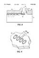
- FIG. 9is a rendering of an SEM photograph of an actual polyimide nozzle array fabricated by the above process.
- the diameter of each nozzle 32is 30 ⁇ while the separation between each nozzle is 10 ⁇ , resulting in a 630 dpi resolution of an image formed on the record medium by this printhead.
- the inter-nozzle separationcan be as little as 5 ⁇ with this process.
Landscapes
- Engineering & Computer Science (AREA)
- Manufacturing & Machinery (AREA)
- Particle Formation And Scattering Control In Inkjet Printers (AREA)
Abstract
Description
Claims (3)
Priority Applications (3)
| Application Number | Priority Date | Filing Date | Title |
|---|---|---|---|
| US08/905,759US6022482A (en) | 1997-08-04 | 1997-08-04 | Monolithic ink jet printhead |
| EP98303779AEP0895865A3 (en) | 1997-08-04 | 1998-05-14 | Monolithic ink jet printhead |
| JP19876198AJP4226691B2 (en) | 1997-08-04 | 1998-07-14 | Monolithic thermal ink jet printhead manufacturing method |
Applications Claiming Priority (1)
| Application Number | Priority Date | Filing Date | Title |
|---|---|---|---|
| US08/905,759US6022482A (en) | 1997-08-04 | 1997-08-04 | Monolithic ink jet printhead |
Publications (1)
| Publication Number | Publication Date |
|---|---|
| US6022482Atrue US6022482A (en) | 2000-02-08 |
Family
ID=25421419
Family Applications (1)
| Application Number | Title | Priority Date | Filing Date |
|---|---|---|---|
| US08/905,759Expired - LifetimeUS6022482A (en) | 1997-08-04 | 1997-08-04 | Monolithic ink jet printhead |
Country Status (3)
| Country | Link |
|---|---|
| US (1) | US6022482A (en) |
| EP (1) | EP0895865A3 (en) |
| JP (1) | JP4226691B2 (en) |
Cited By (37)
| Publication number | Priority date | Publication date | Assignee | Title |
|---|---|---|---|---|
| US6154254A (en)* | 1997-10-15 | 2000-11-28 | Eastman Kodak Company | Electronic camera for producing a digital image having a multimode microfluidic printing device |
| US6245248B1 (en)* | 1998-11-02 | 2001-06-12 | Dbtel Incorporated | Method of aligning a nozzle plate with a mask |
| US6676844B2 (en)* | 2000-12-18 | 2004-01-13 | Samsung Electronics Co. Ltd. | Method for manufacturing ink-jet printhead having hemispherical ink chamber |
| US20040031773A1 (en)* | 1997-07-15 | 2004-02-19 | Silverbrook Research Pty Ltd | Method of fabricating an ink jet printhead |
| US20040035823A1 (en)* | 2002-08-26 | 2004-02-26 | Samsung Electronics Co., Ltd. | Monolithic ink-jet printhead and method of manufacturing the same |
| US20040040929A1 (en)* | 2002-09-04 | 2004-03-04 | Samsung Electronics Co., Ltd. | Monolithic ink-jet printhead and method for manufacturing the same |
| US20050024444A1 (en)* | 2000-04-10 | 2005-02-03 | Olivetti Tecnost S.P.A. | Monolithic printhead with multiple ink feeder channels and relative manufacturing process |
| US6855293B1 (en)* | 1999-03-23 | 2005-02-15 | Hahn-Schickard-Gesellschaft Fuer Angewandte Forschung E.V. | Fluids manipulation device with format conversion |
| US20050099466A1 (en)* | 1998-10-16 | 2005-05-12 | Kia Silverbrook | Printhead wafer with individual ink feed to each nozzle |
| US20050242057A1 (en)* | 2004-04-29 | 2005-11-03 | Hewlett-Packard Developmentcompany, L.P. | Substrate passage formation |
| US20060001703A1 (en)* | 2004-06-30 | 2006-01-05 | Bertelsen Craig M | Die attach methods and apparatus for micro-fluid ejection device |
| US20060037936A1 (en)* | 2004-08-23 | 2006-02-23 | Kim Kyong-Il | Ink jet head including a metal chamber layer and a method of fabricating the same |
| US20060092225A1 (en)* | 2001-10-22 | 2006-05-04 | Seiko Epson Corporation | Apparatus and method of assembling head unit, of positioning liquid droplet ejection head, and of fixing liquid droplet ejection head; as well as method of manufacturing LCD device, organic EL device, electron emission device, PDP device, electrophoretic display device, color filter, organic EL, spacer, metallic wire, lens, resist, and light diffusion member |
| US20060146092A1 (en)* | 2004-12-30 | 2006-07-06 | Barnes Johnathan L | Process for making a micro-fluid ejection head structure |
| US20060219656A1 (en)* | 1998-06-08 | 2006-10-05 | Silverbrook Research Pty Ltd | Method of fabricating printhead IC to have displaceable inkjets |
| US20060238575A1 (en)* | 2002-10-12 | 2006-10-26 | Samsung Electronics Co., Ltd. | Monolithic ink-jet printhead having a metal nozzle plate and manufacturing method thereof |
| US20080074468A1 (en)* | 2000-10-20 | 2008-03-27 | Silverbrook Research Pty Ltd. | Inkjet printhead with nozzle assemblies having raised meniscus-pinning rims |
| US20080136867A1 (en)* | 2006-12-12 | 2008-06-12 | Lebens John A | Liquid ejector having improved chamber walls |
| US20100309252A1 (en)* | 1997-07-15 | 2010-12-09 | Silverbrook Research Pty Ltd | Ejection nozzle arrangement |
| US20110037796A1 (en)* | 1998-10-16 | 2011-02-17 | Silverbrook Research Pty Ltd | Compact nozzle assembly of an inkjet printhead |
| US20110109700A1 (en)* | 1997-07-15 | 2011-05-12 | Silverbrook Research Pty Ltd | Ink ejection mechanism with thermal actuator coil |
| US7950777B2 (en) | 1997-07-15 | 2011-05-31 | Silverbrook Research Pty Ltd | Ejection nozzle assembly |
| US20110134193A1 (en)* | 1997-07-15 | 2011-06-09 | Silverbrook Research Pty Ltd | Nozzle arrangement with an actuator having iris vanes |
| US20110157280A1 (en)* | 1997-07-15 | 2011-06-30 | Silverbrook Research Pty Ltd | Printhead nozzle arrangements with magnetic paddle actuators |
| US20110175970A1 (en)* | 1997-07-15 | 2011-07-21 | Silverbrook Research Pty Ltd | Inkjet printhead integrated circuit incorporating fulcrum assisted ink ejection actuator |
| US20110211025A1 (en)* | 1997-07-15 | 2011-09-01 | Silverbrook Research Pty Ltd | Printhead nozzle having heater of higher resistance than contacts |
| US20110211020A1 (en)* | 1997-07-15 | 2011-09-01 | Silverbrook Research Pty Ltd | Printhead micro-electromechanical nozzle arrangement with motion-transmitting structure |
| US20110228008A1 (en)* | 1997-07-15 | 2011-09-22 | Silverbrook Research Pty Ltd | Printhead having relatively sized fluid ducts and nozzles |
| US8029102B2 (en) | 1997-07-15 | 2011-10-04 | Silverbrook Research Pty Ltd | Printhead having relatively dimensioned ejection ports and arms |
| US8061812B2 (en) | 1997-07-15 | 2011-11-22 | Silverbrook Research Pty Ltd | Ejection nozzle arrangement having dynamic and static structures |
| US20140096385A1 (en)* | 2012-10-10 | 2014-04-10 | Canon Kabushiki Kaisha | Method for producing liquid-ejection head |
| US8869390B2 (en) | 2007-10-01 | 2014-10-28 | Innurvation, Inc. | System and method for manufacturing a swallowable sensor device |
| US9724920B2 (en) | 2013-03-20 | 2017-08-08 | Hewlett-Packard Development Company, L.P. | Molded die slivers with exposed front and back surfaces |
| US10363731B2 (en)* | 2014-12-18 | 2019-07-30 | Palo Alto Research Center Incorporated | Ejector device |
| US10821729B2 (en) | 2013-02-28 | 2020-11-03 | Hewlett-Packard Development Company, L.P. | Transfer molded fluid flow structure |
| US10836169B2 (en) | 2013-02-28 | 2020-11-17 | Hewlett-Packard Development Company, L.P. | Molded printhead |
| US11426900B2 (en) | 2013-02-28 | 2022-08-30 | Hewlett-Packard Development Company, L.P. | Molding a fluid flow structure |
Families Citing this family (5)
| Publication number | Priority date | Publication date | Assignee | Title |
|---|---|---|---|---|
| US6419346B1 (en)* | 2001-01-25 | 2002-07-16 | Hewlett-Packard Company | Two-step trench etch for a fully integrated thermal inkjet printhead |
| KR100510124B1 (en)* | 2002-06-17 | 2005-08-25 | 삼성전자주식회사 | manufacturing method of ink jet print head |
| KR100438726B1 (en)* | 2002-06-25 | 2004-07-05 | 삼성전자주식회사 | Ink jet print head and manufacturing method thereof |
| KR100544209B1 (en)* | 2005-03-24 | 2006-01-23 | 삼성전자주식회사 | Inkjet printhead |
| US7699441B2 (en)* | 2006-12-12 | 2010-04-20 | Eastman Kodak Company | Liquid drop ejector having improved liquid chamber |
Citations (6)
| Publication number | Priority date | Publication date | Assignee | Title |
|---|---|---|---|---|
| US32572A (en)* | 1861-06-18 | Safety-guard for steam-boilers | ||
| US4438191A (en)* | 1982-11-23 | 1984-03-20 | Hewlett-Packard Company | Monolithic ink jet print head |
| US4568953A (en)* | 1982-12-28 | 1986-02-04 | Canon Kabushiki Kaisha | Liquid injection recording apparatus |
| USRE32572E (en) | 1985-04-03 | 1988-01-05 | Xerox Corporation | Thermal ink jet printhead and process therefor |
| US4947192A (en)* | 1988-03-07 | 1990-08-07 | Xerox Corporation | Monolithic silicon integrated circuit chip for a thermal ink jet printer |
| US5211806A (en)* | 1991-12-24 | 1993-05-18 | Xerox Corporation | Monolithic inkjet printhead |
Family Cites Families (3)
| Publication number | Priority date | Publication date | Assignee | Title |
|---|---|---|---|---|
| US5008689A (en)* | 1988-03-16 | 1991-04-16 | Hewlett-Packard Company | Plastic substrate for thermal ink jet printer |
| US6190492B1 (en)* | 1995-10-06 | 2001-02-20 | Lexmark International, Inc. | Direct nozzle plate to chip attachment |
| US5774148A (en)* | 1995-10-19 | 1998-06-30 | Lexmark International, Inc. | Printhead with field oxide as thermal barrier in chip |
- 1997
- 1997-08-04USUS08/905,759patent/US6022482A/ennot_activeExpired - Lifetime
- 1998
- 1998-05-14EPEP98303779Apatent/EP0895865A3/ennot_activeWithdrawn
- 1998-07-14JPJP19876198Apatent/JP4226691B2/ennot_activeExpired - Fee Related
Patent Citations (6)
| Publication number | Priority date | Publication date | Assignee | Title |
|---|---|---|---|---|
| US32572A (en)* | 1861-06-18 | Safety-guard for steam-boilers | ||
| US4438191A (en)* | 1982-11-23 | 1984-03-20 | Hewlett-Packard Company | Monolithic ink jet print head |
| US4568953A (en)* | 1982-12-28 | 1986-02-04 | Canon Kabushiki Kaisha | Liquid injection recording apparatus |
| USRE32572E (en) | 1985-04-03 | 1988-01-05 | Xerox Corporation | Thermal ink jet printhead and process therefor |
| US4947192A (en)* | 1988-03-07 | 1990-08-07 | Xerox Corporation | Monolithic silicon integrated circuit chip for a thermal ink jet printer |
| US5211806A (en)* | 1991-12-24 | 1993-05-18 | Xerox Corporation | Monolithic inkjet printhead |
Non-Patent Citations (2)
| Title |
|---|
| P.F. Man, D. K. Jones, and C. H. Mastrangelo, "Microfluidic Plastic Capillaries on Silicon Substrates: A New Inexpensive Technology for Bioanalysis Chips", Center for Integrated Sensors and Circuits, Department of Electrical Engineering and Computer Science, University of Michigan, Ann Arbor, MI 48109-2212, USA, published on Jan. 26, 1997, in the Proceedings of IEEE 10th Annual International Workshop on Micro Elecro Mechanical Systems, on pp. 311-316. |
| P.F. Man, D. K. Jones, and C. H. Mastrangelo, Microfluidic Plastic Capillaries on Silicon Substrates: A New Inexpensive Technology for Bioanalysis Chips , Center for Integrated Sensors and Circuits, Department of Electrical Engineering and Computer Science, University of Michigan, Ann Arbor, MI 48109 2212, USA, published on Jan. 26, 1997, in the Proceedings of IEEE 10th Annual International Workshop on Micro Elecro Mechanical Systems, on pp. 311 316.* |
Cited By (98)
| Publication number | Priority date | Publication date | Assignee | Title |
|---|---|---|---|---|
| US20110175970A1 (en)* | 1997-07-15 | 2011-07-21 | Silverbrook Research Pty Ltd | Inkjet printhead integrated circuit incorporating fulcrum assisted ink ejection actuator |
| US20110157280A1 (en)* | 1997-07-15 | 2011-06-30 | Silverbrook Research Pty Ltd | Printhead nozzle arrangements with magnetic paddle actuators |
| US8113629B2 (en) | 1997-07-15 | 2012-02-14 | Silverbrook Research Pty Ltd. | Inkjet printhead integrated circuit incorporating fulcrum assisted ink ejection actuator |
| US20040031773A1 (en)* | 1997-07-15 | 2004-02-19 | Silverbrook Research Pty Ltd | Method of fabricating an ink jet printhead |
| US8083326B2 (en) | 1997-07-15 | 2011-12-27 | Silverbrook Research Pty Ltd | Nozzle arrangement with an actuator having iris vanes |
| US8075104B2 (en) | 1997-07-15 | 2011-12-13 | Sliverbrook Research Pty Ltd | Printhead nozzle having heater of higher resistance than contacts |
| US8061812B2 (en) | 1997-07-15 | 2011-11-22 | Silverbrook Research Pty Ltd | Ejection nozzle arrangement having dynamic and static structures |
| US20090273649A1 (en)* | 1997-07-15 | 2009-11-05 | Silverbrook Research Pty Ltd | Inkjet Printhead With Nozzle Layer Defining Etchant Holes |
| US8029102B2 (en) | 1997-07-15 | 2011-10-04 | Silverbrook Research Pty Ltd | Printhead having relatively dimensioned ejection ports and arms |
| US20110134193A1 (en)* | 1997-07-15 | 2011-06-09 | Silverbrook Research Pty Ltd | Nozzle arrangement with an actuator having iris vanes |
| US8025366B2 (en) | 1997-07-15 | 2011-09-27 | Silverbrook Research Pty Ltd | Inkjet printhead with nozzle layer defining etchant holes |
| US20110228008A1 (en)* | 1997-07-15 | 2011-09-22 | Silverbrook Research Pty Ltd | Printhead having relatively sized fluid ducts and nozzles |
| US8020970B2 (en) | 1997-07-15 | 2011-09-20 | Silverbrook Research Pty Ltd | Printhead nozzle arrangements with magnetic paddle actuators |
| US20110211023A1 (en)* | 1997-07-15 | 2011-09-01 | Silverbrook Research Pty Ltd | Printhead ejection nozzle |
| US20110211020A1 (en)* | 1997-07-15 | 2011-09-01 | Silverbrook Research Pty Ltd | Printhead micro-electromechanical nozzle arrangement with motion-transmitting structure |
| US20100309252A1 (en)* | 1997-07-15 | 2010-12-09 | Silverbrook Research Pty Ltd | Ejection nozzle arrangement |
| US20110211025A1 (en)* | 1997-07-15 | 2011-09-01 | Silverbrook Research Pty Ltd | Printhead nozzle having heater of higher resistance than contacts |
| US20080111866A1 (en)* | 1997-07-15 | 2008-05-15 | Silverbrook Research Pty Ltd | Nozzle arrangement with a top wall portion having etchant holes therein |
| US8123336B2 (en) | 1997-07-15 | 2012-02-28 | Silverbrook Research Pty Ltd | Printhead micro-electromechanical nozzle arrangement with motion-transmitting structure |
| US7568791B2 (en) | 1997-07-15 | 2009-08-04 | Silverbrook Research Pty Ltd | Nozzle arrangement with a top wall portion having etchant holes therein |
| US8029101B2 (en) | 1997-07-15 | 2011-10-04 | Silverbrook Research Pty Ltd | Ink ejection mechanism with thermal actuator coil |
| US7950777B2 (en) | 1997-07-15 | 2011-05-31 | Silverbrook Research Pty Ltd | Ejection nozzle assembly |
| US7891779B2 (en) | 1997-07-15 | 2011-02-22 | Silverbrook Research Pty Ltd | Inkjet printhead with nozzle layer defining etchant holes |
| US20110109700A1 (en)* | 1997-07-15 | 2011-05-12 | Silverbrook Research Pty Ltd | Ink ejection mechanism with thermal actuator coil |
| US20110096125A1 (en)* | 1997-07-15 | 2011-04-28 | Silverbrook Research Pty Ltd | Inkjet printhead with nozzle layer defining etchant holes |
| US7347952B2 (en)* | 1997-07-15 | 2008-03-25 | Balmain, New South Wales, Australia | Method of fabricating an ink jet printhead |
| US6154254A (en)* | 1997-10-15 | 2000-11-28 | Eastman Kodak Company | Electronic camera for producing a digital image having a multimode microfluidic printing device |
| US20070034598A1 (en)* | 1998-06-08 | 2007-02-15 | Silverbrook Research Pty Ltd | Method of fabricating a printhead integrated circuit with a nozze chamber in a wafer substrate |
| US20060219656A1 (en)* | 1998-06-08 | 2006-10-05 | Silverbrook Research Pty Ltd | Method of fabricating printhead IC to have displaceable inkjets |
| US7326357B2 (en)* | 1998-06-09 | 2008-02-05 | Silverbrook Research Pty Ltd | Method of fabricating printhead IC to have displaceable inkjets |
| US20080117261A1 (en)* | 1998-06-09 | 2008-05-22 | Silverbrook Research Pty Ltd | Micro-electromechanical nozzle arrangement with non-wicking roof structure for an inkjet printhead |
| US7857426B2 (en) | 1998-06-09 | 2010-12-28 | Silverbrook Research Pty Ltd | Micro-electromechanical nozzle arrangement with a roof structure for minimizing wicking |
| US7413671B2 (en)* | 1998-06-09 | 2008-08-19 | Silverbrook Research Pty Ltd | Method of fabricating a printhead integrated circuit with a nozzle chamber in a wafer substrate |
| US7438391B2 (en) | 1998-06-09 | 2008-10-21 | Silverbrook Research Pty Ltd | Micro-electromechanical nozzle arrangement with non-wicking roof structure for an inkjet printhead |
| US20100277551A1 (en)* | 1998-06-09 | 2010-11-04 | Silverbrook Research Pty Ltd | Micro-electromechanical nozzle arrangement having cantilevered actuator |
| US20080316269A1 (en)* | 1998-06-09 | 2008-12-25 | Silverbrook Research Pty Ltd | Micro-electromechanical nozzle arrangement having cantilevered actuators |
| US7758161B2 (en) | 1998-06-09 | 2010-07-20 | Silverbrook Research Pty Ltd | Micro-electromechanical nozzle arrangement having cantilevered actuators |
| US20090073233A1 (en)* | 1998-06-09 | 2009-03-19 | Silverbrook Research Pty Ltd | Micro-electromechanical nozzle arrangement with a roof structure for minimizing wicking |
| US8061795B2 (en) | 1998-10-16 | 2011-11-22 | Silverbrook Research Pty Ltd | Nozzle assembly of an inkjet printhead |
| US8057014B2 (en) | 1998-10-16 | 2011-11-15 | Silverbrook Research Pty Ltd | Nozzle assembly for an inkjet printhead |
| US20110090288A1 (en)* | 1998-10-16 | 2011-04-21 | Silverbrook Research Pty Ltd | Nozzle assembly of an inkjet printhead |
| US8087757B2 (en) | 1998-10-16 | 2012-01-03 | Silverbrook Research Pty Ltd | Energy control of a nozzle of an inkjet printhead |
| US8066355B2 (en) | 1998-10-16 | 2011-11-29 | Silverbrook Research Pty Ltd | Compact nozzle assembly of an inkjet printhead |
| US7188935B2 (en)* | 1998-10-16 | 2007-03-13 | Silverbrook Research Pty Ltd | Printhead wafer with individual ink feed to each nozzle |
| US20050099466A1 (en)* | 1998-10-16 | 2005-05-12 | Kia Silverbrook | Printhead wafer with individual ink feed to each nozzle |
| US20110037797A1 (en)* | 1998-10-16 | 2011-02-17 | Silverbrook Research Pty Ltd | Control of a nozzle of an inkjet printhead |
| US8047633B2 (en) | 1998-10-16 | 2011-11-01 | Silverbrook Research Pty Ltd | Control of a nozzle of an inkjet printhead |
| US20110037796A1 (en)* | 1998-10-16 | 2011-02-17 | Silverbrook Research Pty Ltd | Compact nozzle assembly of an inkjet printhead |
| US20110037809A1 (en)* | 1998-10-16 | 2011-02-17 | Silverbrook Research Pty Ltd | Nozzle assembly for an inkjet printhead |
| US6245248B1 (en)* | 1998-11-02 | 2001-06-12 | Dbtel Incorporated | Method of aligning a nozzle plate with a mask |
| US6855293B1 (en)* | 1999-03-23 | 2005-02-15 | Hahn-Schickard-Gesellschaft Fuer Angewandte Forschung E.V. | Fluids manipulation device with format conversion |
| US7338580B2 (en)* | 2000-04-10 | 2008-03-04 | Telecom Italia S.P.A. | Monolithic printhead with multiple ink feeder channels and relative manufacturing process |
| US20050024444A1 (en)* | 2000-04-10 | 2005-02-03 | Olivetti Tecnost S.P.A. | Monolithic printhead with multiple ink feeder channels and relative manufacturing process |
| US8029099B2 (en) | 2000-10-20 | 2011-10-04 | Silverbrook Research Pty Ltd | Nozzle assembly with thermal bend actuator for displacing nozzle |
| US20110090287A1 (en)* | 2000-10-20 | 2011-04-21 | Silverbrook Research Pty Ltd | Printhead having ejection nozzles with displaceable fluid chambers |
| US20100149267A1 (en)* | 2000-10-20 | 2010-06-17 | Silverbrook Research Pty Ltd | Nozzle assembly with thermal bend actuator for displacing nozzle |
| US8393715B2 (en) | 2000-10-20 | 2013-03-12 | Zamtec Ltd | Inkjet nozzle assembly having displaceable roof defining ejection port |
| US8091985B2 (en) | 2000-10-20 | 2012-01-10 | Silverbrook Research Pty Ltd | Printhead having ejection nozzles with displaceable fluid chambers |
| US7891769B2 (en)* | 2000-10-20 | 2011-02-22 | Kia Silverbrook | Inkjet printhead with nozzle assemblies having raised meniscus-pinning rims |
| US20080074468A1 (en)* | 2000-10-20 | 2008-03-27 | Silverbrook Research Pty Ltd. | Inkjet printhead with nozzle assemblies having raised meniscus-pinning rims |
| US6676844B2 (en)* | 2000-12-18 | 2004-01-13 | Samsung Electronics Co. Ltd. | Method for manufacturing ink-jet printhead having hemispherical ink chamber |
| US7510272B2 (en)* | 2001-10-22 | 2009-03-31 | Seiko Epson Corporation | Apparatus and method of assembling head unit, of positioning liquid droplet ejection head, and of fixing liquid droplet ejection head; as well as method of manufacturing LCD device, organic EL device, electron emission device, PDP device, electrophoretic display device, color filter, organic EL, spacer, metallic wire, lens, resist, and light diffusion member |
| US20060092225A1 (en)* | 2001-10-22 | 2006-05-04 | Seiko Epson Corporation | Apparatus and method of assembling head unit, of positioning liquid droplet ejection head, and of fixing liquid droplet ejection head; as well as method of manufacturing LCD device, organic EL device, electron emission device, PDP device, electrophoretic display device, color filter, organic EL, spacer, metallic wire, lens, resist, and light diffusion member |
| US7481942B2 (en)* | 2002-08-26 | 2009-01-27 | Samsung Electronics Co., Ltd. | Monolithic ink-jet printhead and method of manufacturing the same |
| US20040035823A1 (en)* | 2002-08-26 | 2004-02-26 | Samsung Electronics Co., Ltd. | Monolithic ink-jet printhead and method of manufacturing the same |
| US20060114294A1 (en)* | 2002-09-04 | 2006-06-01 | Samsung Electronics Co., Ltd. | Monolithic ink-jet printhead and method for manufacturing the same |
| US20040040929A1 (en)* | 2002-09-04 | 2004-03-04 | Samsung Electronics Co., Ltd. | Monolithic ink-jet printhead and method for manufacturing the same |
| US7325310B2 (en) | 2002-09-04 | 2008-02-05 | Samsung Electronics Co., Ltd. | Method for manufacturing a monolithic ink-jet printhead |
| US20060238575A1 (en)* | 2002-10-12 | 2006-10-26 | Samsung Electronics Co., Ltd. | Monolithic ink-jet printhead having a metal nozzle plate and manufacturing method thereof |
| US20050242057A1 (en)* | 2004-04-29 | 2005-11-03 | Hewlett-Packard Developmentcompany, L.P. | Substrate passage formation |
| US7429335B2 (en) | 2004-04-29 | 2008-09-30 | Shen Buswell | Substrate passage formation |
| US20060001703A1 (en)* | 2004-06-30 | 2006-01-05 | Bertelsen Craig M | Die attach methods and apparatus for micro-fluid ejection device |
| US7311386B2 (en)* | 2004-06-30 | 2007-12-25 | Lexmark Interntional, Inc. | Die attach methods and apparatus for micro-fluid ejection device |
| US20060037936A1 (en)* | 2004-08-23 | 2006-02-23 | Kim Kyong-Il | Ink jet head including a metal chamber layer and a method of fabricating the same |
| US7465403B2 (en) | 2004-08-23 | 2008-12-16 | Samsung Electronics Co., Ltd. | Ink jet head including a metal chamber layer and a method of fabricating the same |
| US20070222820A1 (en)* | 2004-12-30 | 2007-09-27 | Barnes Johnathan L | Micro-fluid ejection head structure |
| US20060146092A1 (en)* | 2004-12-30 | 2006-07-06 | Barnes Johnathan L | Process for making a micro-fluid ejection head structure |
| US7254890B2 (en)* | 2004-12-30 | 2007-08-14 | Lexmark International, Inc. | Method of making a microfluid ejection head structure |
| US7600858B2 (en) | 2004-12-30 | 2009-10-13 | Lexmark International, Inc. | Micro-fluid ejection head structure |
| US7600856B2 (en) | 2006-12-12 | 2009-10-13 | Eastman Kodak Company | Liquid ejector having improved chamber walls |
| US20080136867A1 (en)* | 2006-12-12 | 2008-06-12 | Lebens John A | Liquid ejector having improved chamber walls |
| US9730336B2 (en) | 2007-10-01 | 2017-08-08 | Innurvation, Inc. | System for manufacturing a swallowable sensor device |
| US8869390B2 (en) | 2007-10-01 | 2014-10-28 | Innurvation, Inc. | System and method for manufacturing a swallowable sensor device |
| US20140096385A1 (en)* | 2012-10-10 | 2014-04-10 | Canon Kabushiki Kaisha | Method for producing liquid-ejection head |
| US9139003B2 (en)* | 2012-10-10 | 2015-09-22 | Canon Kabushiki Kaisha | Method for producing liquid-ejection head |
| US10836169B2 (en) | 2013-02-28 | 2020-11-17 | Hewlett-Packard Development Company, L.P. | Molded printhead |
| US10821729B2 (en) | 2013-02-28 | 2020-11-03 | Hewlett-Packard Development Company, L.P. | Transfer molded fluid flow structure |
| US10994539B2 (en) | 2013-02-28 | 2021-05-04 | Hewlett-Packard Development Company, L.P. | Fluid flow structure forming method |
| US11130339B2 (en) | 2013-02-28 | 2021-09-28 | Hewlett-Packard Development Company, L.P. | Molded fluid flow structure |
| US11426900B2 (en) | 2013-02-28 | 2022-08-30 | Hewlett-Packard Development Company, L.P. | Molding a fluid flow structure |
| US11541659B2 (en) | 2013-02-28 | 2023-01-03 | Hewlett-Packard Development Company, L.P. | Molded printhead |
| US10500859B2 (en) | 2013-03-20 | 2019-12-10 | Hewlett-Packard Development Company, L.P. | Molded die slivers with exposed front and back surfaces |
| US9724920B2 (en) | 2013-03-20 | 2017-08-08 | Hewlett-Packard Development Company, L.P. | Molded die slivers with exposed front and back surfaces |
| US11292257B2 (en) | 2013-03-20 | 2022-04-05 | Hewlett-Packard Development Company, L.P. | Molded die slivers with exposed front and back surfaces |
| US10081186B2 (en) | 2014-03-18 | 2018-09-25 | Hewlett-Packard Development Company, L.P. | Molded die slivers with exposed front and back surfaces |
| US10363731B2 (en)* | 2014-12-18 | 2019-07-30 | Palo Alto Research Center Incorporated | Ejector device |
| US10981374B2 (en) | 2014-12-18 | 2021-04-20 | Palo Alto Research Center Incorporated | Ejector device |
| US11465401B2 (en) | 2014-12-18 | 2022-10-11 | Palo Alto Research Center Incoporated | Ejector device |
Also Published As
| Publication number | Publication date |
|---|---|
| JP4226691B2 (en) | 2009-02-18 |
| EP0895865A2 (en) | 1999-02-10 |
| JPH1170661A (en) | 1999-03-16 |
| EP0895865A3 (en) | 2000-05-03 |
Similar Documents
| Publication | Publication Date | Title |
|---|---|---|
| US6022482A (en) | Monolithic ink jet printhead | |
| JP3213624B2 (en) | Print head | |
| US6137443A (en) | Single-side fabrication process for forming inkjet monolithic printing element array on a substrate | |
| US6679587B2 (en) | Fluid ejection device with a composite substrate | |
| JPS6280054A (en) | Ink jet type printing head with built-in filter and manufacture thereof | |
| JP2001071504A (en) | Printer having ink jet print head, manufacture thereof and method for printing | |
| US20020097302A1 (en) | Two-step trench etch for a fully integrated themal inkjet printhead | |
| JPH02235642A (en) | Large monolithic thermal ink jet printing head | |
| JP2001071502A (en) | Printer having ink jet print head, manufacture thereof and method for printing | |
| CN100480047C (en) | Ink-jetting printing head with nozzle assembly array | |
| JP2001071503A (en) | Printer having ink jet print head, manufacture thereof and method for printing | |
| US6079819A (en) | Ink jet printhead having a low cross talk ink channel structure | |
| US6186616B1 (en) | Ink jet head having an improved orifice plate, a method for manufacturing such ink jet heads, and an ink jet apparatus provided with such ink jet head | |
| JP2002192723A (en) | Printer, method for forming the same, and printing method | |
| JP2002283580A (en) | Ink supply trench etching technique for completely integrated thermal ink-jet printing head | |
| US6776915B2 (en) | Method of manufacturing a fluid ejection device with a fluid channel therethrough | |
| US20050001884A1 (en) | Fluid injection micro device and fabrication method thereof | |
| JP2001130009A (en) | Method of manufacturing ink jet printer head | |
| US6183069B1 (en) | Ink jet printhead having a patternable ink channel structure | |
| CN101287605B (en) | Low-consumption electrode connection for ink-jet printhead | |
| JP3799871B2 (en) | Inkjet printer head manufacturing method | |
| JP4606772B2 (en) | Side-ejecting droplet ejector and method for manufacturing side-ejecting droplet ejector | |
| JPH05124208A (en) | Liquid jet recording head manufacturing method and liquid jet recording head | |
| US8567912B2 (en) | Inkjet printing device with composite substrate | |
| KR100421027B1 (en) | Inkjet printhead and manufacturing method thereof |
Legal Events
| Date | Code | Title | Description |
|---|---|---|---|
| AS | Assignment | Owner name:XEROX CORPORATION, CONNECTICUT Free format text:ASSIGNMENT OF ASSIGNORS INTEREST;ASSIGNORS:CHEN, JINGKUANG;HSEIH, BIAY-CHENG;REEL/FRAME:008733/0872 Effective date:19970729 | |
| STCF | Information on status: patent grant | Free format text:PATENTED CASE | |
| AS | Assignment | Owner name:BANK ONE, NA, AS ADMINISTRATIVE AGENT, ILLINOIS Free format text:SECURITY INTEREST;ASSIGNOR:XEROX CORPORATION;REEL/FRAME:013153/0001 Effective date:20020621 | |
| FPAY | Fee payment | Year of fee payment:4 | |
| AS | Assignment | Owner name:JPMORGAN CHASE BANK, AS COLLATERAL AGENT, TEXAS Free format text:SECURITY AGREEMENT;ASSIGNOR:XEROX CORPORATION;REEL/FRAME:015134/0476 Effective date:20030625 Owner name:JPMORGAN CHASE BANK, AS COLLATERAL AGENT,TEXAS Free format text:SECURITY AGREEMENT;ASSIGNOR:XEROX CORPORATION;REEL/FRAME:015134/0476 Effective date:20030625 | |
| FPAY | Fee payment | Year of fee payment:8 | |
| FPAY | Fee payment | Year of fee payment:12 | |
| AS | Assignment | Owner name:XEROX CORPORATION, CONNECTICUT Free format text:RELEASE BY SECURED PARTY;ASSIGNOR:JPMORGAN CHASE BANK, N.A. AS SUCCESSOR-IN-INTEREST ADMINISTRATIVE AGENT AND COLLATERAL AGENT TO JPMORGAN CHASE BANK;REEL/FRAME:066728/0193 Effective date:20220822 |