US6018538A - High speed non-biased semiconductor laser dione driver for high speed digital communication - Google Patents
High speed non-biased semiconductor laser dione driver for high speed digital communicationDownload PDFInfo
- Publication number
- US6018538A US6018538AUS08/877,910US87791097AUS6018538AUS 6018538 AUS6018538 AUS 6018538AUS 87791097 AUS87791097 AUS 87791097AUS 6018538 AUS6018538 AUS 6018538A
- Authority
- US
- United States
- Prior art keywords
- laser diode
- semiconductor laser
- driving
- high speed
- mos transistor
- Prior art date
- Legal status (The legal status is an assumption and is not a legal conclusion. Google has not performed a legal analysis and makes no representation as to the accuracy of the status listed.)
- Expired - Lifetime
Links
- 239000004065semiconductorSubstances0.000titleclaimsdescription32
- 230000003287optical effectEffects0.000claimsabstractdescription12
- 239000003990capacitorSubstances0.000claimsdescription6
- 238000000034methodMethods0.000claimsdescription6
- 230000000737periodic effectEffects0.000claims4
- 238000005286illuminationMethods0.000claims1
- 230000005540biological transmissionEffects0.000description1
- 230000000694effectsEffects0.000description1
- 230000006798recombinationEffects0.000description1
- 238000005215recombinationMethods0.000description1
- 230000007704transitionEffects0.000description1
- 238000011144upstream manufacturingMethods0.000description1
Images

Classifications
- H—ELECTRICITY
- H03—ELECTRONIC CIRCUITRY
- H03K—PULSE TECHNIQUE
- H03K17/00—Electronic switching or gating, i.e. not by contact-making and –breaking
- H03K17/04—Modifications for accelerating switching
- H03K17/041—Modifications for accelerating switching without feedback from the output circuit to the control circuit
- H03K17/04106—Modifications for accelerating switching without feedback from the output circuit to the control circuit in field-effect transistor switches
- H—ELECTRICITY
- H01—ELECTRIC ELEMENTS
- H01S—DEVICES USING THE PROCESS OF LIGHT AMPLIFICATION BY STIMULATED EMISSION OF RADIATION [LASER] TO AMPLIFY OR GENERATE LIGHT; DEVICES USING STIMULATED EMISSION OF ELECTROMAGNETIC RADIATION IN WAVE RANGES OTHER THAN OPTICAL
- H01S5/00—Semiconductor lasers
- H01S5/04—Processes or apparatus for excitation, e.g. pumping, e.g. by electron beams
- H01S5/042—Electrical excitation ; Circuits therefor
Definitions
- This inventionrelates to optical communication, and more particularly, to a circuit for driving a semiconductor laser diode used in an optical communications link.
- H-PONhigh speed passive optical networks
- no DC optical signalis allowed in the upstream from the optical network unit (ONU) on the customer premises to the optical line terminal (OLT) located in the central office.
- OLToptical line terminal
- the tail emissionis caused by 1) electrical charge that is stored in the laser diode while it is being driven and 2) the fact that the process of recombination of the charges in the laser diode is a slow one even after the driving current is removed.
- the tailextends over 100 ns.
- the signal packets from the different customer premises ONUsoften wind up being spaced much closer together than the length of the tail. This implies that a packet from a particular customer premises ONU is influenced by the tail that was generated by the customer premises ONU which was transmitting a packet in the time slot immediately precedent to that of the particular customer premises ONU.
- the laser diode driverincludes an energy drainage path that is activated when packet communication is over.
- the terminals of the laser diodeare short-circuited to provide the energy drainage path.
- the laser diodeis reverse biased, so that charges stored in the laser diode are combined with charges which are provided thereto.
- the tail emissionis substantially eliminated.
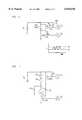
- FIG. 1shows an example of a tail that results when a semiconductor laser diode is operated without bias in the prior art, because the optical output does not turn off immediately after the driving signal is turned off;
- FIG. 2shows a simple prior art arrangement for driving a laser diode without bias
- FIG. 3shows an exemplary arrangement for driving a laser diode but having an energy drainage path in accordance with the principles of the invention.
- FIG. 4shows another embodiment of the invention that further accelerates the energy drainage process of the laser diode, albeit at the cost of additional components.
- FIG. 2shows a simple prior art arrangement for driving laser diode (LD) 205 without bias.
- n-MOS 201 transistoroperates as a switch. When the signal to gate 203 is high, n-MOS transistor 201 becomes conductive and a current passes through laser diode 205, causing emission of a laser beam. However, when n-MOS transistor 201 is turned off, by having the signal to gate 203 (S) be low, the stored energy in laser diode 205 has no path to drain out. Therefore, this stored energy is slowly discharged within the laser diode, and it is this slow discharge that causes the prior art tail.
- Ssignal to gate 203
- FIG. 3adds an energy drainage path in accordance with the principles of the invention. Underlying the circuit of FIG. 3 is the circuit of FIG. 2. However, p-MOS transistor 307 and pull-up resistor 309 have been added to the circuit.
- gate 311 of p-MOS transistor 307is normally set high by pull-up resistor 303. This results in p-MOS transistor 307 being in the off state.
- laser diode 205is activated when n-MOS transistor 201 is turned on by gate signal S being high.
- a pulse of "LOW"is applied to gate 311 of p-MOS transistor 307. This pulse makes p-MOS transistor 307 conductive i.e., in the on-state.
- n-MOS transistor 201is in the off-state. Therefore, the terminals of laser diode 205 are short-circuited together and an energy drainage path for the laser diode is formed.
- the length of the laser emission tailis shortened.
- FIG. 4shows another embodiment of the invention that further accelerates the energy drainage process, albeit at the cost of additional components. More specifically, diodes 421 and 423, as well as capacitor 425 are added to the circuit shown in FIG. 3. Diodes 421 and 423 are high current rectifier diodes. When signal S1 is high, current passes through diodes 421 and 423, laser diode (LD) 201, and n-MOS transistor 201. The potential at point A is V 0 -2V th , where V th is the forward threshold of diodes 421 and 423. Usually, V th is about 0.7V in a Si rectifier diode. This potential V 0 -2V th is stored in capacitor 425.
- V 0 -2V this the forward threshold of diodes 421 and 423.
- n-MOS transistor 201is turned off and p-MOS transistor 307 is turned on, by bringing the signal S2 at gate 311 thereof low, laser diode 205 is back-biased by 2V th , and reverse current is supplied from capacitor 425 and voltage source V 0 .
- this circuitsubstantially eliminates the tail emission.
- the use of two diodesis simply an exemplary way of achieving a voltage drop so that a reverse bias effect results at the laser diode.
- any technique of achieving a voltage dropmay be employed, including, but not limited to a resistor, a zener diode, or the like.
- the components for achieving the voltage dropshould be selected, preferably, to yield the greatest voltage drop achievable while consuming the least current in the laser diode active state.
- n-MOS and p-MOS transistorsare strictly exemplary, those of ordinary skill in the art will readily recognize how to change the types of transistors employed. Furthermore, those of ordinary skill in the art will recognize that it is not necessary to employ opposite types of transistors to implement the invention, but instead, the invention may be implemented using a single type of transistor.
- the tails that are generated after each one to zero transition by a single ONUare easily ignored, because the tail power, although a function of the particular laser diode, is typically no more than 10% of the laser diode output power.
- the laser diode output power between different ONUsis permitted to vary by a very large amount, e.g., the maximum power may be up to 1000 times greater than the minimum power, the tail from a laser diode which was generating the maximum power will easily dwarf the signal from the laser diode of the next ONU which is generating only the minimum power.
Landscapes
- Physics & Mathematics (AREA)
- Condensed Matter Physics & Semiconductors (AREA)
- General Physics & Mathematics (AREA)
- Electromagnetism (AREA)
- Optics & Photonics (AREA)
- Semiconductor Lasers (AREA)
- Optical Communication System (AREA)
Abstract
Description
Claims (12)
Priority Applications (5)
| Application Number | Priority Date | Filing Date | Title |
|---|---|---|---|
| US08/877,910US6018538A (en) | 1997-06-18 | 1997-06-18 | High speed non-biased semiconductor laser dione driver for high speed digital communication |
| CA002237506ACA2237506A1 (en) | 1997-06-18 | 1998-05-13 | High speed non-biased semiconductor laser diode driver for high speed digital communication |
| EP98304537AEP0886350B1 (en) | 1997-06-18 | 1998-06-09 | High speed non-biased semiconductor laser diode driver for high speed digital communication |
| DE69818352TDE69818352T2 (en) | 1997-06-18 | 1998-06-09 | High-speed driver for non-polarized semiconductor diode lasers in high-speed digital transmission |
| JP17043498AJP3588254B2 (en) | 1997-06-18 | 1998-06-18 | High-speed bias-free semiconductor laser diode drive circuit for high-speed digital communication |
Applications Claiming Priority (1)
| Application Number | Priority Date | Filing Date | Title |
|---|---|---|---|
| US08/877,910US6018538A (en) | 1997-06-18 | 1997-06-18 | High speed non-biased semiconductor laser dione driver for high speed digital communication |
Publications (1)
| Publication Number | Publication Date |
|---|---|
| US6018538Atrue US6018538A (en) | 2000-01-25 |
Family
ID=25370976
Family Applications (1)
| Application Number | Title | Priority Date | Filing Date |
|---|---|---|---|
| US08/877,910Expired - LifetimeUS6018538A (en) | 1997-06-18 | 1997-06-18 | High speed non-biased semiconductor laser dione driver for high speed digital communication |
Country Status (5)
| Country | Link |
|---|---|
| US (1) | US6018538A (en) |
| EP (1) | EP0886350B1 (en) |
| JP (1) | JP3588254B2 (en) |
| CA (1) | CA2237506A1 (en) |
| DE (1) | DE69818352T2 (en) |
Cited By (4)
| Publication number | Priority date | Publication date | Assignee | Title |
|---|---|---|---|---|
| US6859624B1 (en) | 2000-11-17 | 2005-02-22 | Alloptic, Inc. | Laser diode optical transmitter for TDMA system with fast enable and disable times |
| US20050245998A1 (en)* | 2004-04-30 | 2005-11-03 | Led Healing Light, Llc | Hand held pulse laser for therapeutic use |
| US20090180500A1 (en)* | 2007-10-23 | 2009-07-16 | Ipg Photonics Corporation | Method and device for controlling optical output of laser diode |
| US11482836B2 (en)* | 2020-01-28 | 2022-10-25 | Stmicroelectronics (Grenoble 2) Sas | Laser diode driver circuits and methods of operating thereof |
Families Citing this family (5)
| Publication number | Priority date | Publication date | Assignee | Title |
|---|---|---|---|---|
| DE10320333B4 (en)* | 2003-05-06 | 2009-06-18 | Infineon Technologies Ag | Electrical circuits for a directly modulated semiconductor radiation source |
| DE202006005148U1 (en)* | 2006-03-29 | 2007-08-09 | Ic-Haus Gmbh | Circuit arrangement for generating fast laser pulses |
| JP5509537B2 (en)* | 2008-04-16 | 2014-06-04 | セイコーエプソン株式会社 | Projector and driving method thereof |
| JP5509662B2 (en)* | 2009-04-13 | 2014-06-04 | ソニー株式会社 | Laser drive device |
| US9185762B2 (en) | 2013-04-19 | 2015-11-10 | Infineon Technologies Ag | Time of flight illumination circuit |
Citations (11)
| Publication number | Priority date | Publication date | Assignee | Title |
|---|---|---|---|---|
| DE3711051A1 (en)* | 1986-04-03 | 1987-10-29 | Copal Electronics | DRIVER AND CONTROL CIRCUIT FOR LASER DIODES |
| EP0312143A1 (en)* | 1987-10-14 | 1989-04-19 | Koninklijke Philips Electronics N.V. | Magneto-optical recording apparatus and energizing circuit for use in such a magneto-optical recording apparatus |
| US4924473A (en)* | 1989-03-28 | 1990-05-08 | Raynet Corporation | Laser diode protection circuit |
| US5140175A (en)* | 1989-06-24 | 1992-08-18 | Mitsubishi Rayon Co., Ltd. | Light-emitting diode drive circuit with fast rise time and fall time |
| US5349595A (en)* | 1992-02-28 | 1994-09-20 | Canon Kabushiki Kaisha | Drive circuit for semiconductor light-emitting device |
| US5513197A (en)* | 1992-11-12 | 1996-04-30 | Matsushita Electric Industrial Co., Ltd. | Semiconductor laser drive circuit including switched current source |
| US5598040A (en)* | 1995-05-31 | 1997-01-28 | Eastman Kodak Company | Laser writer having high speed high current laser driver |
| US5602665A (en)* | 1994-12-06 | 1997-02-11 | Nec Corporation | Optical transmitting/receiving apparatus for bidirectional communication systems |
| US5631917A (en)* | 1995-02-23 | 1997-05-20 | Miyachi Technos Corporation | Laser apparatus |
| US5651017A (en)* | 1995-04-21 | 1997-07-22 | Xerox Corporation | Drive circuit for high-speed modulation of a laser diode |
| US5675599A (en)* | 1992-09-24 | 1997-10-07 | Hitachi, Ltd. | Driving circuit of laser diode and optical transmission device |
- 1997
- 1997-06-18USUS08/877,910patent/US6018538A/ennot_activeExpired - Lifetime
- 1998
- 1998-05-13CACA002237506Apatent/CA2237506A1/ennot_activeAbandoned
- 1998-06-09EPEP98304537Apatent/EP0886350B1/ennot_activeExpired - Lifetime
- 1998-06-09DEDE69818352Tpatent/DE69818352T2/ennot_activeExpired - Lifetime
- 1998-06-18JPJP17043498Apatent/JP3588254B2/ennot_activeExpired - Fee Related
Patent Citations (11)
| Publication number | Priority date | Publication date | Assignee | Title |
|---|---|---|---|---|
| DE3711051A1 (en)* | 1986-04-03 | 1987-10-29 | Copal Electronics | DRIVER AND CONTROL CIRCUIT FOR LASER DIODES |
| EP0312143A1 (en)* | 1987-10-14 | 1989-04-19 | Koninklijke Philips Electronics N.V. | Magneto-optical recording apparatus and energizing circuit for use in such a magneto-optical recording apparatus |
| US4924473A (en)* | 1989-03-28 | 1990-05-08 | Raynet Corporation | Laser diode protection circuit |
| US5140175A (en)* | 1989-06-24 | 1992-08-18 | Mitsubishi Rayon Co., Ltd. | Light-emitting diode drive circuit with fast rise time and fall time |
| US5349595A (en)* | 1992-02-28 | 1994-09-20 | Canon Kabushiki Kaisha | Drive circuit for semiconductor light-emitting device |
| US5675599A (en)* | 1992-09-24 | 1997-10-07 | Hitachi, Ltd. | Driving circuit of laser diode and optical transmission device |
| US5513197A (en)* | 1992-11-12 | 1996-04-30 | Matsushita Electric Industrial Co., Ltd. | Semiconductor laser drive circuit including switched current source |
| US5602665A (en)* | 1994-12-06 | 1997-02-11 | Nec Corporation | Optical transmitting/receiving apparatus for bidirectional communication systems |
| US5631917A (en)* | 1995-02-23 | 1997-05-20 | Miyachi Technos Corporation | Laser apparatus |
| US5651017A (en)* | 1995-04-21 | 1997-07-22 | Xerox Corporation | Drive circuit for high-speed modulation of a laser diode |
| US5598040A (en)* | 1995-05-31 | 1997-01-28 | Eastman Kodak Company | Laser writer having high speed high current laser driver |
Non-Patent Citations (8)
| Title |
|---|
| European Search Report No. EP 98 30 4537, Sep. 25, 1998 European Patent Office The Hague.* |
| European Search Report No. EP 98 30 4537, Sep. 25, 1998--European Patent Office--The Hague. |
| Howard, L. and Daneshvar, K: "Nonosecond-Pulse Generator For Laser Diodes"--Review of Scientific Instruments 60, No. 10, New York, Oct. 1989, pp. 3343-3345. |
| Howard, L. and Daneshvar, K: Nonosecond Pulse Generator For Laser Diodes Review of Scientific Instruments 60, No. 10, New York, Oct. 1989, pp. 3343 3345.* |
| Uenohara, H.: Kawamura, Y; Iwamura, H: "Long-Wavelength Multiple-Quantum-Well Voltage-Controlled Bistable Laser Diodes"--IEEE Journal of Quantum Electronics, Dec. 31, 1995, No. 12, New York, pp. 2142-2147. |
| Uenohara, H.: Kawamura, Y; Iwamura, H: Long Wavelength Multiple Quantum Well Voltage Controlled Bistable Laser Diodes IEEE Journal of Quantum Electronics, Dec. 31, 1995, No. 12, New York, pp. 2142 2147.* |
| Wedding, B: "Reduction of Bit Error Rate in High Speed Optical Transmission Systems Due to Optimized Electrical Drive Pulse Shaping"--European Conference on Optical Communication, Sep. 11-15, 1998, vol. Part 1, No. Conf. 14. Sep. 11, 1998, pp. 187-190, XP000145107--Institution of Electrical Engineer, p. 187, line 5-line 34; figure 1B. |
| Wedding, B: Reduction of Bit Error Rate in High Speed Optical Transmission Systems Due to Optimized Electrical Drive Pulse Shaping European Conference on Optical Communication, Sep. 11 15, 1998, vol. Part 1, No. Conf. 14. Sep. 11, 1998, pp. 187 190, XP000145107 Institution of Electrical Engineer, p. 187, line 5 line 34; figure 1B.* |
Cited By (6)
| Publication number | Priority date | Publication date | Assignee | Title |
|---|---|---|---|---|
| US6859624B1 (en) | 2000-11-17 | 2005-02-22 | Alloptic, Inc. | Laser diode optical transmitter for TDMA system with fast enable and disable times |
| US20050245998A1 (en)* | 2004-04-30 | 2005-11-03 | Led Healing Light, Llc | Hand held pulse laser for therapeutic use |
| US20090180500A1 (en)* | 2007-10-23 | 2009-07-16 | Ipg Photonics Corporation | Method and device for controlling optical output of laser diode |
| US7873085B2 (en)* | 2007-10-23 | 2011-01-18 | Andrei Babushkin | Method and device for controlling optical output of laser diode |
| US11482836B2 (en)* | 2020-01-28 | 2022-10-25 | Stmicroelectronics (Grenoble 2) Sas | Laser diode driver circuits and methods of operating thereof |
| US12388233B2 (en) | 2020-01-28 | 2025-08-12 | Stmicroelectronics (Grenoble 2) Sas | Laser diode driver circuits and methods of operating thereof |
Also Published As
| Publication number | Publication date |
|---|---|
| DE69818352D1 (en) | 2003-10-30 |
| JPH1174623A (en) | 1999-03-16 |
| EP0886350B1 (en) | 2003-09-24 |
| DE69818352T2 (en) | 2004-07-08 |
| JP3588254B2 (en) | 2004-11-10 |
| CA2237506A1 (en) | 1998-12-18 |
| EP0886350A1 (en) | 1998-12-23 |
Similar Documents
| Publication | Publication Date | Title |
|---|---|---|
| US5329210A (en) | High-speed driver for an LED communication system or the like | |
| US6242870B1 (en) | Light emitting device driving circuit | |
| US4571506A (en) | LED Driver Circuit | |
| US6018538A (en) | High speed non-biased semiconductor laser dione driver for high speed digital communication | |
| EP0905900B1 (en) | Driving circuit for light emitting diode | |
| US8139903B2 (en) | Driving circuit of optical gate switch | |
| US20020085599A1 (en) | Electronic driver circuit for directly modulated semiconductor lasers | |
| EP0597644A1 (en) | Semiconductor laser driving circuit | |
| KR102797771B1 (en) | GaN laser diode driving FET using gate current reuse | |
| JP5130975B2 (en) | Optical switch drive circuit | |
| US6778569B2 (en) | Optical source driver with improved input stage | |
| US12040837B2 (en) | Laser emitting system | |
| US6516015B1 (en) | Laser driver and optical transceiver | |
| JP3482165B2 (en) | Laser drive circuit and optical transmitter / receiver | |
| US7483460B2 (en) | Transmitter optical subassembly and a transmitter optical module installing the same | |
| JP3098621B2 (en) | Light emitting element drive circuit | |
| US7280574B1 (en) | Circuit for driving a laser diode and method | |
| JP2004356702A (en) | Optical semiconductor relay | |
| JP2010114462A (en) | System for controlling electric current quantity | |
| JP2771163B2 (en) | LED drive circuit | |
| Chen et al. | 4 Gbit/s GaAs MESFET laser-driver IC | |
| JP3126048B2 (en) | Optical transceiver circuit | |
| US20020110167A1 (en) | Modulators for vertical cavity surface emitting lasers | |
| Suzuki et al. | High-speed 1.3-µm LED transmitter using GaAs driver IC | |
| JP2005020192A (en) | Optical transmitter |
Legal Events
| Date | Code | Title | Description |
|---|---|---|---|
| AS | Assignment | Owner name:LUCENT TECHNOLOGIES, INC., NEW JERSEY Free format text:ASSIGNMENT OF ASSIGNORS INTEREST;ASSIGNOR:OTA, YUSUKE;REEL/FRAME:008607/0049 Effective date:19970617 | |
| FEPP | Fee payment procedure | Free format text:PAYOR NUMBER ASSIGNED (ORIGINAL EVENT CODE: ASPN); ENTITY STATUS OF PATENT OWNER: LARGE ENTITY | |
| STCF | Information on status: patent grant | Free format text:PATENTED CASE | |
| FEPP | Fee payment procedure | Free format text:PAYOR NUMBER ASSIGNED (ORIGINAL EVENT CODE: ASPN); ENTITY STATUS OF PATENT OWNER: LARGE ENTITY Free format text:PAYER NUMBER DE-ASSIGNED (ORIGINAL EVENT CODE: RMPN); ENTITY STATUS OF PATENT OWNER: LARGE ENTITY | |
| FPAY | Fee payment | Year of fee payment:4 | |
| FPAY | Fee payment | Year of fee payment:8 | |
| FPAY | Fee payment | Year of fee payment:12 | |
| AS | Assignment | Owner name:DEUTSCHE BANK AG NEW YORK BRANCH, AS COLLATERAL AG Free format text:PATENT SECURITY AGREEMENT;ASSIGNORS:LSI CORPORATION;AGERE SYSTEMS LLC;REEL/FRAME:032856/0031 Effective date:20140506 | |
| AS | Assignment | Owner name:AVAGO TECHNOLOGIES GENERAL IP (SINGAPORE) PTE. LTD Free format text:ASSIGNMENT OF ASSIGNORS INTEREST;ASSIGNOR:AGERE SYSTEMS LLC;REEL/FRAME:035365/0634 Effective date:20140804 | |
| AS | Assignment | Owner name:LSI CORPORATION, CALIFORNIA Free format text:TERMINATION AND RELEASE OF SECURITY INTEREST IN PATENT RIGHTS (RELEASES RF 032856-0031);ASSIGNOR:DEUTSCHE BANK AG NEW YORK BRANCH, AS COLLATERAL AGENT;REEL/FRAME:037684/0039 Effective date:20160201 Owner name:AGERE SYSTEMS LLC, PENNSYLVANIA Free format text:TERMINATION AND RELEASE OF SECURITY INTEREST IN PATENT RIGHTS (RELEASES RF 032856-0031);ASSIGNOR:DEUTSCHE BANK AG NEW YORK BRANCH, AS COLLATERAL AGENT;REEL/FRAME:037684/0039 Effective date:20160201 | |
| AS | Assignment | Owner name:BANK OF AMERICA, N.A., AS COLLATERAL AGENT, NORTH CAROLINA Free format text:PATENT SECURITY AGREEMENT;ASSIGNOR:AVAGO TECHNOLOGIES GENERAL IP (SINGAPORE) PTE. LTD.;REEL/FRAME:037808/0001 Effective date:20160201 Owner name:BANK OF AMERICA, N.A., AS COLLATERAL AGENT, NORTH Free format text:PATENT SECURITY AGREEMENT;ASSIGNOR:AVAGO TECHNOLOGIES GENERAL IP (SINGAPORE) PTE. LTD.;REEL/FRAME:037808/0001 Effective date:20160201 | |
| AS | Assignment | Owner name:AVAGO TECHNOLOGIES GENERAL IP (SINGAPORE) PTE. LTD., SINGAPORE Free format text:TERMINATION AND RELEASE OF SECURITY INTEREST IN PATENTS;ASSIGNOR:BANK OF AMERICA, N.A., AS COLLATERAL AGENT;REEL/FRAME:041710/0001 Effective date:20170119 Owner name:AVAGO TECHNOLOGIES GENERAL IP (SINGAPORE) PTE. LTD Free format text:TERMINATION AND RELEASE OF SECURITY INTEREST IN PATENTS;ASSIGNOR:BANK OF AMERICA, N.A., AS COLLATERAL AGENT;REEL/FRAME:041710/0001 Effective date:20170119 |