US6016357A - Feedback method to repair phase shift masks - Google Patents
Feedback method to repair phase shift masksDownload PDFInfo
- Publication number
- US6016357A US6016357AUS08/876,931US87693197AUS6016357AUS 6016357 AUS6016357 AUS 6016357AUS 87693197 AUS87693197 AUS 87693197AUS 6016357 AUS6016357 AUS 6016357A
- Authority
- US
- United States
- Prior art keywords
- mask
- aerial image
- defect
- parameters
- patch
- Prior art date
- Legal status (The legal status is an assumption and is not a legal conclusion. Google has not performed a legal analysis and makes no representation as to the accuracy of the status listed.)
- Expired - Lifetime
Links
Images


Classifications
- G—PHYSICS
- G03—PHOTOGRAPHY; CINEMATOGRAPHY; ANALOGOUS TECHNIQUES USING WAVES OTHER THAN OPTICAL WAVES; ELECTROGRAPHY; HOLOGRAPHY
- G03F—PHOTOMECHANICAL PRODUCTION OF TEXTURED OR PATTERNED SURFACES, e.g. FOR PRINTING, FOR PROCESSING OF SEMICONDUCTOR DEVICES; MATERIALS THEREFOR; ORIGINALS THEREFOR; APPARATUS SPECIALLY ADAPTED THEREFOR
- G03F1/00—Originals for photomechanical production of textured or patterned surfaces, e.g., masks, photo-masks, reticles; Mask blanks or pellicles therefor; Containers specially adapted therefor; Preparation thereof
- G03F1/68—Preparation processes not covered by groups G03F1/20 - G03F1/50
- G03F1/72—Repair or correction of mask defects
- G—PHYSICS
- G03—PHOTOGRAPHY; CINEMATOGRAPHY; ANALOGOUS TECHNIQUES USING WAVES OTHER THAN OPTICAL WAVES; ELECTROGRAPHY; HOLOGRAPHY
- G03F—PHOTOMECHANICAL PRODUCTION OF TEXTURED OR PATTERNED SURFACES, e.g. FOR PRINTING, FOR PROCESSING OF SEMICONDUCTOR DEVICES; MATERIALS THEREFOR; ORIGINALS THEREFOR; APPARATUS SPECIALLY ADAPTED THEREFOR
- G03F1/00—Originals for photomechanical production of textured or patterned surfaces, e.g., masks, photo-masks, reticles; Mask blanks or pellicles therefor; Containers specially adapted therefor; Preparation thereof
- G03F1/26—Phase shift masks [PSM]; PSM blanks; Preparation thereof
- G—PHYSICS
- G03—PHOTOGRAPHY; CINEMATOGRAPHY; ANALOGOUS TECHNIQUES USING WAVES OTHER THAN OPTICAL WAVES; ELECTROGRAPHY; HOLOGRAPHY
- G03F—PHOTOMECHANICAL PRODUCTION OF TEXTURED OR PATTERNED SURFACES, e.g. FOR PRINTING, FOR PROCESSING OF SEMICONDUCTOR DEVICES; MATERIALS THEREFOR; ORIGINALS THEREFOR; APPARATUS SPECIALLY ADAPTED THEREFOR
- G03F1/00—Originals for photomechanical production of textured or patterned surfaces, e.g., masks, photo-masks, reticles; Mask blanks or pellicles therefor; Containers specially adapted therefor; Preparation thereof
- G03F1/68—Preparation processes not covered by groups G03F1/20 - G03F1/50
- G03F1/82—Auxiliary processes, e.g. cleaning or inspecting
- G03F1/84—Inspecting
Definitions
- the present inventionrelates to a method of repairing a mask for use in lithographic manufacturing of semiconductors and in particular, to a method of repairing phase shift transmission masks.
- Photolithography processes for producing semiconductors and the likeutilize masks which are formed by deposition of materials opaque to the light or energy source to be utilized in a desired pattern on a substrate which is generally transparent to such light or energy source (hereinafter referred to generally as light).
- the mask patternis transferred via spatially modulated light to create an aerial image which is transferred to a resist film on a substrate. After being exposed to the pattern, the resist film is contacted with a developer and subsequently an etchant to create the desired structure on the substrate.
- any defects present on the maskmay be transferred onto the substrate and result in defects in the final desired structure.
- Materialssuch as chromium, chromium oxide, tungsten and nickel are typically used for photo masks and formed in layer thicknesses of appropriately 500 angstroms to 1000 angstroms on a transparent substrate, such as a quartz glass substrate.
- Phase shift masksalso utilize additional transparent layers applied to the mask to apply a phase difference of 1800 to the light being transmitted. When used on alternate transparent areas of the mask, such phase shifters reduce the minimum pattern resolution substantially, as compared to the photo mask method.
- phase shift masksutilize time consuming trial and error methods of adding the materials required to effect the repairs to the mask itself.
- the present inventionwhich relates to a method of repairing a semiconductor mask, for example, a phase shift mask, comprising first providing a semiconductor mask having a defect and then illuminating the mask to create an aerial image of the mask. Subsequently, the method provides for analyzing the aerial image of the mask and detecting the defect in the mask from the aerial image. The method then provides for determining unique parameters for repairing the mask defect utilizing the aerial image analysis and repairing the mask in accordance with the parameters to correct the mask defect.
- the methodmay comprise applying a patch of an attenuated material to the mask or removing a predetermined amount of material from the mask. If a patch is to be added, the method preferably involves removing mask material adjacent to the defect and applying a patch to the mask at the area of removed material. Additionally, the method may further include the step of analyzing the aerial image of the repair and determining whether the repair sufficiently corrects the defect within predetermined tolerances.
- the methodfurther includes the step of providing a look-up table having information on patch properties as a function of material deposition parameters and utilizing information from the look-up table to determine unique parameters for repairing the mask defect.
- the methodpreferably includes analyzing the aerial image by defining an ideal mask image and comparing the ideal mask image to the aerial image of the defective mask to determine the repair parameters.
- the aerial image of the mask and defectmay be analyzed by defining a constant intensity contour of the aerial image corresponding to a predetermined value required to print the aerial image in a lithographic process.
- the methodmay include determining the difference in area between the ideal mask image and the aerial image of the defective mask.
- Information on patch propertiesmay be utilized from the look-up table to calculate a theoretical aerial image of a patch and determining whether the theoretical patch sufficiently corrects the defect within predetermined tolerance until the unique patch parameters are determined.
- the present inventionrelates to an apparatus for repairing a semiconductor mask
- an apparatus for repairing a semiconductor maskcomprising means for illuminating a semiconductor mask having a defect to create an aerial image of the mask; means for analyzing the aerial image of the mask; means for detecting the defect in the mask from the aerial image; means for determining unique parameters for repairing the mask defect utilizing the aerial image analysis; and means for repairing the mask in accordance with the parameters to correct the mask defect.
- the apparatusfurther includes a look-up table having information on patch properties as a function of material deposition parameters and wherein the determining means includes means for utilizing information from the look-up table.
- FIG. 1is a schematic of the preferred system utilized in the present invention.
- FIG. 2is a top plan view of a mask having a defect on a portion of an opaque line.
- FIG. 3is a top plan view of a mask of FIG. 2 with the defect cut out.
- FIG. 4is a top plan view of a mask of FIG. 2 with the defect repaired in accordance with the present invention by adding a patch.
- FIG. 5is a top plan view of another mask having a defect through an opaque line.
- FIG. 6is a top plan view of a mask of FIG. 5 with the defect cut out.
- FIG. 7is a top plan view of a mask of FIG. 5 with the defect repaired in accordance with the present invention by adding a patch.
- FIG. 8is a top plan view of a mask having a defect extending outward from a portion of an opaque line.
- FIG. 9is a top plan view of the mask of FIG. 8 which has been repaired by ablating mask material.
- FIG. 10is a schematic of the preferred repair method utilized in accordance with the present invention.
- FIG. 11is a top plan view of a defined (perfect) mask image.
- FIG. 12is a contour plot of the aerial image of the mask image of FIG. 11.
- FIG. 13depicts a constant intensity contour of the mask image of FIG. 11.
- FIG. 14is a top plan view of a mask line having a defect of missing material at a mid-point.
- FIG. 15depicts a constant intensity contour of the mask line of FIG. 14.
- FIG. 16depicts a combination of the constant intensity contour of the mask image of FIG. 11 and the constant intensity contour of the mask line of FIG. 14.
- FIG. 17is an enlarged view of a portion of FIG. 16.
- FIGS. 1-17 of the drawingsin which like numerals refer to like features of the invention.
- Features of the inventionare not necessarily shown to scale in the drawings.
- a mask repair toolis depicted at 14, for example, the repair tool sold by Excel/Quantronix Corp. as DRS model 850.
- This repair toolpreferably comprises ablation and deposition capabilities for chromium and molybdenum silicide. It is also capable of defining various deposition compositions. These deposition compositions will have unique composition and phase characteristics and are repeatable.
- a device 16 to measure the intensity of the aerial image created by illuminating the mask with the desired light sourceis also employed.
- a preferred aerial image measurement deviceis the Microlithography Simulation Microscope 100 AIMS (Aerial Image Measurement Software), version 1.1 system sold by Carl Zeiss Inc. which emulates an optical lithography tool.
- the deviceincludes apertures that can emulate commercially available printing tools (e.g., Nikon EXX and Microscan II and III) and has is the ability to use the working wavelength of the light to be employed (248 and 365 nanometers).
- the aerial image measurement deviceshould preferably, provide intensity values over the entire aerial image and provide information as to whether the aerial image will print by measuring the intensity of each point of the image.
- the controller 12is utilized to first create a data base of information on patch properties as a function of material deposition parameters in the mask repair tool 14. This information is then stored in the system memory 10. Subsequently, the controller 12 is utilized to analyze the aerial image intensity from the aerial image measurement tool 16 and determine the stored patch parameters necessary to match and repair a defect detected by the processor. The controller 12 then provides instruction to the mask repair tool 14 to apply the required patch to repair the mask defect. The controller 12 then subsequently analyzes the aerial image of the repaired mask received from the aerial image measurement tool 16 to determine whether the repair is within predetermined acceptable tolerance values.
- FIGS. 2-4there is shown a portion of a phase shift mask 18 made up of a pair of parallel lines 20, 22 opaque to the light energy employed which are deposited on substrate 21 transparent to the light energy employed.
- opaque line 20there is depicted a defect 24 as shown by the absence of material from a portion of the line 20 (FIG. 2). The presence and configuration of defect 24 is measured by the aerial image measurement device.
- FIG. 3there is shown an optional step of cutting away the ragged portion of the defect 24 (FIG. 2) to create a substantially planar, rectangular trimmed section 26 in opaque line 20.
- repair patch 28is selected to add material of predetermined transmission level, phase shift, thickness, geometry and overlap to fully patch and repair the defect in accordance with well-known methods. Because of differences in transmission, phase shift and other properties between mask and patch materials, a repair patch need not, and likely will not, have the exact transmission level, phase shift, thickness and geometry of the defective area to be repaired.
- the patch 28may be smaller or larger than the defective area 24 or trimmed area 26.
- corners or anchors 29 of patch materialmay extend from the patch into clear areas. These anchors 29 provide optical proximity correction (OPC) to permit better blending of the patch into the mask to improve the quality of the aerial image of the repair patch.
- OPCoptical proximity correction
- FIGS. 2-4show the detection, trimming and repair of a defect partially through an opaque line
- FIGS. 5, 6 and 7show a comparable detection repair and patching of a defect which extends entirely through an opaque line.
- a defect 32which extends completely through opaque line 20' on transparent substrate 21' of phase shift mask 18'.
- FIG. 6there is depicted the trimming of the defect area to create a rectangular, planar surface 34 in the region of the defect in opaque line 20'.
- FIG. 7after the analysis of the defect 32 or trimmed area 34, there is applied a patch 36 to the afflicted area of opaque line 20'.
- the present inventionalso includes repair of a defect by ablation or removal of material from the mask, if such removal facilitates correction of the defect.
- a defect 25extends outward of opaque line 20" on transparent substrate 21" of phase shift mask 18".
- area 25is trimmed to correct the mask and make the repair.
- the defective excess area 25has been trimmed away, along with a portion 26a of the mask opaque line 20". Since there is always a possibility of damage to the transparent quartz substrate 21", the remaining ablated area 27 may be tailored by material and area of ablation to the desired repair parameters.
- a look-up tableis prepared and stored in the system memory 10.
- the look-up tablecontains information on patch properties as a function of material deposition parameters.
- the values of the lookup tableare developed by operating the mask repair tool 14 at different flow rates, mixtures and times for various different patch materials the tool is capable of depositing on a mask.
- the controller 12stores the material deposition process parameters for the sample patches.
- the different samples of repair patches created by the mask repair toolmay be analyzed by the aerial image measurement tool 16 and by other methods, including step height measurement (e.g., with a Tencor P 11 step measurement system) and phase difference relative to quartz (e.g., with a Laser Tech phase measurement tool) to determine the patch material thickness, light transmission value, light phase shift, and other desired parameters.
- step height measuremente.g., with a Tencor P 11 step measurement system
- quartze.g., with a Laser Tech phase measurement tool
- the material property parametersare matched to the deposition process parameters for each sample in the system memory 10.
- the look-up tablealso contains material property parameters for the materials used to create lines and other attenuating materials on a mask, such that removal or ablation of mask materials may be analyzed for material thickness, light transmission value, light phase shift, and other desired parameters.
- the controlleris able to identify material deposition or ablation process parameters for the mask repair tool for each material property parameter desired in a look-up table in the database created in the system
- a phase shift maskmay then be mounted in the repair tool which is connected to the aerial image measurement tool so that a systematic solution can be applied by means of software or instructions for the microprocessor controller 12.
- FIG. 10the feedback method to repair phase shift masks is described in more detail.
- the maskis loaded into the repair/aerial image measurement tool and the input exposure tool parameters are established for the aerial image measurement tool.
- the aerial image measurement toolshould utilize the same exposure tool parameters such as numerical aperture and sigma aperture to determine light coherence.
- the mask parameters (T, ⁇ )are inputted into the controller 12 so as to determine the proper difference between the quartz substrate and the attenuating film patterns on the substrate.
- the aerial image created by the maskdescribes the light intensity in three dimensional space that is produced by projecting the mask image or object to the image plane, which in use in lithographic manufacturing is the wafer plane.
- the aerial imageextends throughout a large region of space, the portion of the aerial image that has the greatest importance is in the vicinity of the printed image edge.
- One method of characterizing the aerial imageis the intensity-to-print, or I t , which may be characterized by different known measures of aerial image quality.
- a preferred method in the present inventionis the threshold method which utilizes constant image contours to predict the printed image shape simply and effectively. With this method, a value of It is defined as the intensity-to-print and the constant image contour corresponding to I t is defined as the approximation of the printed image.
- I tis selected based on the critical dimension (CD) of the shape of interest which, for the simple case of lines and spaces, is generally the line width.
- CDcritical dimension
- FIG. 11An example of a defined (perfect) mask image is shown in FIG. 11 as line 70 having an image edge 72 with width w of 0.36 ⁇ m.
- FIG. 12there is shown the contour plot of the aerial image of line 70 as it would appear at the wafer plane (0 defocus).
- FIG. 13depicts the contour 74 associated with an I t of 0.32, which has a width of 0.36 ⁇ m and conforms to the actual width of line 70.
- FIG. 14depicts a mask line 70a having a defect of missing material 76 at a mid-point.
- FIG. 15there is shown the aerial image contour 78 of mask line 70a, corresponding to an I t of 0.32, which shows the contour deviations 78a and 78b corresponding to defective area 76.
- the maskis optionally trimmed (box 44) by the repair tool to create smooth edges around the defect area.
- the defectmay also be repaired without trimming.
- the aerial image measurement toolemulates the exposure tool upon which the mask is to be used by stepping the mask image transmission through multiple focus values, which are dependent upon the topography of the semiconductor wafer (substrate) to be processed. While this is occurring, the controller fully describes the ideal mask required to produce the desired ideal mask aerial image on the wafer. This is achieved by using a simulator to predict the ideal aerial image, for example, in the case of grouped or isolated lines, by superimposing straight lines separated by the design CD.
- the intensity (I t )is determined to print the desired CD for the referenced ideal aerial image. This defines the target contour created by the ideal aerial image through the various focus values, as described above.
- the intensity at which the contours are separated by the design CDmay be designated as I t .
- the controllerdefines the actual locus of points for the defective mask for intensity over the focus range, as described in connection with FIGS. 11-15. This defines the image definition proximity correction. If the defect has been trimmed, the contours of the trimmed area are utilized.
- the controllercalculates the difference between the ideal aerial image target intensity contour, and the defective mask intensity contour.
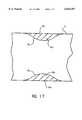
- the aerial image contour 78 with defect deviations 78a, 78bis reproduced along with an overlay of ideal or perfect contours 80a and 80b which would be produced if the mask were not defective.
- An enlarged view of the defective areasis shown in FIG. 17.
- Defective area 82alies between actual contour 78a and ideal contour 80a, while defective area 82b lies between actual contour 78b and ideal contour 80b.
- the controllercalculates the square of the area (82a, 82b) between the ideal and defective aerial image contour.
- the controllerthen cycles through the patch material parameters of transmission, phase and thickness in the lookup table in the system memory 10 to determine which patch would be optimal to adjust the defective area and repair the mask.
- the controllermay also utilize look-up table information to determine whether mask material removal would correct the defect.
- a wide range of metricsmay be used for this and possibly more than one series of calculation may be done simultaneously.
- the softwaredetermines ranges of the optimal patch size, geometry and material parameters of transmission and phase appropriate to the mask repair tool to match the aerial image required. Additionally, the software defines the repaired feature edges and may include optical proximity correction features, as described above, if required.
- the controllerdetermines whether the modeled performance of the repaired defective mask is acceptable. The controller does so by comparing the modeled performance intensity for each point of the aerial image to predetermined tolerances established for each such point in order to process the wafer within established limits. If the calculated performance of the repaired mask is acceptable (box 56), the controller 12 downloads the material deposition process parameters associated with the calculated patches and instructs the mask repair tool 14 to apply the calculated patches to the mask using such deposition parameters. These deposition parameters establish gas flow rates, gas fixtures, time of deposition and other typical process parameters to deposit the patches in the defect area.
- the controllercontinues to iterate through the variable parameters, adjusts the defective mask repair parameters such as transmission percentage, phase shift, thickness and the like and returns to box 50 to redefine the locus of points for the defective mask.
- the processis also performed through various focus values to ensure consistent aerial image integrity through the focus range required to manufacture the desired wafer. The process then continues until the variable parameters achieve a minimum in the square of the area between the It contours of the ideal and simulated repaired mask. Once the modeled performance is within acceptable tolerances, the repair is made by the mask repair tool.
- the present inventionalso contemplates the steps of analyzing the aerial image of the repair patch or material removal and determining whether the patch or removed material sufficiently corrects the defect within predetermined tolerances.
- the present inventionmay be used to add or remove either opaque or transparent attenuating film material to repair defects in the mask. This method allows for optimization of each repair that is made. Each repair that is made is unique and each attenuating film patch or ablation will be optimized to the defect under repair.
Landscapes
- Physics & Mathematics (AREA)
- General Physics & Mathematics (AREA)
- Preparing Plates And Mask In Photomechanical Process (AREA)
- Exposure And Positioning Against Photoresist Photosensitive Materials (AREA)
Abstract
Description
Claims (23)
Priority Applications (2)
| Application Number | Priority Date | Filing Date | Title |
|---|---|---|---|
| US08/876,931US6016357A (en) | 1997-06-16 | 1997-06-16 | Feedback method to repair phase shift masks |
| KR1019980021243AKR100276847B1 (en) | 1997-06-16 | 1998-06-09 | Feedback method and apparatus to repair phase shift masks |
Applications Claiming Priority (1)
| Application Number | Priority Date | Filing Date | Title |
|---|---|---|---|
| US08/876,931US6016357A (en) | 1997-06-16 | 1997-06-16 | Feedback method to repair phase shift masks |
Publications (1)
| Publication Number | Publication Date |
|---|---|
| US6016357Atrue US6016357A (en) | 2000-01-18 |
Family
ID=25368871
Family Applications (1)
| Application Number | Title | Priority Date | Filing Date |
|---|---|---|---|
| US08/876,931Expired - LifetimeUS6016357A (en) | 1997-06-16 | 1997-06-16 | Feedback method to repair phase shift masks |
Country Status (2)
| Country | Link |
|---|---|
| US (1) | US6016357A (en) |
| KR (1) | KR100276847B1 (en) |
Cited By (84)
| Publication number | Priority date | Publication date | Assignee | Title |
|---|---|---|---|---|
| US6175953B1 (en)* | 1998-03-03 | 2001-01-16 | Lsi Logic Corporation | Method and apparatus for general systematic application of proximity correction |
| US20010019625A1 (en)* | 1999-10-13 | 2001-09-06 | Boaz Kenan | Method and apparatus for reticle inspection using aerial imaging |
| US20020035461A1 (en)* | 1997-09-17 | 2002-03-21 | Numerical Technologies, Inc. | Visual analysis and verification system using advanced tools |
| US6373976B1 (en)* | 1997-05-16 | 2002-04-16 | Micron Technology, Inc. | Method and apparatus to accurately correlate defect coordinates between photomask inspection and repair systems |
| US6406818B1 (en)* | 1999-03-31 | 2002-06-18 | Photronics, Inc. | Method of manufacturing photomasks by plasma etching with resist stripped |
| US20020164064A1 (en)* | 2001-03-20 | 2002-11-07 | Numerical Technologies, Inc. | System and method of providing mask quality control |
| US6513151B1 (en)* | 2000-09-14 | 2003-01-28 | Advanced Micro Devices, Inc. | Full flow focus exposure matrix analysis and electrical testing for new product mask evaluation |
| US6560766B2 (en) | 2001-07-26 | 2003-05-06 | Numerical Technologies, Inc. | Method and apparatus for analyzing a layout using an instance-based representation |
| US20030093251A1 (en)* | 2001-11-14 | 2003-05-15 | Numerical Technologies, Inc. | Simulation using design geometry information |
| US6578188B1 (en) | 1997-09-17 | 2003-06-10 | Numerical Technologies, Inc. | Method and apparatus for a network-based mask defect printability analysis system |
| US6593040B2 (en)* | 2000-02-28 | 2003-07-15 | Metron Technology | Method and apparatus for repairing a photomask |
| US20030162105A1 (en)* | 2002-02-28 | 2003-08-28 | Kabushiki Kaisha Toshiba | Method of manufacturing a photomask and method of manufacturing a semiconductor device using the photomask |
| US6615400B1 (en)* | 2001-02-01 | 2003-09-02 | Advanced Micro Devices, Inc. | Optimizing dense via arrays of shrunk integrated circuit designs |
| US20030189863A1 (en)* | 2001-06-14 | 2003-10-09 | Mentor Graphics Corporation | Short edge management in rule based OPC |
| US20030208728A1 (en)* | 2002-05-01 | 2003-11-06 | Numerical Technologies, Inc. | Method and system for simulating resist and etch edges |
| US6649310B2 (en)* | 2000-08-30 | 2003-11-18 | Kabushiki Kaisha Toshiba | Method of manufacturing photomask |
| US20030219154A1 (en)* | 2002-05-22 | 2003-11-27 | Medvedeva Marina M. | Quality measurement of an aerial image |
| US6658640B2 (en) | 2001-12-26 | 2003-12-02 | Numerical Technologies, Inc. | Simulation-based feed forward process control |
| US6660436B1 (en) | 2001-09-17 | 2003-12-09 | Taiwan Semiconductor Manufacturing Company | OPC-like repair method for attenuated phase shift masks |
| US6670082B2 (en) | 2001-10-09 | 2003-12-30 | Numerical Technologies, Inc. | System and method for correcting 3D effects in an alternating phase-shifting mask |
| US20040005089A1 (en)* | 2002-01-31 | 2004-01-08 | Mentor Graphics Corporation | Contrast based resolution enhancing technology |
| WO2004006013A1 (en)* | 2002-07-09 | 2004-01-15 | Carl Zeiss Sms Gmbh | Arrangement for the production of photomasks |
| US20040015808A1 (en)* | 1997-09-17 | 2004-01-22 | Numerical Technologies, Inc. | System and method for providing defect printability analysis of photolithographic masks with job-based automation |
| US20040019872A1 (en)* | 2002-07-24 | 2004-01-29 | George Lippincott | Caching of lithography and etch simulation results |
| US20040049760A1 (en)* | 2002-09-05 | 2004-03-11 | Mario Garza | Wafer process critical dimension, alignment, and registration analysis simulation tool |
| US20040052411A1 (en)* | 2002-09-13 | 2004-03-18 | Numerical Technologies, Inc. | Soft defect printability simulation and analysis for masks |
| US20040058255A1 (en)* | 2002-09-24 | 2004-03-25 | Scott Jessen | Substrate topography compensation at mask design: 3D OPC topography anchored |
| US6721928B2 (en) | 2001-07-26 | 2004-04-13 | Numerical Technologies, Inc. | Verification utilizing instance-based hierarchy management |
| US20040078763A1 (en)* | 2002-10-18 | 2004-04-22 | Lippincott George P. | Short edge smoothing for enhanced scatter bar placement |
| US6745372B2 (en) | 2002-04-05 | 2004-06-01 | Numerical Technologies, Inc. | Method and apparatus for facilitating process-compliant layout optimization |
| US6748578B2 (en)* | 1999-04-30 | 2004-06-08 | Nicolas B. Cobb | Streamlined IC mask layout optical and process correction through correction reuse |
| US6757645B2 (en)* | 1997-09-17 | 2004-06-29 | Numerical Technologies, Inc. | Visual inspection and verification system |
| US20040133871A1 (en)* | 2003-01-02 | 2004-07-08 | Mentor Graphics Corporation. | Matrix optical process correction |
| US20040151991A1 (en)* | 2002-09-18 | 2004-08-05 | Stewart Diane K. | Photolithography mask repair |
| US20040216065A1 (en)* | 2000-07-10 | 2004-10-28 | Cobb Nicolas Bailey | Convergence technique for model-based optical and process correction |
| US20040221254A1 (en)* | 1999-04-30 | 2004-11-04 | Mentor Graphics Corporation | Mixed mode optical proximity correction |
| US20050044513A1 (en)* | 2002-01-31 | 2005-02-24 | Robles Juan Andres Torres | Contrast based resolution enhancement for photolithographic processing |
| US6873720B2 (en) | 2001-03-20 | 2005-03-29 | Synopsys, Inc. | System and method of providing mask defect printability analysis |
| US20050097501A1 (en)* | 2003-10-31 | 2005-05-05 | Mentor Graphics Corporation | Site control for OPC |
| US20050153214A1 (en)* | 2004-01-12 | 2005-07-14 | Taiwan Semiconductor Manufacturing Co. | Single trench repair method with etched quartz for attenuated phase shifting mask |
| US20050185173A1 (en)* | 2004-02-20 | 2005-08-25 | The Regents Of The University Of California | Method for characterizing mask defects using image reconstruction from X-ray diffraction patterns |
| US20050198598A1 (en)* | 2004-02-24 | 2005-09-08 | Konstantinos Adam | OPC simulation model using SOCS decomposition of edge fragments |
| US20050216878A1 (en)* | 2004-02-25 | 2005-09-29 | James Word | Long range corrections in integrated circuit layout designs |
| US20050251771A1 (en)* | 2004-05-07 | 2005-11-10 | Mentor Graphics Corporation | Integrated circuit layout design methodology with process variation bands |
| US20050273733A1 (en)* | 2004-06-02 | 2005-12-08 | Lippincott George P | OPC conflict identification and edge priority system |
| US20050278686A1 (en)* | 2004-02-25 | 2005-12-15 | James Word | Fragmentation point and simulation site adjustment for resolution enhancement techniques |
| US20050283747A1 (en)* | 2004-02-24 | 2005-12-22 | Konstantinos Adam | OPC simulation model using SOCS decomposition of edge fragments |
| US20060005154A1 (en)* | 2000-06-13 | 2006-01-05 | Mentor Graphics Corporation | Integrated OPC verification tool |
| US6999611B1 (en)* | 1999-02-13 | 2006-02-14 | Kla-Tencor Corporation | Reticle defect detection using simulation |
| US7014955B2 (en) | 2001-08-28 | 2006-03-21 | Synopsys, Inc. | System and method for indentifying dummy features on a mask layer |
| US7072502B2 (en) | 2001-06-07 | 2006-07-04 | Applied Materials, Inc. | Alternating phase-shift mask inspection method and apparatus |
| US20060151791A1 (en)* | 1999-07-06 | 2006-07-13 | Semiconductor Energy Laboratory Co., Ltd. | Semiconductor device and method of fabricating the same |
| DE102005004070B3 (en)* | 2005-01-28 | 2006-08-03 | Infineon Technologies Ag | Lithographic mask`s defective material removing method for highly integrated circuit, involves applying absorbing material in outer region after removal of defective material to form transmitting region with desired phase difference on mask |
| US20060188796A1 (en)* | 2005-02-24 | 2006-08-24 | James Word | Performing OPC on structures with virtual edges |
| US20060200790A1 (en)* | 2005-03-02 | 2006-09-07 | Shang Shumay D | Model-based SRAF insertion |
| US20060199084A1 (en)* | 2005-03-02 | 2006-09-07 | Mentor Graphics Corporation | Chromeless phase shifting mask for integrated circuits |
| US20060204862A1 (en)* | 2005-03-14 | 2006-09-14 | Samsung Electronics Co., Ltd. | Methods, systems and computer program products for correcting photomask using aerial images and boundary regions |
| US20060209309A1 (en)* | 2005-03-18 | 2006-09-21 | Illumina, Inc. | Systems for and methods of facilitating focusing an optical scanner |
| US7112390B2 (en) | 2002-07-15 | 2006-09-26 | Samsung Electronics Co., Ltd. | Method of manufacturing chromeless phase shift mask |
| US20060242619A1 (en)* | 1997-09-17 | 2006-10-26 | Synopsys, Inc. | System And Method For Providing Defect Printability Analysis Of Photolithographic Masks With Job-Based Automation |
| US20060288325A1 (en)* | 2005-06-15 | 2006-12-21 | Atsushi Miyamoto | Method and apparatus for measuring dimension of a pattern formed on a semiconductor wafer |
| US20070074143A1 (en)* | 2005-09-27 | 2007-03-29 | Nicolas Bailey Cobb | Dense OPC |
| US20070198967A1 (en)* | 2006-02-17 | 2007-08-23 | Zhuoxiang Ren | Computation of electrical properties of an ic layout |
| US20080015818A1 (en)* | 2004-03-03 | 2008-01-17 | Taiwan Semiconductor Manufacturing Co., Ltd. | Method and system for mask fabrication process control |
| US20080050010A1 (en)* | 2006-07-26 | 2008-02-28 | Elpida Memory, Inc. | Apparatus for correcting defects in a reticle pattern and correcting method for the same |
| US20080141195A1 (en)* | 2006-11-09 | 2008-06-12 | Juan Andres Torres Robles | Analysis optimizer |
| US20080148217A1 (en)* | 2006-12-13 | 2008-06-19 | Jea-Woo Park | Selective shielding for multiple exposure masks |
| US20080166639A1 (en)* | 2007-01-08 | 2008-07-10 | Jea-Woo Park | Data preparation for multiple mask printing |
| US20080195996A1 (en)* | 2007-02-09 | 2008-08-14 | Juan Andres Torres Robles | Pre-bias optical proximity correction |
| US20080193859A1 (en)* | 2007-02-09 | 2008-08-14 | Ayman Yehia Hamouda | Dual metric opc |
| US20080256500A1 (en)* | 2000-06-13 | 2008-10-16 | Cobb Nicolas B | Integrated opc verification tool |
| US20090060317A1 (en)* | 2007-08-31 | 2009-03-05 | William Volk | Mask defect repair through wafer plane modeling |
| US7506285B2 (en) | 2006-02-17 | 2009-03-17 | Mohamed Al-Imam | Multi-dimensional analysis for predicting RET model accuracy |
| US20090100389A1 (en)* | 2007-10-11 | 2009-04-16 | Ir Kusnadi | Shape-based photolithographic model calibration |
| DE102007054994A1 (en)* | 2007-11-17 | 2009-05-20 | Carl Zeiss Sms Gmbh | Method of repairing phase shift masks |
| US20090262317A1 (en)* | 2008-04-18 | 2009-10-22 | International Business Machines Corporation | Test method for determining reticle transmission stability |
| US20100254591A1 (en)* | 2009-04-07 | 2010-10-07 | Carl Zeiss Sms Gmbh | Verification method for repairs on photolithography masks |
| EP1269264B1 (en)* | 2000-02-29 | 2011-03-23 | GlobalFoundries, Inc. | Method of analyzing a wafer manufacturing process |
| WO2011161243A1 (en) | 2010-06-23 | 2011-12-29 | Carl Zeiss Sms Gmbh | Method and apparatus for analyzing and / or repairing of an euv mask defect |
| US8124300B1 (en)* | 2004-11-30 | 2012-02-28 | Globalfoundries Inc. | Method of lithographic mask correction using localized transmission adjustment |
| US8713483B2 (en) | 2007-06-05 | 2014-04-29 | Mentor Graphics Corporation | IC layout parsing for multiple masks |
| US20140212021A1 (en)* | 2013-01-31 | 2014-07-31 | Applied Materials Israel Ltd. | System, a method and a computer program product for patch-based defect detection |
| US10216890B2 (en) | 2004-04-21 | 2019-02-26 | Iym Technologies Llc | Integrated circuits having in-situ constraints |
| JP2021189200A (en)* | 2020-05-25 | 2021-12-13 | 株式会社エスケーエレクトロニクス | How to fix a photomask |
Families Citing this family (1)
| Publication number | Priority date | Publication date | Assignee | Title |
|---|---|---|---|---|
| KR100588910B1 (en)* | 2004-12-22 | 2006-06-09 | 동부일렉트로닉스 주식회사 | Manufacturing method of halftone phase inversion mask of semiconductor device |
Citations (15)
| Publication number | Priority date | Publication date | Assignee | Title |
|---|---|---|---|---|
| US4906326A (en)* | 1988-03-25 | 1990-03-06 | Canon Kabushiki Kaisha | Mask repair system |
| US5085957A (en)* | 1990-04-18 | 1992-02-04 | Mitsubishi Denki Kabushiki Kaisha | Method of repairing a mask |
| JPH055979A (en)* | 1990-10-05 | 1993-01-14 | Sharp Corp | Light exposure mask, manufacturing method thereof, and repair method thereof |
| US5246804A (en)* | 1988-11-08 | 1993-09-21 | Kyodo Printing Co., Ltd. | Method of retouching pattern |
| US5273849A (en)* | 1987-11-09 | 1993-12-28 | At&T Bell Laboratories | Mask repair |
| US5318869A (en)* | 1989-06-06 | 1994-06-07 | Dai Nippon Insatsu Kabushiki Kaisha | Method and apparatus for repairing defects in emulsion masks and the like |
| JPH06282064A (en)* | 1993-03-29 | 1994-10-07 | Toppan Printing Co Ltd | Production of phase shift mask with auxiliary pattern |
| EP0627664A1 (en)* | 1993-06-04 | 1994-12-07 | International Business Machines Corporation | Method for the repair of phase shifting masks |
| US5382484A (en)* | 1992-08-21 | 1995-01-17 | Mitsubishi Denki Kabushiki Kaisha | Method of correcting defects in the pattern of phase shift mask |
| US5443931A (en)* | 1992-03-31 | 1995-08-22 | Matsushita Electronics Corporation | Photo mask and repair method of the same |
| US5468337A (en)* | 1992-06-02 | 1995-11-21 | Mitsubishi Denki Kabushiki Kaisha | Method of mending a defect in a phase shift pattern |
| US5795688A (en)* | 1996-08-14 | 1998-08-18 | Micron Technology, Inc. | Process for detecting defects in photomasks through aerial image comparisons |
| US5795685A (en)* | 1997-01-14 | 1998-08-18 | International Business Machines Corporation | Simple repair method for phase shifting masks |
| US5801954A (en)* | 1996-04-24 | 1998-09-01 | Micron Technology, Inc. | Process for designing and checking a mask layout |
| US5849440A (en)* | 1996-07-02 | 1998-12-15 | Motorola, Inc. | Process for producing and inspecting a lithographic reticle and fabricating semiconductor devices using same |
- 1997
- 1997-06-16USUS08/876,931patent/US6016357A/ennot_activeExpired - Lifetime
- 1998
- 1998-06-09KRKR1019980021243Apatent/KR100276847B1/ennot_activeExpired - Fee Related
Patent Citations (15)
| Publication number | Priority date | Publication date | Assignee | Title |
|---|---|---|---|---|
| US5273849A (en)* | 1987-11-09 | 1993-12-28 | At&T Bell Laboratories | Mask repair |
| US4906326A (en)* | 1988-03-25 | 1990-03-06 | Canon Kabushiki Kaisha | Mask repair system |
| US5246804A (en)* | 1988-11-08 | 1993-09-21 | Kyodo Printing Co., Ltd. | Method of retouching pattern |
| US5318869A (en)* | 1989-06-06 | 1994-06-07 | Dai Nippon Insatsu Kabushiki Kaisha | Method and apparatus for repairing defects in emulsion masks and the like |
| US5085957A (en)* | 1990-04-18 | 1992-02-04 | Mitsubishi Denki Kabushiki Kaisha | Method of repairing a mask |
| JPH055979A (en)* | 1990-10-05 | 1993-01-14 | Sharp Corp | Light exposure mask, manufacturing method thereof, and repair method thereof |
| US5443931A (en)* | 1992-03-31 | 1995-08-22 | Matsushita Electronics Corporation | Photo mask and repair method of the same |
| US5468337A (en)* | 1992-06-02 | 1995-11-21 | Mitsubishi Denki Kabushiki Kaisha | Method of mending a defect in a phase shift pattern |
| US5382484A (en)* | 1992-08-21 | 1995-01-17 | Mitsubishi Denki Kabushiki Kaisha | Method of correcting defects in the pattern of phase shift mask |
| JPH06282064A (en)* | 1993-03-29 | 1994-10-07 | Toppan Printing Co Ltd | Production of phase shift mask with auxiliary pattern |
| EP0627664A1 (en)* | 1993-06-04 | 1994-12-07 | International Business Machines Corporation | Method for the repair of phase shifting masks |
| US5801954A (en)* | 1996-04-24 | 1998-09-01 | Micron Technology, Inc. | Process for designing and checking a mask layout |
| US5849440A (en)* | 1996-07-02 | 1998-12-15 | Motorola, Inc. | Process for producing and inspecting a lithographic reticle and fabricating semiconductor devices using same |
| US5795688A (en)* | 1996-08-14 | 1998-08-18 | Micron Technology, Inc. | Process for detecting defects in photomasks through aerial image comparisons |
| US5795685A (en)* | 1997-01-14 | 1998-08-18 | International Business Machines Corporation | Simple repair method for phase shifting masks |
Non-Patent Citations (8)
| Title |
|---|
| Elimination of Mask Substrate Defects, IBM Technical Disclosure Bulletin, vol. 26, No. 7B, Dec. 1983 R. L. West.* |
| Elimination of Mask Substrate Defects, IBM Technical Disclosure Bulletin, vol. 26, No. 7B, Dec. 1983--R. L. West. |
| Method for Repairing a Short Defect After The Forming Process of A Passivation Layer, IBM Technical Disclosure Bulletin, vol. 39, No. 02, Feb. 1996.* |
| Method For Repairing Hard Mask, by N. Chand, Sep. 1972, TDBS Sep. 1972, p. 1345.* |
| Method of Producing Defect Free Transmission Masks, IBM Technical Disclosure Bulletin, vol. 27, No. 8, Jan. 1985 U. Behringer, W. Kulcke, P. Nehmiz and W. Zapka.* |
| Method of Producing Defect-Free Transmission Masks, IBM Technical Disclosure Bulletin, vol. 27, No. 8, Jan. 1985--U. Behringer, W. Kulcke, P. Nehmiz and W. Zapka. |
| Repair System for Phase Shift Masks, IBM Technical Disclosure Bulletin, vol. 36, No. 05, May 1993.* |
| Repair Technique for Eleiminating Discontinuities In Patterned Metallurgy TDBS, by R. Hammer, Sep. 1977, p. 1596.* |
Cited By (201)
| Publication number | Priority date | Publication date | Assignee | Title |
|---|---|---|---|---|
| US6373976B1 (en)* | 1997-05-16 | 2002-04-16 | Micron Technology, Inc. | Method and apparatus to accurately correlate defect coordinates between photomask inspection and repair systems |
| US20030126581A1 (en)* | 1997-09-17 | 2003-07-03 | Numerical Technologies, Inc. | User interface for a network-based mask defect printability analysis system |
| US7003755B2 (en) | 1997-09-17 | 2006-02-21 | Synopsys Inc. | User interface for a networked-based mask defect printability analysis system |
| US20020035461A1 (en)* | 1997-09-17 | 2002-03-21 | Numerical Technologies, Inc. | Visual analysis and verification system using advanced tools |
| US7093229B2 (en) | 1997-09-17 | 2006-08-15 | Synopsys, Inc. | System and method for providing defect printability analysis of photolithographic masks with job-based automation |
| US6757645B2 (en)* | 1997-09-17 | 2004-06-29 | Numerical Technologies, Inc. | Visual inspection and verification system |
| US20040015808A1 (en)* | 1997-09-17 | 2004-01-22 | Numerical Technologies, Inc. | System and method for providing defect printability analysis of photolithographic masks with job-based automation |
| US20060242619A1 (en)* | 1997-09-17 | 2006-10-26 | Synopsys, Inc. | System And Method For Providing Defect Printability Analysis Of Photolithographic Masks With Job-Based Automation |
| US7107571B2 (en) | 1997-09-17 | 2006-09-12 | Synopsys, Inc. | Visual analysis and verification system using advanced tools |
| US7617474B2 (en) | 1997-09-17 | 2009-11-10 | Synopsys, Inc. | System and method for providing defect printability analysis of photolithographic masks with job-based automation |
| US6578188B1 (en) | 1997-09-17 | 2003-06-10 | Numerical Technologies, Inc. | Method and apparatus for a network-based mask defect printability analysis system |
| US6175953B1 (en)* | 1998-03-03 | 2001-01-16 | Lsi Logic Corporation | Method and apparatus for general systematic application of proximity correction |
| US6999611B1 (en)* | 1999-02-13 | 2006-02-14 | Kla-Tencor Corporation | Reticle defect detection using simulation |
| US6406818B1 (en)* | 1999-03-31 | 2002-06-18 | Photronics, Inc. | Method of manufacturing photomasks by plasma etching with resist stripped |
| US6562549B2 (en) | 1999-03-31 | 2003-05-13 | Photronics, Inc. | Method of manufacturing photomasks by plasma etching with resist stripped |
| US20040221254A1 (en)* | 1999-04-30 | 2004-11-04 | Mentor Graphics Corporation | Mixed mode optical proximity correction |
| US20050160388A1 (en)* | 1999-04-30 | 2005-07-21 | Mentor Graphics Corporation | Streamlined IC mask layout optical and process correction through correction reuse |
| US6748578B2 (en)* | 1999-04-30 | 2004-06-08 | Nicolas B. Cobb | Streamlined IC mask layout optical and process correction through correction reuse |
| US7155699B2 (en) | 1999-04-30 | 2006-12-26 | Cobb Nicolas B | Streamlined IC mask layout optical and process correction through correction reuse |
| US20060151791A1 (en)* | 1999-07-06 | 2006-07-13 | Semiconductor Energy Laboratory Co., Ltd. | Semiconductor device and method of fabricating the same |
| US20010019625A1 (en)* | 1999-10-13 | 2001-09-06 | Boaz Kenan | Method and apparatus for reticle inspection using aerial imaging |
| US7133548B2 (en) | 1999-10-13 | 2006-11-07 | Applied Materials, Inc. | Method and apparatus for reticle inspection using aerial imaging |
| US6593040B2 (en)* | 2000-02-28 | 2003-07-15 | Metron Technology | Method and apparatus for repairing a photomask |
| US20030207184A1 (en)* | 2000-02-28 | 2003-11-06 | Eryn Smith | Method and apparatus for repairing an alternating phase shift mask |
| EP1269264B1 (en)* | 2000-02-29 | 2011-03-23 | GlobalFoundries, Inc. | Method of analyzing a wafer manufacturing process |
| US7945871B2 (en) | 2000-06-13 | 2011-05-17 | Cobb Nicolas B | Integrated OPC verification tool |
| US7412676B2 (en) | 2000-06-13 | 2008-08-12 | Nicolas B Cobb | Integrated OPC verification tool |
| US20080256500A1 (en)* | 2000-06-13 | 2008-10-16 | Cobb Nicolas B | Integrated opc verification tool |
| US20060005154A1 (en)* | 2000-06-13 | 2006-01-05 | Mentor Graphics Corporation | Integrated OPC verification tool |
| US7028284B2 (en) | 2000-07-10 | 2006-04-11 | Nicolas Bailey Cobb | Convergence technique for model-based optical and process correction |
| US20040216065A1 (en)* | 2000-07-10 | 2004-10-28 | Cobb Nicolas Bailey | Convergence technique for model-based optical and process correction |
| US7367009B2 (en) | 2000-07-10 | 2008-04-29 | Mentor Graphics Corporation | Convergence technique for model-based optical and process correction |
| US6649310B2 (en)* | 2000-08-30 | 2003-11-18 | Kabushiki Kaisha Toshiba | Method of manufacturing photomask |
| US6513151B1 (en)* | 2000-09-14 | 2003-01-28 | Advanced Micro Devices, Inc. | Full flow focus exposure matrix analysis and electrical testing for new product mask evaluation |
| US6615400B1 (en)* | 2001-02-01 | 2003-09-02 | Advanced Micro Devices, Inc. | Optimizing dense via arrays of shrunk integrated circuit designs |
| US20020164064A1 (en)* | 2001-03-20 | 2002-11-07 | Numerical Technologies, Inc. | System and method of providing mask quality control |
| US6873720B2 (en) | 2001-03-20 | 2005-03-29 | Synopsys, Inc. | System and method of providing mask defect printability analysis |
| US20080260235A1 (en)* | 2001-03-20 | 2008-10-23 | Synopsys, Inc. | System And Method Of Providing Mask Defect Printability Analysis |
| US7254251B2 (en) | 2001-03-20 | 2007-08-07 | Synopsys, Inc. | System and method of providing mask defect printability analysis |
| US7403649B2 (en) | 2001-03-20 | 2008-07-22 | Synopsys, Inc. | System and method of providing mask defect printability analysis |
| US7565001B2 (en) | 2001-03-20 | 2009-07-21 | Synopsys, Inc. | System and method of providing mask defect printability analysis |
| US6925202B2 (en)* | 2001-03-20 | 2005-08-02 | Synopsys, Inc. | System and method of providing mask quality control |
| US20050190957A1 (en)* | 2001-03-20 | 2005-09-01 | Synopsys, Inc. | System and method of providing mask defect printability analysis |
| US7835565B2 (en) | 2001-03-20 | 2010-11-16 | Synopsys, Inc. | System and method of providing mask defect printability analysis |
| US20090245621A1 (en)* | 2001-03-20 | 2009-10-01 | Synopsys, Inc, | System And Method Of Providing Mask Defect Printability Analysis |
| US7072502B2 (en) | 2001-06-07 | 2006-07-04 | Applied Materials, Inc. | Alternating phase-shift mask inspection method and apparatus |
| US7181721B2 (en) | 2001-06-14 | 2007-02-20 | Lippincott George P | Short edge management in rule based OPC |
| US20040230930A1 (en)* | 2001-06-14 | 2004-11-18 | Mentor Graphics Corporation | Short edge management in rule based OPC |
| US20030189863A1 (en)* | 2001-06-14 | 2003-10-09 | Mentor Graphics Corporation | Short edge management in rule based OPC |
| US6817003B2 (en) | 2001-06-14 | 2004-11-09 | Lippincott George P | Short edge management in rule based OPC |
| US6560766B2 (en) | 2001-07-26 | 2003-05-06 | Numerical Technologies, Inc. | Method and apparatus for analyzing a layout using an instance-based representation |
| US6721928B2 (en) | 2001-07-26 | 2004-04-13 | Numerical Technologies, Inc. | Verification utilizing instance-based hierarchy management |
| US7014955B2 (en) | 2001-08-28 | 2006-03-21 | Synopsys, Inc. | System and method for indentifying dummy features on a mask layer |
| US6660436B1 (en) | 2001-09-17 | 2003-12-09 | Taiwan Semiconductor Manufacturing Company | OPC-like repair method for attenuated phase shift masks |
| US20040076895A1 (en)* | 2001-10-09 | 2004-04-22 | Numerical Technologies, Inc. | System and method for correcting 3D effects in an alternating phase-shifting mask |
| US6670082B2 (en) | 2001-10-09 | 2003-12-30 | Numerical Technologies, Inc. | System and method for correcting 3D effects in an alternating phase-shifting mask |
| US6830854B2 (en) | 2001-10-09 | 2004-12-14 | Numerical Technologies, Inc. | System and method for correcting 3D effects in an alternating phase-shifting mask |
| US20030093251A1 (en)* | 2001-11-14 | 2003-05-15 | Numerical Technologies, Inc. | Simulation using design geometry information |
| US6976240B2 (en) | 2001-11-14 | 2005-12-13 | Synopsys Inc. | Simulation using design geometry information |
| US6658640B2 (en) | 2001-12-26 | 2003-12-02 | Numerical Technologies, Inc. | Simulation-based feed forward process control |
| US7013439B2 (en) | 2002-01-31 | 2006-03-14 | Juan Andres Torres Robles | Contrast based resolution enhancing technology |
| US8108806B2 (en) | 2002-01-31 | 2012-01-31 | Mentor Graphics Corporation | Contrast-based resolution enhancement for photolithographic processing |
| US20090271759A1 (en)* | 2002-01-31 | 2009-10-29 | Juan Andres Torres Robles | Contrast-based resolution enhancement for photolithographic processing |
| US7562336B2 (en) | 2002-01-31 | 2009-07-14 | Juan Andres Torres Robles | Contrast based resolution enhancement for photolithographic processing |
| US20070124708A1 (en)* | 2002-01-31 | 2007-05-31 | Torres Robles Juan A | Contrast based resolution enhancement for photolithographic processing |
| US20050044513A1 (en)* | 2002-01-31 | 2005-02-24 | Robles Juan Andres Torres | Contrast based resolution enhancement for photolithographic processing |
| US7293249B2 (en) | 2002-01-31 | 2007-11-06 | Juan Andres Torres Robles | Contrast based resolution enhancement for photolithographic processing |
| US20040005089A1 (en)* | 2002-01-31 | 2004-01-08 | Mentor Graphics Corporation | Contrast based resolution enhancing technology |
| US20030162105A1 (en)* | 2002-02-28 | 2003-08-28 | Kabushiki Kaisha Toshiba | Method of manufacturing a photomask and method of manufacturing a semiconductor device using the photomask |
| US7008731B2 (en) | 2002-02-28 | 2006-03-07 | Kabushiki Kaisha Toshiba | Method of manufacturing a photomask and method of manufacturing a semiconductor device using the photomask |
| US6745372B2 (en) | 2002-04-05 | 2004-06-01 | Numerical Technologies, Inc. | Method and apparatus for facilitating process-compliant layout optimization |
| US20030208728A1 (en)* | 2002-05-01 | 2003-11-06 | Numerical Technologies, Inc. | Method and system for simulating resist and etch edges |
| US6954911B2 (en) | 2002-05-01 | 2005-10-11 | Synopsys, Inc. | Method and system for simulating resist and etch edges |
| US7035446B2 (en)* | 2002-05-22 | 2006-04-25 | Lsi Logic Corporation | Quality measurement of an aerial image |
| US20030219154A1 (en)* | 2002-05-22 | 2003-11-27 | Medvedeva Marina M. | Quality measurement of an aerial image |
| WO2004006013A1 (en)* | 2002-07-09 | 2004-01-15 | Carl Zeiss Sms Gmbh | Arrangement for the production of photomasks |
| US7112390B2 (en) | 2002-07-15 | 2006-09-26 | Samsung Electronics Co., Ltd. | Method of manufacturing chromeless phase shift mask |
| US20040019872A1 (en)* | 2002-07-24 | 2004-01-29 | George Lippincott | Caching of lithography and etch simulation results |
| US6973633B2 (en) | 2002-07-24 | 2005-12-06 | George Lippincott | Caching of lithography and etch simulation results |
| US20040049760A1 (en)* | 2002-09-05 | 2004-03-11 | Mario Garza | Wafer process critical dimension, alignment, and registration analysis simulation tool |
| US6782525B2 (en)* | 2002-09-05 | 2004-08-24 | Lsi Logic Corporation | Wafer process critical dimension, alignment, and registration analysis simulation tool |
| US20040052411A1 (en)* | 2002-09-13 | 2004-03-18 | Numerical Technologies, Inc. | Soft defect printability simulation and analysis for masks |
| US7043071B2 (en)* | 2002-09-13 | 2006-05-09 | Synopsys, Inc. | Soft defect printability simulation and analysis for masks |
| US7662524B2 (en) | 2002-09-18 | 2010-02-16 | Fei Company | Photolithography mask repair |
| EP1540665A4 (en)* | 2002-09-18 | 2008-02-13 | Fei Co | Photolithography mask repair |
| US20040151991A1 (en)* | 2002-09-18 | 2004-08-05 | Stewart Diane K. | Photolithography mask repair |
| US7504182B2 (en)* | 2002-09-18 | 2009-03-17 | Fei Company | Photolithography mask repair |
| US20090111036A1 (en)* | 2002-09-18 | 2009-04-30 | Fei Company | Photolithography mask repair |
| US6893800B2 (en) | 2002-09-24 | 2005-05-17 | Agere Systems, Inc. | Substrate topography compensation at mask design: 3D OPC topography anchored |
| US20040058255A1 (en)* | 2002-09-24 | 2004-03-25 | Scott Jessen | Substrate topography compensation at mask design: 3D OPC topography anchored |
| US7281234B2 (en) | 2002-10-18 | 2007-10-09 | George P Lippincott | Short edge smoothing for enhanced scatter bar placement |
| US20040078763A1 (en)* | 2002-10-18 | 2004-04-22 | Lippincott George P. | Short edge smoothing for enhanced scatter bar placement |
| US20050208396A1 (en)* | 2002-10-18 | 2005-09-22 | Mentor Graphics Corporation | Short edge smoothing for enhanced scatter bar placement |
| US6857109B2 (en) | 2002-10-18 | 2005-02-15 | George P. Lippincott | Short edge smoothing for enhanced scatter bar placement |
| US7237221B2 (en) | 2003-01-02 | 2007-06-26 | Yuri Granik | Matrix optical process correction |
| US6928634B2 (en) | 2003-01-02 | 2005-08-09 | Yuri Granik | Matrix optical process correction |
| US20050278685A1 (en)* | 2003-01-02 | 2005-12-15 | Mentor Graphics Corporation | Matrix optical process correction |
| US20040133871A1 (en)* | 2003-01-02 | 2004-07-08 | Mentor Graphics Corporation. | Matrix optical process correction |
| US20050097501A1 (en)* | 2003-10-31 | 2005-05-05 | Mentor Graphics Corporation | Site control for OPC |
| US7073162B2 (en) | 2003-10-31 | 2006-07-04 | Mentor Graphics Corporation | Site control for OPC |
| US20050153214A1 (en)* | 2004-01-12 | 2005-07-14 | Taiwan Semiconductor Manufacturing Co. | Single trench repair method with etched quartz for attenuated phase shifting mask |
| US7157191B2 (en) | 2004-01-12 | 2007-01-02 | Taiwan Semiconductor Manufacturing Co., Ltd. | Single trench repair method with etched quartz for attenuated phase shifting mask |
| US20060234141A1 (en)* | 2004-01-12 | 2006-10-19 | Taiwan Semiconductor Manufacturing Co., Ltd. | Single trench repair method with etched quartz for attenuated phase shifting mask |
| US7393617B2 (en) | 2004-01-12 | 2008-07-01 | Taiwan Semiconductor Manufacturing Co., Ltd. | Single trench repair method with etched quartz for attenuated phase shifting mask |
| US20050185173A1 (en)* | 2004-02-20 | 2005-08-25 | The Regents Of The University Of California | Method for characterizing mask defects using image reconstruction from X-ray diffraction patterns |
| US7212282B2 (en)* | 2004-02-20 | 2007-05-01 | The Regents Of The University Of California | Method for characterizing mask defects using image reconstruction from X-ray diffraction patterns |
| US7539954B2 (en) | 2004-02-24 | 2009-05-26 | Konstantinos Adam | OPC simulation model using SOCS decomposition of edge fragments |
| US20050198598A1 (en)* | 2004-02-24 | 2005-09-08 | Konstantinos Adam | OPC simulation model using SOCS decomposition of edge fragments |
| US20090217218A1 (en)* | 2004-02-24 | 2009-08-27 | Konstantinos Adam | Opc simulation model using socs decomposition of edge fragments |
| US20050283747A1 (en)* | 2004-02-24 | 2005-12-22 | Konstantinos Adam | OPC simulation model using SOCS decomposition of edge fragments |
| US7536660B2 (en) | 2004-02-24 | 2009-05-19 | Konstantinos Adam | OPC simulation model using SOCS decomposition of edge fragments |
| US7234130B2 (en) | 2004-02-25 | 2007-06-19 | James Word | Long range corrections in integrated circuit layout designs |
| US9361422B2 (en) | 2004-02-25 | 2016-06-07 | Mentor Graphics Corporation | Fragmentation point and simulation site adjustment for resolution enhancement techniques |
| US7861207B2 (en) | 2004-02-25 | 2010-12-28 | Mentor Graphics Corporation | Fragmentation point and simulation site adjustment for resolution enhancement techniques |
| US20050216878A1 (en)* | 2004-02-25 | 2005-09-29 | James Word | Long range corrections in integrated circuit layout designs |
| US20050278686A1 (en)* | 2004-02-25 | 2005-12-15 | James Word | Fragmentation point and simulation site adjustment for resolution enhancement techniques |
| US10354044B2 (en) | 2004-02-25 | 2019-07-16 | Mentor Graphics Corporation | Fragmentation point and simulation site adjustment for resolution enhancement techniques |
| US8566753B2 (en) | 2004-02-25 | 2013-10-22 | Mentor Graphics Corporation | Fragmentation point and simulation site adjustment for resolution enhancement techniques |
| US20110161894A1 (en)* | 2004-02-25 | 2011-06-30 | Mentor Graphics Corporation | Fragmentation point and simulation site adjustment for resolution enhancement techniques |
| US9703922B2 (en) | 2004-02-25 | 2017-07-11 | Mentor Graphics Corporation | Fragmentation point and simulation site adjustment for resolution enhancement techniques |
| US20080015818A1 (en)* | 2004-03-03 | 2008-01-17 | Taiwan Semiconductor Manufacturing Co., Ltd. | Method and system for mask fabrication process control |
| US8082119B2 (en)* | 2004-03-03 | 2011-12-20 | Taiwan Semiconductor Manufacturing Co., Ltd. | Method and system for mask fabrication process control |
| US10216890B2 (en) | 2004-04-21 | 2019-02-26 | Iym Technologies Llc | Integrated circuits having in-situ constraints |
| US10846454B2 (en) | 2004-04-21 | 2020-11-24 | Iym Technologies Llc | Integrated circuits having in-situ constraints |
| US10860773B2 (en) | 2004-04-21 | 2020-12-08 | Iym Technologies Llc | Integrated circuits having in-situ constraints |
| US9361424B2 (en) | 2004-05-07 | 2016-06-07 | Mentor Graphics Corporation | Integrated circuit layout design methodology with process variation bands |
| US20050251771A1 (en)* | 2004-05-07 | 2005-11-10 | Mentor Graphics Corporation | Integrated circuit layout design methodology with process variation bands |
| US8799830B2 (en) | 2004-05-07 | 2014-08-05 | Mentor Graphics Corporation | Integrated circuit layout design methodology with process variation bands |
| US9977856B2 (en) | 2004-05-07 | 2018-05-22 | Mentor Graphics Corporation | Integrated circuit layout design methodology with process variation bands |
| US20050273733A1 (en)* | 2004-06-02 | 2005-12-08 | Lippincott George P | OPC conflict identification and edge priority system |
| US20070118826A1 (en)* | 2004-06-02 | 2007-05-24 | Lippincott George P | Opc conflict identification and edge priority system |
| US8806390B2 (en) | 2004-06-02 | 2014-08-12 | Mentor Graphics Corporation | OPC conflict identification and edge priority system |
| US7240305B2 (en) | 2004-06-02 | 2007-07-03 | Lippincott George P | OPC conflict identification and edge priority system |
| US7865863B2 (en) | 2004-06-02 | 2011-01-04 | Mentor Graphics Corporation | OPC conflict identification and edge priority system |
| US20110167394A1 (en)* | 2004-06-02 | 2011-07-07 | Mentor Graphics Corporation | Opc conflict identification and edge priority system |
| US8124300B1 (en)* | 2004-11-30 | 2012-02-28 | Globalfoundries Inc. | Method of lithographic mask correction using localized transmission adjustment |
| US20070037071A1 (en)* | 2005-01-28 | 2007-02-15 | Qimonda Ag | Method for removing defect material of a lithography mask |
| DE102005004070B3 (en)* | 2005-01-28 | 2006-08-03 | Infineon Technologies Ag | Lithographic mask`s defective material removing method for highly integrated circuit, involves applying absorbing material in outer region after removal of defective material to form transmitting region with desired phase difference on mask |
| US7459248B2 (en) | 2005-02-24 | 2008-12-02 | James Word | Performing OPC on structures with virtual edges |
| US20060188796A1 (en)* | 2005-02-24 | 2006-08-24 | James Word | Performing OPC on structures with virtual edges |
| US7493587B2 (en) | 2005-03-02 | 2009-02-17 | James Word | Chromeless phase shifting mask for integrated circuits using interior region |
| US20060199084A1 (en)* | 2005-03-02 | 2006-09-07 | Mentor Graphics Corporation | Chromeless phase shifting mask for integrated circuits |
| US8037429B2 (en) | 2005-03-02 | 2011-10-11 | Mentor Graphics Corporation | Model-based SRAF insertion |
| US20060200790A1 (en)* | 2005-03-02 | 2006-09-07 | Shang Shumay D | Model-based SRAF insertion |
| US20060204862A1 (en)* | 2005-03-14 | 2006-09-14 | Samsung Electronics Co., Ltd. | Methods, systems and computer program products for correcting photomask using aerial images and boundary regions |
| US7389491B2 (en)* | 2005-03-14 | 2008-06-17 | Samsung Electronics Co., Ltd. | Methods, systems and computer program products for correcting photomask using aerial images and boundary regions |
| US20060209309A1 (en)* | 2005-03-18 | 2006-09-21 | Illumina, Inc. | Systems for and methods of facilitating focusing an optical scanner |
| US8867029B2 (en) | 2005-03-18 | 2014-10-21 | Illumina, Inc. | Systems for and methods of facilitating focusing an optical scanner |
| US9201230B2 (en) | 2005-03-18 | 2015-12-01 | Illumina, Inc. | Systems for and methods of facilitating focusing an optical scanner |
| US20100259763A1 (en)* | 2005-03-18 | 2010-10-14 | Illumina Inc. | Systems for and methods of facilitating focusing an optical scanner |
| WO2006101686A3 (en)* | 2005-03-18 | 2011-06-03 | Illumina, Inc. | Systems for and methods of facilitating focusing an optical scanner |
| US7768638B2 (en)* | 2005-03-18 | 2010-08-03 | Illumina, Inc. | Systems for and methods of facilitating focusing an optical scanner |
| US20060288325A1 (en)* | 2005-06-15 | 2006-12-21 | Atsushi Miyamoto | Method and apparatus for measuring dimension of a pattern formed on a semiconductor wafer |
| USRE45224E1 (en)* | 2005-06-15 | 2014-10-28 | Hitachi High-Technologies Corporation | Method and apparatus for creating imaging recipe |
| USRE45204E1 (en)* | 2005-06-15 | 2014-10-21 | Hitachi High-Technologies Corporation | Method and apparatus for creating imaging recipe |
| US7559047B2 (en)* | 2005-06-15 | 2009-07-07 | Hitachi High-Technologies Corporation | Method and apparatus for creating imaging recipe |
| US7434199B2 (en) | 2005-09-27 | 2008-10-07 | Nicolas Bailey Cobb | Dense OPC |
| US20070074143A1 (en)* | 2005-09-27 | 2007-03-29 | Nicolas Bailey Cobb | Dense OPC |
| US7712068B2 (en) | 2006-02-17 | 2010-05-04 | Zhuoxiang Ren | Computation of electrical properties of an IC layout |
| US20070198967A1 (en)* | 2006-02-17 | 2007-08-23 | Zhuoxiang Ren | Computation of electrical properties of an ic layout |
| US7506285B2 (en) | 2006-02-17 | 2009-03-17 | Mohamed Al-Imam | Multi-dimensional analysis for predicting RET model accuracy |
| US20080050010A1 (en)* | 2006-07-26 | 2008-02-28 | Elpida Memory, Inc. | Apparatus for correcting defects in a reticle pattern and correcting method for the same |
| US8090188B2 (en)* | 2006-07-26 | 2012-01-03 | Elpida Memory, Inc. | Apparatus including defect correcting system which repeats a correcting of a reticle pattern defect and a correcting method using the apparatus |
| US8056022B2 (en) | 2006-11-09 | 2011-11-08 | Mentor Graphics Corporation | Analysis optimizer |
| US20080141195A1 (en)* | 2006-11-09 | 2008-06-12 | Juan Andres Torres Robles | Analysis optimizer |
| US8832609B2 (en) | 2006-11-09 | 2014-09-09 | Mentor Graphics Corporation | Analysis optimizer |
| US8504959B2 (en) | 2006-11-09 | 2013-08-06 | Mentor Graphics Corporation | Analysis optimizer |
| US8209642B2 (en) | 2006-12-13 | 2012-06-26 | Mentor Graphics Corporation | Selective shielding for multiple exposure masks |
| US7966585B2 (en) | 2006-12-13 | 2011-06-21 | Mentor Graphics Corporation | Selective shielding for multiple exposure masks |
| US8775978B2 (en) | 2006-12-13 | 2014-07-08 | Mentor Graphics Corporation | Selective shielding for multiple exposure masks |
| US20080148217A1 (en)* | 2006-12-13 | 2008-06-19 | Jea-Woo Park | Selective shielding for multiple exposure masks |
| US20080166639A1 (en)* | 2007-01-08 | 2008-07-10 | Jea-Woo Park | Data preparation for multiple mask printing |
| US7802226B2 (en) | 2007-01-08 | 2010-09-21 | Mentor Graphics Corporation | Data preparation for multiple mask printing |
| US8185847B2 (en) | 2007-02-09 | 2012-05-22 | Mentor Graphics Corporation | Pre-bias optical proximity correction |
| US7799487B2 (en) | 2007-02-09 | 2010-09-21 | Ayman Yehia Hamouda | Dual metric OPC |
| US20090178018A1 (en)* | 2007-02-09 | 2009-07-09 | Juan Andres Torres Robles | Pre-bias optical proximity correction |
| US20080195996A1 (en)* | 2007-02-09 | 2008-08-14 | Juan Andres Torres Robles | Pre-bias optical proximity correction |
| US7739650B2 (en) | 2007-02-09 | 2010-06-15 | Juan Andres Torres Robles | Pre-bias optical proximity correction |
| US8084169B2 (en) | 2007-02-09 | 2011-12-27 | Mentor Graphics Corporation | Dual metric OPC |
| US20100313173A1 (en)* | 2007-02-09 | 2010-12-09 | Ayman Yehia Hamouda | Dual Metric OPC |
| US20080193859A1 (en)* | 2007-02-09 | 2008-08-14 | Ayman Yehia Hamouda | Dual metric opc |
| US8713483B2 (en) | 2007-06-05 | 2014-04-29 | Mentor Graphics Corporation | IC layout parsing for multiple masks |
| US20090060317A1 (en)* | 2007-08-31 | 2009-03-05 | William Volk | Mask defect repair through wafer plane modeling |
| US7805699B2 (en) | 2007-10-11 | 2010-09-28 | Mentor Graphics Corporation | Shape-based photolithographic model calibration |
| US20090100389A1 (en)* | 2007-10-11 | 2009-04-16 | Ir Kusnadi | Shape-based photolithographic model calibration |
| DE102007054994A1 (en)* | 2007-11-17 | 2009-05-20 | Carl Zeiss Sms Gmbh | Method of repairing phase shift masks |
| US8268516B2 (en) | 2007-11-17 | 2012-09-18 | Carl Zeiss Sms Gmbh | Method for repairing phase shift masks |
| US20100266937A1 (en)* | 2007-11-17 | 2010-10-21 | Carl Zeiss Sms Gmbh | Method for repairing phase shift masks |
| US20090262317A1 (en)* | 2008-04-18 | 2009-10-22 | International Business Machines Corporation | Test method for determining reticle transmission stability |
| US20110205509A1 (en)* | 2008-04-18 | 2011-08-25 | International Business Machines Corporation | Test method for determining reticle transmission stability |
| US8023102B2 (en)* | 2008-04-18 | 2011-09-20 | International Business Machines Corporation | Test method for determining reticle transmission stability |
| US8582078B2 (en) | 2008-04-18 | 2013-11-12 | International Business Machines Corporation | Test method for determining reticle transmission stability |
| DE102009016952A1 (en)* | 2009-04-07 | 2010-10-21 | Carl Zeiss Sms Gmbh | Verification method for repairs on photolithographic masks |
| US8515154B2 (en) | 2009-04-07 | 2013-08-20 | Carl Zeiss Sms Gmbh | Verification method for repairs on photolithography masks |
| US20100254591A1 (en)* | 2009-04-07 | 2010-10-07 | Carl Zeiss Sms Gmbh | Verification method for repairs on photolithography masks |
| US8674329B2 (en) | 2010-06-23 | 2014-03-18 | Carl Zeiss Sms Gmbh | Method and apparatus for analyzing and/or repairing of an EUV mask defect |
| WO2011161243A1 (en) | 2010-06-23 | 2011-12-29 | Carl Zeiss Sms Gmbh | Method and apparatus for analyzing and / or repairing of an euv mask defect |
| DE102010025033A1 (en) | 2010-06-23 | 2011-12-29 | Carl Zeiss Smt Gmbh | Method and device for defect detection and repair of EUV masks |
| US9235885B2 (en)* | 2013-01-31 | 2016-01-12 | Applied Materials Israel Ltd | System, a method and a computer program product for patch-based defect detection |
| US20140212021A1 (en)* | 2013-01-31 | 2014-07-31 | Applied Materials Israel Ltd. | System, a method and a computer program product for patch-based defect detection |
| JP2021189200A (en)* | 2020-05-25 | 2021-12-13 | 株式会社エスケーエレクトロニクス | How to fix a photomask |
Also Published As
| Publication number | Publication date |
|---|---|
| KR100276847B1 (en) | 2001-01-15 |
| KR19990006790A (en) | 1999-01-25 |
Similar Documents
| Publication | Publication Date | Title |
|---|---|---|
| US6016357A (en) | Feedback method to repair phase shift masks | |
| US7617477B2 (en) | Method for selecting and optimizing exposure tool using an individual mask error model | |
| US7120895B2 (en) | System and method for lithography simulation | |
| JP4262175B2 (en) | Adaptive lithography short dimension enhancement | |
| US9075934B2 (en) | Reticle defect correction by second exposure | |
| US7788629B2 (en) | Systems configured to perform a non-contact method for determining a property of a specimen | |
| KR100610441B1 (en) | System and method for providing mask defect printability analysis | |
| US20080189673A1 (en) | Pattern match based optical proximity correction and verification of integrated circuit layout | |
| KR20010024114A (en) | Visual inspection and verification system | |
| US20060051681A1 (en) | Method of repairing a photomask having an internal etch stop layer | |
| US6993455B2 (en) | Method for determining the construction of a mask for the micropatterning of semiconductor substrates by means of photolithography | |
| US6103430A (en) | Method for repairing bump and divot defects in a phase shifting mask | |
| US7859665B2 (en) | Polarization analyzing system, exposure method, and method for manufacturing semiconductor device | |
| TW202238262A (en) | Method, device and computer program for repairing a mask defect | |
| US20050153213A1 (en) | Method for the repair of defects in photolithographic masks for patterning semiconductor wafers | |
| US7348106B2 (en) | Method for repairing a phase shift mask | |
| KR20080021358A (en) | How to create a reticle | |
| TWI295752B (en) | Repair of photolithography masks by sub-wavelength artificial grating technology | |
| KR20070103847A (en) | Repair method of photomask | |
| Lessing et al. | New advancements in focused ion beam repair of alternating phase-shift masks | |
| KR100698074B1 (en) | Manufacturing method of model for proximity effect correction | |
| KR101971280B1 (en) | Method for fabricating photomask | |
| JPH07134397A (en) | Phase shift mask repair method and phase shift mask substrate | |
| Lessing et al. | Advancements in focused ion beam repair of alternating phase-shift masks | |
| Taylor et al. | AAPSM repair utilizing transparent etch stop layer |
Legal Events
| Date | Code | Title | Description |
|---|---|---|---|
| AS | Assignment | Owner name:INTERNATIONAL BUSINESS MACHINES CORPORATION, NEW Y Free format text:ASSIGNMENT OF ASSIGNORS INTEREST;ASSIGNORS:CONRAD, EDWARD W.;BULA, OREST;NEARY, TIMOTHY E.;REEL/FRAME:008870/0723 Effective date:19971217 | |
| FEPP | Fee payment procedure | Free format text:PAYOR NUMBER ASSIGNED (ORIGINAL EVENT CODE: ASPN); ENTITY STATUS OF PATENT OWNER: LARGE ENTITY | |
| STCF | Information on status: patent grant | Free format text:PATENTED CASE | |
| FEPP | Fee payment procedure | Free format text:PAYOR NUMBER ASSIGNED (ORIGINAL EVENT CODE: ASPN); ENTITY STATUS OF PATENT OWNER: LARGE ENTITY Free format text:PAYER NUMBER DE-ASSIGNED (ORIGINAL EVENT CODE: RMPN); ENTITY STATUS OF PATENT OWNER: LARGE ENTITY | |
| FPAY | Fee payment | Year of fee payment:4 | |
| FPAY | Fee payment | Year of fee payment:8 | |
| REMI | Maintenance fee reminder mailed | ||
| AS | Assignment | Owner name:GOOGLE INC., CALIFORNIA Free format text:ASSIGNMENT OF ASSIGNORS INTEREST;ASSIGNOR:INTERNATIONAL BUSINESS MACHINES CORPORATION;REEL/FRAME:026894/0001 Effective date:20110817 | |
| FPAY | Fee payment | Year of fee payment:12 | |
| SULP | Surcharge for late payment | Year of fee payment:11 | |
| AS | Assignment | Owner name:GOOGLE LLC, CALIFORNIA Free format text:CHANGE OF NAME;ASSIGNOR:GOOGLE INC.;REEL/FRAME:044127/0735 Effective date:20170929 |