US6016000A - Ultra high-speed chip semiconductor integrated circuit interconnect structure and fabrication method using free-space dielectrics - Google Patents
Ultra high-speed chip semiconductor integrated circuit interconnect structure and fabrication method using free-space dielectricsDownload PDFInfo
- Publication number
- US6016000A US6016000AUS09/064,431US6443198AUS6016000AUS 6016000 AUS6016000 AUS 6016000AUS 6443198 AUS6443198 AUS 6443198AUS 6016000 AUS6016000 AUS 6016000A
- Authority
- US
- United States
- Prior art keywords
- interconnect structure
- level interconnect
- level
- electrically conductive
- plugs
- Prior art date
- Legal status (The legal status is an assumption and is not a legal conclusion. Google has not performed a legal analysis and makes no representation as to the accuracy of the status listed.)
- Expired - Fee Related
Links
Images


Classifications
- H—ELECTRICITY
- H01—ELECTRIC ELEMENTS
- H01L—SEMICONDUCTOR DEVICES NOT COVERED BY CLASS H10
- H01L23/00—Details of semiconductor or other solid state devices
- H01L23/52—Arrangements for conducting electric current within the device in operation from one component to another, i.e. interconnections, e.g. wires, lead frames
- H01L23/522—Arrangements for conducting electric current within the device in operation from one component to another, i.e. interconnections, e.g. wires, lead frames including external interconnections consisting of a multilayer structure of conductive and insulating layers inseparably formed on the semiconductor body
- H01L23/5222—Capacitive arrangements or effects of, or between wiring layers
- H—ELECTRICITY
- H01—ELECTRIC ELEMENTS
- H01L—SEMICONDUCTOR DEVICES NOT COVERED BY CLASS H10
- H01L23/00—Details of semiconductor or other solid state devices
- H01L23/52—Arrangements for conducting electric current within the device in operation from one component to another, i.e. interconnections, e.g. wires, lead frames
- H01L23/522—Arrangements for conducting electric current within the device in operation from one component to another, i.e. interconnections, e.g. wires, lead frames including external interconnections consisting of a multilayer structure of conductive and insulating layers inseparably formed on the semiconductor body
- H01L23/532—Arrangements for conducting electric current within the device in operation from one component to another, i.e. interconnections, e.g. wires, lead frames including external interconnections consisting of a multilayer structure of conductive and insulating layers inseparably formed on the semiconductor body characterised by the materials
- H01L23/5329—Insulating materials
- H—ELECTRICITY
- H01—ELECTRIC ELEMENTS
- H01L—SEMICONDUCTOR DEVICES NOT COVERED BY CLASS H10
- H01L24/00—Arrangements for connecting or disconnecting semiconductor or solid-state bodies; Methods or apparatus related thereto
- H01L24/01—Means for bonding being attached to, or being formed on, the surface to be connected, e.g. chip-to-package, die-attach, "first-level" interconnects; Manufacturing methods related thereto
- H01L24/02—Bonding areas ; Manufacturing methods related thereto
- H01L24/04—Structure, shape, material or disposition of the bonding areas prior to the connecting process
- H01L24/05—Structure, shape, material or disposition of the bonding areas prior to the connecting process of an individual bonding area
- H—ELECTRICITY
- H01—ELECTRIC ELEMENTS
- H01L—SEMICONDUCTOR DEVICES NOT COVERED BY CLASS H10
- H01L2924/00—Indexing scheme for arrangements or methods for connecting or disconnecting semiconductor or solid-state bodies as covered by H01L24/00
- H01L2924/10—Details of semiconductor or other solid state devices to be connected
- H01L2924/11—Device type
- H01L2924/12—Passive devices, e.g. 2 terminal devices
- H01L2924/1204—Optical Diode
- H01L2924/12042—LASER
- H—ELECTRICITY
- H01—ELECTRIC ELEMENTS
- H01L—SEMICONDUCTOR DEVICES NOT COVERED BY CLASS H10
- H01L2924/00—Indexing scheme for arrangements or methods for connecting or disconnecting semiconductor or solid-state bodies as covered by H01L24/00
- H01L2924/10—Details of semiconductor or other solid state devices to be connected
- H01L2924/11—Device type
- H01L2924/14—Integrated circuits
Definitions
- the present inventionrelates to semiconductor integrated circuits and, more particularly, to structures and methods of fabricating integrated circuit interconnect devices. Even more particularly, the present invention relates to an ultra high-speed chip interconnect structure and methods of forming such a structure that integrates free-space intermetal and interlevel dielectric regions with at least one high-conductivity interconnect conductor for the purpose of establishing optimally low permittivity between adjacent intralevel and interlevel conductor lines and plugs.
- This inventionoffers improved interconnect structures and methods which will reduce the parasitic effects of the interconnect structure and enable significant enhancements of the semiconductor integrated circuit speed and operational reliability.
- the structures and methods of this inventionalso allow simplification at the interconnect process flow, resulting in reduced chip manufacturing cost.
- Advanced semiconductor IC chipsemploy multi-level on-chip interconnects usually comprising aluminum (usually an alloy of aluminum comprising approximately 0.5% to 2% copper for improved electromigration reliability lifetime) metal lines, aluminum (again typically doped with copper) or tungsten plugs (for inter-level/inter-metal contact/via holes), and silicon dioxide (or fluorinated silicon dioxide SiO x F y ) or a combination of silicon dioxide with an organic low-permittivity (low-k) dielectric used as inter-metal and inter-level dielectrics.
- aluminumusually an alloy of aluminum comprising approximately 0.5% to 2% copper for improved electromigration reliability lifetime
- metal linesaluminum (again typically doped with copper) or tungsten plugs (for inter-level/inter-metal contact/via holes)
- silicon dioxideor fluorinated silicon dioxide SiO x F y
- low-korganic low-permittivity
- CMOScomplementary metal-oxide-semiconductor
- the speed performance of advanced semiconductor IC chipssuch as high-end microprocessors and digital signal processors (DSP) fabricated using 0.25 ⁇ m complementary metal-oxide-semiconductor (CMOS) technologies and beyond is limited by the interconnect signal propagation delays.
- the signal propagation delay for advanced interconnectsis limited by the parasitic resistive, capacitive, and inductive elements. These include the interconnect metal "RC" delays, capacitive cross-talks or cross-talk noise between adjacent metal lines (due to voltage pulses), as well as inductive noise and cross-talks (due to voltage pulses).
- the metal interconnect line widths and pitchesare also scaled down, accordingly.
- the maximum density (areal density) of metal interconnect lines on each interconnect levelis limited by the minimum electrical conductivity requirements of the metal lines as well as the upper limits on the maximum allowable signal cross-talks. As the density of the metal interconnect lines on each interconnect level increases, the adjacent metal lines are placed closer to each other and the widths of the metal lines is also reduced.
- the semiconductore.g., silicon CMOS
- DSPdigital signal processor
- interconnect design rule constraints caused by the IC chip speed performance (and electromigration reliability lifetime) requirementsresult in an increase in the number of interconnect levels, particularly for complex logic chips such as high-end/high-speed microprocessors and digital signal processors.
- state-of-the-art CMOS logic technologies with minimum feature size of 0.20 to 0.25 ⁇ mmay utilize as many as six or more levels of metal interconnects.
- Each additional level of metal interconnectadds significantly to the overall process flow complexity and chip manufacturing cost. This is due to both increased number of fabrication process steps in the process flow and the manufacturing yield reduction associated with a more complex and lengthy process flow.
- the higher interconnect line densities on various interconnect levelsenable a reduction in the number of required interconnect levels for a given chip speed performance. This results in reduced process complexity and cost.
- a higher conductivity conductore.g., copper instead of Al
- copperinstead of Al
- an advanced 0.18 ⁇ m microprocessor logic chipfor a given maximum speed or clock frequency (e.g., an approximately 600-MHz microprocessor), comprising eight levels of Al metal interconnects, replacing Al with Cu accomplishes a number of desireable results. For instance, it is possible to reduce the process complexity and chip fabrication cost by, perhaps, approximately 30% while achieving the same speed performance of approximately 600 MHz. This can be achieved by reducing the number of interconnect levels from 8 to 6 and also due to the reduced number of process steps per level for copper interconnect compared to aluminum interconnect. It is also be possible to reduce the process complexity and chip fabrication cost by, perhaps, approximately 15-20%, while also improving the chip speed performance by, for instance, approximately 10% to approximately 660 MHz. For example, this may be achieved by reducing the number of metal interconnect levels from 8 to 7 and also reducing the resistance of the metal lines at the same time.
- a given maximum speed or clock frequencye.g., an approximately 600-MHz microprocessor
- inter-metal/inter-level dielectric layersIMD and ILD layers
- IMD and ILD layersalso have a significant impact on the IC chip performance speed as well as manufacturing cost.
- the dielectric constant (i.e. relative dielectric constants with respect to free space) of the IMD/ILD material layersimpacts not only the "RC" propagation delays but also the intra-level and inter-level capacitive cross-talks.
- the mainstream ILD/IMD materials in silicon chip manufacturingare silicon dioxide (SiO 2 ) and/or derivatives of silicon dioxide (such as fluorinated silicon dioxide: SiO x F y ) with k values in the range of 3.2 to over 4.0.
- silicon dioxideSiO 2
- SiO x F yfluorinated silicon dioxide
- FIG. 1illustrates a side view of an interconnect structure 10 that includes a low-k organic ILD/IMD material layer 12 and trench 14.
- SiO 2 layer 16covers ILD/ILD substrate 12. Covering trench 14 and top SiO 2 layer 16 is conformal SiO 2 buffer layer 18.
- the formation of organic low-k dielectric layer 12also complicate the single or dual damascene processes commonly used for fabrication of copper interconnects due to the difficulties associated with their incompatibility with chemical-mechanical polishing (or CMP) processes used for copper and barrier removal during the interconnect fabrication process.
- CMPchemical-mechanical polishing
- organic low-k dielectricsemploy a suitable hard mask layer such as silicon dioxide for single or dual-damascene interconnect fabrication processes in order to facilitate formation of dielectric trenches and via holes for the embedded (inlaid) metal (e.g., copper) lines.
- a suitable hard mask layersuch as silicon dioxide for single or dual-damascene interconnect fabrication processes in order to facilitate formation of dielectric trenches and via holes for the embedded (inlaid) metal (e.g., copper) lines.
- the optimal integration of most organic low-k dielectricsrequires deposition of a thin conformal layer of, for instance, silicon dioxide, such as SiO 2 layer 18, followed by an anisotropic oxide etch process in order to cover the trench and via hold sidewalks with a thin layer of high-quality silicon dioxide dielectric, such as SiO 2 layer 18.
- This requirementadds to the complexity and fabrication cost of the IMD/ILD integration.
- the effective relative dielectric constant of the composite IMD/ILD layersis somewhat higher than that of the low-k dielectric by itself. This is due to the requirements for the hard mask and
- the main challenges with the free-space dielectric IMD/ILD integrationare the ability to remove heat from the multi-level interconnect structure and the ability to form a hermetically sealed chip packages protecting the multi-level interconnect structure and the active devices on the substrate.
- the prior art multi-level interconnect structurestypically require an effective glue/barrier layers. This is particularly critical for a high electrical conductivity material such as copper (or silver) since copper (or silver or gold) act as electrical trap centers in silicon and can severely degrade the transistor properties such as transconductance, junction leakage, standby power dissipation and reliability lifetime. Moreover, copper, as well as some other metallic elements such as gold and silver can cause severe degradation of the ILD/IMD layers adversely affecting their electrical leakage and breakdown properties.
- the prior art silicon chip interconnect structures and fabrication process flowsemploy conductive diffusion barrier layers (such as TiN, Ta, TaN, TiSiN, TaSiN, WN, WSiN, MoN, or MoSiN).
- conductive diffusion barrier layerssuch as TiN, Ta, TaN, TiSiN, TaSiN, WN, WSiN, MoN, or MoSiN.
- the barrier material thicknessbecomes a larger fraction of the conductive interconnect lines.
- This phenomenoncan be examined in the case of dual-damascene copper interconnects. In IC chips with copper metallization, a larger fraction of the diameter of the conductive via plug is also consumed by the barrier material.
- the high-conductivity metale.g., copper with a resistivity of approximately 1.8 ⁇ •cm
- the typical diffusion barrier layershave much higher electrical resistivity values compared to the high-conductivity interconnect metals (e.g., in the range of approximately 150-250 ⁇ •cm for Ta and TaN diffusion barriers vs.
- FIG. 2shows damascene dielectric trench structures 20 and 22 (e.g., for fabrication of embedded copper metal line) with a width W and height H.
- damascene trench structure 22In damascene dielectric trench structure 22 (FIG. 2b), trench 24 is filled entirely with the high conductivity metal line having electrical resistivity of ⁇ m .
- damascene trench structure 20(FIG. 2a) includes barrier layer 26 (shown as a conformal layer) with a layer thickness t b and a material resistivity of ⁇ b in trench 28.
- the high conductivity metal line 28occupies the remaining space surrounded by the barrier layer. Assuming ⁇ b >> ⁇ m , which is typically the case in practice, we can compare the total conductor line resistance per unit length for these two conditions:
- FIG. 3shows via plugs 30 and 32 connecting the metal lines between two adjacent interconnect levels.
- Via plug 30includes metal plug between metal lines 34 and 35 which is fully surrounded at the bottom and sidewalls by the barrier layer 36.
- Via plug 32 of FIG. 3bshows an ideal situation without a barrier layer surrounding metal plug 32 (connecting metal lines 38 and 40).
- the via plug metalhas a resistivity of ⁇ m (1.8 ⁇ •cm), which is preferably the same as that of the interconnect metal lines on levels N and N-1).
- the barrier layeris conformal, has a thickness of t b , and a resistivity of ⁇ b .
- ⁇ b>> ⁇ m .
- an ultra-high-speed semiconductor IC chip interconnectcomprising free-space dielectric medium is disclosed that substantially eliminates or reduces disadvantages and problems associated with previously developed and prior art multi-level interconnect structures and methods of fabrication.
- an ultra-high-speed multi-level chip interconnect structurefor a semiconductor IC chip that includes a plurality of electrically conductive metallization levels.
- Each of the metallization levelsincludes a plurality of electrically conductive interconnect lines or segments.
- a plurality of electrically conductive via and contact plugsmake electrical connections between various metallization levels as well as between the metallization levels and the semiconductor devices.
- the inventionfurther includes a free-space medium occupying at least a substantial fraction of the electrically insulating regions separating the conducting lines and plugs within the multi-level interconnect structure.
- a top passivation overlayerhermetically seals the multi-level interconnect structure and the underlying devices on the semiconductor substrate. The top passivation overlayer also functions as an effective heat transfer medium to facilitate heat removal from the interconnect structure as well as an additional mechanical support for the interconnect structure through a sealing contact with the top metallization level of the multi-level interconnect structure.
- a technical advantage that the present invention providesis the practical use of a free-space interlevel/intermetal (ILD/IMD) dielectric medium.
- the interconnect structureprovides reduced "RC" propagation delay and reduced capacitive cross-talk.
- the present inventionalso provides the additional technical and economic advantages of reducing the number of diffusion barrier layers and corresponding deposition steps from N (in prior art methods) to one. This results in a significant interconnect process simplification and chip manufacturing cost reduction.
- a further technical advantage of the present inventionis its compatibility with and applicability to various types of interconnect metallization materials. This includes metals such as copper, gold, silver, aluminum, and various superconducting materials.
- Compatibility with damascene (single damascene and dual-damascene) interconnect fabrication methodsis also another technical advantage of the present invention.
- the present inventionprovides excellent thermal management and efficient heat dissipation removal capabilities.
- Another technical advantage of the present inventionis improved interconnect metal lead and plug conductances due to elimination of the need for all (but one) barrier layers (all via-level barrier layers can be eliminated).
- the present inventionprovides the technical advantage of improved interconnect metallization electromigration lifetime due to homogeneous metallization structure with large-grain metal lines and contact/via plugs as well as direct, i.e., barrierless plug-to-metal line contacts between the via plugs and the adjacent metal lines on different interconnect levels.
- the present inventionfurther provides the technical advantage of eliminating the need to use low-k dielectric materials and the relatively complex and expensive process integration methods associated with them.
- the present inventionreduces the number of fabrication process steps per interconnect level by about four steps, as compared to prior art methods for forming damascene interconnect structures with advanced low-k dielectrics.
- This inventionalso provides the technical advantage of a much improved chip reliability by eliminating the physical paths for diffusion of the metal atoms, such as copper or gold or silver into the active semiconductor devices. Moreover, the free-space ILD/IMD structure eliminates the possibility of ILD/IMD electrical breakdown field degradation due to metal atom diffusion into the insulating regions. This eliminates the need for the use of diffusion barrier layers to encapsulate the metallization structure at each interconnect level.
- the present inventionprovides the technical advantage of hermetic sealing of the multi-level interconnect structure and semiconductor IC devices either under vacuum or with the interconnect structure free-space medium filled and hermetically sealed with a controlled pressure of a suitable gas such as an inert gas (e.g., helium or argon).
- a suitable gassuch as an inert gas (e.g., helium or argon).
- Still a further technical advantage of the present inventionis excellent mechanical strength and integrity of the multi-level interconnect structure and overall semiconductor chip resulting from the inventive process.
- FIG. 1illustrates the formation of a damascene trench in conjunction with an organic low-k dielectric layer according to a prior art method
- FIGS. 2a and 2bshows two different inlaid copper interconnect lines with and without a conductive barrier layer
- FIGS. 3a and 3bshows two different copper via plugs, one with a barrier layer, the other without a barrier layer, making electrical connections between two metal lines located on two different interconnect levels;
- FIGS. 4 and 5depict exemplary prior art processes for preparing a dual-damascene multi-level copper interconnect structure
- FIG. 6is a process flow for one embodiment of the present invention (example shown for formation of a multi-level copper interconnect structure with free-space dielectric medium);
- FIG. 7provides an alternative process flow for another embodiment of the present invention, different in some respects to that of FIG. 6 (again example shown for formation of a multi-level copper interconnect structure with free-space dielectric medium);
- FIG. 8shows a multi-level interconnect structure formed as part of the process of the present invention (interconnect structure shown prior to completion of the final process steps for formation of free-space medium and hermetic sealing of the IC chips);
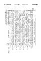
- FIGS. 9 through 12show alternative embodiments of the top layer etchant transmission openings or windows for fabrication of the free-space dielectric interconnect structure of the present invention.
- FIG. 9shows an array of square shaped holes.
- FIG. 10shows an array of circular holes.
- FIGS. 11 and 12show two different arrays of rectangular-shaped holes.
- FIG. 13depicts the interconnect structure of FIG. 8 following formation of the etchant-transmission window pattern on the top layer and after formation of the free-space dielectric medium for the purposes of illustrating one example of forming the free-space dielectric interconnect structure of the present invention
- FIG. 14shows the top dielectric layer after formation of the etchant transmission windows used to enable formation of the free-space dielectric medium, and also following the subsequent deposition steps for hermetic sealing of the interconnect structure of the present invention.
- FIG. 15shows the multi-level interconnect structure of the present invention after formation of the free-space dielectric medium, hermetically-sealed top layer, and the bonding pad windows.
- FIG. 4shows one example of a prior art interconnect process flow 40 that results in a dual-damascene multi-level copper metallization interconnect structure in conjunction with inorganic interlevel dielectric (ILD) and intermetal dielectric (IMD) layers (e.g., fluorinated oxide or Si x O y F z ILD/IMD material).
- ILDintermetal dielectric
- tungstenis used to form tungsten contact plugs (to keep copper away from silicon) while copper is used for all the via plugs.
- the interconnect fabrication process(or back-end-of-the-line or BEOL process) flow starts after completion of the front-end-of-the-line (FEOL) process flow utilized for fabrication of the transistor and isolation (and other devices such as diodes, capacitors, etc.) structures, as step 42 indicates.
- FEOLfront-end-of-the-line
- the first ILD layer(ILD1) which may be SiO 2 , Si x O y F z , or another material) is deposited, as shown in step 44, by thermal CVD or PECVD and then globally planarized by chemical-mechanical polishing (CMP) and cleaned after the CMP step at step 46. Subsequently, the complete ILD structure is formed by deposition using CVD or PECVD of an additional amount of the dielectric material (e.g., SiO 2 , Si x O y F z , or another suitable insulating material), as indicated in step 48. After formation of the contact holes by microlithography and reactive ion etching or RIE as shown in the liner/barrier layers (e.g.
- Ti/TiNare formed by PVD and/or CVD (see step 50, step 52). Then the tungsten contact plugs are formed by blanket deposition of a tungsten layer to fill the contact holes (see step 54) followed by tungsten CMP and post-CMP clean as shown in steps 54 and 56. The fabrication flow then continues by deposition of a relatively thick etch-stop layer (e.g. silicon nitride layer) followed by deposition of the second ILD layer (e.g., SiO 2 or Si x O y F z ).
- etch-stop layere.g. silicon nitride layer
- the second ILD layere.g., SiO 2 or Si x O y F z
- the metal-1 (first metal level) line trenchesfor subsequent formation of inlaid metal-1 interconnects, are formed by microlithography patterning and RIE (with the thin Si 3 N 4 etch-stop layer used for RIE process end-pointing) (step 60). Si 3 N 4 is also removed from the bottom of trenches by RIE.
- the RIE step used for removal of the silicon nitride layer at the bottom of the trenchesselectively removes the nitride layer and stops on ILD1.
- the diffusion barrier layer(TiN, Ta, TaN, or another suitable material) is deposited either by CVD or PVD (e.g., to form a 150 ⁇ to 300 ⁇ barrier layer) (step 62).
- the inlaid metal-1 interconnect linesare then formed by depositing copper (by MOCVD, PVD, and/or plating) followed by subsequent metal CMP and post-CMP clean through steps 64 and 66.
- the following dual-damascene copper interconnect levelis fabricated by depositing the intermetal dielectric (IMD) layer (e.g., a multi-layer dielectric comprising a thin silicon nitride dielectric barrier and etch-stop layer, followed by deposition of SiO 2 , a thin Si 3 N 4 etch-stop layer, and a top layer of silicon dioxide (SiO 2 ) layer; the oxide layers may be replaced by a reduced-permittivity material such as Si x O y F z ), as shown in step 68. Then, a microlithography patterning process and a reactive ion etch (RIE) process sequence is used (step 70) in order to form the dielectric trenches for subsequent formation of inlaid copper metal lines.
- IMDintermetal dielectric
- RIEreactive ion etch
- a follow-on microlithography patterning and dielectric RIE process sequenceis used to form the interconnect via holes (step 72).
- a diffusion barrier layerTiN, Ta, TaN, etc.
- CVD or PVDa diffusion barrier layer
- a copper layeris deposited, as shown in step 78, (by MOCVD, PVD and/or Plating) and polished back by CMP, followed by post-CMP clean (step 80) resulting in formation of the embedded copper via plugs and inlaid metal interconnect lines.
- the repeatitive steps of IMD deposition, microlithograhy patterning and dielectric RIE processes (for via holes and interconnect metal line trenches), as well as barrier and copper deposition steps, and CMP and post-CMP cleanare performed multiple times until all the necessary interconnect levels are fabricated, as verified at step 82.
- the passivation overlayere.g., Si 3 N 4 or SiON
- PECVDPECVD
- a microlithography patterning step and an RIE process stepare used (step 86), to form the bonding pad openings or windows.
- the chipcan then be packaged, as step 88 indicates.
- the process flowchart 90 of FIG. 5presents another example of a state-of-the-art prior art interconnect process technology for formation of dual-damascene copper metallization with advanced low-k (e.g., K ⁇ 2.5) IMD/ILD layers.
- Process flow 90is fairly similar to the prior art process flow of FIG. 4 except for additional process steps 92 and 94.
- the additional process steps 92 and 94 for integration of copper and low-k dielectricsare required in order to maintain good low-k dielectric integrity through the BEOL interconnect process flow and also to eliminate any process integration issues in terms of patterning and etch processes as well as any material compatibility issues.
- the description of the process flow outlined in FIG. 5is essentially similar to that already provided for the flowchart in FIG. 4. One difference is that a thin layer of a hard mask material (such as SiO 2 ) is used to protect the ILD or IMD low-k dielectric surface prior to any patterning and CMP process steps.
- a thin layer of a hard mask materialsuch
- the organic low-k dielectric materialsmay be damaged in typical plasma ash processes used for removal of the patterned photoresist layers after patterning and etch processes (thus, the reason for the use of an oxide hard mask). Moreover, many low-k organic dielectrics may not be directly exposed to the CMP pad and slurry due to possible damage or degradation of their properties. This is another reason for using the oxide hard mask to protect the low-k dielectric. Moreover, this process flow forms a thin layer of dielectric (e.g., oxide) liner on the sidewalls of the dielectric trenches and via holes in order to protect a low-k dielectric from plasma etching and also to provide a good sidewall surface for deposition of the barrier layer. For IMD layers, the multi-layer stack comprises Si 3 N 4 , low-k dielectric, thin SiO 2 , low-k dielectric, and thin SiO 2 .
- dielectrice.g., oxide
- the lower and upper low-k dielectric layershouse the via plugs and the inlaid interconnect metal lines on each level, respectively.
- the lower silicon nitride layer(thin nitride) is used as a dielectric diffusion barrier to encapsulate the lower level copper interconnect lines.
- the middle thin SiO 2 layeris used as an etch-stop layer during the formation of the metal trenches.
- the following discussionfocuses on the description of the interconnect process flows and structures of the present invention appearing in FIGS. 6 and 7. Two closely related preferred flows of invention (preferred process flow embodiments) are shown in the flowchart 100 of FIG. 6 and flowchart 150 of FIG. 7.
- the back-end-of-the-line (BEOL) interconnect process flowstarts after completion of the front-end-of-the-line (FEOL) fabrication process flow for the transistors, isolation regions, etc. (step 102).
- the next stepis to deposit a blanket layer of a suitable dielectric diffusion barrier material which is also highly resistant against typical etch chemistries (e.g., HF-based etchants) used for oxide etching.
- etch chemistriese.g., HF-based etchants
- a layer of silicon nitridee.g., 2000 ⁇ to 5000 ⁇ Si 3 N 4
- thermal CVDPECVD
- PVDPVD
- This layerwill serve as a dense etch-resistant layer used for protection of the active transistor devices and isolation structures during subsequent etching of the disposable inter-level and inter-metal oxide layers.
- this thick and dense etch-resistant dielectric barrier layerprevents any copper diffusion into the silicon substrate and active device regions during the BEOL interconnect processing.
- suitable dielectric materialse.g., AlN or diamond-like carbon or DLC may be used instead of Si 3 N 4 for this material layer.
- the first disposable interlevel dielectric (ILD 1 ) layeris deposited (step 106). This involves preferably a silicon dioxide layer to be deposited by CVD, PECVD, or even PVD at step 108.
- dielectric CMP and post-CMP cleaning processesare performed (step 108) to form a globally planarized dielectric surface. This will provide a globally planar wafer surface throughout the multilevel interconnect fabrication process flow.
- a multi-layer disposable dielectric stacke.g., SiO 2 /SiON/SiO 2
- CVDPECVD
- PVDPVD
- the stackincludes upper and lower silicon dioxide layers separated by a thin etch-stop (or etch end-point detection) layer of a different material such as silicon oxynitride (SION) or aluminum oxide (Al 2 O 3 ) or another suitable disposable material.
- etch-stopor etch end-point detection
- the thin intermediate layer of oxynitridewill be used an etch end-point marker during subsequent formation of the metal line trenches by anisotropic reactive-ion etching.
- a microlithography patterning process and subsequent dielectric RIE (anisotropic etching) processare performed, as shown at step 112, to form the contact holes.
- step 114another microlithography patterning process and an anisotrophic RIE process are used to form the dielectric trenches for the first level of metal interconnect lines (step 114).
- the first level metallizationis performed by sequential deposition of the barrier layer (e.g., Ta, TaN, WN x , or TiN by PVD or CVD) as shown in step 116, and a copper layer (by MoCVD, PVD, and/or plating), as indicated in step 118.
- barrier layere.g., Ta, TaN, WN x , or TiN by PVD or CVD
- a copper layerby MoCVD, PVD, and/or plating
- fabrication of the next interconnect levelproceeds by deposition of a suitable multi-layer disposable dielectric stack, preferably SiON/SiO 2 /SiON/SiO 2 , formed by CVD, PECVD, or PVD (step 122).
- a suitable multi-layer disposable dielectric stackpreferably SiON/SiO 2 /SiON/SiO 2 , formed by CVD, PECVD, or PVD (step 122).
- the silicon oxynitride (SiON) layersare relatively thin compared to the upper and lower SiO 2 layers (e.g., 100 ⁇ to 500 ⁇ ) and are used as etch-stop layers during subsequent RIE etch processes for formation of the via holes and metal line trenches.
- Other suitable materialssuch as aluminum oxide may be used instead of SiON as etch-stop layers.
- steps 124 and 126)two sequential steps of microlithography patterning and anisotropic RIE processes are performed for formation of the via holes and the interconnect metal line trenches.
- a layer of copperis deposited (step 128), by MOCVD, PVD, and/or plating to fill the via holes and interconnect metal line trenches. Note that at this stage copper can be deposited directly on the patterned structure without a need for a diffusion barrier layer, thus, simplifying the interconnect process flow.
- an adhesion promotion glue layermay be deposited on the surface prior to deposition of copper.
- copper CMP and post-CMP clean processesare performed, at step 130, in order to form the embedded via copper plugs and inlaid interconnect metal lines.
- the repetitive steps of multi-layer dielectric stack deposition, fabrication of via holes and metal line trenches, copper deposition, and copper CMP (and post-CMP clean)are performed multiple times until all the necessary interconnect levels are fabricated, as verified at step 132.
- a top etch-resistant dielectric layerpreferably a silicon nitride layer (on the order of 2000 ⁇ to 1 ⁇ m thick), is deposited by CVD, PECVD, or PVD, at step 134.
- FIG. 8illustrates the example of a cross-sectional view of a multi-level interconnect structure (shown with six levels of copper interconnect) at this stage in the interconnect fabrication process flow.
- a microlithography patterning process and a subsequent anisotropic RIE processare performed (see step 136) in order to form etchant transmission windows or openings within the top dielectric layer.
- the schematic diagrams on pages FIGS. 9, 10, 11 and 12show several possible layout patterns of the etchant transmission windows, formed within the top etch-resistant dielectric layer.
- the etchant transmission window patterncomprises openings or windows (squares, rectangular, circular, etc.) with at least one minimum-geometry in-plane dimension.
- the pattern of FIG. 9shows an array of closely-spaced square windows.
- FIG. 10For a 0.18 ⁇ m technology node, these windows may have 0.18 ⁇ m ⁇ 0.18 ⁇ m areas and the adjacent windows may be separated by 0.18 ⁇ m.
- the alternative pattern in FIG. 10comprises an array of circular holes. Again, the holes may have minimum-geometry diameters (e.g., 0.18 ⁇ m diametric dimensions for circular holes separated by 0.18 ⁇ m from each other in a 0.18 ⁇ m technology).
- FIGS. 10 and 11show two alternative etchant transmission window patterns comprising rectangular windows with larger overall transmission window area ratios (ratio of total area of the windows to the total surface area).
- the smaller side dimensions of these rectangular windowsare preferably the same as the resolution of the microlithography tool (e.g., 0.18 ⁇ m for a 0.18 ⁇ m technology), while the larger side dimensions (lengths of rectangular windows) may be several to tens to even hundreds of microns ( ⁇ m).
- the ideais to have an etchant transmission window pattern which provides a relatively large transmission area ratio (preferably a ⁇ 50%) and can be subsequently hermetically sealed using a simple deposition process without a significant impact on the interconnect metallization structure.
- the thickness of the top etch-resistant layere.g.
- Si 3 N 4 or AIN layer deposited by CVD, PECVD, or PVD or any other vapor deposition processis several times larger than the smaller side dimension of the etchant transmission unit cells.
- etchant transmission window cellssquare, circular, rectangular, or any other shape
- 0.18 ⁇ m minimum in-plane dimensione.g., rectangular unit cells, with 0.18 ⁇ m ⁇ 5 ⁇ m window size
- a highly selective etch(preferable a wet etch process such as HF-based etch) is performed at step 138 in order to selectively remove the entire multi-level disposable silicon dioxide dielectric structure.
- This etch chemistry and the resulting etch byproductseasily pass through the etchant transmission windows (or unit cells) facilitating the etch process.
- the selective etchantcan easily remove the entire multi-level oxide and oxynitride dielectric stack bound between the lower etch-resistant layer (e.g., silicon nitride or aluminum nitride or DLC) and the upper etch-resistant patterned (e.g., also silicon nitride, aluminum nitride, or DLC) layer.
- the selective etchante.g., HF-based wet etchant
- the selective etchantdoes not or should not attack the metallization structure and may remove only a very small fraction of the top and bottom etch-resistant layers (e.g., silicon nitride, aluminum nitride, or DLC).
- the preferenceis to use an etchant with sufficiently high selectivity (>100:1) to the disposable ILD/IMD materials compared to the etch-resistant material which limits the thickness removal of the top and bottom etch-resistant layers (e.g., silicon nitride or aluminum nitride or DLC or another suitable dielectric) to preferably ⁇ 1000 ⁇ .
- the schematic cross-sectional diagram of FIG. 13shows the resulting device structure after the selective removal of the disposable oxide dielectric layers. As shown, the multi-level copper interconnect structure is now surrounded by free-space medium within the structure between the top and bottom etch-resistant (e.g., silicon nitride) layers.
- the multi-level copper interconnect structureis mechanically supported by its own line and plug interconnections as well as the top and bottom boundary planes defined by the top and bottom etch-resistant silicon nitride layers which have sealed contacts to the top metal level and bottom contact plugs, respectively.
- a plurality of metallic columns made of stacked dummy contact and via plugsmay be used to provide additional mechanical support between the top and bottom etch-resistant layers (this is optional but not necessary.)
- step 140it is possible to perform an optional thermal anneal as shown at step 140 (e.g., at a temperature between 250° C. and 400° C.) in order to form large grains and preferred highly oriented texturing in the interconnect structure for improved electromigration lifetime, and enhanced metallization conductivity as well as to relieve any residual stresses.
- This optional thermal anneal processmay also be used to form a large-grain multi-level copper metallization system with "bamboo-type" microstructure for maximum electromigration lifetime reliability improvement.
- the first deposition processis a substantially conformal (CVD or PECVD) deposition process for deposition of a controlled thickness (e.g., 50 ⁇ to 200 ⁇ ) of a dielectric material such as SiO 2 , Si 3 N 4 , AlN, Al 2 O 3 , etc.
- the preferred materialis silicon dioxide.
- This conformal deposition processdeposits a thin (e.g., 50 ⁇ to 200 ⁇ ) layer of encapsulating dielectric material such as SiO 2 over all the exposed surface areas of the multi-level metallization structure (metal lines and plugs).
- This deposition processalso deposits a thin layer of the conformal dielectric over the exposed surfaces of the top etch-resistant patterned dielectric (e.g., silicon nitride), including the etchant transmission windows as well as a thin layer over the bottom etch-resistant layer.
- the amount of conformal dielectric thicknesscan be deliberately chosen to be small enough such that it is not sufficient to completely seal the etchant transmission windows or the top patterned etch-resistant insulator.
- the main purpose of this conformal dielectric (e.g., silicon dioxide) deposition stepis to prevent or suppress thermionic emission and/or low-voltage electrical breakdown between the adjacent intra-level and inter-level metal lines and/or plugs through the free-space medium.
- the second deposition stepis preferably a substantially nonconformal or directional deposition step (with poor step coverage) used to form a hermetically-sealed top insulating passivation overlayer.
- PVDplasma sputtering
- PECVDplasma sputtering
- other processessuch as jet-vapor deposition or laser ablation
- the deposited materialhas excellent diffusion barrier properties against ionic contamination and moisture, and also has a relatively high thermal conductivity.
- this nonconformal or directional depositionmay involve an atmospheric deposition process (preferably a thermal CVD process with helium carrier gas or an atmospheric laser ablation deposition process using a suitable target material in an inert atmosphere) for deposition of silicon nitride, aluminum nitride, DLC, or another suitable material.
- an atmospheric deposition processpreferably a thermal CVD process with helium carrier gas or an atmospheric laser ablation deposition process using a suitable target material in an inert atmosphere
- silicon nitridealuminum nitride, DLC, or another suitable material.
- the schematic diagrams shown in FIG. 14show an example of the evolution of the top dielectric layer starting from a patterned layer comprising etchant transmission windows and ending as a hermetically-sealed structure with fully sealed windows (the top and bottom figures show the cross-sectional diagrams of the top dielectric layer before and after the conformal/non-conformal dielectric deposition processes).
- Another practical process sequence for the hermetic sealing of the interconnect structureis as follows: (i) perform an atmospheric low-temperature silicon dioxide deposition (partially conformal) step using SiH 4 /N 2 O in a helium carrier gas in order to deposit a thin layer of oxide on the metallization structure and to seal the etchant transmission windows; (ii) Deposit a layer of silicon nitride (or silicon oxynitride) as passivation overlayer (this may be a ⁇ 5000 ⁇ thick layer deposited by PECVD); (iii) Deposit a layer (e.g., 5000 ⁇ to over 1 ⁇ m thick layer) of high-thermal conductivity insulating material, preferably aluminum nitride or DLC, by a suitable deposition process (preferably RF magnetron sputtering or PECVD).
- a suitable deposition processpreferably RF magnetron sputtering or PECVD
- This exemplary process sequenceresults in complete hermetic sealing of the chip interconnect structure by reproducing a continuous top passivation layer. Moreover, this process sequence results in a helium-filled free-space intermetal/interlevel dielectric medium.
- the atmospheric helium free-space dielectric mediumprovides an excellent heat transfer medium within the multi-level interconnect structure; it also further suppresses any thermionic emission (resulting in electrical leakage currents) or gas breakdown effects due to the intra-level and inter-level voltages between the adjacent metal lines and conductive plugs.
- the example aboveshows the typical process flow for formation of a hermetically-sealed continuous dielectric layer on the top in conjunction with a hermetically sealed helium-filled (e.g., at or near atmospheric pressure) free-space interlevel/intermetal dielectric medium.
- a hermetically sealed helium-filled (e.g., at or near atmospheric pressure) free-space interlevel/intermetal dielectric mediume.g., at or near atmospheric pressure) free-space interlevel/intermetal dielectric medium.
- the free-space helium pressurecan be increased to above atmospheric pressure (e.g., 1 to 5 atmospheres) by performing the directional deposition (e.g., laser ablation) process (see FIG. 14) in a pressurized process chamber filled with higher pressure helium.
- the preferred method and structure of this embodimentemploy atmospheric or near-atmospheric helium (or another suitable inert gas such as argon) to fill the sealed free space interconnect dielectric ILD/IMD volume.
- atmospheric or near-atmospheric heliumor another suitable inert gas such as argon
- Lower helium gas pressurese.g., 1 Torr to 1 atm.
- other types of gase.g., argon, nitrogen, hydrogen, etc.
- a gas-filled free-space dielectric regionis preferred over a near-vacuum free-space medium, both due to thermal management (efficient heat removal) and dielectric breakdown considerations.
- a helium-filled free-space medium 16(preferably at or near atmospheric He pressure) provides a much superior heat transfer medium (in conjunction with the high-thermal conductivity copper metallization structure as well as the high-thermal-conductivity top and bottom etch-resistant layers), a superior breakdown-resistant interconnect structure, and a better thermionic-emission-resistant free-space medium compared to a vacuum free-space medium.
- the next fabrication moduleis a microlithography patterning step (step 144), followed by an anisotropic dielectric RIE process in order to form the bonding pad windows by etching openings in the top passivation overlayer.
- the schematic diagram on FIG. 15shows the multi-level copper interconnect structure after this patterning and etch step.
- This structureincludes multi-level copper interconnects bound between the bottom dielectric diffusion barrier layer and the top high-thermal-conductivity hermetic sealing layer.
- the metallization structureis surrounded by a sealed free-space medium filled with an inert gas such as helium.
- the waferis ready for dicing and packaging, at step 146 (such as flip-chip packaging).
- the multi-level interconnect structureis fully hermetically sealed with an embedded free-space (preferably filled with He) ILD/IMD medium. This structure provides the highest level of interconnect electrical performance and reliability lifetime far superior to any interconnect structure comprising other low-k dielectric materials.
- the process flow of the preferred embodiment of the present inventionemploys one extra microlithography masking step for formation of the etchant transmission windows in the top etch-resistant layer.
- the process flow of FIG. 6shows that two separate masking steps are used for formation of the etchant transmission windows and the bonding pad windows (resulting in the need for one extra masking step).
- Process flow 150 of FIG. 7is essentially similar to the first embodiment (shown in FIG. 6) through the copper CMP and post-CMP cleaning processes for the last (topmost) level of copper interconnect, i.e. step 132.
- the top etch-resistant dielectric layer(or multi-layer material stack) is deposited by CVD, PVD, and/or PECVD, at step 134.
- a layer of dense silicon nitridee.g., 5000 ⁇ to ⁇ 1 ⁇ m thick
- a bi-layer of Si 3 N 4 /AlNe.g., 5000 ⁇ to over 1 ⁇ m silicon nitride followed by 5000 ⁇ to over 1 ⁇ m aluminum nitride
- PECVD and/or PVDa layer of dense silicon nitride
- Si 3 N 4 /AlNe.g., 5000 ⁇ to over 1 ⁇ m silicon nitride followed by 5000 ⁇ to over 1 ⁇ m aluminum nitride
- a microlithography patterning process and a subsequent anisotropic dielectric RIE processare performed sequentially to form the etchant transmission windows (corresponding to a suitable pattern such as one of those examples shown in FIGS. 9-12), and also the bonding pad windows at step 152.
- this masking stepcombines the layouts of the etchant transmission windows and the bonding pads into one micro
- the disposable silicon dioxide ILD/IMD layersare selectively removed using a highly selective wet etchant at step 138. This results in the multi-level interconnect structure with free-space ILD/IMD medium surrounding the intercconect structure.
- the copper metallization structureis coated with a controlled thin layer (e.g. 50 ⁇ to 200 ⁇ ) of silicon dioxide (or silicon nitride or another preferably insulating material) and the interconnect structure is hermetically sealed using the multi-step (e.g., two or three step) conformal/nonconformal dielectric deposition processes (step 142), as described in detail in association with FIG. 6.
- the next fabrication process stepis a blanket plasma (e.g., RIE) dielectric etch-back process until the bonding pads are re-exposed, at step 144.
- This etch-back processat step 144, can be easily endpointed using an optical etch end-point detection method (e.g., laser reflectance endpoint).
- the waferis diced into IC chips and the chips are packaged using a suitable packaging technology.
- the total number of microlithography masking step for an N-level interconnect structureis 2N+1, which is the same as the number of masks required in conventional prior art interconnect process flows.
- the first embodiment of this invention(shown in FIG. 6) employs 2N+2 microlithography masking steps.
Landscapes
- Engineering & Computer Science (AREA)
- Computer Hardware Design (AREA)
- Microelectronics & Electronic Packaging (AREA)
- Power Engineering (AREA)
- Physics & Mathematics (AREA)
- Condensed Matter Physics & Semiconductors (AREA)
- General Physics & Mathematics (AREA)
- Internal Circuitry In Semiconductor Integrated Circuit Devices (AREA)
Abstract
Description
Claims (35)
Priority Applications (7)
| Application Number | Priority Date | Filing Date | Title |
|---|---|---|---|
| US09/064,431US6016000A (en) | 1998-04-22 | 1998-04-22 | Ultra high-speed chip semiconductor integrated circuit interconnect structure and fabrication method using free-space dielectrics |
| US09/187,297US6124198A (en) | 1998-04-22 | 1998-11-05 | Ultra high-speed chip interconnect using free-space dielectrics |
| KR1019997012124AKR20010020476A (en) | 1998-04-22 | 1999-04-22 | Ultra high-speed chip interconnect using free-space dielectrics |
| PCT/US1999/008475WO1999054934A1 (en) | 1998-04-22 | 1999-04-22 | Ultra high-speed chip interconnect using free-space dielectrics |
| JP55318099AJP2002506577A (en) | 1998-04-22 | 1999-04-22 | Interconnection of ultra-high-speed chips using free-space dielectrics |
| EP99917606AEP1000440A1 (en) | 1998-04-22 | 1999-04-22 | Ultra high-speed chip interconnect using free-space dielectrics |
| US10/091,795US20040061229A1 (en) | 1998-04-22 | 2002-03-06 | Ultra high-speed chip semiconductor integrated circuit interconnect structure and fabrication method using free-space dielectrics |
Applications Claiming Priority (1)
| Application Number | Priority Date | Filing Date | Title |
|---|---|---|---|
| US09/064,431US6016000A (en) | 1998-04-22 | 1998-04-22 | Ultra high-speed chip semiconductor integrated circuit interconnect structure and fabrication method using free-space dielectrics |
Related Child Applications (2)
| Application Number | Title | Priority Date | Filing Date |
|---|---|---|---|
| US09/187,297DivisionUS6124198A (en) | 1998-04-22 | 1998-11-05 | Ultra high-speed chip interconnect using free-space dielectrics |
| US10/091,795DivisionUS20040061229A1 (en) | 1998-04-22 | 2002-03-06 | Ultra high-speed chip semiconductor integrated circuit interconnect structure and fabrication method using free-space dielectrics |
Publications (1)
| Publication Number | Publication Date |
|---|---|
| US6016000Atrue US6016000A (en) | 2000-01-18 |
Family
ID=22055931
Family Applications (2)
| Application Number | Title | Priority Date | Filing Date |
|---|---|---|---|
| US09/064,431Expired - Fee RelatedUS6016000A (en) | 1998-04-22 | 1998-04-22 | Ultra high-speed chip semiconductor integrated circuit interconnect structure and fabrication method using free-space dielectrics |
| US10/091,795AbandonedUS20040061229A1 (en) | 1998-04-22 | 2002-03-06 | Ultra high-speed chip semiconductor integrated circuit interconnect structure and fabrication method using free-space dielectrics |
Family Applications After (1)
| Application Number | Title | Priority Date | Filing Date |
|---|---|---|---|
| US10/091,795AbandonedUS20040061229A1 (en) | 1998-04-22 | 2002-03-06 | Ultra high-speed chip semiconductor integrated circuit interconnect structure and fabrication method using free-space dielectrics |
Country Status (1)
| Country | Link |
|---|---|
| US (2) | US6016000A (en) |
Cited By (131)
| Publication number | Priority date | Publication date | Assignee | Title |
|---|---|---|---|---|
| US6071805A (en)* | 1999-01-25 | 2000-06-06 | Chartered Semiconductor Manufacturing, Ltd. | Air gap formation for high speed IC processing |
| US6127258A (en)* | 1998-06-25 | 2000-10-03 | Motorola Inc. | Method for forming a semiconductor device |
| US6159857A (en)* | 1999-07-08 | 2000-12-12 | Taiwan Semiconductor Manufacturing Company | Robust post Cu-CMP IMD process |
| US6159787A (en)* | 1998-05-28 | 2000-12-12 | International Business Machines Corporation | Structures and processes for reduced topography trench capacitors |
| US6163074A (en)* | 1998-06-24 | 2000-12-19 | Samsung Electronics Co., Ltd. | Integrated circuit bonding pads including intermediate closed conductive layers having spaced apart insulating islands therein |
| US6202191B1 (en)* | 1999-06-15 | 2001-03-13 | International Business Machines Corporation | Electromigration resistant power distribution network |
| US6211068B1 (en)* | 1999-05-25 | 2001-04-03 | United Microelectronics Corp. | Dual damascene process for manufacturing interconnects |
| US6255712B1 (en)* | 1999-08-14 | 2001-07-03 | International Business Machines Corporation | Semi-sacrificial diamond for air dielectric formation |
| US6258715B1 (en)* | 1999-01-11 | 2001-07-10 | Taiwan Semiconductor Manufacturing Company | Process for low-k dielectric with dummy plugs |
| US6265304B1 (en)* | 1999-10-05 | 2001-07-24 | Advanced Micron Devices, Inc. | Controlling an etching process of multiple layers based upon thickness ratio of the dielectric layers |
| US6281113B1 (en)* | 1999-03-17 | 2001-08-28 | Canon Sales Co., Inc. | Method for forming an interplayer insulating film and semiconductor device |
| EP1130654A1 (en)* | 2000-03-01 | 2001-09-05 | Infineon Technologies AG | Integrated device including a metal- insulator-metal capacitor |
| US6302766B1 (en) | 1998-08-31 | 2001-10-16 | Cypress Semiconductor Corp. | System for cleaning a surface of a dielectric material |
| US6323556B2 (en)* | 1998-11-17 | 2001-11-27 | Nec Corporation | Interconnect structure of semiconductor device |
| US6348395B1 (en) | 2000-06-07 | 2002-02-19 | International Business Machines Corporation | Diamond as a polish-stop layer for chemical-mechanical planarization in a damascene process flow |
| US6350667B1 (en)* | 1999-11-01 | 2002-02-26 | Taiwan Semiconductor Manufacturing Company | Method of improving pad metal adhesion |
| US6361415B1 (en) | 1998-01-22 | 2002-03-26 | Cypress Semiconductor Corp. | Employing an acidic liquid and an abrasive surface to polish a semiconductor topography |
| US6368952B1 (en) | 2000-08-15 | 2002-04-09 | Taiwan Semiconductor Manufacturing Company, Ltd | Diffusion inhibited dielectric structure for diffusion enhanced conductor layer |
| US6380087B1 (en)* | 2000-06-19 | 2002-04-30 | Chartered Semiconductor Manufacturing Inc. | CMP process utilizing dummy plugs in damascene process |
| US6384486B2 (en)* | 1998-12-15 | 2002-05-07 | Texas Instruments Incorporated | Bonding over integrated circuits |
| WO2001078141A3 (en)* | 2000-04-11 | 2002-06-06 | Micron Technology Inc | USE OF AlN AS COPPER PASSIVATION LAYER AND THERMAL CONDUCTOR |
| US20020070419A1 (en)* | 2000-12-13 | 2002-06-13 | Farrar Paul A. | Method of forming buried conductor patterns by surface transformation of empty spaces in solid state materials |
| US6420189B1 (en)* | 2001-04-27 | 2002-07-16 | Advanced Micro Devices, Inc. | Superconducting damascene interconnected for integrated circuit |
| US20020100957A1 (en)* | 1999-06-10 | 2002-08-01 | Andreas Rusch | Configuration of fuses in semiconductor structures with Cu metallization |
| US20020113271A1 (en)* | 1999-08-10 | 2002-08-22 | Hitachi, Ltd. | Semiconductor integrated circuit device and manufacturing method of semiconductor integrated circuit device |
| US6451687B1 (en) | 2000-11-24 | 2002-09-17 | Chartered Semiconductor Manufacturing Ltd. | Intermetal dielectric layer for integrated circuits |
| US6468906B1 (en)* | 1998-12-28 | 2002-10-22 | Chartered Semiconductor Manufacturing Ltd. | Passivation of copper interconnect surfaces with a passivating metal layer |
| US20020160599A1 (en)* | 2001-03-27 | 2002-10-31 | Junichi Aoyama | Semiconductor device and wiring forming method in semiconductor device |
| US6482656B1 (en) | 2001-06-04 | 2002-11-19 | Advanced Micro Devices, Inc. | Method of electrochemical formation of high Tc superconducting damascene interconnect for integrated circuit |
| US20020171115A1 (en)* | 2001-05-17 | 2002-11-21 | Matsushita Electric Industrial Co., Ltd. | High frequency semiconductor device |
| US6495445B2 (en)* | 1999-07-02 | 2002-12-17 | International Business Machines Corporation | Semi-sacrificial diamond for air dielectric formation |
| US6514853B1 (en)* | 1999-06-25 | 2003-02-04 | Nec Corporation | Semiconductor device and a manufacturing process therefor |
| US20030051218A1 (en)* | 2001-09-07 | 2003-03-13 | Fujitsu Limited | Method for designing wiring connecting section and semiconductor device |
| US6545359B1 (en)* | 1998-12-18 | 2003-04-08 | Semiconductor Energy Laboratory Co., Ltd. | Wiring line and manufacture process thereof, and semiconductor device and manufacturing process thereof |
| US6552438B2 (en) | 1998-06-24 | 2003-04-22 | Samsung Electronics Co. | Integrated circuit bonding pads including conductive layers with arrays of unaligned spaced apart insulating islands therein and methods of forming same |
| US20030080436A1 (en)* | 2001-10-30 | 2003-05-01 | Semiconductor Energy Laboratory Co., Ltd. | Semiconductor device |
| US6560862B1 (en)* | 2001-02-06 | 2003-05-13 | Taiwan Semiconductor Manufacturing Company | Modified pad for copper/low-k |
| US6566249B1 (en)* | 1998-11-09 | 2003-05-20 | Cypress Semiconductor Corp. | Planarized semiconductor interconnect topography and method for polishing a metal layer to form wide interconnect structures |
| US20030127716A1 (en)* | 2002-01-09 | 2003-07-10 | Taiwan Semiconductor Manufacturing Co., Ltd. | Single layer wiring bond pad with optimum AL film thickness in Cu/FSG process for devices under pads |
| US6596624B1 (en)* | 1999-07-31 | 2003-07-22 | International Business Machines Corporation | Process for making low dielectric constant hollow chip structures by removing sacrificial dielectric material after the chip is joined to a chip carrier |
| US6599823B1 (en)* | 2000-10-24 | 2003-07-29 | United Microelectronics Corp. | Method for improving package bonding between multi-level interconnection lines and low K inter-metal dielectric |
| US20030197280A1 (en)* | 2002-02-15 | 2003-10-23 | International Business Machines Corporation | Unique feature design enabling structural integrity for advanced low K semiconductor chips |
| US6696360B2 (en)* | 2001-03-15 | 2004-02-24 | Micron Technology, Inc. | Barrier-metal-free copper damascene technology using atomic hydrogen enhanced reflow |
| US20040038073A1 (en)* | 2001-12-19 | 2004-02-26 | Chebiam Ramanan V. | Electroless plating bath composition and method of using |
| US20040036131A1 (en)* | 2002-08-23 | 2004-02-26 | Micron Technology, Inc. | Electrostatic discharge protection devices having transistors with textured surfaces |
| US20040041268A1 (en)* | 2002-06-07 | 2004-03-04 | Stmicroelectronics S.R.I. | Multilayer metal structure of supply rings with large parasitic capacitance |
| US20040061229A1 (en)* | 1998-04-22 | 2004-04-01 | Moslehi Mehrdad M. | Ultra high-speed chip semiconductor integrated circuit interconnect structure and fabrication method using free-space dielectrics |
| US6723634B1 (en)* | 2002-03-14 | 2004-04-20 | Advanced Micro Devices, Inc. | Method of forming interconnects with improved barrier layer adhesion |
| US6727590B2 (en)* | 2001-11-01 | 2004-04-27 | Renesas Technology Corp. | Semiconductor device with internal bonding pad |
| US20040105207A1 (en)* | 2002-08-09 | 2004-06-03 | Leopard Logic, Inc. | Via programmable gate array interconnect architecture |
| US6767839B1 (en)* | 1998-08-27 | 2004-07-27 | Tokyo Ohka Kogyo Co., Ltd. | Method for forming multi-layer wiring structure |
| US20040169213A1 (en)* | 2000-01-18 | 2004-09-02 | Micron Technology, Inc. | Integrated circuit and seed layers |
| US6804810B1 (en)* | 2000-02-21 | 2004-10-12 | Hewlett-Packard Development Company, L.P. | Resistance and capacitance estimation |
| US20040217481A1 (en)* | 2000-01-18 | 2004-11-04 | Micron Technology, Inc. | Structures and methods to enhance copper metallization |
| US20040242435A1 (en)* | 2003-05-29 | 2004-12-02 | Nissan Motor Co., Ltd. | Hard-carbon coated machine tool and cutting oil composition therefor |
| US20040241448A1 (en)* | 2003-05-27 | 2004-12-02 | Nissan Motor Co., Ltd. | Rolling element |
| US6828678B1 (en) | 2002-03-29 | 2004-12-07 | Silicon Magnetic Systems | Semiconductor topography with a fill material arranged within a plurality of valleys associated with the surface roughness of the metal layer |
| US20050005892A1 (en)* | 2003-05-23 | 2005-01-13 | Nissan Motor Co., Ltd. | Piston for internal combustion engine |
| US6849946B2 (en) | 1998-08-31 | 2005-02-01 | Cypress Semiconductor Corp. | Planarized semiconductor interconnect topography and method for polishing a metal layer to form interconnect |
| US20050025975A1 (en)* | 2003-07-31 | 2005-02-03 | Nissan Motor Co., Ltd. | Gear |
| US20050029501A1 (en)* | 2002-03-25 | 2005-02-10 | Micron Technology, Inc. | Low k interconnect dielectric using surface transformation |
| US20050037879A1 (en)* | 2003-08-13 | 2005-02-17 | Nissan Motor Co., Ltd. | Chain drive system |
| US20050035222A1 (en)* | 2003-04-15 | 2005-02-17 | Nissan Motor Co., Ltd. | Fuel injection valve |
| US20050056241A1 (en)* | 2003-08-08 | 2005-03-17 | Nissan Motor Co., Ltd. | Valve train for internal combustion engine |
| US20050064196A1 (en)* | 2003-08-21 | 2005-03-24 | Jean Martin | Low-friction sliding member and low-friction sliding mechanism using same |
| US20050070036A1 (en)* | 2001-05-16 | 2005-03-31 | Geusic Joseph E. | Method of forming mirrors by surface transformation of empty spaces in solid state materials |
| US6876076B2 (en)* | 2001-06-28 | 2005-04-05 | Stmicroelectronics Sa | Multilayer semiconductor device for transmitting microwave signals and associated methods |
| US6879015B2 (en)* | 2000-04-12 | 2005-04-12 | Koninklijke Philips Electronics N.V. | Semiconductor device with isolated intermetal dielectrics |
| US6887790B1 (en)* | 2002-07-19 | 2005-05-03 | Taiwan Semiconductor Manufacturing Company, Ltd. | Method of forming dummy copper plug to improve low k structure mechanical strength and plug fill uniformity |
| US20050100701A1 (en)* | 2003-08-08 | 2005-05-12 | Nissan Motor Co., Ltd. | Sliding member and production process thereof |
| US20050118426A1 (en)* | 1999-04-09 | 2005-06-02 | Shojiro Miyake | Slidably movable member and method of producing same |
| US20050208757A1 (en)* | 1998-12-21 | 2005-09-22 | Mou-Shiung Lin | Top layers of metal for high performance IC's |
| US20050213854A1 (en)* | 2002-11-06 | 2005-09-29 | Nissan Motor Co., Ltd. | Low-friction sliding mechanism |
| US20050258466A1 (en)* | 2004-05-24 | 2005-11-24 | Won-Kyu Kwak | Capacitor and light emitting display using the same |
| US6969684B1 (en) | 2001-04-30 | 2005-11-29 | Cypress Semiconductor Corp. | Method of making a planarized semiconductor structure |
| US20050285280A1 (en)* | 2004-06-25 | 2005-12-29 | Sin-Him Yau | Electrostatic discharge (ESD) protection for integrated circuit packages |
| US20060006548A1 (en)* | 2003-08-05 | 2006-01-12 | Micron Technology, Inc. | H2 plasma treatment |
| US20060138708A1 (en)* | 2002-01-17 | 2006-06-29 | Micron Technology, Inc. | Cellular materials formed using surface transformation |
| US20060226015A1 (en)* | 2003-02-04 | 2006-10-12 | Microfabrica Inc. | Method of forming electrically isolated structures using thin dielectric coatings |
| US20060246733A1 (en)* | 2000-01-18 | 2006-11-02 | Micron Technology, Inc. | Method for making integrated circuits |
| US7134381B2 (en) | 2003-08-21 | 2006-11-14 | Nissan Motor Co., Ltd. | Refrigerant compressor and friction control process therefor |
| US20060263604A1 (en)* | 2003-08-06 | 2006-11-23 | Martin Jean M | Low-friction sliding mechanism, low-friction agent composition and method of friction reduction |
| US20070045781A1 (en)* | 2005-08-26 | 2007-03-01 | Innovative Micro Technology | Hermetic interconnect structure and method of manufacture |
| US7228786B2 (en) | 2003-06-06 | 2007-06-12 | Nissan Motor Co., Ltd. | Engine piston-pin sliding structure |
| US20070132096A1 (en)* | 2005-12-08 | 2007-06-14 | Matsushita Electric Industrial Co., Ltd. | Semiconductor device and method of manufacturing the same |
| US20070143721A1 (en)* | 2004-11-08 | 2007-06-21 | International Business Machines Corporation | System and method for plasma induced modification and improvement of critical dimension uniformity |
| US7255083B2 (en) | 2002-10-16 | 2007-08-14 | Nissan Motor Co., Ltd. | Sliding structure for automotive engine |
| KR100752026B1 (en)* | 2001-09-07 | 2007-08-28 | 후지쯔 가부시끼가이샤 | Semiconductor device capable of suppressing current concentration in pad and its manufacture method |
| US7284525B2 (en) | 2003-08-13 | 2007-10-23 | Nissan Motor Co., Ltd. | Structure for connecting piston to crankshaft |
| US7318514B2 (en) | 2003-08-22 | 2008-01-15 | Nissan Motor Co., Ltd. | Low-friction sliding member in transmission, and transmission oil therefor |
| US20080029819A1 (en)* | 2006-08-04 | 2008-02-07 | Seiko Epson Corporation | Semiconductor device |
| US20080054483A1 (en)* | 2006-08-29 | 2008-03-06 | Lee John K | Semiconductor devices including fine pitch arrays with staggered contacts and methods for designing and fabricating the same |
| US20080116581A1 (en)* | 2003-10-15 | 2008-05-22 | Megica Corporation | Post passivation interconnection schemes on top of the ic chips |
| US7405149B1 (en)* | 1998-12-21 | 2008-07-29 | Megica Corporation | Post passivation method for semiconductor chip or wafer |
| US20080191352A1 (en)* | 2007-02-13 | 2008-08-14 | Chen-Hua Yu | Stacked contact with low aspect ratio |
| US20080251924A1 (en)* | 2003-10-15 | 2008-10-16 | Megica Corporation | Post Passivation Interconnection Schemes On Top Of The IC Chips |
| US7453158B2 (en) | 2003-07-31 | 2008-11-18 | Nvidia Corporation | Pad over active circuit system and method with meshed support structure |
| US20080296741A1 (en)* | 2007-05-30 | 2008-12-04 | Mitsubishi Electric Corporation | Semiconductor device |
| US20080316662A1 (en)* | 2007-06-21 | 2008-12-25 | Xiang Yin Zeng | Reducing input capacitance for high speed integrated circuits |
| US20090014773A1 (en)* | 2007-07-10 | 2009-01-15 | Ching-Nan Hsiao | Two bit memory structure and method of making the same |
| US7495343B1 (en) | 2003-07-31 | 2009-02-24 | Nvidia Corporation | Pad over active circuit system and method with frame support structure |
| US7670469B2 (en) | 2000-01-18 | 2010-03-02 | Micron Technology, Inc. | Methods and apparatus for making integrated-circuit wiring from copper, silver, gold, and other metals |
| US20100285654A1 (en)* | 2005-01-12 | 2010-11-11 | Samsung Electronics Co., Ltd. | Semiconductor device having reduced die-warpage and method of manufacturing the same |
| US20100314689A1 (en)* | 2009-06-11 | 2010-12-16 | International Business Machines Corporation | Local metallization and use thereof in semiconductor devices |
| US20110079922A1 (en)* | 2009-10-07 | 2011-04-07 | Taiwan Semiconductor Manufacturing Co., Ltd. | Integrated circuit with protective structure, and method of fabricating the integrated circuit |
| US20110132767A1 (en)* | 2003-02-04 | 2011-06-09 | Microfabrica Inc. | Multi-Layer, Multi-Material Fabrication Methods for Producing Micro-Scale and Millimeter-Scale Devices with Enhanced Electrical and/or Mechanical Properties |
| US20120122312A1 (en)* | 2010-11-17 | 2012-05-17 | King Sean W | Methods for forming planarized hermetic barrier layers and structures formed thereby |
| US8304907B2 (en) | 1998-12-21 | 2012-11-06 | Megica Corporation | Top layers of metal for integrated circuits |
| US20140362267A1 (en)* | 2011-07-05 | 2014-12-11 | Sony Corporation | Semiconductor device, fabrication method for a semiconductor device and electronic apparatus |
| TWI487090B (en)* | 2006-05-25 | 2015-06-01 | Renesas Electronics Corp | Semiconductor device |
| US20150162448A1 (en)* | 2013-12-10 | 2015-06-11 | Imec Vzw | Integrated circuit device with power gating switch in back end of line |
| US9196591B2 (en)* | 2014-02-17 | 2015-11-24 | International Business Machines Corporation | Chip with shelf life |
| US9245846B2 (en) | 2014-05-06 | 2016-01-26 | International Business Machines Corporation | Chip with programmable shelf life |
| US9546431B2 (en) | 2003-06-27 | 2017-01-17 | Microfabrica Inc. | Electrochemical fabrication methods incorporating dielectric materials and/or using dielectric substrates |
| US20170086294A1 (en)* | 2015-09-18 | 2017-03-23 | HGST Netherlands B.V. | Low Permeability Electrical Feed-Through |
| US9653399B2 (en)* | 2015-02-13 | 2017-05-16 | Qualcomm Incorporated | Middle-of-line integration methods and semiconductor devices |
| US9671429B2 (en) | 2003-05-07 | 2017-06-06 | University Of Southern California | Multi-layer, multi-material micro-scale and millimeter-scale devices with enhanced electrical and/or mechanical properties |
| US9741918B2 (en) | 2013-10-07 | 2017-08-22 | Hypres, Inc. | Method for increasing the integration level of superconducting electronics circuits, and a resulting circuit |
| US10128267B2 (en) | 2016-12-20 | 2018-11-13 | Samsung Electronics Co., Ltd. | Non-volatile memory device |
| US10395694B1 (en) | 2017-08-09 | 2019-08-27 | Western Digital Technologies, Inc. | Low permeability electrical feed-through |
| US20190288191A1 (en)* | 2017-03-07 | 2019-09-19 | International Business Machines Corporation | Selective growth of seed layer for magneto-resistive random access memory |
| US10424345B1 (en) | 2018-06-11 | 2019-09-24 | Western Digital Technologies, Inc. | Misalignment-tolerant flexible type electrical feed-through |
| US10594100B1 (en) | 2018-06-11 | 2020-03-17 | Western Digital Technologies, Inc. | Flexible type electrical feed-through connector assembly |
| US10629244B1 (en) | 2018-11-07 | 2020-04-21 | Western Digital Technologies, Inc. | Sealed electrical feed-through having reduced leak rate |
| US10641792B2 (en) | 2003-12-31 | 2020-05-05 | University Of Southern California | Multi-layer, multi-material micro-scale and millimeter-scale devices with enhanced electrical and/or mechanical properties |
| US10877067B2 (en) | 2003-02-04 | 2020-12-29 | Microfabrica Inc. | Pin-type probes for contacting electronic circuits and methods for making such probes |
| CN112299362A (en)* | 2019-07-25 | 2021-02-02 | 台湾积体电路制造股份有限公司 | Micro-electro-mechanical system device and forming method thereof |
| US20210125861A1 (en)* | 2019-10-29 | 2021-04-29 | Micron Technology, Inc. | Methods of forming microelectronic devices, and related microelectronic devices, and electronic systems |
| US11164778B2 (en) | 2019-11-25 | 2021-11-02 | International Business Machines Corporation | Barrier-free vertical interconnect structure |
| US11262383B1 (en) | 2018-09-26 | 2022-03-01 | Microfabrica Inc. | Probes having improved mechanical and/or electrical properties for making contact between electronic circuit elements and methods for making |
| US12078657B2 (en) | 2019-12-31 | 2024-09-03 | Microfabrica Inc. | Compliant pin probes with extension springs, methods for making, and methods for using |
Families Citing this family (18)
| Publication number | Priority date | Publication date | Assignee | Title |
|---|---|---|---|---|
| US6437441B1 (en)* | 1997-07-10 | 2002-08-20 | Kawasaki Microelectronics, Inc. | Wiring structure of a semiconductor integrated circuit and a method of forming the wiring structure |
| JP4574145B2 (en)* | 2002-09-13 | 2010-11-04 | ローム・アンド・ハース・エレクトロニック・マテリアルズ,エル.エル.シー. | Air gap formation |
| US7018918B2 (en)* | 2002-11-21 | 2006-03-28 | Intel Corporation | Method of forming a selectively converted inter-layer dielectric using a porogen material |
| US6943121B2 (en)* | 2002-11-21 | 2005-09-13 | Intel Corporation | Selectively converted inter-layer dielectric |
| US7371427B2 (en)* | 2003-05-20 | 2008-05-13 | Applied Materials, Inc. | Reduction of hillocks prior to dielectric barrier deposition in Cu damascene |
| US7723228B2 (en)* | 2003-05-20 | 2010-05-25 | Applied Materials, Inc. | Reduction of hillocks prior to dielectric barrier deposition in Cu damascene |
| US7474000B2 (en)* | 2003-12-05 | 2009-01-06 | Sandisk 3D Llc | High density contact to relaxed geometry layers |
| US7279424B2 (en)* | 2004-08-27 | 2007-10-09 | Hitachi Global Storage Technologies Netherlands B.V. | Method for fabricating thin film magnetic heads using CMP with polishing stop layer |
| US7176119B2 (en)* | 2004-09-20 | 2007-02-13 | International Business Machines Corporation | Method of fabricating copper damascene and dual damascene interconnect wiring |
| JP2006140326A (en)* | 2004-11-12 | 2006-06-01 | Toshiba Corp | Semiconductor device |
| US7309653B2 (en)* | 2005-02-24 | 2007-12-18 | International Business Machines Corporation | Method of forming damascene filament wires and the structure so formed |
| US7666787B2 (en)* | 2006-02-21 | 2010-02-23 | International Business Machines Corporation | Grain growth promotion layer for semiconductor interconnect structures |
| TWI290777B (en)* | 2006-02-27 | 2007-12-01 | Guei-Fang Chen | Lighting device with light emitting diode |
| KR101616044B1 (en)* | 2009-07-03 | 2016-04-28 | 삼성전자주식회사 | Semiconductor device comprising landing pad formed by electroless plating |
| US9018108B2 (en) | 2013-01-25 | 2015-04-28 | Applied Materials, Inc. | Low shrinkage dielectric films |
| US9135389B2 (en)* | 2013-09-25 | 2015-09-15 | United Microelectronics Corporation | Clock skew adjusting method and structure |
| US9941241B2 (en)* | 2016-06-30 | 2018-04-10 | International Business Machines Corporation | Method for wafer-wafer bonding |
| US10937735B2 (en) | 2018-09-20 | 2021-03-02 | International Business Machines Corporation | Hybrid under-bump metallization component |
Citations (10)
| Publication number | Priority date | Publication date | Assignee | Title |
|---|---|---|---|---|
| US3890636A (en)* | 1971-09-09 | 1975-06-17 | Hitachi Ltd | Multilayer wiring structure of integrated circuit and method of producing the same |
| US4289846A (en)* | 1979-12-28 | 1981-09-15 | General Electric Company | Process for forming low-reactance interconnections on semiconductors |
| US4933743A (en)* | 1989-03-11 | 1990-06-12 | Fairchild Semiconductor Corporation | High performance interconnect system for an integrated circuit |
| EP0475646A2 (en)* | 1990-09-12 | 1992-03-18 | Plessey Semiconductors Limited | Semiconductor integrated circuit comprising interconnections |
| US5117276A (en)* | 1989-08-14 | 1992-05-26 | Fairchild Camera And Instrument Corp. | High performance interconnect system for an integrated circuit |
| US5256869A (en)* | 1992-06-30 | 1993-10-26 | Texas Instruments Incorporated | Free-space optical interconnection using deformable mirror device |
| US5372969A (en)* | 1991-12-31 | 1994-12-13 | Texas Instruments Incorporated | Low-RC multi-level interconnect technology for high-performance integrated circuits |
| EP0644443A1 (en)* | 1993-09-16 | 1995-03-22 | Hitachi, Ltd. | Three-dimensional opto-electric integrated circuit using optical wiring |
| US5641712A (en)* | 1995-08-07 | 1997-06-24 | Motorola, Inc. | Method and structure for reducing capacitance between interconnect lines |
| US5798559A (en)* | 1996-03-29 | 1998-08-25 | Vlsi Technology, Inc. | Integrated circuit structure having an air dielectric and dielectric support pillars |
Family Cites Families (13)
| Publication number | Priority date | Publication date | Assignee | Title |
|---|---|---|---|---|
| JPH02220464A (en)* | 1989-02-22 | 1990-09-03 | Toshiba Corp | Semiconductor device and its manufacturing method |
| US5414221A (en)* | 1991-12-31 | 1995-05-09 | Intel Corporation | Embedded ground plane and shielding structures using sidewall insulators in high frequency circuits having vias |
| US5366911A (en)* | 1994-05-11 | 1994-11-22 | United Microelectronics Corporation | VLSI process with global planarization |
| DE4441898C1 (en)* | 1994-11-24 | 1996-04-04 | Siemens Ag | Semiconductor component with electrically conductive contacts and/or tracks |
| US5847464A (en)* | 1995-09-27 | 1998-12-08 | Sgs-Thomson Microelectronics, Inc. | Method for forming controlled voids in interlevel dielectric |
| US5900668A (en)* | 1995-11-30 | 1999-05-04 | Advanced Micro Devices, Inc. | Low capacitance interconnection |
| US5953626A (en)* | 1996-06-05 | 1999-09-14 | Advanced Micro Devices, Inc. | Dissolvable dielectric method |
| US6124198A (en)* | 1998-04-22 | 2000-09-26 | Cvc, Inc. | Ultra high-speed chip interconnect using free-space dielectrics |
| US6016000A (en)* | 1998-04-22 | 2000-01-18 | Cvc, Inc. | Ultra high-speed chip semiconductor integrated circuit interconnect structure and fabrication method using free-space dielectrics |
| US6207553B1 (en)* | 1999-01-26 | 2001-03-27 | Advanced Micro Devices, Inc. | Method of forming multiple levels of patterned metallization |
| US6667552B1 (en)* | 1999-02-18 | 2003-12-23 | Advanced Micro Devices, Inc. | Low dielectric metal silicide lined interconnection system |
| JP3481222B2 (en)* | 2001-09-07 | 2003-12-22 | 松下電器産業株式会社 | Wiring structure and its design method |
| US6713835B1 (en)* | 2003-05-22 | 2004-03-30 | International Business Machines Corporation | Method for manufacturing a multi-level interconnect structure |
- 1998
- 1998-04-22USUS09/064,431patent/US6016000A/ennot_activeExpired - Fee Related
- 2002
- 2002-03-06USUS10/091,795patent/US20040061229A1/ennot_activeAbandoned
Patent Citations (10)
| Publication number | Priority date | Publication date | Assignee | Title |
|---|---|---|---|---|
| US3890636A (en)* | 1971-09-09 | 1975-06-17 | Hitachi Ltd | Multilayer wiring structure of integrated circuit and method of producing the same |
| US4289846A (en)* | 1979-12-28 | 1981-09-15 | General Electric Company | Process for forming low-reactance interconnections on semiconductors |
| US4933743A (en)* | 1989-03-11 | 1990-06-12 | Fairchild Semiconductor Corporation | High performance interconnect system for an integrated circuit |
| US5117276A (en)* | 1989-08-14 | 1992-05-26 | Fairchild Camera And Instrument Corp. | High performance interconnect system for an integrated circuit |
| EP0475646A2 (en)* | 1990-09-12 | 1992-03-18 | Plessey Semiconductors Limited | Semiconductor integrated circuit comprising interconnections |
| US5372969A (en)* | 1991-12-31 | 1994-12-13 | Texas Instruments Incorporated | Low-RC multi-level interconnect technology for high-performance integrated circuits |
| US5256869A (en)* | 1992-06-30 | 1993-10-26 | Texas Instruments Incorporated | Free-space optical interconnection using deformable mirror device |
| EP0644443A1 (en)* | 1993-09-16 | 1995-03-22 | Hitachi, Ltd. | Three-dimensional opto-electric integrated circuit using optical wiring |
| US5641712A (en)* | 1995-08-07 | 1997-06-24 | Motorola, Inc. | Method and structure for reducing capacitance between interconnect lines |
| US5798559A (en)* | 1996-03-29 | 1998-08-25 | Vlsi Technology, Inc. | Integrated circuit structure having an air dielectric and dielectric support pillars |
Non-Patent Citations (2)
| Title |
|---|
| Solid State, by Linda Gepperts, IEEE Spectrum, Jan. 1998, pp. 23 28.* |
| Solid State, by Linda Gepperts, IEEE Spectrum, Jan. 1998, pp. 23-28. |
Cited By (290)
| Publication number | Priority date | Publication date | Assignee | Title |
|---|---|---|---|---|
| US6361415B1 (en) | 1998-01-22 | 2002-03-26 | Cypress Semiconductor Corp. | Employing an acidic liquid and an abrasive surface to polish a semiconductor topography |
| US20040061229A1 (en)* | 1998-04-22 | 2004-04-01 | Moslehi Mehrdad M. | Ultra high-speed chip semiconductor integrated circuit interconnect structure and fabrication method using free-space dielectrics |
| US6159787A (en)* | 1998-05-28 | 2000-12-12 | International Business Machines Corporation | Structures and processes for reduced topography trench capacitors |
| US6352902B1 (en) | 1998-05-28 | 2002-03-05 | International Business Machines Corporation | Process of forming a capacitor on a substrate |
| US6552438B2 (en) | 1998-06-24 | 2003-04-22 | Samsung Electronics Co. | Integrated circuit bonding pads including conductive layers with arrays of unaligned spaced apart insulating islands therein and methods of forming same |
| US6163074A (en)* | 1998-06-24 | 2000-12-19 | Samsung Electronics Co., Ltd. | Integrated circuit bonding pads including intermediate closed conductive layers having spaced apart insulating islands therein |
| US6465337B1 (en) | 1998-06-24 | 2002-10-15 | Samsung Electronics Co., Ltd. | Methods of fabricating integrated circuit bonding pads including intermediate closed conductive layers having spaced apart insulating islands therein |
| US6127258A (en)* | 1998-06-25 | 2000-10-03 | Motorola Inc. | Method for forming a semiconductor device |
| US6372665B1 (en) | 1998-06-25 | 2002-04-16 | Motorola Inc. | Method for forming a semiconductor device |
| US6767839B1 (en)* | 1998-08-27 | 2004-07-27 | Tokyo Ohka Kogyo Co., Ltd. | Method for forming multi-layer wiring structure |
| US6302766B1 (en) | 1998-08-31 | 2001-10-16 | Cypress Semiconductor Corp. | System for cleaning a surface of a dielectric material |
| US6849946B2 (en) | 1998-08-31 | 2005-02-01 | Cypress Semiconductor Corp. | Planarized semiconductor interconnect topography and method for polishing a metal layer to form interconnect |
| US6566249B1 (en)* | 1998-11-09 | 2003-05-20 | Cypress Semiconductor Corp. | Planarized semiconductor interconnect topography and method for polishing a metal layer to form wide interconnect structures |
| US20030219975A1 (en)* | 1998-11-09 | 2003-11-27 | Cypress Semiconductor Corporation | Planarized semiconductor interconnect topography and method for polishing a metal layer to form wide interconnect structures |
| US6323556B2 (en)* | 1998-11-17 | 2001-11-27 | Nec Corporation | Interconnect structure of semiconductor device |
| US6384486B2 (en)* | 1998-12-15 | 2002-05-07 | Texas Instruments Incorporated | Bonding over integrated circuits |
| US6545359B1 (en)* | 1998-12-18 | 2003-04-08 | Semiconductor Energy Laboratory Co., Ltd. | Wiring line and manufacture process thereof, and semiconductor device and manufacturing process thereof |
| US6809021B2 (en) | 1998-12-18 | 2004-10-26 | Semiconductor Energy Laboratory Co., Ltd. | Wiring line and manufacture process thereof and semiconductor device and manufacturing process thereof |
| US7420211B2 (en) | 1998-12-18 | 2008-09-02 | Semiconductor Energy Laboratory Co., Ltd. | Wiring line and manufacture process thereof, and semiconductor device and manufacturing process thereof |
| US20030132523A1 (en)* | 1998-12-18 | 2003-07-17 | Semiconductor Energy Laboratory Co., Ltd. | Wiring line and manufacture process thereof and semiconductor device and manufacturing process thereof |
| US7397135B2 (en) | 1998-12-21 | 2008-07-08 | Mou-Shiung Lin | Top layers of metal for high performance IC's |
| US7372155B2 (en)* | 1998-12-21 | 2008-05-13 | Mou-Shiung Lin | Top layers of metal for high performance IC's |
| US8022546B2 (en) | 1998-12-21 | 2011-09-20 | Megica Corporation | Top layers of metal for high performance IC's |
| US7884479B2 (en) | 1998-12-21 | 2011-02-08 | Megica Corporation | Top layers of metal for high performance IC's |
| US7863654B2 (en) | 1998-12-21 | 2011-01-04 | Megica Corporation | Top layers of metal for high performance IC's |
| US7482693B2 (en) | 1998-12-21 | 2009-01-27 | Mou-Shiung Lin | Top layers of metal for high performance IC's |
| US20050208757A1 (en)* | 1998-12-21 | 2005-09-22 | Mou-Shiung Lin | Top layers of metal for high performance IC's |
| US7465975B2 (en) | 1998-12-21 | 2008-12-16 | Mou-Shiung Lin | Top layers of metal for high performance IC's |
| US7456100B2 (en) | 1998-12-21 | 2008-11-25 | Mou-Shiung Lin | Top layers of metal for high performance IC's |
| US7442969B2 (en) | 1998-12-21 | 2008-10-28 | Mou-Shiung Lin | Top layers of metal for high performance IC's |
| US20080246154A1 (en)* | 1998-12-21 | 2008-10-09 | Megica Corporation | Top layers of metal for high performance IC's |
| US8022545B2 (en) | 1998-12-21 | 2011-09-20 | Megica Corporation | Top layers of metal for high performance IC's |
| US20070262460A1 (en)* | 1998-12-21 | 2007-11-15 | Mou-Shiung Lin | Top layers of metal for high performance IC's |
| US7425764B2 (en) | 1998-12-21 | 2008-09-16 | Mou-Shiung Lin | Top layers of metal for high performance IC's |
| US8304907B2 (en) | 1998-12-21 | 2012-11-06 | Megica Corporation | Top layers of metal for integrated circuits |
| US7405149B1 (en)* | 1998-12-21 | 2008-07-29 | Megica Corporation | Post passivation method for semiconductor chip or wafer |
| US8350386B2 (en) | 1998-12-21 | 2013-01-08 | Megica Corporation | Top layers of metal for high performance IC's |
| US20070267714A1 (en)* | 1998-12-21 | 2007-11-22 | Mou-Shiung Lin | Top layers of metal for high performance IC's |
| US7396756B2 (en) | 1998-12-21 | 2008-07-08 | Mou-Shiung Lin | Top layers of metal for high performance IC's |
| US7388292B2 (en) | 1998-12-21 | 2008-06-17 | Mou-Shiung Lin | Top layers of metal for high performance IC's |
| US20070273032A1 (en)* | 1998-12-21 | 2007-11-29 | Mou-Shiung Lin | Top layers of metal for high performance IC's |
| US7385292B2 (en) | 1998-12-21 | 2008-06-10 | Mou-Shiung Lin | Top layers of metal for high performance IC's |
| US8415800B2 (en) | 1998-12-21 | 2013-04-09 | Megica Corporation | Top layers of metal for high performance IC's |
| US20070273034A1 (en)* | 1998-12-21 | 2007-11-29 | Mou-Shiung Lin | Top layers of metal for high performance IC's |
| US7385291B2 (en) | 1998-12-21 | 2008-06-10 | Mou-Shiung Lin | Top layers of metal for high performance IC's |
| US7382058B2 (en) | 1998-12-21 | 2008-06-03 | Mou-Shiung Lin | Top layers of metal for high performance IC's |
| US8471384B2 (en) | 1998-12-21 | 2013-06-25 | Megica Corporation | Top layers of metal for high performance IC's |
| US20070278688A1 (en)* | 1998-12-21 | 2007-12-06 | Mou-Shiung Lin | Top layers of metal for high performance IC's |
| US7999384B2 (en) | 1998-12-21 | 2011-08-16 | Megica Corporation | Top layers of metal for high performance IC's |
| US7358610B2 (en) | 1998-12-21 | 2008-04-15 | Mou-Shiung Lin | Top layers of metal for high performance IC's |
| US20070288880A1 (en)* | 1998-12-21 | 2007-12-13 | Mou-Shiung Lin | Top layers of metal for high performance IC's |
| US20070284752A1 (en)* | 1998-12-21 | 2007-12-13 | Mou-Shiung Lin | Top layers of metal for high performance IC's |
| US20070290351A1 (en)* | 1998-12-21 | 2007-12-20 | Mou-Shiung Lin | Top layers of metal for high performance IC's |
| US20070290349A1 (en)* | 1998-12-21 | 2007-12-20 | Mou-Shiung Lin | Top layers of metal for high performance IC's |
| US8531038B2 (en) | 1998-12-21 | 2013-09-10 | Megica Corporation | Top layers of metal for high performance IC's |
| US20070290368A1 (en)* | 1998-12-21 | 2007-12-20 | Mou-Shiung Lin | Top layers of metal for high performance IC's |
| US20070290350A1 (en)* | 1998-12-21 | 2007-12-20 | Mou-Shiung Lin | Top layers of metal for high performance IC's |
| US20070284751A1 (en)* | 1998-12-21 | 2007-12-13 | Mou-Shiung Lin | Top layers of metal for high performance IC's |
| US20070284739A1 (en)* | 1998-12-21 | 2007-12-13 | Mou-Shiung Lin | Top layers of metal for high performance IC's |
| US6468906B1 (en)* | 1998-12-28 | 2002-10-22 | Chartered Semiconductor Manufacturing Ltd. | Passivation of copper interconnect surfaces with a passivating metal layer |
| US6258715B1 (en)* | 1999-01-11 | 2001-07-10 | Taiwan Semiconductor Manufacturing Company | Process for low-k dielectric with dummy plugs |
| US6071805A (en)* | 1999-01-25 | 2000-06-06 | Chartered Semiconductor Manufacturing, Ltd. | Air gap formation for high speed IC processing |
| US6281113B1 (en)* | 1999-03-17 | 2001-08-28 | Canon Sales Co., Inc. | Method for forming an interplayer insulating film and semiconductor device |
| US20050118426A1 (en)* | 1999-04-09 | 2005-06-02 | Shojiro Miyake | Slidably movable member and method of producing same |
| US7273655B2 (en) | 1999-04-09 | 2007-09-25 | Shojiro Miyake | Slidably movable member and method of producing same |
| US6211068B1 (en)* | 1999-05-25 | 2001-04-03 | United Microelectronics Corp. | Dual damascene process for manufacturing interconnects |
| US20020100957A1 (en)* | 1999-06-10 | 2002-08-01 | Andreas Rusch | Configuration of fuses in semiconductor structures with Cu metallization |
| US6202191B1 (en)* | 1999-06-15 | 2001-03-13 | International Business Machines Corporation | Electromigration resistant power distribution network |
| US20030104690A1 (en)* | 1999-06-25 | 2003-06-05 | Nec Corporation | Semiconductor device |
| US6514853B1 (en)* | 1999-06-25 | 2003-02-04 | Nec Corporation | Semiconductor device and a manufacturing process therefor |
| US6495445B2 (en)* | 1999-07-02 | 2002-12-17 | International Business Machines Corporation | Semi-sacrificial diamond for air dielectric formation |
| US6159857A (en)* | 1999-07-08 | 2000-12-12 | Taiwan Semiconductor Manufacturing Company | Robust post Cu-CMP IMD process |
| US6596624B1 (en)* | 1999-07-31 | 2003-07-22 | International Business Machines Corporation | Process for making low dielectric constant hollow chip structures by removing sacrificial dielectric material after the chip is joined to a chip carrier |
| US6797606B2 (en)* | 1999-08-10 | 2004-09-28 | Renesas Technology Corp. | Semiconductor integrated circuit device and manufacturing method of semiconductor integrated circuit device |
| US6864169B2 (en) | 1999-08-10 | 2005-03-08 | Renesas Technology Corp. | Semiconductor integrated circuit device and manufacturing method of semiconductor integrated circuit device |
| US20020142576A1 (en)* | 1999-08-10 | 2002-10-03 | Hitachi, Ltd. | Semiconductor integrated circuit device and manufacturing method of semiconductor integrated circuit device |
| US20020119651A1 (en)* | 1999-08-10 | 2002-08-29 | Hitachi, Ltd. | Semiconductor integrated circuit device and manufacturing method of semiconductor integrated circuit device |
| US6815330B2 (en) | 1999-08-10 | 2004-11-09 | Renesas Technology Corp. | Semiconductor integrated circuit device and manufacturing method of semiconductor integrated circuit device |
| US6756679B2 (en) | 1999-08-10 | 2004-06-29 | Hitachi, Ltd. | Semiconductor integrated circuit device and manufacturing method of semiconductor integrated circuit device |
| US6716749B2 (en) | 1999-08-10 | 2004-04-06 | Renesas Technology Corporation | Semiconductor integrated circuit device and manufacturing method of semiconductor integrated circuit device |
| US6797609B2 (en) | 1999-08-10 | 2004-09-28 | Renesas Technology Corp. | Semiconductor integrated circuit device and manufacturing method of semiconductor integrated circuit device |
| US20080138979A1 (en)* | 1999-08-10 | 2008-06-12 | Junji Noguchi | Semiconductor integrated circuit device and manufacturing method of semiconductor integrated circuit device |
| US20020113271A1 (en)* | 1999-08-10 | 2002-08-22 | Hitachi, Ltd. | Semiconductor integrated circuit device and manufacturing method of semiconductor integrated circuit device |
| US20030001183A1 (en)* | 1999-08-10 | 2003-01-02 | Hitachi, Ltd. | Semiconductor integrated circuit device and manufacturing method of semiconductor integrated circuit device |
| US6849535B2 (en) | 1999-08-10 | 2005-02-01 | Renesas Technology Corp. | Semiconductor integrated circuit device and manufacturing method of semiconductor integrated circuit device |
| US6255712B1 (en)* | 1999-08-14 | 2001-07-03 | International Business Machines Corporation | Semi-sacrificial diamond for air dielectric formation |
| US6265304B1 (en)* | 1999-10-05 | 2001-07-24 | Advanced Micron Devices, Inc. | Controlling an etching process of multiple layers based upon thickness ratio of the dielectric layers |
| US6350667B1 (en)* | 1999-11-01 | 2002-02-26 | Taiwan Semiconductor Manufacturing Company | Method of improving pad metal adhesion |
| US20090001586A1 (en)* | 2000-01-18 | 2009-01-01 | Micron Technology, Inc. | Integrated circuit and seed layers |
| US7535103B2 (en) | 2000-01-18 | 2009-05-19 | Micron Technology, Inc. | Structures and methods to enhance copper metallization |
| US7745934B2 (en) | 2000-01-18 | 2010-06-29 | Micron Technology, Inc. | Integrated circuit and seed layers |
| US7394157B2 (en) | 2000-01-18 | 2008-07-01 | Micron Technology, Inc. | Integrated circuit and seed layers |
| US8779596B2 (en)* | 2000-01-18 | 2014-07-15 | Micron Technology, Inc. | Structures and methods to enhance copper metallization |
| US7368378B2 (en) | 2000-01-18 | 2008-05-06 | Micron Technology, Inc. | Methods for making integrated-circuit wiring from copper, silver, gold, and other metals |
| US7670469B2 (en) | 2000-01-18 | 2010-03-02 | Micron Technology, Inc. | Methods and apparatus for making integrated-circuit wiring from copper, silver, gold, and other metals |
| US7402516B2 (en) | 2000-01-18 | 2008-07-22 | Micron Technology, Inc. | Method for making integrated circuits |
| US20090243106A1 (en)* | 2000-01-18 | 2009-10-01 | Farrar Paul A | Structures and methods to enhance copper metallization |
| US20060246733A1 (en)* | 2000-01-18 | 2006-11-02 | Micron Technology, Inc. | Method for making integrated circuits |
| US20040169213A1 (en)* | 2000-01-18 | 2004-09-02 | Micron Technology, Inc. | Integrated circuit and seed layers |
| US20040217481A1 (en)* | 2000-01-18 | 2004-11-04 | Micron Technology, Inc. | Structures and methods to enhance copper metallization |
| US6804810B1 (en)* | 2000-02-21 | 2004-10-12 | Hewlett-Packard Development Company, L.P. | Resistance and capacitance estimation |
| EP1130654A1 (en)* | 2000-03-01 | 2001-09-05 | Infineon Technologies AG | Integrated device including a metal- insulator-metal capacitor |
| WO2001065610A1 (en)* | 2000-03-01 | 2001-09-07 | Infineon Technologies Ag | Integrated component comprising a metal-insulator-metal capacitor |
| DE10196065B3 (en)* | 2000-04-11 | 2015-04-16 | Micron Technology, Inc. | An integrated circuit interconnect, method of fabricating the interconnect structure, and interconnect structure integrated circuit |
| WO2001078141A3 (en)* | 2000-04-11 | 2002-06-06 | Micron Technology Inc | USE OF AlN AS COPPER PASSIVATION LAYER AND THERMAL CONDUCTOR |
| US7205223B2 (en) | 2000-04-11 | 2007-04-17 | Micron Technology, Inc. | Method of forming an interconnect structure for a semiconductor device |
| GB2378040B (en)* | 2000-04-11 | 2004-10-13 | Micron Technology Inc | Use of AIN as copper passivation layer and thermal conductor |
| US20070042596A1 (en)* | 2000-04-11 | 2007-02-22 | Mcteer Allen | Method of forming an interconnect structure for a semiconductor device |
| US20070164442A1 (en)* | 2000-04-11 | 2007-07-19 | Micron Technology, Inc. | Use of AIN as cooper passivation layer and thermal conductor |
| US7679193B2 (en)* | 2000-04-11 | 2010-03-16 | Micron Technology, Inc. | Use of AIN as cooper passivation layer and thermal conductor |
| US7061111B2 (en)* | 2000-04-11 | 2006-06-13 | Micron Technology, Inc. | Interconnect structure for use in an integrated circuit |
| US20020175362A1 (en)* | 2000-04-11 | 2002-11-28 | Mcteer Allen | Use of ALN as copper passivation layer and thermal conductor |
| GB2378040A (en)* | 2000-04-11 | 2003-01-29 | Micron Technology Inc | Use of AIN as copper passivation layer and thermal conductor |
| US6879015B2 (en)* | 2000-04-12 | 2005-04-12 | Koninklijke Philips Electronics N.V. | Semiconductor device with isolated intermetal dielectrics |
| US6696759B2 (en) | 2000-06-07 | 2004-02-24 | International Business Machines Corporation | Semiconductor device with diamond-like carbon layer as a polish-stop layer |
| US6348395B1 (en) | 2000-06-07 | 2002-02-19 | International Business Machines Corporation | Diamond as a polish-stop layer for chemical-mechanical planarization in a damascene process flow |
| US6380087B1 (en)* | 2000-06-19 | 2002-04-30 | Chartered Semiconductor Manufacturing Inc. | CMP process utilizing dummy plugs in damascene process |
| US6368952B1 (en) | 2000-08-15 | 2002-04-09 | Taiwan Semiconductor Manufacturing Company, Ltd | Diffusion inhibited dielectric structure for diffusion enhanced conductor layer |
| US6599823B1 (en)* | 2000-10-24 | 2003-07-29 | United Microelectronics Corp. | Method for improving package bonding between multi-level interconnection lines and low K inter-metal dielectric |
| US6451687B1 (en) | 2000-11-24 | 2002-09-17 | Chartered Semiconductor Manufacturing Ltd. | Intermetal dielectric layer for integrated circuits |
| SG96590A1 (en)* | 2000-11-24 | 2003-06-16 | Chartered Semiconductor Mfg | Intermetal dielectric layer for integrated circuits |
| US20020070419A1 (en)* | 2000-12-13 | 2002-06-13 | Farrar Paul A. | Method of forming buried conductor patterns by surface transformation of empty spaces in solid state materials |
| US7164188B2 (en) | 2000-12-13 | 2007-01-16 | Micron Technology, Inc. | Buried conductor patterns formed by surface transformation of empty spaces in solid state materials |
| US6560862B1 (en)* | 2001-02-06 | 2003-05-13 | Taiwan Semiconductor Manufacturing Company | Modified pad for copper/low-k |
| US6762500B2 (en) | 2001-03-15 | 2004-07-13 | Micron Technology, Inc. | Barrier-metal-free copper damascene technology using atomic hydrogen enhanced reflow |
| US8211792B2 (en) | 2001-03-15 | 2012-07-03 | Mosaid Technologies Incorporated | Barrier-metal-free copper damascene technology using atomic hydrogen enhanced reflow |
| US6696360B2 (en)* | 2001-03-15 | 2004-02-24 | Micron Technology, Inc. | Barrier-metal-free copper damascene technology using atomic hydrogen enhanced reflow |
| US7888261B2 (en) | 2001-03-15 | 2011-02-15 | Mosaid Technologies, Incorporated | Barrier-metal-free copper damascene technology using atomic hydrogen enhanced reflow |
| US7605468B2 (en) | 2001-03-15 | 2009-10-20 | Mosaid Technologies Incorporated | Barrier-metal-free copper damascene technology using atomic hydrogen enhanced reflow |
| US20040248398A1 (en)* | 2001-03-15 | 2004-12-09 | Micron Technology, Inc. | Barrier-metal-free copper damascene technology using atomic hydrogen enhanced reflow |
| US20060289993A1 (en)* | 2001-03-15 | 2006-12-28 | Micron Technology, Inc. | Barrier-metal-free copper damascene technology using atomic hydrogen enhanced reflow |
| US20110111589A1 (en)* | 2001-03-15 | 2011-05-12 | Mosaid Technologies, Incorporated | Barrier-metal-free copper camascence technology using atomic hydrogen enhanced reflow |
| US7186643B2 (en) | 2001-03-15 | 2007-03-06 | Micron Technology, Inc. | Barrier-metal-free copper damascene technology using atomic hydrogen enhanced reflow |
| US8513112B2 (en) | 2001-03-15 | 2013-08-20 | Mosaid Technologies, Incorporated | Barrier-metal-free copper damascene technology using enhanced reflow |
| US7074706B2 (en) | 2001-03-27 | 2006-07-11 | Sony Corporation | Semiconductor device and wiring forming method in semiconductor device |
| US6765297B2 (en)* | 2001-03-27 | 2004-07-20 | Sony Corporation | Semiconductor device and wiring forming method in semiconductor device |
| US20020160599A1 (en)* | 2001-03-27 | 2002-10-31 | Junichi Aoyama | Semiconductor device and wiring forming method in semiconductor device |
| US20050191841A1 (en)* | 2001-03-27 | 2005-09-01 | Junichi Aoyama | Semiconductor device and wiring forming method in semiconductor device |
| US6420189B1 (en)* | 2001-04-27 | 2002-07-16 | Advanced Micro Devices, Inc. | Superconducting damascene interconnected for integrated circuit |
| US6969684B1 (en) | 2001-04-30 | 2005-11-29 | Cypress Semiconductor Corp. | Method of making a planarized semiconductor structure |
| US20070036196A1 (en)* | 2001-05-16 | 2007-02-15 | Geusic Joseph E | Method of forming mirrors by surface transformation of empty spaces in solid state materials |
| US20050175058A1 (en)* | 2001-05-16 | 2005-08-11 | Geusic Joseph E. | Method of forming mirrors by surface transformation of empty spaces in solid state materials |
| US20050070036A1 (en)* | 2001-05-16 | 2005-03-31 | Geusic Joseph E. | Method of forming mirrors by surface transformation of empty spaces in solid state materials |
| US7260125B2 (en) | 2001-05-16 | 2007-08-21 | Micron Technology, Inc. | Method of forming mirrors by surface transformation of empty spaces in solid state materials |
| US7512170B2 (en) | 2001-05-16 | 2009-03-31 | Micron Technology, Inc. | Method of forming mirrors by surface transformation of empty spaces in solid state materials |
| US7142577B2 (en) | 2001-05-16 | 2006-11-28 | Micron Technology, Inc. | Method of forming mirrors by surface transformation of empty spaces in solid state materials and structures thereon |
| US20020171115A1 (en)* | 2001-05-17 | 2002-11-21 | Matsushita Electric Industrial Co., Ltd. | High frequency semiconductor device |
| US6903459B2 (en)* | 2001-05-17 | 2005-06-07 | Matsushita Electric Industrial Co., Ltd. | High frequency semiconductor device |
| US6482656B1 (en) | 2001-06-04 | 2002-11-19 | Advanced Micro Devices, Inc. | Method of electrochemical formation of high Tc superconducting damascene interconnect for integrated circuit |
| US6876076B2 (en)* | 2001-06-28 | 2005-04-05 | Stmicroelectronics Sa | Multilayer semiconductor device for transmitting microwave signals and associated methods |
| US20060097401A1 (en)* | 2001-09-07 | 2006-05-11 | Fujitsu Limited | Method for designing wiring connecting section and semiconductor device |
| US7299443B2 (en) | 2001-09-07 | 2007-11-20 | Fujitsu Limited | Method for designing wiring connecting section and semiconductor device |
| KR100752026B1 (en)* | 2001-09-07 | 2007-08-28 | 후지쯔 가부시끼가이샤 | Semiconductor device capable of suppressing current concentration in pad and its manufacture method |
| US7005746B2 (en)* | 2001-09-07 | 2006-02-28 | Fujitsu Limited | Method for designing wiring connecting section and semiconductor device |
| US20030051218A1 (en)* | 2001-09-07 | 2003-03-13 | Fujitsu Limited | Method for designing wiring connecting section and semiconductor device |
| US7474002B2 (en) | 2001-10-30 | 2009-01-06 | Semiconductor Energy Laboratory Co., Ltd. | Semiconductor device having dielectric film having aperture portion |
| US20030080436A1 (en)* | 2001-10-30 | 2003-05-01 | Semiconductor Energy Laboratory Co., Ltd. | Semiconductor device |
| US6727590B2 (en)* | 2001-11-01 | 2004-04-27 | Renesas Technology Corp. | Semiconductor device with internal bonding pad |
| US7279231B2 (en)* | 2001-12-19 | 2007-10-09 | Intel Corporation | Electroless plating structure |
| US20040038073A1 (en)* | 2001-12-19 | 2004-02-26 | Chebiam Ramanan V. | Electroless plating bath composition and method of using |
| US20030127716A1 (en)* | 2002-01-09 | 2003-07-10 | Taiwan Semiconductor Manufacturing Co., Ltd. | Single layer wiring bond pad with optimum AL film thickness in Cu/FSG process for devices under pads |
| US20060138708A1 (en)* | 2002-01-17 | 2006-06-29 | Micron Technology, Inc. | Cellular materials formed using surface transformation |
| US7964124B2 (en) | 2002-01-17 | 2011-06-21 | Micron Technology, Inc. | Method of forming cellular material |
| US6815346B2 (en)* | 2002-02-15 | 2004-11-09 | International Business Machines Corporation | Unique feature design enabling structural integrity for advanced low k semiconductor chips |
| US20030197280A1 (en)* | 2002-02-15 | 2003-10-23 | International Business Machines Corporation | Unique feature design enabling structural integrity for advanced low K semiconductor chips |
| US6723634B1 (en)* | 2002-03-14 | 2004-04-20 | Advanced Micro Devices, Inc. | Method of forming interconnects with improved barrier layer adhesion |
| US7550824B2 (en)* | 2002-03-25 | 2009-06-23 | Micron Technology, Inc. | Low k interconnect dielectric using surface transformation |
| US20050029501A1 (en)* | 2002-03-25 | 2005-02-10 | Micron Technology, Inc. | Low k interconnect dielectric using surface transformation |
| US20090256243A1 (en)* | 2002-03-25 | 2009-10-15 | Micron Technology, Inc. | Low k interconnect dielectric using surface transformation |
| US6828678B1 (en) | 2002-03-29 | 2004-12-07 | Silicon Magnetic Systems | Semiconductor topography with a fill material arranged within a plurality of valleys associated with the surface roughness of the metal layer |
| US20040041268A1 (en)* | 2002-06-07 | 2004-03-04 | Stmicroelectronics S.R.I. | Multilayer metal structure of supply rings with large parasitic capacitance |
| US7196363B2 (en)* | 2002-06-07 | 2007-03-27 | Stmicroelectronics S.R.L. | Multilayer metal structure of supply rings with large parasitic capacitance |
| US6887790B1 (en)* | 2002-07-19 | 2005-05-03 | Taiwan Semiconductor Manufacturing Company, Ltd. | Method of forming dummy copper plug to improve low k structure mechanical strength and plug fill uniformity |
| US20040105207A1 (en)* | 2002-08-09 | 2004-06-03 | Leopard Logic, Inc. | Via programmable gate array interconnect architecture |
| WO2004015744A3 (en)* | 2002-08-09 | 2004-08-26 | Leopard Logic Inc | Via programmable gate array interconnect architecture |
| US20040036131A1 (en)* | 2002-08-23 | 2004-02-26 | Micron Technology, Inc. | Electrostatic discharge protection devices having transistors with textured surfaces |
| US7255083B2 (en) | 2002-10-16 | 2007-08-14 | Nissan Motor Co., Ltd. | Sliding structure for automotive engine |
| US20110028361A1 (en)* | 2002-11-06 | 2011-02-03 | Nissan Motor Co., Ltd. | Low-friction sliding mechanism |
| US8152377B2 (en) | 2002-11-06 | 2012-04-10 | Nissan Motor Co., Ltd. | Low-friction sliding mechanism |
| US20050213854A1 (en)* | 2002-11-06 | 2005-09-29 | Nissan Motor Co., Ltd. | Low-friction sliding mechanism |
| US7322749B2 (en) | 2002-11-06 | 2008-01-29 | Nissan Motor Co., Ltd. | Low-friction sliding mechanism |
| US20060226015A1 (en)* | 2003-02-04 | 2006-10-12 | Microfabrica Inc. | Method of forming electrically isolated structures using thin dielectric coatings |
| US20100051466A1 (en)* | 2003-02-04 | 2010-03-04 | Microfabrica Inc. | Method of Forming Electrically Isolated Structures Using Thin Dielectric Coatings |
| US8613846B2 (en) | 2003-02-04 | 2013-12-24 | Microfabrica Inc. | Multi-layer, multi-material fabrication methods for producing micro-scale and millimeter-scale devices with enhanced electrical and/or mechanical properties |
| US20110132767A1 (en)* | 2003-02-04 | 2011-06-09 | Microfabrica Inc. | Multi-Layer, Multi-Material Fabrication Methods for Producing Micro-Scale and Millimeter-Scale Devices with Enhanced Electrical and/or Mechanical Properties |
| US10877067B2 (en) | 2003-02-04 | 2020-12-29 | Microfabrica Inc. | Pin-type probes for contacting electronic circuits and methods for making such probes |
| US7500472B2 (en) | 2003-04-15 | 2009-03-10 | Nissan Motor Co., Ltd. | Fuel injection valve |
| US20050035222A1 (en)* | 2003-04-15 | 2005-02-17 | Nissan Motor Co., Ltd. | Fuel injection valve |
| US9671429B2 (en) | 2003-05-07 | 2017-06-06 | University Of Southern California | Multi-layer, multi-material micro-scale and millimeter-scale devices with enhanced electrical and/or mechanical properties |
| US10215775B2 (en) | 2003-05-07 | 2019-02-26 | University Of Southern California | Multi-layer, multi-material micro-scale and millimeter-scale devices with enhanced electrical and/or mechanical properties |
| US7406940B2 (en) | 2003-05-23 | 2008-08-05 | Nissan Motor Co., Ltd. | Piston for internal combustion engine |
| US20050005892A1 (en)* | 2003-05-23 | 2005-01-13 | Nissan Motor Co., Ltd. | Piston for internal combustion engine |
| US20040241448A1 (en)* | 2003-05-27 | 2004-12-02 | Nissan Motor Co., Ltd. | Rolling element |
| US7427162B2 (en) | 2003-05-27 | 2008-09-23 | Nissan Motor Co., Ltd. | Rolling element |
| US20040242435A1 (en)* | 2003-05-29 | 2004-12-02 | Nissan Motor Co., Ltd. | Hard-carbon coated machine tool and cutting oil composition therefor |
| US7228786B2 (en) | 2003-06-06 | 2007-06-12 | Nissan Motor Co., Ltd. | Engine piston-pin sliding structure |
| US9546431B2 (en) | 2003-06-27 | 2017-01-17 | Microfabrica Inc. | Electrochemical fabrication methods incorporating dielectric materials and/or using dielectric substrates |
| US10676836B2 (en) | 2003-06-27 | 2020-06-09 | Microfabrica Inc. | Electrochemical fabrication methods incorporating dielectric materials and/or using dielectric substrates |
| US8096205B2 (en) | 2003-07-31 | 2012-01-17 | Nissan Motor Co., Ltd. | Gear |
| US7453158B2 (en) | 2003-07-31 | 2008-11-18 | Nvidia Corporation | Pad over active circuit system and method with meshed support structure |
| US20050025975A1 (en)* | 2003-07-31 | 2005-02-03 | Nissan Motor Co., Ltd. | Gear |
| US20080276755A1 (en)* | 2003-07-31 | 2008-11-13 | Nissan Motor Co., Ltd. | Gear |
| US7495343B1 (en) | 2003-07-31 | 2009-02-24 | Nvidia Corporation | Pad over active circuit system and method with frame support structure |
| US7504674B2 (en) | 2003-08-05 | 2009-03-17 | Micron Technology, Inc. | Electronic apparatus having a core conductive structure within an insulating layer |
| US20060006548A1 (en)* | 2003-08-05 | 2006-01-12 | Micron Technology, Inc. | H2 plasma treatment |
| US8206035B2 (en) | 2003-08-06 | 2012-06-26 | Nissan Motor Co., Ltd. | Low-friction sliding mechanism, low-friction agent composition and method of friction reduction |
| US20060263604A1 (en)* | 2003-08-06 | 2006-11-23 | Martin Jean M | Low-friction sliding mechanism, low-friction agent composition and method of friction reduction |
| US20090054277A1 (en)* | 2003-08-08 | 2009-02-26 | Nissan Motor Co., Ltd. | Sliding member and production process thereof |
| US8575076B2 (en) | 2003-08-08 | 2013-11-05 | Nissan Motor Co., Ltd. | Sliding member and production process thereof |
| US7146956B2 (en) | 2003-08-08 | 2006-12-12 | Nissan Motor Co., Ltd. | Valve train for internal combustion engine |
| US20050100701A1 (en)* | 2003-08-08 | 2005-05-12 | Nissan Motor Co., Ltd. | Sliding member and production process thereof |
| US20050056241A1 (en)* | 2003-08-08 | 2005-03-17 | Nissan Motor Co., Ltd. | Valve train for internal combustion engine |
| US7458585B2 (en) | 2003-08-08 | 2008-12-02 | Nissan Motor Co., Ltd. | Sliding member and production process thereof |
| US20050037879A1 (en)* | 2003-08-13 | 2005-02-17 | Nissan Motor Co., Ltd. | Chain drive system |
| US7572200B2 (en) | 2003-08-13 | 2009-08-11 | Nissan Motor Co., Ltd. | Chain drive system |
| US7284525B2 (en) | 2003-08-13 | 2007-10-23 | Nissan Motor Co., Ltd. | Structure for connecting piston to crankshaft |
| US20050064196A1 (en)* | 2003-08-21 | 2005-03-24 | Jean Martin | Low-friction sliding member and low-friction sliding mechanism using same |
| US7771821B2 (en) | 2003-08-21 | 2010-08-10 | Nissan Motor Co., Ltd. | Low-friction sliding member and low-friction sliding mechanism using same |
| US7134381B2 (en) | 2003-08-21 | 2006-11-14 | Nissan Motor Co., Ltd. | Refrigerant compressor and friction control process therefor |
| US7318514B2 (en) | 2003-08-22 | 2008-01-15 | Nissan Motor Co., Ltd. | Low-friction sliding member in transmission, and transmission oil therefor |
| US7650976B2 (en) | 2003-08-22 | 2010-01-26 | Nissan Motor Co., Ltd. | Low-friction sliding member in transmission, and transmission oil therefor |
| US8013449B2 (en) | 2003-10-15 | 2011-09-06 | Megica Corporation | Post passivation interconnection schemes on top of the IC chips |
| US7928576B2 (en) | 2003-10-15 | 2011-04-19 | Megica Corporation | Post passivation interconnection schemes on top of the IC chips |
| US20080251924A1 (en)* | 2003-10-15 | 2008-10-16 | Megica Corporation | Post Passivation Interconnection Schemes On Top Of The IC Chips |
| US8456013B2 (en) | 2003-10-15 | 2013-06-04 | Megica Corporation | Post passivation interconnection schemes on top of the IC chips |
| US20110175227A1 (en)* | 2003-10-15 | 2011-07-21 | Megica Corporation | Post passivation interconnection schemes on top of the ic chips |
| US20080116581A1 (en)* | 2003-10-15 | 2008-05-22 | Megica Corporation | Post passivation interconnection schemes on top of the ic chips |
| US10641792B2 (en) | 2003-12-31 | 2020-05-05 | University Of Southern California | Multi-layer, multi-material micro-scale and millimeter-scale devices with enhanced electrical and/or mechanical properties |
| US11630127B2 (en) | 2003-12-31 | 2023-04-18 | University Of Southern California | Multi-layer, multi-material micro-scale and millimeter-scale devices with enhanced electrical and/or mechanical properties |
| US20080217624A1 (en)* | 2004-05-24 | 2008-09-11 | Samsung Sdi Co., Ltd. | Capacitor and light emitting display using the same |
| US7378739B2 (en)* | 2004-05-24 | 2008-05-27 | Samsung Sdi Co., Ltd. | Capacitor and light emitting display using the same |
| US20050258466A1 (en)* | 2004-05-24 | 2005-11-24 | Won-Kyu Kwak | Capacitor and light emitting display using the same |
| US7671368B2 (en) | 2004-05-24 | 2010-03-02 | Samsung Mobile Display Co., Ltd. | Capacitor and light emitting display using the same |
| US20050285280A1 (en)* | 2004-06-25 | 2005-12-29 | Sin-Him Yau | Electrostatic discharge (ESD) protection for integrated circuit packages |
| US7301229B2 (en)* | 2004-06-25 | 2007-11-27 | Taiwan Semiconductor Manufacturing Company | Electrostatic discharge (ESD) protection for integrated circuit packages |
| US8049335B2 (en)* | 2004-11-08 | 2011-11-01 | International Business Machines Corporation | System and method for plasma induced modification and improvement of critical dimension uniformity |
| US20070143721A1 (en)* | 2004-11-08 | 2007-06-21 | International Business Machines Corporation | System and method for plasma induced modification and improvement of critical dimension uniformity |
| US20100285654A1 (en)* | 2005-01-12 | 2010-11-11 | Samsung Electronics Co., Ltd. | Semiconductor device having reduced die-warpage and method of manufacturing the same |
| US20070045781A1 (en)* | 2005-08-26 | 2007-03-01 | Innovative Micro Technology | Hermetic interconnect structure and method of manufacture |
| US7582969B2 (en)* | 2005-08-26 | 2009-09-01 | Innovative Micro Technology | Hermetic interconnect structure and method of manufacture |
| US7622792B2 (en)* | 2005-12-08 | 2009-11-24 | Panasonic Corporation | Semiconductor device and method of manufacturing the same |
| US20070132096A1 (en)* | 2005-12-08 | 2007-06-14 | Matsushita Electric Industrial Co., Ltd. | Semiconductor device and method of manufacturing the same |
| TWI487090B (en)* | 2006-05-25 | 2015-06-01 | Renesas Electronics Corp | Semiconductor device |
| US20080029819A1 (en)* | 2006-08-04 | 2008-02-07 | Seiko Epson Corporation | Semiconductor device |
| US20080054483A1 (en)* | 2006-08-29 | 2008-03-06 | Lee John K | Semiconductor devices including fine pitch arrays with staggered contacts and methods for designing and fabricating the same |
| US8367482B2 (en) | 2006-08-29 | 2013-02-05 | Micron Technology, Inc. | Methods for fabricating contacts of semiconductor device structures and methods for designing semiconductor device structures |
| US20110223761A1 (en)* | 2006-08-29 | 2011-09-15 | Micron Technology, Inc. | Methods for fabricating contacts of semiconductor device structures and methods for designing semiconductor device structures |
| US7960797B2 (en)* | 2006-08-29 | 2011-06-14 | Micron Technology, Inc. | Semiconductor devices including fine pitch arrays with staggered contacts |
| US20110092019A1 (en)* | 2007-02-13 | 2011-04-21 | Taiwan Semiconductor Manufacturing Company, Ltd. | Method for Stacked Contact with Low Aspect Ratio |
| US8450200B2 (en) | 2007-02-13 | 2013-05-28 | Taiwan Semiconductor Manufacturing Company, Ltd. | Method for stacked contact with low aspect ratio |
| US20080191352A1 (en)* | 2007-02-13 | 2008-08-14 | Chen-Hua Yu | Stacked contact with low aspect ratio |
| US7880303B2 (en)* | 2007-02-13 | 2011-02-01 | Taiwan Semiconductor Manufacturing Company, Ltd. | Stacked contact with low aspect ratio |
| US20100105214A1 (en)* | 2007-05-30 | 2010-04-29 | Mitsubishi Electric Corporation | Method of manufacturing semiconductor device |
| US20080296741A1 (en)* | 2007-05-30 | 2008-12-04 | Mitsubishi Electric Corporation | Semiconductor device |
| US20080316662A1 (en)* | 2007-06-21 | 2008-12-25 | Xiang Yin Zeng | Reducing input capacitance for high speed integrated circuits |
| US7535689B2 (en)* | 2007-06-21 | 2009-05-19 | Intel Corporation | Reducing input capacitance of high speed integrated circuits |
| US20090014773A1 (en)* | 2007-07-10 | 2009-01-15 | Ching-Nan Hsiao | Two bit memory structure and method of making the same |
| US20100314689A1 (en)* | 2009-06-11 | 2010-12-16 | International Business Machines Corporation | Local metallization and use thereof in semiconductor devices |
| US8106515B2 (en)* | 2009-06-11 | 2012-01-31 | International Business Machines Corporation | Local metallization and use thereof in semiconductor devices |
| US8030776B2 (en)* | 2009-10-07 | 2011-10-04 | Taiwan Semiconductor Manufacturing Co., Ltd. | Integrated circuit with protective structure |
| US20110079922A1 (en)* | 2009-10-07 | 2011-04-07 | Taiwan Semiconductor Manufacturing Co., Ltd. | Integrated circuit with protective structure, and method of fabricating the integrated circuit |
| US8524597B2 (en)* | 2010-11-17 | 2013-09-03 | Intel Corporation | Methods for forming planarized hermetic barrier layers and structures formed thereby |
| US20120122312A1 (en)* | 2010-11-17 | 2012-05-17 | King Sean W | Methods for forming planarized hermetic barrier layers and structures formed thereby |
| US11569123B2 (en) | 2011-07-05 | 2023-01-31 | Sony Corporation | Semiconductor device, fabrication method for a semiconductor device and electronic apparatus |
| US9111763B2 (en)* | 2011-07-05 | 2015-08-18 | Sony Corporation | Semiconductor device, fabrication method for a semiconductor device and electronic apparatus |
| US20140362267A1 (en)* | 2011-07-05 | 2014-12-11 | Sony Corporation | Semiconductor device, fabrication method for a semiconductor device and electronic apparatus |
| US10283694B2 (en) | 2013-10-07 | 2019-05-07 | Hypres, Inc. | Method for increasing the integration level of superconducting electronics circuits, and a resulting circuit |
| US9741918B2 (en) | 2013-10-07 | 2017-08-22 | Hypres, Inc. | Method for increasing the integration level of superconducting electronics circuits, and a resulting circuit |
| US20150162448A1 (en)* | 2013-12-10 | 2015-06-11 | Imec Vzw | Integrated circuit device with power gating switch in back end of line |
| US9196591B2 (en)* | 2014-02-17 | 2015-11-24 | International Business Machines Corporation | Chip with shelf life |
| US9431352B2 (en) | 2014-02-17 | 2016-08-30 | International Business Machines Corporation | Chip with shelf life |
| US9245846B2 (en) | 2014-05-06 | 2016-01-26 | International Business Machines Corporation | Chip with programmable shelf life |
| US9337148B2 (en) | 2014-05-06 | 2016-05-10 | International Business Machines Corporation | Chip with programmable shelf life |
| US9653399B2 (en)* | 2015-02-13 | 2017-05-16 | Qualcomm Incorporated | Middle-of-line integration methods and semiconductor devices |
| US9736940B2 (en)* | 2015-09-18 | 2017-08-15 | Western Digital Technologies, Inc. | Low permeability electrical feed-through |
| US20170086294A1 (en)* | 2015-09-18 | 2017-03-23 | HGST Netherlands B.V. | Low Permeability Electrical Feed-Through |
| US10128267B2 (en) | 2016-12-20 | 2018-11-13 | Samsung Electronics Co., Ltd. | Non-volatile memory device |
| US20190288191A1 (en)* | 2017-03-07 | 2019-09-19 | International Business Machines Corporation | Selective growth of seed layer for magneto-resistive random access memory |
| US10515668B2 (en) | 2017-08-09 | 2019-12-24 | Western Digital Technologies, Inc. | Low permeability electrical feed-through |
| US10395694B1 (en) | 2017-08-09 | 2019-08-27 | Western Digital Technologies, Inc. | Low permeability electrical feed-through |
| US10594100B1 (en) | 2018-06-11 | 2020-03-17 | Western Digital Technologies, Inc. | Flexible type electrical feed-through connector assembly |
| US10424345B1 (en) | 2018-06-11 | 2019-09-24 | Western Digital Technologies, Inc. | Misalignment-tolerant flexible type electrical feed-through |
| US11262383B1 (en) | 2018-09-26 | 2022-03-01 | Microfabrica Inc. | Probes having improved mechanical and/or electrical properties for making contact between electronic circuit elements and methods for making |
| US11982689B2 (en) | 2018-09-26 | 2024-05-14 | Microfabrica Inc. | Probes having improved mechanical and/or electrical properties for making contact between electronic circuit elements and methods for making |
| US10629244B1 (en) | 2018-11-07 | 2020-04-21 | Western Digital Technologies, Inc. | Sealed electrical feed-through having reduced leak rate |
| CN112299362A (en)* | 2019-07-25 | 2021-02-02 | 台湾积体电路制造股份有限公司 | Micro-electro-mechanical system device and forming method thereof |
| US20210125861A1 (en)* | 2019-10-29 | 2021-04-29 | Micron Technology, Inc. | Methods of forming microelectronic devices, and related microelectronic devices, and electronic systems |
| US11049768B2 (en)* | 2019-10-29 | 2021-06-29 | Micron Technology, Inc. | Methods of forming microelectronic devices, and related microelectronic devices, and electronic systems |
| US11164778B2 (en) | 2019-11-25 | 2021-11-02 | International Business Machines Corporation | Barrier-free vertical interconnect structure |
| US12078657B2 (en) | 2019-12-31 | 2024-09-03 | Microfabrica Inc. | Compliant pin probes with extension springs, methods for making, and methods for using |
Also Published As
| Publication number | Publication date |
|---|---|
| US20040061229A1 (en) | 2004-04-01 |
Similar Documents
| Publication | Publication Date | Title |
|---|---|---|
| US6016000A (en) | Ultra high-speed chip semiconductor integrated circuit interconnect structure and fabrication method using free-space dielectrics | |
| US6124198A (en) | Ultra high-speed chip interconnect using free-space dielectrics | |
| US12341057B2 (en) | Interconnect line for semiconductor device | |
| US5372969A (en) | Low-RC multi-level interconnect technology for high-performance integrated circuits | |
| US6744090B2 (en) | Damascene capacitor formed in metal interconnection layer | |
| KR100497580B1 (en) | Interconnect structures containing stress adjustment cap layer | |
| US6468894B1 (en) | Metal interconnection structure with dummy vias | |
| US6143646A (en) | Dual in-laid integrated circuit structure with selectively positioned low-K dielectric isolation and method of formation | |
| US6331481B1 (en) | Damascene etchback for low ε dielectric | |
| JP3778487B2 (en) | Method for forming metal capacitor | |
| US20040251549A1 (en) | Hybrid copper/low k dielectric interconnect integration method and device | |
| US6893959B2 (en) | Method to form selective cap layers on metal features with narrow spaces | |
| US6812141B1 (en) | Recessed metal lines for protective enclosure in integrated circuits | |
| WO2000035000A1 (en) | Ultra high-speed semiconductor integrated circuit interconnect structure and fabrication method using free-space dielectric | |
| US7659598B2 (en) | Semiconductor ground shield | |
| US6365971B1 (en) | Unlanded vias with a low dielectric constant material as an intraline dielectric | |
| US6870263B1 (en) | Device interconnection | |
| US6218282B1 (en) | Method of forming low dielectric tungsten lined interconnection system | |
| US7285489B2 (en) | Dual damascene process for forming a multi-layer low-k dielectric interconnect | |
| US6974770B2 (en) | Self-aligned mask to reduce cell layout area | |
| KR20030050616A (en) | Method for forming multi-layer metallization | |
| HK1022380A (en) | Damascene structure comprising surrounding liner | |
| JPH07235619A (en) | Low RC multi-level interconnect technology for high performance integrated circuits |
Legal Events
| Date | Code | Title | Description |
|---|---|---|---|
| AS | Assignment | Owner name:CVC, INC., CALIFORNIA Free format text:ASSIGNMENT OF ASSIGNORS INTEREST;ASSIGNOR:MOLSEHI, MEHRDAD M.;REEL/FRAME:009230/0835 Effective date:19980511 | |
| AS | Assignment | Owner name:CVC, INC., NEW YORK Free format text:CORRECTIV;ASSIGNOR:MOSLEHI, MEHRDAD M.;REEL/FRAME:009708/0907 Effective date:19980511 | |
| AS | Assignment | Owner name:MANUFACTURERS AND TRADERS TRUST COMPANY, NEW YORK Free format text:SECURITY AGREEMENT;ASSIGNORS:CVC PRODUCTS, INC.;CVC, INC.;REEL/FRAME:010648/0548 Effective date:19990922 | |
| FEPP | Fee payment procedure | Free format text:PAT HOLDER NO LONGER CLAIMS SMALL ENTITY STATUS, ENTITY STATUS SET TO UNDISCOUNTED (ORIGINAL EVENT CODE: STOL); ENTITY STATUS OF PATENT OWNER: LARGE ENTITY | |
| REFU | Refund | Free format text:REFUND - SURCHARGE, PETITION TO ACCEPT PYMT AFTER EXP, UNINTENTIONAL (ORIGINAL EVENT CODE: R2551); ENTITY STATUS OF PATENT OWNER: LARGE ENTITY | |
| FPAY | Fee payment | Year of fee payment:4 | |
| FPAY | Fee payment | Year of fee payment:8 | |
| FEPP | Fee payment procedure | Free format text:PAYER NUMBER DE-ASSIGNED (ORIGINAL EVENT CODE: RMPN); ENTITY STATUS OF PATENT OWNER: LARGE ENTITY Free format text:PAYOR NUMBER ASSIGNED (ORIGINAL EVENT CODE: ASPN); ENTITY STATUS OF PATENT OWNER: LARGE ENTITY | |
| REMI | Maintenance fee reminder mailed | ||
| LAPS | Lapse for failure to pay maintenance fees | ||
| STCH | Information on status: patent discontinuation | Free format text:PATENT EXPIRED DUE TO NONPAYMENT OF MAINTENANCE FEES UNDER 37 CFR 1.362 | |
| FP | Lapsed due to failure to pay maintenance fee | Effective date:20120118 |