US6011646A - Method to adjust multilayer film stress induced deformation of optics - Google Patents
Method to adjust multilayer film stress induced deformation of opticsDownload PDFInfo
- Publication number
- US6011646A US6011646AUS09/027,309US2730998AUS6011646AUS 6011646 AUS6011646 AUS 6011646AUS 2730998 AUS2730998 AUS 2730998AUS 6011646 AUS6011646 AUS 6011646A
- Authority
- US
- United States
- Prior art keywords
- multilayer
- buffer
- layer
- stress
- improvement
- Prior art date
- Legal status (The legal status is an assumption and is not a legal conclusion. Google has not performed a legal analysis and makes no representation as to the accuracy of the status listed.)
- Expired - Lifetime
Links
- 238000000034methodMethods0.000titleclaimsdescription33
- 239000000758substrateSubstances0.000claimsabstractdescription55
- 229910052750molybdenumInorganic materials0.000claimsabstractdescription38
- 229910052710siliconInorganic materials0.000claimsabstractdescription33
- 238000001900extreme ultraviolet lithographyMethods0.000claimsabstractdescription16
- 229910015417Mo2 CInorganic materials0.000claimsdescription16
- 229910021417amorphous siliconInorganic materials0.000claimsdescription15
- 239000000463materialSubstances0.000claimsdescription13
- 239000010703siliconSubstances0.000claimsdescription13
- ZOKXTWBITQBERF-UHFFFAOYSA-NMolybdenumChemical compound[Mo]ZOKXTWBITQBERF-UHFFFAOYSA-N0.000claimsdescription7
- 239000011733molybdenumSubstances0.000claimsdescription7
- 239000005329float glassSubstances0.000claimsdescription2
- 239000011521glassSubstances0.000claimsdescription2
- 239000010453quartzSubstances0.000claimsdescription2
- 239000010980sapphireSubstances0.000claimsdescription2
- 229910052594sapphireInorganic materials0.000claimsdescription2
- VYPSYNLAJGMNEJ-UHFFFAOYSA-Nsilicon dioxideInorganic materialsO=[Si]=OVYPSYNLAJGMNEJ-UHFFFAOYSA-N0.000claimsdescription2
- -1Mo/BeInorganic materials0.000claims1
- 229910016006MoSiInorganic materials0.000claims1
- 230000003247decreasing effectEffects0.000claims1
- 239000002241glass-ceramicSubstances0.000claims1
- 238000000151depositionMethods0.000abstractdescription9
- 239000002178crystalline materialSubstances0.000abstractdescription2
- 230000035882stressEffects0.000description109
- 239000010408filmSubstances0.000description86
- 239000010410layerSubstances0.000description84
- XUIMIQQOPSSXEZ-UHFFFAOYSA-NSiliconChemical compound[Si]XUIMIQQOPSSXEZ-UHFFFAOYSA-N0.000description12
- 238000000576coating methodMethods0.000description12
- 238000005259measurementMethods0.000description8
- 239000011248coating agentSubstances0.000description5
- 238000013459approachMethods0.000description4
- 239000000203mixtureSubstances0.000description4
- 230000003287optical effectEffects0.000description4
- 238000000137annealingMethods0.000description3
- 238000004519manufacturing processMethods0.000description3
- 235000010205Cola acuminataNutrition0.000description2
- 244000228088Cola acuminataSpecies0.000description2
- 235000015438Cola nitidaNutrition0.000description2
- 239000006094ZerodurSubstances0.000description2
- 230000008021depositionEffects0.000description2
- 230000009429distressEffects0.000description2
- 238000005516engineering processMethods0.000description2
- 238000012545processingMethods0.000description2
- 238000002310reflectometryMethods0.000description2
- 230000008646thermal stressEffects0.000description2
- 238000000441X-ray spectroscopyMethods0.000description1
- 230000002411adverseEffects0.000description1
- 230000015556catabolic processEffects0.000description1
- 239000000919ceramicSubstances0.000description1
- 239000002131composite materialSubstances0.000description1
- 239000013068control sampleSubstances0.000description1
- 238000006731degradation reactionMethods0.000description1
- 238000011161developmentMethods0.000description1
- 230000000694effectsEffects0.000description1
- 238000003384imaging methodMethods0.000description1
- 238000001459lithographyMethods0.000description1
- 238000004377microelectronicMethods0.000description1
- 238000012986modificationMethods0.000description1
- 230000004048modificationEffects0.000description1
- 230000000737periodic effectEffects0.000description1
- 238000011160researchMethods0.000description1
- 239000004065semiconductorSubstances0.000description1
- 239000002356single layerSubstances0.000description1
- 238000004544sputter depositionMethods0.000description1
- 238000005477sputtering targetMethods0.000description1
- 238000012360testing methodMethods0.000description1
- 239000010409thin filmSubstances0.000description1
- 238000003963x-ray microscopyMethods0.000description1
Images


Classifications
- G—PHYSICS
- G03—PHOTOGRAPHY; CINEMATOGRAPHY; ANALOGOUS TECHNIQUES USING WAVES OTHER THAN OPTICAL WAVES; ELECTROGRAPHY; HOLOGRAPHY
- G03F—PHOTOMECHANICAL PRODUCTION OF TEXTURED OR PATTERNED SURFACES, e.g. FOR PRINTING, FOR PROCESSING OF SEMICONDUCTOR DEVICES; MATERIALS THEREFOR; ORIGINALS THEREFOR; APPARATUS SPECIALLY ADAPTED THEREFOR
- G03F7/00—Photomechanical, e.g. photolithographic, production of textured or patterned surfaces, e.g. printing surfaces; Materials therefor, e.g. comprising photoresists; Apparatus specially adapted therefor
- G03F7/70—Microphotolithographic exposure; Apparatus therefor
- G03F7/70216—Mask projection systems
- G03F7/70233—Optical aspects of catoptric systems, i.e. comprising only reflective elements, e.g. extreme ultraviolet [EUV] projection systems
- G—PHYSICS
- G02—OPTICS
- G02B—OPTICAL ELEMENTS, SYSTEMS OR APPARATUS
- G02B1/00—Optical elements characterised by the material of which they are made; Optical coatings for optical elements
- G02B1/10—Optical coatings produced by application to, or surface treatment of, optical elements
- G02B1/105—
- G—PHYSICS
- G02—OPTICS
- G02B—OPTICAL ELEMENTS, SYSTEMS OR APPARATUS
- G02B1/00—Optical elements characterised by the material of which they are made; Optical coatings for optical elements
- G02B1/10—Optical coatings produced by application to, or surface treatment of, optical elements
- G02B1/14—Protective coatings, e.g. hard coatings
- G—PHYSICS
- G02—OPTICS
- G02B—OPTICAL ELEMENTS, SYSTEMS OR APPARATUS
- G02B5/00—Optical elements other than lenses
- G02B5/20—Filters
- G02B5/28—Interference filters
- G02B5/283—Interference filters designed for the ultraviolet
- G—PHYSICS
- G03—PHOTOGRAPHY; CINEMATOGRAPHY; ANALOGOUS TECHNIQUES USING WAVES OTHER THAN OPTICAL WAVES; ELECTROGRAPHY; HOLOGRAPHY
- G03F—PHOTOMECHANICAL PRODUCTION OF TEXTURED OR PATTERNED SURFACES, e.g. FOR PRINTING, FOR PROCESSING OF SEMICONDUCTOR DEVICES; MATERIALS THEREFOR; ORIGINALS THEREFOR; APPARATUS SPECIALLY ADAPTED THEREFOR
- G03F1/00—Originals for photomechanical production of textured or patterned surfaces, e.g., masks, photo-masks, reticles; Mask blanks or pellicles therefor; Containers specially adapted therefor; Preparation thereof
- G03F1/22—Masks or mask blanks for imaging by radiation of 100nm or shorter wavelength, e.g. X-ray masks, extreme ultraviolet [EUV] masks; Preparation thereof
- G03F1/24—Reflection masks; Preparation thereof
- G—PHYSICS
- G03—PHOTOGRAPHY; CINEMATOGRAPHY; ANALOGOUS TECHNIQUES USING WAVES OTHER THAN OPTICAL WAVES; ELECTROGRAPHY; HOLOGRAPHY
- G03F—PHOTOMECHANICAL PRODUCTION OF TEXTURED OR PATTERNED SURFACES, e.g. FOR PRINTING, FOR PROCESSING OF SEMICONDUCTOR DEVICES; MATERIALS THEREFOR; ORIGINALS THEREFOR; APPARATUS SPECIALLY ADAPTED THEREFOR
- G03F7/00—Photomechanical, e.g. photolithographic, production of textured or patterned surfaces, e.g. printing surfaces; Materials therefor, e.g. comprising photoresists; Apparatus specially adapted therefor
- G03F7/70—Microphotolithographic exposure; Apparatus therefor
- G03F7/70058—Mask illumination systems
- G03F7/7015—Details of optical elements
- G—PHYSICS
- G03—PHOTOGRAPHY; CINEMATOGRAPHY; ANALOGOUS TECHNIQUES USING WAVES OTHER THAN OPTICAL WAVES; ELECTROGRAPHY; HOLOGRAPHY
- G03F—PHOTOMECHANICAL PRODUCTION OF TEXTURED OR PATTERNED SURFACES, e.g. FOR PRINTING, FOR PROCESSING OF SEMICONDUCTOR DEVICES; MATERIALS THEREFOR; ORIGINALS THEREFOR; APPARATUS SPECIALLY ADAPTED THEREFOR
- G03F7/00—Photomechanical, e.g. photolithographic, production of textured or patterned surfaces, e.g. printing surfaces; Materials therefor, e.g. comprising photoresists; Apparatus specially adapted therefor
- G03F7/70—Microphotolithographic exposure; Apparatus therefor
- G03F7/70216—Mask projection systems
- G03F7/70316—Details of optical elements, e.g. of Bragg reflectors, extreme ultraviolet [EUV] multilayer or bilayer mirrors or diffractive optical elements
- G—PHYSICS
- G03—PHOTOGRAPHY; CINEMATOGRAPHY; ANALOGOUS TECHNIQUES USING WAVES OTHER THAN OPTICAL WAVES; ELECTROGRAPHY; HOLOGRAPHY
- G03F—PHOTOMECHANICAL PRODUCTION OF TEXTURED OR PATTERNED SURFACES, e.g. FOR PRINTING, FOR PROCESSING OF SEMICONDUCTOR DEVICES; MATERIALS THEREFOR; ORIGINALS THEREFOR; APPARATUS SPECIALLY ADAPTED THEREFOR
- G03F7/00—Photomechanical, e.g. photolithographic, production of textured or patterned surfaces, e.g. printing surfaces; Materials therefor, e.g. comprising photoresists; Apparatus specially adapted therefor
- G03F7/70—Microphotolithographic exposure; Apparatus therefor
- G03F7/708—Construction of apparatus, e.g. environment aspects, hygiene aspects or materials
- G03F7/7095—Materials, e.g. materials for housing, stage or other support having particular properties, e.g. weight, strength, conductivity, thermal expansion coefficient
- G03F7/70958—Optical materials or coatings, e.g. with particular transmittance, reflectance or anti-reflection properties
Definitions
- the present inventionrelates to multilayer reflective films, particularly to reducing stress in substrates containing multilayer films, and more particularly to depositing a buffer-layer between the substrate and the multilayer films for adjusting the stress or producing near-zero not stress, and hence little or no deformation of the substrate.
- Multilayer structurescomposed of alternating thin layers of materials, such as molybdenum (Mo) and silicon (Si), with vastly different optical properties have proven effective as high-reflectance, near-normal incidence coatings for various applications.
- Momolybdenum
- Sisilicon
- the Mo/Si systemwhich has been shown to give a high reflectance ( ⁇ 60%) for certain wavelengths (11-14 nm), is of particular technological importance due to its application to high-resolution, multiple-reflection imaging systems now being developed for projection lithography.
- EUVExtreme-ultraviolet
- lithography systemsrequire several precisely figured, low roughness optics coated with reflective multilayers. To obtain sufficient throughput and image quality, these multilayer coatings must simultaneously have high reflectance (R ⁇ 65%) and low residual stress ( ⁇ 100 MPa).
- an EUV lithography toolhas significant commercial potential.
- the performance of an EUV lithography toolis key to its implementation over other competing technologies, and high film stresses and low EUV reflectances degrade the performance of an EUV lithography tool.
- Non-thermal or a thermal processes such as 1) and 2) abovemay be particularly valuable since it is not currently known if a several hundred degree Celcius annealing process is compatible with the EUV optics/substrates, holder assembly, etc.
- none of these prior effortsinvolve the fabrication of a high near-normal incidence reflectance ( ⁇ 65%) Mo/Si multilayer coating with a low stress ( ⁇ 100 MPa).
- An opticwill deform when a stressed multilayer film is deposited upon it.
- a viable EUV lithography processwill rely on Mo/Si or Mo/Be multilayer films to efficiently reflect light in the 11-14 nm region.
- Mo/Si and Mo/Be films with high reflectances(>60%) have large film stresses (>400 and >330 MPa respectively), which will deform the optic and potentially degrade the performance of an EUV lithography tool.
- Reflectanceis important since the throughput of an EUV lithography system is expected to scale as reflectance.
- the present inventionprovides a non-thermal or athermal approach to producing multilayer reflective films or coatings with high reflectance (>60%) and low stress ( ⁇ 100 MPa), which are particularly applicable for use in an EUV lithography system, for example.
- the present inventionutilizes a buffer-layer between the multilayer film and a substrate.
- Buffer layershave been used to tailor the lattice mismatch between layers in epitaxial semiconductor systems, which affect the stress/strain of the overlying thin film; and particular buffer layers have been selected in part because of suitable thermal expansion coefficient value, which can reduce the stress in certain (non periodic) layered film structures that are deposited at elevated temperatures for microelectronic applications.
- U.S. Pat. Nos. 4,935,385; No. 5,010,375; No. 5,021,360/ No. 5,128,749; No. 5,393,993; No. 5,457,067; and No. 5,523,587exemplify the prior utilization of buffer layers for epitaxial and/or thermal expansion properties. There has been no prior effort to reduce stress by use of a buffer layer having a sign opposite that of the layers deposited thereon to cancel out the stress.
- the present inventioninvolves the use of a buffer-layer between the substrate and the multilayer film, where the buffer-layer is smooth ( ⁇ 0.3 nm rms roughness) and has a stress of sufficient magnitude and opposite in sign to cancel out deformation due to the stress in the multilayer, so as to result in a tunable, adjustable, or near-zero net film stress, and hence result in little or no deformation of the optic or substrate.
- the magnitude of stress in a multilayer film of +350 MPais negated by a buffer-layer film having a stress of about -350 MPa, producing a near-zero stress.
- the inventionprovides an a thermal or non-thermal method for reducing the stress without a large degradation in reflectance.
- a further object of the inventionis to reduce the stress produced by depositing a multilayer film on a substrate.
- a further object of the inventionis to provide a high reflectance-low stress multilayer reflective coating on a substrate.
- a further object of the inventionis to provide a buffer-layer between a substrate and a multilayer for reducing stress with minimal effect on the reflectance of the multilayer.
- Another object of the inventionis to provide a substrate with, for example, Mo/Si or Mo/Be reflective multilayer coatings having a reflectance of greater than 60% and a stress of less than 100 MPa.
- Another object of the inventionis to reduce or negate multilayer film stress induced deformation of optics.
- Another object of the inventionis to provide a method whereby stress in reflective multilayer coatings can be adjusted.
- Another object of the inventionis to provide a substrate with a low stress reflective multilayer coating by depositing a buffer-layer film between the substrate and the reflective multilayer, such that stress in the buffer-layer reduces or negates the stress in the reflective multilayer.
- Another object of the inventionis to provide high reflectance-low stress Mo/Si or Mo/Be multilayer films by depositing a buffer-layer between the multilayer films and the substrates (optics) which has a stress of opposite sign to that of the multilayer films to cancel out deformation of the substrate due to the stress in the multilayer film.
- Another object of the inventionis to produce Mo/Si and Mo/Be multilayer films having a near-normal incidence reflectance greater than 60% and a stress of not greater than 100 MPa, and which are compatible for use in EUV lithography tools.
- Another object of the inventionis to produce multilayer films having a near-normal incidence reflectance of greater than 65% and a stress of not greater magnitude than 30 MPa.
- the inventionbasically involves positioning a buffer-layer between a substrate and a multilayer film, wherein the buffer-layer is smooth (less than 0.3 nm rms roughness) and has a stress of sufficient magnitude and opposite in sign to cancel out deformation due to the stress in the multilayer film. This results in a tunable, near-zero net film stress, and hence results in little or no deformation of the substrate. Note that this invention enables the net stress/curvature to be tuned to zero or adjusted to some other desired value without the need to vary the processing conditions of the optimized, high EUV reflectance multilayer.
- the present inventionenables the production of both Mo/Si and Mo/Be high reflectance-low stress multilayer films.
- a reflective multilayer film composed of Mo/Si with a buffer-layer of film composed of Mo/Bewere deposited on an Si (100) substrate.
- the net stress of the combined filmswas only -28 MPa, with a reflectance of 66.5% at a wavelength of 13.33 nm (measured 5° from normal incidence).
- Mo/Si buffer-layers with a high Mo fractionwere deposited underneath reflectance-optimized Mo/Si films, and tests thereon confirmed that the net stress/curvature of the Mo/Si film combination can be tuned through zero by varying the thickness and Mo fraction of the buffer-layer.
- the present inventionhas the potential to impact the performance of EUV lithography systems currently under development which, in turn, can have a significant impact on the further miniaturization of electronic devices.
- This inventionwill also impact any technology where stress in optical coatings is an issue, such as in the National Ignition Facility, as well as in applications involving soft x-ray and EUV wavelength regions.
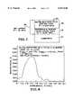
- FIG. 1schematically illustrates the athermal or non-thermal (buffer-layer) approach to stress reduction in accordance with the present invention.
- FIG. 2graphically illustrates that the Mo/Si multilayer film stress is a function of the Mo fraction in the multilayer.
- FIG. 3schematically illustrates a Mo/Si multilayer with an Mo/Si buffer-layer of a different Mo fraction.
- FIG. 4graphically illustrates reflectance measurements of an Mo/Si multilayer with an Mo/Si buffer layer, as in FIG. 3.
- FIG. 5schematically illustrates a preferred embodiment wherein the buffer-layer method of the present invention is applied to an Mo/Si multilayer using a Mo/Be buffer-layer on a silicon substrate.
- FIG. 6graphically illustrates reflectance measurements of a Mo/Si multilayer deposited on a Mo/Be buffer-layer, as in FIG. 5.
- FIG. 7schematically illustrates the non-thermal stress compensation technique of the present invention applied to a Mo/Be multilayer using an amorphous silicon buffer-layer.
- FIG. 8graphically illustrates reflectance measurements of an Mo/Be multilayer deposited on an amorphous silicon buffer-layer on a silicon substrate, as in FIG. 7.
- FIG. 9graphically illustrates reflectance measurements of a Mo/Be multilayer deposited on Si (100) substrate with and without a buffer-layer.
- the present inventionis directed to a method to reduce or negate multilayer film stress induced deformation of optics (substrates).
- the technique of the present inventioninvolves a buffer-layer intermediate the substrate and the multilayer.
- an optic (substrate)will deform when a stressed multilayer film is deposited upon it.
- Mo/Si and Mo/Be multilayer films with good reflectances>60%) have large film stresses (>400 and >330 MPa respectively).
- conventionally fabricated Mo/Si or Mo/Be multilayers deposited directly on substratesare not desirable candidates for use in a EUV lithography process which rely on optics using multilayer films to effectively reflect light in the 11-14 nm region, because the high stress of the multilayers alters the very accurate figure specifications.
- the present inventionprovides multilayer reflective films having high reflectance and low stress, thereby providing a viable multilayer for the several optics of a EUV lithography system.
- a buffer-layerintermediate the substrate (optic) and the reflective multilayer, the magnitude of the stress is reduced to under 100 MPa with minimal (near zero to 1.5%) loss in reflectance.
- Recent efforts utilizing the present inventionhave established that the magnitude of the stress of less than 30 MPa with a minimal loss of less than 1% in reflectance can be obtained.
- the buffer-layermust be very smooth (less than 0.3 nm rms roughness) and have a stress of sufficient magnitude and opposite in sign to cancel out or greatly reduce deformation in the optic (substrate) due to the stress in the multilayer.
- a stress of 400 MPafor example, can be reduced to less than 100 MPa, preferably to less than 30 MPa.
- This inventionenables a tunable, near-zero net film stress, or enables adjusting the stress, and hence results in little or no deformation of the optic (substrate).
- the technique of the present invention(the use of a buffer-layer) enables the net stress/curvature to be tuned to zero without the need to vary the processing conditions of the optimized, high reflectance multilayer.
- this inventiondoes not require that any of the films (or layers) be epitaxial, or even crystalline, and thus the film growth can be done at any temperature (including ambient).
- Mo/Si and Mo/Be multilayersWhile the following examples utilize Mo/Si and Mo/Be multilayers, other molybdenum containing materials may be utilized for the multilayers, such as Mo/Y, Mo 2 C/Si, Mo 2 C/Be, Mo/C, and Mo/Sr. Also, Mo 2 C/Si, Mo 2 C/Be, and a-C, or other material which is opposite in stress to the multilayer stress and is very smooth, can be used as the buffer layer.
- FIG. 1schematically illustrates the invention, wherein a reflective device indicated at 10 comprises a substrate (optic) 11, a buffer-layer 12, and a multilayer film 13.
- the substrate 11may be composed of silicon, low thermal expansion glass, ceramics such as Zerodur or ULE or Zerodur M, quartz, float glass, and sapphire.
- the buffer-layer 12, as shown,has a positive stress while the multilayer film 13 has a negative stress, depending on the application, such that the net film stress is zero, as indicated at 14.
- the positive stress in the buffer-layer 12equals the negative stress in the multilayer film 13, but the stresses need not be equal, but preferably near equal, and such can be tuned, for example, by the composition of the buffer-layer 12, as discussed in greater detail hereinafter.
- the stress thereofmay be positive and thus the stress in the buffer-layer 12 must be designed to be negative, to provide the desired near-zero net film stress.
- the buffer-layer approach to stress reductionprovides the potential to tailor the net film stress (curvature) to any desired level.
- the buffer-layermay be a multilayer, a composite, or a single layer depending on the compositions of the multilayer film and the buffer-layer.
- FIG. 2illustrates that the multilayer film stress is a function of the Mo fraction (Mo to Si ratio) in an Mo/Si multilayer film, wherein the constant () equals 6.9-7.0 nm.
- the stress of the Mo/Si multilayer filmcan be tuned by adjusting the Mo fraction.
- the graph of FIG. 2illustrates a non-linear behavior as a result of increasing the Mo fraction.
- FIG. 3schematically illustrates a simples method for reducing, tuning, or adjusting stress in a Mo/Si multilayer in accordance with the invention, which involves employing a Mo/Si buffer-layer.
- the device 20comprises a substrate (optic) 21, which may be silicon, a buffer-layer 22 of Mo/Si, and a multilayer film 23 of Mo/Si.
- the multilayer film 23is composed of 40 bi-layers having a Mo fraction ( ⁇ ) of 0.4, and a stress of -420 MPa.
- FIG. 4graphically illustrates the reflectance measurements of a Mo/Si multilayer film with a Mo fraction of 0.4 (40%), with a Mo/Si buffer-layer with a Mo fraction of 0.8 (80%), on a silicon (Si) substrate.
- the peak reflectance (R peak)equaled 62.8%, at a wavelength of 113.35 nm measured at 5° from normal incidence, results in a net multilayer (ML) stress equal to -70 MPa and a 3-4% loss in reflectance compared to that of the non-buffered Mo/Si multilayer.
- FIG. 5schematically illustrates a preferred embodiment of the invention with the reflective multilayer film composed of Mo/Si and the buffer-layer composed of Mo/Be, on a Si (100) substrate.
- the device indicated at 30has a substrate 31 of Si 100, a Mo/Be buffer-layer 32 having a thickness of 300 nm, and a Mo/Si multilayer film 33 having a thickness of 280 nm, which produced a net stress indicated at 34 equal to -28 MPa, with ⁇ 1% reduction in reflectance compared to a non-buffered multilayer coating.
- the buffer-layer technique of this inventioncan be successfully applied to the Mo/Si system by using a Mo/Be buffer-layer.
- the thickness of the Mo/Be buffer layer(or individual layers) can be tailored to reduce or negate the stress of the Mo/Si multilayer film with minimal reflectance loss.
- a Mo/Be buffer layer with 53 bi-layers and a bi-layer thickness of approximately 5.8 nmwas deposited on a silicon (100) substrate, and then a 40 bi-layer, high reflectance Mo/Si film with a bi-layer thickness of 6.9 nm was deposited upon the Mo/Be buffer-layer.
- the net stress of the combined filmswas only -28 MPa, and yielded a peak reflectance of 66.5% at a wavelength of 13.33 nm (5° from normal incidence), as shown in FIG. 6.
- FIG. 7schematically illustrates an embodiment of a non-thermal stress compensation technique in accordance with the present invention that has been successfully demonstrated for a Mo/Be multilayer system. It has not been demonstrated that this technique can be used to reduce or negate the multilayer film stress induced deformation of substrates (optics) for Mo/Be multilayer films as well as Mo/Si multilayer films.
- the embodiment of FIG. 8comprises a device generally indicated at 40 composed of a substrate 41, a buffer layer 42, and a Mo/Be multilayer film 43.
- the buffer-layer 42was formed of amorphous silicon deposited at room temperature by making 33 passes of the silicon substrate 41 over a silicon sputtering target.
- the total amorphous silicon (a-Si) film thicknesswas 110 nm, and the film stress was approximately -1300 MPa (compressive). Then a 400 nm Mo/Be multilayer film 43 was deposited upon the a-Si buffer layer film 42, and the net film stress, indicated at 44, was a low -22 MPa (compressive). During the same deposition run, another Mo/Be multilayer was deposited (under identical conditions) on a silicon substrate with no a-Si buffer-layer, and the film stress was rather high, 3332 MPa (tensile).
- FIG. 9illustrates multilayers of Mo/Be with and without a buffer-layer, which were deposited during the same experimental or deposition run.
- Mo/Be multilayerswere deposited on an Si (100) substrate, and having an Rmax of 69.4% and a stress of +333 MPa.
- Mo/Be multilayerswere deposited on an a-Si buffer-layer deposited on an Si (100) substrate, which resulted in an Rmax of 68.7% and a stress of -22 MPa.
- the buffer-layerthe stress was reduced from +333 MPa to -22 MPa, with only a 0.7% reduction or loss in reflectance.
- the present inventionis applicable to crystalline and non-crystalline materials, and can be used at ambient temperatures. Also, the invention enables adjusting the stress by increasing the thickness of the buffer layer, provided it is not increased to a point where reflectance loss results.
- the present inventionprovides a non-thermal buffer-layer technique that can be used to reduce the multilayer film stress-induced curvature of substrates (optics) to near zero levels while still maintaining a high reflectivity in the extreme ultraviolet (EUV) wavelength region.
- the composition, thickness, etc. of the buffer-layerscan be turned to negate the stress in the multilayer film. While the description has been directed to Mo/Si and Mo/Be multilayer films, the buffer-layer approach can be successfully utilized to reduce stress in other multilayer systems.
- While the inventionprovides reduced stress multilayer films which have particular application in EUV lithography system, such can have significant impact on miniaturization of electronic devices, as well as being useful in any application requiring high reflectance-low stress optical coating, such as in the soft x-ray and EUV wavelength regions for applications in x-ray research, x-ray spectroscopy, x-ray microscopy, x-ray astronomy, and synchrotron optics.
Landscapes
- Physics & Mathematics (AREA)
- General Physics & Mathematics (AREA)
- Optics & Photonics (AREA)
- Health & Medical Sciences (AREA)
- Engineering & Computer Science (AREA)
- Environmental & Geological Engineering (AREA)
- Epidemiology (AREA)
- Public Health (AREA)
- Exposure Of Semiconductors, Excluding Electron Or Ion Beam Exposure (AREA)
- Exposure And Positioning Against Photoresist Photosensitive Materials (AREA)
- Optical Elements Other Than Lenses (AREA)
Abstract
Description
Claims (27)
Priority Applications (6)
| Application Number | Priority Date | Filing Date | Title |
|---|---|---|---|
| US09/027,309US6011646A (en) | 1998-02-20 | 1998-02-20 | Method to adjust multilayer film stress induced deformation of optics |
| JP2000532776AJP2002504715A (en) | 1998-02-20 | 1999-02-17 | Method for controlling deformation of optical element caused by stress in multilayer film |
| PCT/US1999/003411WO1999042901A1 (en) | 1998-02-20 | 1999-02-17 | Method to adjust multilayer film stress induced deformation of optics |
| AU32978/99AAU3297899A (en) | 1998-02-20 | 1999-02-17 | Method to adjust multilayer film stress induced deformation of optics |
| EP99934346AEP1057077A1 (en) | 1998-02-20 | 1999-02-17 | Method to adjust multilayer film stress induced deformation of optics |
| KR1020007009123AKR20010041084A (en) | 1998-02-20 | 1999-02-17 | Mathod to adjust multilayer film stress induced deformation of optics |
Applications Claiming Priority (1)
| Application Number | Priority Date | Filing Date | Title |
|---|---|---|---|
| US09/027,309US6011646A (en) | 1998-02-20 | 1998-02-20 | Method to adjust multilayer film stress induced deformation of optics |
Publications (1)
| Publication Number | Publication Date |
|---|---|
| US6011646Atrue US6011646A (en) | 2000-01-04 |
Family
ID=21836941
Family Applications (1)
| Application Number | Title | Priority Date | Filing Date |
|---|---|---|---|
| US09/027,309Expired - LifetimeUS6011646A (en) | 1998-02-20 | 1998-02-20 | Method to adjust multilayer film stress induced deformation of optics |
Country Status (6)
| Country | Link |
|---|---|
| US (1) | US6011646A (en) |
| EP (1) | EP1057077A1 (en) |
| JP (1) | JP2002504715A (en) |
| KR (1) | KR20010041084A (en) |
| AU (1) | AU3297899A (en) |
| WO (1) | WO1999042901A1 (en) |
Cited By (70)
| Publication number | Priority date | Publication date | Assignee | Title |
|---|---|---|---|---|
| DE10011548A1 (en)* | 2000-02-28 | 2001-09-06 | Fraunhofer Ges Forschung | Thermally stable layer system used for reflecting extreme UV rays consists of layer pairs made up of a barrier layer of molybdenum silicide between a molybdenum layer and a silicon layer |
| DE10011547A1 (en)* | 2000-02-28 | 2001-09-06 | Fraunhofer Ges Forschung | Thermally stable layer system used for reflecting extreme UV rays consists of layer pairs made up of a barrier layer of molybdenum carbide between molybdenum layer and a silicon layer |
| US6309705B1 (en)* | 1998-02-20 | 2001-10-30 | The Regents Of The University Of California | Process for fabricating high reflectance-low stress Mo—Si multilayer reflective coatings |
| US6392775B1 (en)* | 1998-01-13 | 2002-05-21 | Seagate Technology Llc | Optical reflector for micro-machined mirrors |
| US20020167070A1 (en)* | 2000-06-30 | 2002-11-14 | Motorola, Inc. | Hybrid semiconductor structure and device |
| US6493497B1 (en) | 2000-09-26 | 2002-12-10 | Motorola, Inc. | Electro-optic structure and process for fabricating same |
| US6501121B1 (en) | 2000-11-15 | 2002-12-31 | Motorola, Inc. | Semiconductor structure |
| US20030022430A1 (en)* | 2001-07-24 | 2003-01-30 | Motorola, Inc. | Structure and method for fabricating configurable transistor devices utilizing the formation of a compliant substrate for materials used to form the same |
| US20030036217A1 (en)* | 2001-08-16 | 2003-02-20 | Motorola, Inc. | Microcavity semiconductor laser coupled to a waveguide |
| US6531740B2 (en) | 2001-07-17 | 2003-03-11 | Motorola, Inc. | Integrated impedance matching and stability network |
| US6555946B1 (en) | 2000-07-24 | 2003-04-29 | Motorola, Inc. | Acoustic wave device and process for forming the same |
| US6559471B2 (en) | 2000-12-08 | 2003-05-06 | Motorola, Inc. | Quantum well infrared photodetector and method for fabricating same |
| US6590236B1 (en) | 2000-07-24 | 2003-07-08 | Motorola, Inc. | Semiconductor structure for use with high-frequency signals |
| US6589856B2 (en) | 2001-08-06 | 2003-07-08 | Motorola, Inc. | Method and apparatus for controlling anti-phase domains in semiconductor structures and devices |
| US6617082B2 (en)* | 2001-06-29 | 2003-09-09 | Intel Corporation | Microelectromechanical system mask |
| US6639249B2 (en) | 2001-08-06 | 2003-10-28 | Motorola, Inc. | Structure and method for fabrication for a solid-state lighting device |
| US6638838B1 (en) | 2000-10-02 | 2003-10-28 | Motorola, Inc. | Semiconductor structure including a partially annealed layer and method of forming the same |
| US20030207589A1 (en)* | 2002-05-03 | 2003-11-06 | Thoughtbeam, Inc. | Method for growing a monocrystalline oxide layer and for fabricating a semiconductor device on a monocrystalline substrate |
| US6646293B2 (en) | 2001-07-18 | 2003-11-11 | Motorola, Inc. | Structure for fabricating high electron mobility transistors utilizing the formation of complaint substrates |
| US6667196B2 (en) | 2001-07-25 | 2003-12-23 | Motorola, Inc. | Method for real-time monitoring and controlling perovskite oxide film growth and semiconductor structure formed using the method |
| US6673646B2 (en) | 2001-02-28 | 2004-01-06 | Motorola, Inc. | Growth of compound semiconductor structures on patterned oxide films and process for fabricating same |
| US6673667B2 (en) | 2001-08-15 | 2004-01-06 | Motorola, Inc. | Method for manufacturing a substantially integral monolithic apparatus including a plurality of semiconductor materials |
| US20040012037A1 (en)* | 2002-07-18 | 2004-01-22 | Motorola, Inc. | Hetero-integration of semiconductor materials on silicon |
| US6693033B2 (en) | 2000-02-10 | 2004-02-17 | Motorola, Inc. | Method of removing an amorphous oxide from a monocrystalline surface |
| US6693298B2 (en) | 2001-07-20 | 2004-02-17 | Motorola, Inc. | Structure and method for fabricating epitaxial semiconductor on insulator (SOI) structures and devices utilizing the formation of a compliant substrate for materials used to form same |
| US6709989B2 (en) | 2001-06-21 | 2004-03-23 | Motorola, Inc. | Method for fabricating a semiconductor structure including a metal oxide interface with silicon |
| US20040069991A1 (en)* | 2002-10-10 | 2004-04-15 | Motorola, Inc. | Perovskite cuprate electronic device structure and process |
| US20040070312A1 (en)* | 2002-10-10 | 2004-04-15 | Motorola, Inc. | Integrated circuit and process for fabricating the same |
| US20040100638A1 (en)* | 2002-11-27 | 2004-05-27 | The Regents Of The University Of California. | Correcting surface contour of a non-rigid object through control of surface residual stress |
| US20040150043A1 (en)* | 2003-02-03 | 2004-08-05 | Motorola, Inc. | Structure and method for fabricating semiconductor microresonator devices |
| US20040151463A1 (en)* | 2003-02-03 | 2004-08-05 | Motorola, Inc. | Optical waveguide structure and method for fabricating the same |
| US20040149202A1 (en)* | 2000-02-10 | 2004-08-05 | Motorola, Inc. | Semiconductor structure, semiconductor device, communicating device, integrated circuit, and process for fabricating the same |
| US6780496B2 (en)* | 2001-07-03 | 2004-08-24 | Euv Llc | Optimized capping layers for EUV multilayers |
| US20040164315A1 (en)* | 2003-02-25 | 2004-08-26 | Motorola, Inc. | Structure and device including a tunneling piezoelectric switch and method of forming same |
| US20040217444A1 (en)* | 2001-10-17 | 2004-11-04 | Motorola, Inc. | Method and apparatus utilizing monocrystalline insulator |
| US20040232431A1 (en)* | 2001-07-16 | 2004-11-25 | Motorola, Inc. | Semiconductor structure and method for implementing cross-point switch functionality |
| US6835503B2 (en) | 2002-04-12 | 2004-12-28 | Micron Technology, Inc. | Use of a planarizing layer to improve multilayer performance in extreme ultra-violet masks |
| US20050023622A1 (en)* | 2000-05-31 | 2005-02-03 | Motorola | Semiconductor device and method |
| US20050056210A1 (en)* | 2000-07-24 | 2005-03-17 | Motorola | Heterojunction tunneling diodes and process for fabricating same |
| EP1333298A3 (en)* | 2002-01-25 | 2005-04-13 | Alps Electric Co., Ltd. | Multilayer film optical filter, method of producing the same, and optical component using the same |
| US6885065B2 (en) | 2002-11-20 | 2005-04-26 | Freescale Semiconductor, Inc. | Ferromagnetic semiconductor structure and method for forming the same |
| US20050194593A1 (en)* | 2001-01-19 | 2005-09-08 | Freescale Semiconductor, Inc. | Structure and method for fabricating GaN devices utilizing the formation of a compliant substrate |
| US20050213198A1 (en)* | 2004-03-29 | 2005-09-29 | Lee Sang H | Broad-angle multilayer mirror design |
| US6992321B2 (en) | 2001-07-13 | 2006-01-31 | Motorola, Inc. | Structure and method for fabricating semiconductor structures and devices utilizing piezoelectric materials |
| US20060062348A1 (en)* | 2003-06-02 | 2006-03-23 | Nikon Corporation | Multilayer film reflector and X-ray exposure system |
| US7019332B2 (en) | 2001-07-20 | 2006-03-28 | Freescale Semiconductor, Inc. | Fabrication of a wavelength locker within a semiconductor structure |
| US7045815B2 (en) | 2001-04-02 | 2006-05-16 | Freescale Semiconductor, Inc. | Semiconductor structure exhibiting reduced leakage current and method of fabricating same |
| US7161227B2 (en) | 2001-08-14 | 2007-01-09 | Motorola, Inc. | Structure and method for fabricating semiconductor structures and devices for detecting an object |
| US7169619B2 (en) | 2002-11-19 | 2007-01-30 | Freescale Semiconductor, Inc. | Method for fabricating semiconductor structures on vicinal substrates using a low temperature, low pressure, alkaline earth metal-rich process |
| US20070188870A1 (en)* | 2005-10-11 | 2007-08-16 | Akira Miyake | Multilayer mirror manufacturing method, optical system manufacturing method, exposure apparatus, and device manufacturing method |
| CN100394214C (en)* | 2002-11-21 | 2008-06-11 | 台达电子工业股份有限公司 | Film stress balance coating method and optical assembly manufactured by using same |
| US20080153010A1 (en)* | 2006-11-09 | 2008-06-26 | Asahi Glass Company., Ltd. | Method for depositing reflective multilayer film of reflective mask blank for euv lithography and method for producing reflective mask blank for euv lithography |
| EP2068325A1 (en)* | 2007-12-05 | 2009-06-10 | Canon Kabushiki Kaisha | Optical element for X-ray |
| US20090252977A1 (en)* | 2008-04-07 | 2009-10-08 | Canon Kabushiki Kaisha | Multilayer film reflector |
| DE102008042212A1 (en)* | 2008-09-19 | 2010-04-01 | Carl Zeiss Smt Ag | Reflective optical element and method for its production |
| EP2174170A1 (en)* | 2007-07-27 | 2010-04-14 | SELEX Galileo S.p.A. | Preliminary controlled pre-deformation treatment for the production of mirrors |
| US20110222144A1 (en)* | 2008-06-12 | 2011-09-15 | Carl Zeiss Smt Gmbh | Method for producing a multilayer coating, optical element and optical arrangement |
| DE102011080052A1 (en) | 2011-07-28 | 2013-01-31 | Carl Zeiss Smt Gmbh | Mirror, optical system with mirror and method for producing a mirror |
| US8928972B2 (en) | 2009-12-15 | 2015-01-06 | Carl Zeiss Smt Gmbh | Reflective optical element for EUV lithography |
| TWI474056B (en)* | 2009-07-10 | 2015-02-21 | Zeiss Carl Smt Gmbh | Mirror for the euv wavelength range, projection objective for microlithography comprising such a mirror, and projection exposure apparatus for microlithography comprising such a projection objective |
| WO2015114043A1 (en) | 2014-01-30 | 2015-08-06 | Carl Zeiss Smt Gmbh | Method for producing a mirror element |
| DE102014219648A1 (en) | 2014-09-29 | 2015-10-15 | Carl Zeiss Smt Gmbh | Method for producing a mirror element |
| US9261773B2 (en) | 2013-02-20 | 2016-02-16 | Asahi Glass Company, Limited | Reflective mask blank for EUV lithography, and reflective layer-coated substrate for EUV lithography |
| US9423684B2 (en) | 2011-11-25 | 2016-08-23 | Asahi Glass Company, Limited | Reflective mask blank for EUV lithography and process for its production |
| US20160357038A1 (en)* | 2014-12-05 | 2016-12-08 | Boe Technology Group Co., Ltd. | Curved Liquid Crystal Display Panel and Curved Liquid Crystal Display Device |
| US9651723B2 (en) | 2012-10-26 | 2017-05-16 | Kyocera Corporation | Optical filter member and imaging device provided with the same |
| US9804309B1 (en)* | 2014-04-22 | 2017-10-31 | Kla-Tencor Corporation | Reducing extrinsic stress in thin film optical mirrors and filters for deep ultraviolet |
| US10879177B2 (en)* | 2015-06-19 | 2020-12-29 | Applied Materials, Inc. | PVD deposition and anneal of multi-layer metal-dielectric film |
| US11385383B2 (en) | 2018-11-13 | 2022-07-12 | Raytheon Company | Coating stress mitigation through front surface coating manipulation on ultra-high reflectors or other optical devices |
| WO2025087653A1 (en)* | 2023-10-24 | 2025-05-01 | Carl Zeiss Smt Gmbh | Optical element and euv lithography system |
Families Citing this family (16)
| Publication number | Priority date | Publication date | Assignee | Title |
|---|---|---|---|---|
| US6134049A (en)* | 1998-09-25 | 2000-10-17 | The Regents Of The University Of California | Method to adjust multilayer film stress induced deformation of optics |
| CA2416289C (en)* | 2000-07-21 | 2012-12-04 | Essentia Biosystems, Inc. | Multi-component biological transport systems |
| KR100588126B1 (en)* | 2001-12-04 | 2006-06-09 | 에이에스엠엘 네델란즈 비.브이. | Lithographic apparatus, device manufacturing method and optical element manufacturing method |
| JP4917156B2 (en)* | 2002-03-29 | 2012-04-18 | Hoya株式会社 | Mask blank manufacturing method and transfer mask manufacturing method |
| FR2853418B1 (en)* | 2003-04-01 | 2005-08-19 | Commissariat Energie Atomique | OPTICAL DEVICE WITH REINFORCED MECHANICAL STABILITY OPERATING IN THE EXTREME ULTRAVIOLET AND LITHOGRAPHY MASK COMPRISING SUCH A DEVICE |
| BRPI0508440A (en) | 2004-03-03 | 2007-07-24 | Revance Therapeutics Inc | compositions and methods for topical diagnosis and therapeutic transport |
| US9211248B2 (en) | 2004-03-03 | 2015-12-15 | Revance Therapeutics, Inc. | Compositions and methods for topical application and transdermal delivery of botulinum toxins |
| RU2007136616A (en) | 2005-03-03 | 2009-04-10 | Риванс Терапьютикс, Инк. (Us) | COMPOSITION AND METHOD FOR LOCAL USE AND PERFORMANCE OF BOTULIN TOXIN |
| JP2008109060A (en)* | 2005-11-10 | 2008-05-08 | Asahi Glass Co Ltd | Method for forming a multilayer reflective film of a reflective mask blank for EUV lithography, and method for manufacturing a reflective mask blank for EUV lithography |
| JP2007329368A (en)* | 2006-06-09 | 2007-12-20 | Canon Inc | Multilayer mirror, evaluation method, exposure apparatus and device manufacturing method |
| EP2087510A4 (en)* | 2006-11-27 | 2010-05-05 | Nikon Corp | Optical element, exposure unit utilizing the same and process for device production |
| JP5362969B2 (en)* | 2007-08-21 | 2013-12-11 | リコー光学株式会社 | Optical element |
| DE102011079933A1 (en)* | 2010-08-19 | 2012-02-23 | Carl Zeiss Smt Gmbh | Optical element for UV or EUV lithography |
| JP2012068125A (en)* | 2010-09-24 | 2012-04-05 | Canon Inc | X-ray waveguide |
| JP2013122952A (en)* | 2011-12-09 | 2013-06-20 | Asahi Glass Co Ltd | Reflection-type mask blank for euv lithography, manufacturing method thereof, and manufacturing method of substrate with reflection layer for mask blank |
| JP2015018918A (en)* | 2013-07-10 | 2015-01-29 | キヤノン株式会社 | Reflective master, exposure method and device manufacturing method |
Citations (2)
| Publication number | Priority date | Publication date | Assignee | Title |
|---|---|---|---|---|
| US5433988A (en)* | 1986-10-01 | 1995-07-18 | Canon Kabushiki Kaisha | Multi-layer reflection mirror for soft X-ray to vacuum ultraviolet ray |
| US5841584A (en)* | 1995-04-26 | 1998-11-24 | Sharp Kabushiki Kaisha | Dielectric multilayered reflector |
Family Cites Families (3)
| Publication number | Priority date | Publication date | Assignee | Title |
|---|---|---|---|---|
| JPS6437014A (en)* | 1987-07-31 | 1989-02-07 | Sharp Kk | Mask for x-ray lithography |
| FR2675948A1 (en)* | 1991-04-23 | 1992-10-30 | Centre Nat Rech Scient | SEMICONDUCTOR MATERIALS WITH HETEROEPITAXIC STRUCTURE AND CONTROLLED STRESS, THEIR METHOD OF PRODUCTION AND THEIR APPLICATIONS. |
| US5500312A (en)* | 1994-10-11 | 1996-03-19 | At&T Corp. | Masks with low stress multilayer films and a process for controlling the stress of multilayer films |
- 1998
- 1998-02-20USUS09/027,309patent/US6011646A/ennot_activeExpired - Lifetime
- 1999
- 1999-02-17EPEP99934346Apatent/EP1057077A1/ennot_activeWithdrawn
- 1999-02-17AUAU32978/99Apatent/AU3297899A/ennot_activeAbandoned
- 1999-02-17JPJP2000532776Apatent/JP2002504715A/enactivePending
- 1999-02-17KRKR1020007009123Apatent/KR20010041084A/ennot_activeWithdrawn
- 1999-02-17WOPCT/US1999/003411patent/WO1999042901A1/ennot_activeApplication Discontinuation
Patent Citations (2)
| Publication number | Priority date | Publication date | Assignee | Title |
|---|---|---|---|---|
| US5433988A (en)* | 1986-10-01 | 1995-07-18 | Canon Kabushiki Kaisha | Multi-layer reflection mirror for soft X-ray to vacuum ultraviolet ray |
| US5841584A (en)* | 1995-04-26 | 1998-11-24 | Sharp Kabushiki Kaisha | Dielectric multilayered reflector |
Non-Patent Citations (10)
| Title |
|---|
| Kassner et al, J. Mat. Sci. 31, 2291 (1996).* |
| Kola et al, Appl. Phys. Lett. 60,3120 (1992).* |
| Nguyen et al, (Optical Society of America, Washington, D.C., 1994), vol. 23, p. 56.* |
| Nguyen et al, Physics of X Ray Multilayer Structures (Optical Society of America, Wash. D.C. 1994), vol. 6, p. 102.* |
| Nguyen et al, Physics of X-Ray Multilayer Structures (Optical Society of America, Wash. D.C. 1994), vol. 6, p. 102. |
| Rosen et al, Nanostruc. Mater. 3, 195 (1993).* |
| Skulina et al, Appl. Optics 34, 3727 (1995).* |
| Stearns et al, Mater. Res. Soc. Symp. Proc., vol. 382, p. 329 (MRS, 1995).* |
| Tinone et al, J. Electron Spectrosc. Relat. Phenom. 80, 461 (1996).* |
| Windt et al, J. Appl. Phys. 78, 2423 (1995).* |
Cited By (102)
| Publication number | Priority date | Publication date | Assignee | Title |
|---|---|---|---|---|
| US6392775B1 (en)* | 1998-01-13 | 2002-05-21 | Seagate Technology Llc | Optical reflector for micro-machined mirrors |
| US6309705B1 (en)* | 1998-02-20 | 2001-10-30 | The Regents Of The University Of California | Process for fabricating high reflectance-low stress Mo—Si multilayer reflective coatings |
| GB2368070B (en)* | 1999-03-08 | 2003-10-22 | Seagate Technology Llc | Improved optical reflector for micro-machined mirrors |
| US20040232525A1 (en)* | 2000-02-10 | 2004-11-25 | Motorola, Inc. | Semiconductor structure, semiconductor device, communicating device, integrated circuit, and process for fabricating the same |
| US20040150076A1 (en)* | 2000-02-10 | 2004-08-05 | Motorola, Inc. | Semiconductor structure, semiconductor device, communicating device, integrated circuit, and process for fabricating the same |
| US20040150003A1 (en)* | 2000-02-10 | 2004-08-05 | Motorola, Inc. | Semiconductor structure, semiconductor device, communicating device, integrated circuit, and process for fabricating the same |
| US20040149202A1 (en)* | 2000-02-10 | 2004-08-05 | Motorola, Inc. | Semiconductor structure, semiconductor device, communicating device, integrated circuit, and process for fabricating the same |
| US7067856B2 (en) | 2000-02-10 | 2006-06-27 | Freescale Semiconductor, Inc. | Semiconductor structure, semiconductor device, communicating device, integrated circuit, and process for fabricating the same |
| US6693033B2 (en) | 2000-02-10 | 2004-02-17 | Motorola, Inc. | Method of removing an amorphous oxide from a monocrystalline surface |
| DE10011548C2 (en)* | 2000-02-28 | 2003-06-18 | Fraunhofer Ges Forschung | Process for producing a thermally stable layer system for reflecting radiation in the extreme ultraviolet spectral range (EUV) |
| DE10011548A1 (en)* | 2000-02-28 | 2001-09-06 | Fraunhofer Ges Forschung | Thermally stable layer system used for reflecting extreme UV rays consists of layer pairs made up of a barrier layer of molybdenum silicide between a molybdenum layer and a silicon layer |
| DE10011547A1 (en)* | 2000-02-28 | 2001-09-06 | Fraunhofer Ges Forschung | Thermally stable layer system used for reflecting extreme UV rays consists of layer pairs made up of a barrier layer of molybdenum carbide between molybdenum layer and a silicon layer |
| DE10011547C2 (en)* | 2000-02-28 | 2003-06-12 | Fraunhofer Ges Forschung | Thermally stable layer system for reflection of radiation in the extreme ultraviolet spectral range (EUV) |
| US20050023622A1 (en)* | 2000-05-31 | 2005-02-03 | Motorola | Semiconductor device and method |
| US7005717B2 (en) | 2000-05-31 | 2006-02-28 | Freescale Semiconductor, Inc. | Semiconductor device and method |
| US20020167070A1 (en)* | 2000-06-30 | 2002-11-14 | Motorola, Inc. | Hybrid semiconductor structure and device |
| US6590236B1 (en) | 2000-07-24 | 2003-07-08 | Motorola, Inc. | Semiconductor structure for use with high-frequency signals |
| US7105866B2 (en) | 2000-07-24 | 2006-09-12 | Freescale Semiconductor, Inc. | Heterojunction tunneling diodes and process for fabricating same |
| US6555946B1 (en) | 2000-07-24 | 2003-04-29 | Motorola, Inc. | Acoustic wave device and process for forming the same |
| US20050056210A1 (en)* | 2000-07-24 | 2005-03-17 | Motorola | Heterojunction tunneling diodes and process for fabricating same |
| US6493497B1 (en) | 2000-09-26 | 2002-12-10 | Motorola, Inc. | Electro-optic structure and process for fabricating same |
| US6638838B1 (en) | 2000-10-02 | 2003-10-28 | Motorola, Inc. | Semiconductor structure including a partially annealed layer and method of forming the same |
| US6501121B1 (en) | 2000-11-15 | 2002-12-31 | Motorola, Inc. | Semiconductor structure |
| US6559471B2 (en) | 2000-12-08 | 2003-05-06 | Motorola, Inc. | Quantum well infrared photodetector and method for fabricating same |
| US20050194593A1 (en)* | 2001-01-19 | 2005-09-08 | Freescale Semiconductor, Inc. | Structure and method for fabricating GaN devices utilizing the formation of a compliant substrate |
| US7211852B2 (en) | 2001-01-19 | 2007-05-01 | Freescale Semiconductor, Inc. | Structure and method for fabricating GaN devices utilizing the formation of a compliant substrate |
| US6673646B2 (en) | 2001-02-28 | 2004-01-06 | Motorola, Inc. | Growth of compound semiconductor structures on patterned oxide films and process for fabricating same |
| US7045815B2 (en) | 2001-04-02 | 2006-05-16 | Freescale Semiconductor, Inc. | Semiconductor structure exhibiting reduced leakage current and method of fabricating same |
| US6709989B2 (en) | 2001-06-21 | 2004-03-23 | Motorola, Inc. | Method for fabricating a semiconductor structure including a metal oxide interface with silicon |
| US6617082B2 (en)* | 2001-06-29 | 2003-09-09 | Intel Corporation | Microelectromechanical system mask |
| US6780496B2 (en)* | 2001-07-03 | 2004-08-24 | Euv Llc | Optimized capping layers for EUV multilayers |
| US6992321B2 (en) | 2001-07-13 | 2006-01-31 | Motorola, Inc. | Structure and method for fabricating semiconductor structures and devices utilizing piezoelectric materials |
| US20040232431A1 (en)* | 2001-07-16 | 2004-11-25 | Motorola, Inc. | Semiconductor structure and method for implementing cross-point switch functionality |
| US6531740B2 (en) | 2001-07-17 | 2003-03-11 | Motorola, Inc. | Integrated impedance matching and stability network |
| US6646293B2 (en) | 2001-07-18 | 2003-11-11 | Motorola, Inc. | Structure for fabricating high electron mobility transistors utilizing the formation of complaint substrates |
| US6693298B2 (en) | 2001-07-20 | 2004-02-17 | Motorola, Inc. | Structure and method for fabricating epitaxial semiconductor on insulator (SOI) structures and devices utilizing the formation of a compliant substrate for materials used to form same |
| US7019332B2 (en) | 2001-07-20 | 2006-03-28 | Freescale Semiconductor, Inc. | Fabrication of a wavelength locker within a semiconductor structure |
| US20030022430A1 (en)* | 2001-07-24 | 2003-01-30 | Motorola, Inc. | Structure and method for fabricating configurable transistor devices utilizing the formation of a compliant substrate for materials used to form the same |
| US6855992B2 (en) | 2001-07-24 | 2005-02-15 | Motorola Inc. | Structure and method for fabricating configurable transistor devices utilizing the formation of a compliant substrate for materials used to form the same |
| US6667196B2 (en) | 2001-07-25 | 2003-12-23 | Motorola, Inc. | Method for real-time monitoring and controlling perovskite oxide film growth and semiconductor structure formed using the method |
| US6589856B2 (en) | 2001-08-06 | 2003-07-08 | Motorola, Inc. | Method and apparatus for controlling anti-phase domains in semiconductor structures and devices |
| US6639249B2 (en) | 2001-08-06 | 2003-10-28 | Motorola, Inc. | Structure and method for fabrication for a solid-state lighting device |
| US7161227B2 (en) | 2001-08-14 | 2007-01-09 | Motorola, Inc. | Structure and method for fabricating semiconductor structures and devices for detecting an object |
| US6673667B2 (en) | 2001-08-15 | 2004-01-06 | Motorola, Inc. | Method for manufacturing a substantially integral monolithic apparatus including a plurality of semiconductor materials |
| US20030036217A1 (en)* | 2001-08-16 | 2003-02-20 | Motorola, Inc. | Microcavity semiconductor laser coupled to a waveguide |
| US20040217444A1 (en)* | 2001-10-17 | 2004-11-04 | Motorola, Inc. | Method and apparatus utilizing monocrystalline insulator |
| US7342276B2 (en) | 2001-10-17 | 2008-03-11 | Freescale Semiconductor, Inc. | Method and apparatus utilizing monocrystalline insulator |
| EP1333298A3 (en)* | 2002-01-25 | 2005-04-13 | Alps Electric Co., Ltd. | Multilayer film optical filter, method of producing the same, and optical component using the same |
| US6835503B2 (en) | 2002-04-12 | 2004-12-28 | Micron Technology, Inc. | Use of a planarizing layer to improve multilayer performance in extreme ultra-violet masks |
| US20050084773A1 (en)* | 2002-04-12 | 2005-04-21 | Krauth Anthony C. | Use of a planarizing layer to improve multilayer performance in extreme ultraviolet masks |
| US7387853B2 (en) | 2002-04-12 | 2008-06-17 | Micron Technology, Inc. | Use of a planarizing layer to improve multilayer performance in ultraviolet masks |
| US6916717B2 (en) | 2002-05-03 | 2005-07-12 | Motorola, Inc. | Method for growing a monocrystalline oxide layer and for fabricating a semiconductor device on a monocrystalline substrate |
| US20030207589A1 (en)* | 2002-05-03 | 2003-11-06 | Thoughtbeam, Inc. | Method for growing a monocrystalline oxide layer and for fabricating a semiconductor device on a monocrystalline substrate |
| US20040012037A1 (en)* | 2002-07-18 | 2004-01-22 | Motorola, Inc. | Hetero-integration of semiconductor materials on silicon |
| US20040070312A1 (en)* | 2002-10-10 | 2004-04-15 | Motorola, Inc. | Integrated circuit and process for fabricating the same |
| US20040069991A1 (en)* | 2002-10-10 | 2004-04-15 | Motorola, Inc. | Perovskite cuprate electronic device structure and process |
| US7169619B2 (en) | 2002-11-19 | 2007-01-30 | Freescale Semiconductor, Inc. | Method for fabricating semiconductor structures on vicinal substrates using a low temperature, low pressure, alkaline earth metal-rich process |
| US6885065B2 (en) | 2002-11-20 | 2005-04-26 | Freescale Semiconductor, Inc. | Ferromagnetic semiconductor structure and method for forming the same |
| CN100394214C (en)* | 2002-11-21 | 2008-06-11 | 台达电子工业股份有限公司 | Film stress balance coating method and optical assembly manufactured by using same |
| US20040100638A1 (en)* | 2002-11-27 | 2004-05-27 | The Regents Of The University Of California. | Correcting surface contour of a non-rigid object through control of surface residual stress |
| US6965128B2 (en) | 2003-02-03 | 2005-11-15 | Freescale Semiconductor, Inc. | Structure and method for fabricating semiconductor microresonator devices |
| US20040151463A1 (en)* | 2003-02-03 | 2004-08-05 | Motorola, Inc. | Optical waveguide structure and method for fabricating the same |
| US7020374B2 (en) | 2003-02-03 | 2006-03-28 | Freescale Semiconductor, Inc. | Optical waveguide structure and method for fabricating the same |
| US20040150043A1 (en)* | 2003-02-03 | 2004-08-05 | Motorola, Inc. | Structure and method for fabricating semiconductor microresonator devices |
| US20040164315A1 (en)* | 2003-02-25 | 2004-08-26 | Motorola, Inc. | Structure and device including a tunneling piezoelectric switch and method of forming same |
| US7203275B2 (en) | 2003-06-02 | 2007-04-10 | Nikon Corporation | Multilayer film reflector and X-ray exposure system |
| US20060062348A1 (en)* | 2003-06-02 | 2006-03-23 | Nikon Corporation | Multilayer film reflector and X-ray exposure system |
| US20050213198A1 (en)* | 2004-03-29 | 2005-09-29 | Lee Sang H | Broad-angle multilayer mirror design |
| US7522335B2 (en)* | 2004-03-29 | 2009-04-21 | Intel Corporation | Broad-angle multilayer mirror design |
| US20070188870A1 (en)* | 2005-10-11 | 2007-08-16 | Akira Miyake | Multilayer mirror manufacturing method, optical system manufacturing method, exposure apparatus, and device manufacturing method |
| US7543948B2 (en) | 2005-10-11 | 2009-06-09 | Canon Kabushiki Kaisha | Multilayer mirror manufacturing method, optical system manufacturing method, exposure apparatus, and device manufacturing method |
| US20080153010A1 (en)* | 2006-11-09 | 2008-06-26 | Asahi Glass Company., Ltd. | Method for depositing reflective multilayer film of reflective mask blank for euv lithography and method for producing reflective mask blank for euv lithography |
| US20100246036A1 (en)* | 2007-07-27 | 2010-09-30 | Lagana Paolo | Preliminary Controlled Pre-Deformation Treatment for the Production of Mirrors |
| EP2174170A1 (en)* | 2007-07-27 | 2010-04-14 | SELEX Galileo S.p.A. | Preliminary controlled pre-deformation treatment for the production of mirrors |
| EP2068325A1 (en)* | 2007-12-05 | 2009-06-10 | Canon Kabushiki Kaisha | Optical element for X-ray |
| US20090148695A1 (en)* | 2007-12-05 | 2009-06-11 | Canon Kabushiki Kaisha | Optical element for x-ray |
| US20090252977A1 (en)* | 2008-04-07 | 2009-10-08 | Canon Kabushiki Kaisha | Multilayer film reflector |
| US20110222144A1 (en)* | 2008-06-12 | 2011-09-15 | Carl Zeiss Smt Gmbh | Method for producing a multilayer coating, optical element and optical arrangement |
| US8457281B2 (en) | 2008-06-12 | 2013-06-04 | Carl Zeiss Smt Gmbh | Method for producing a multilayer coating, optical element and optical arrangement |
| JP2014123747A (en)* | 2008-09-19 | 2014-07-03 | Carl Zeiss Smt Gmbh | Reflective optical element and process of manufacturing the same |
| DE102008042212A1 (en)* | 2008-09-19 | 2010-04-01 | Carl Zeiss Smt Ag | Reflective optical element and method for its production |
| US20110228234A1 (en)* | 2008-09-19 | 2011-09-22 | Carl Zeiss Smt Gmbh | Reflective optical element and method for production of such an optical element |
| US8246182B2 (en) | 2008-09-19 | 2012-08-21 | Carl Zeiss Smt Gmbh | Reflective optical element and method for production of such an optical element |
| US8430514B2 (en) | 2008-09-19 | 2013-04-30 | Carl Zeiss Smt Gmbh | Reflective optical element and method for production of such an optical element |
| TWI474056B (en)* | 2009-07-10 | 2015-02-21 | Zeiss Carl Smt Gmbh | Mirror for the euv wavelength range, projection objective for microlithography comprising such a mirror, and projection exposure apparatus for microlithography comprising such a projection objective |
| US8937709B2 (en) | 2009-12-15 | 2015-01-20 | Carl Zeiss Smt Gmbh | Reflective optical element for EUV lithography |
| US8928972B2 (en) | 2009-12-15 | 2015-01-06 | Carl Zeiss Smt Gmbh | Reflective optical element for EUV lithography |
| WO2013014182A1 (en) | 2011-07-28 | 2013-01-31 | Carl Zeiss Smt Gmbh | Mirror, optical system comprising mirror and method for producing a mirror |
| DE102011080052A1 (en) | 2011-07-28 | 2013-01-31 | Carl Zeiss Smt Gmbh | Mirror, optical system with mirror and method for producing a mirror |
| US9423684B2 (en) | 2011-11-25 | 2016-08-23 | Asahi Glass Company, Limited | Reflective mask blank for EUV lithography and process for its production |
| US9651723B2 (en) | 2012-10-26 | 2017-05-16 | Kyocera Corporation | Optical filter member and imaging device provided with the same |
| US9261773B2 (en) | 2013-02-20 | 2016-02-16 | Asahi Glass Company, Limited | Reflective mask blank for EUV lithography, and reflective layer-coated substrate for EUV lithography |
| US10423073B2 (en) | 2014-01-30 | 2019-09-24 | Carl Zeiss Smt Gmbh | Method for producing a mirror element |
| WO2015114043A1 (en) | 2014-01-30 | 2015-08-06 | Carl Zeiss Smt Gmbh | Method for producing a mirror element |
| DE102014201622A1 (en) | 2014-01-30 | 2015-08-20 | Carl Zeiss Smt Gmbh | Method for producing a mirror element |
| US9804309B1 (en)* | 2014-04-22 | 2017-10-31 | Kla-Tencor Corporation | Reducing extrinsic stress in thin film optical mirrors and filters for deep ultraviolet |
| DE102014219648A1 (en) | 2014-09-29 | 2015-10-15 | Carl Zeiss Smt Gmbh | Method for producing a mirror element |
| US20160357038A1 (en)* | 2014-12-05 | 2016-12-08 | Boe Technology Group Co., Ltd. | Curved Liquid Crystal Display Panel and Curved Liquid Crystal Display Device |
| US10591758B2 (en)* | 2014-12-05 | 2020-03-17 | Boe Technology Group Co., Ltd. | Curved liquid crystal display panel and curved liquid crystal display device |
| US10879177B2 (en)* | 2015-06-19 | 2020-12-29 | Applied Materials, Inc. | PVD deposition and anneal of multi-layer metal-dielectric film |
| US11385383B2 (en) | 2018-11-13 | 2022-07-12 | Raytheon Company | Coating stress mitigation through front surface coating manipulation on ultra-high reflectors or other optical devices |
| WO2025087653A1 (en)* | 2023-10-24 | 2025-05-01 | Carl Zeiss Smt Gmbh | Optical element and euv lithography system |
Also Published As
| Publication number | Publication date |
|---|---|
| JP2002504715A (en) | 2002-02-12 |
| KR20010041084A (en) | 2001-05-15 |
| AU3297899A (en) | 1999-09-06 |
| EP1057077A1 (en) | 2000-12-06 |
| WO1999042901A1 (en) | 1999-08-26 |
Similar Documents
| Publication | Publication Date | Title |
|---|---|---|
| US6011646A (en) | Method to adjust multilayer film stress induced deformation of optics | |
| Mirkarimi | Stress, reflectance, and temporal stability of sputter-deposited Mo/Si and Mo/Be multilayer films for extreme ultraviolet lithography | |
| US6110607A (en) | High reflectance-low stress Mo-Si multilayer reflective coatings | |
| US6134049A (en) | Method to adjust multilayer film stress induced deformation of optics | |
| US6776006B2 (en) | Method to avoid striae in EUV lithography mirrors | |
| US6737201B2 (en) | Substrate with multilayer film, reflection type mask blank for exposure, reflection type mask for exposure and production method thereof as well as production method of semiconductor device | |
| US7961383B2 (en) | Engineered fluoride-coated elements for laser systems | |
| EP1387189B1 (en) | Substrate with at least two layers for microlithographic applications | |
| US20080123073A1 (en) | Optical element, exposure apparatus using the same, and device manufacturing method | |
| Soufli et al. | Development and testing of EUV multilayer coatings for the atmospheric imaging assembly instrument aboard the Solar Dynamics Observatory | |
| US7279252B2 (en) | Substrate for the micro-lithography and process of manufacturing thereof | |
| US10310382B2 (en) | Mirror, in particular for a microlithographic projection exposure apparatus | |
| US20040174624A1 (en) | Reflecting device for electromagnetic waves | |
| Zoethout et al. | Stress mitigation in Mo/Si multilayers for EUV lithography | |
| US20040202278A1 (en) | Substrate material for X-ray optical components | |
| Niibe et al. | Stress changes and stability of sputter-deposited Mo/B4C multilayer films for extreme ultraviolet mirrors | |
| Andreev et al. | Stress reduction of Mo/Si multilayer structures | |
| Shiraishi et al. | Low-stress molybdenum/silicon multilayer coatings for extreme ultraviolet lithography | |
| Moss et al. | Stress compensation of a Mo/Si/C highly reflective multilayer by means of an optimised buffer layer and heat treatment | |
| Kvashennikov et al. | Internal stresses in Mo/Y multilayer mirrors | |
| Feigl et al. | Damage resistant and low-stress Si-based multilayer mirrors | |
| Yulin et al. | Damage-resistant and low stress EUV multilayer mirrors | |
| Niibe et al. | Fabrication of an aspherical mirror for extreme-ultraviolet lithography (EUVL) optics | |
| Montcalm | Advances in the reduction and compensation of film. stress in high-reflectance multilayer coatings for extreme ultraviolet lithography applications | |
| Foltyn et al. | Preparation and characterization of multilayers for EUV applications |
Legal Events
| Date | Code | Title | Description |
|---|---|---|---|
| AS | Assignment | Owner name:CALIFORNIA, REGENTS OF THE UNIVERSITY OF, THE, CAL Free format text:ASSIGNMENT OF ASSIGNORS INTEREST;ASSIGNORS:MIRKARIMI, PAUL B.;MONTCALM, CLAUDE;REEL/FRAME:009026/0990 Effective date:19980220 Owner name:REGENTS OF THE UNIVERSITY OF CALIFORNIA, THE, CALI Free format text:ASSIGNMENT OF ASSIGNORS INTEREST;ASSIGNORS:MIRKARIMI, PAUL B.;MONTCALM, CLAUDE;REEL/FRAME:009026/0990 Effective date:19980220 | |
| STCF | Information on status: patent grant | Free format text:PATENTED CASE | |
| AS | Assignment | Owner name:ENERGY U.S. DEPARTMENT OF, CALIFORNIA Free format text:CONFIRMATORY LICENSE;ASSIGNOR:CALIFORNIA, UNIVERSITY OF;REEL/FRAME:011506/0770 Effective date:20001026 | |
| AS | Assignment | Owner name:EUV LIMITED LIABILITY COMPANY, CALIFORNIA Free format text:ASSIGNMENT OF ASSIGNORS INTEREST;ASSIGNOR:REGENTS OF THE UNIVERSITY OF CALIFORNIA, THE;REEL/FRAME:012287/0936 Effective date:20010619 | |
| FPAY | Fee payment | Year of fee payment:4 | |
| FEPP | Fee payment procedure | Free format text:PAYOR NUMBER ASSIGNED (ORIGINAL EVENT CODE: ASPN); ENTITY STATUS OF PATENT OWNER: LARGE ENTITY | |
| FPAY | Fee payment | Year of fee payment:8 | |
| FPAY | Fee payment | Year of fee payment:12 |