US6011304A - Stiffener ring attachment with holes and removable snap-in heat sink or heat spreader/lid - Google Patents
Stiffener ring attachment with holes and removable snap-in heat sink or heat spreader/lidDownload PDFInfo
- Publication number
- US6011304A US6011304AUS08/850,292US85029297AUS6011304AUS 6011304 AUS6011304 AUS 6011304AUS 85029297 AUS85029297 AUS 85029297AUS 6011304 AUS6011304 AUS 6011304A
- Authority
- US
- United States
- Prior art keywords
- stiffener
- hole
- substrate
- pin
- package
- Prior art date
- Legal status (The legal status is an assumption and is not a legal conclusion. Google has not performed a legal analysis and makes no representation as to the accuracy of the status listed.)
- Expired - Lifetime
Links
Images


Classifications
- H—ELECTRICITY
- H01—ELECTRIC ELEMENTS
- H01L—SEMICONDUCTOR DEVICES NOT COVERED BY CLASS H10
- H01L23/00—Details of semiconductor or other solid state devices
- H01L23/34—Arrangements for cooling, heating, ventilating or temperature compensation ; Temperature sensing arrangements
- H01L23/36—Selection of materials, or shaping, to facilitate cooling or heating, e.g. heatsinks
- H01L23/367—Cooling facilitated by shape of device
- H—ELECTRICITY
- H01—ELECTRIC ELEMENTS
- H01L—SEMICONDUCTOR DEVICES NOT COVERED BY CLASS H10
- H01L23/00—Details of semiconductor or other solid state devices
- H01L23/02—Containers; Seals
- H01L23/04—Containers; Seals characterised by the shape of the container or parts, e.g. caps, walls
- H—ELECTRICITY
- H01—ELECTRIC ELEMENTS
- H01L—SEMICONDUCTOR DEVICES NOT COVERED BY CLASS H10
- H01L23/00—Details of semiconductor or other solid state devices
- H01L23/34—Arrangements for cooling, heating, ventilating or temperature compensation ; Temperature sensing arrangements
- H01L23/36—Selection of materials, or shaping, to facilitate cooling or heating, e.g. heatsinks
- H01L23/367—Cooling facilitated by shape of device
- H01L23/3675—Cooling facilitated by shape of device characterised by the shape of the housing
- H—ELECTRICITY
- H01—ELECTRIC ELEMENTS
- H01L—SEMICONDUCTOR DEVICES NOT COVERED BY CLASS H10
- H01L23/00—Details of semiconductor or other solid state devices
- H01L23/34—Arrangements for cooling, heating, ventilating or temperature compensation ; Temperature sensing arrangements
- H01L23/40—Mountings or securing means for detachable cooling or heating arrangements ; fixed by friction, plugs or springs
- H01L23/4006—Mountings or securing means for detachable cooling or heating arrangements ; fixed by friction, plugs or springs with bolts or screws
- H—ELECTRICITY
- H01—ELECTRIC ELEMENTS
- H01L—SEMICONDUCTOR DEVICES NOT COVERED BY CLASS H10
- H01L23/00—Details of semiconductor or other solid state devices
- H01L23/34—Arrangements for cooling, heating, ventilating or temperature compensation ; Temperature sensing arrangements
- H01L23/40—Mountings or securing means for detachable cooling or heating arrangements ; fixed by friction, plugs or springs
- H01L23/4093—Snap-on arrangements, e.g. clips
- H—ELECTRICITY
- H01—ELECTRIC ELEMENTS
- H01L—SEMICONDUCTOR DEVICES NOT COVERED BY CLASS H10
- H01L2224/00—Indexing scheme for arrangements for connecting or disconnecting semiconductor or solid-state bodies and methods related thereto as covered by H01L24/00
- H01L2224/01—Means for bonding being attached to, or being formed on, the surface to be connected, e.g. chip-to-package, die-attach, "first-level" interconnects; Manufacturing methods related thereto
- H01L2224/02—Bonding areas; Manufacturing methods related thereto
- H01L2224/04—Structure, shape, material or disposition of the bonding areas prior to the connecting process
- H01L2224/05—Structure, shape, material or disposition of the bonding areas prior to the connecting process of an individual bonding area
- H01L2224/0554—External layer
- H01L2224/05599—Material
- H—ELECTRICITY
- H01—ELECTRIC ELEMENTS
- H01L—SEMICONDUCTOR DEVICES NOT COVERED BY CLASS H10
- H01L2224/00—Indexing scheme for arrangements for connecting or disconnecting semiconductor or solid-state bodies and methods related thereto as covered by H01L24/00
- H01L2224/01—Means for bonding being attached to, or being formed on, the surface to be connected, e.g. chip-to-package, die-attach, "first-level" interconnects; Manufacturing methods related thereto
- H01L2224/26—Layer connectors, e.g. plate connectors, solder or adhesive layers; Manufacturing methods related thereto
- H01L2224/31—Structure, shape, material or disposition of the layer connectors after the connecting process
- H01L2224/32—Structure, shape, material or disposition of the layer connectors after the connecting process of an individual layer connector
- H01L2224/321—Disposition
- H01L2224/32151—Disposition the layer connector connecting between a semiconductor or solid-state body and an item not being a semiconductor or solid-state body, e.g. chip-to-substrate, chip-to-passive
- H01L2224/32221—Disposition the layer connector connecting between a semiconductor or solid-state body and an item not being a semiconductor or solid-state body, e.g. chip-to-substrate, chip-to-passive the body and the item being stacked
- H01L2224/32225—Disposition the layer connector connecting between a semiconductor or solid-state body and an item not being a semiconductor or solid-state body, e.g. chip-to-substrate, chip-to-passive the body and the item being stacked the item being non-metallic, e.g. insulating substrate with or without metallisation
- H—ELECTRICITY
- H01—ELECTRIC ELEMENTS
- H01L—SEMICONDUCTOR DEVICES NOT COVERED BY CLASS H10
- H01L2224/00—Indexing scheme for arrangements for connecting or disconnecting semiconductor or solid-state bodies and methods related thereto as covered by H01L24/00
- H01L2224/01—Means for bonding being attached to, or being formed on, the surface to be connected, e.g. chip-to-package, die-attach, "first-level" interconnects; Manufacturing methods related thereto
- H01L2224/42—Wire connectors; Manufacturing methods related thereto
- H01L2224/47—Structure, shape, material or disposition of the wire connectors after the connecting process
- H01L2224/48—Structure, shape, material or disposition of the wire connectors after the connecting process of an individual wire connector
- H01L2224/4805—Shape
- H01L2224/4809—Loop shape
- H01L2224/48091—Arched
- H—ELECTRICITY
- H01—ELECTRIC ELEMENTS
- H01L—SEMICONDUCTOR DEVICES NOT COVERED BY CLASS H10
- H01L2224/00—Indexing scheme for arrangements for connecting or disconnecting semiconductor or solid-state bodies and methods related thereto as covered by H01L24/00
- H01L2224/01—Means for bonding being attached to, or being formed on, the surface to be connected, e.g. chip-to-package, die-attach, "first-level" interconnects; Manufacturing methods related thereto
- H01L2224/42—Wire connectors; Manufacturing methods related thereto
- H01L2224/47—Structure, shape, material or disposition of the wire connectors after the connecting process
- H01L2224/48—Structure, shape, material or disposition of the wire connectors after the connecting process of an individual wire connector
- H01L2224/481—Disposition
- H01L2224/48151—Connecting between a semiconductor or solid-state body and an item not being a semiconductor or solid-state body, e.g. chip-to-substrate, chip-to-passive
- H01L2224/48221—Connecting between a semiconductor or solid-state body and an item not being a semiconductor or solid-state body, e.g. chip-to-substrate, chip-to-passive the body and the item being stacked
- H01L2224/48225—Connecting between a semiconductor or solid-state body and an item not being a semiconductor or solid-state body, e.g. chip-to-substrate, chip-to-passive the body and the item being stacked the item being non-metallic, e.g. insulating substrate with or without metallisation
- H01L2224/48227—Connecting between a semiconductor or solid-state body and an item not being a semiconductor or solid-state body, e.g. chip-to-substrate, chip-to-passive the body and the item being stacked the item being non-metallic, e.g. insulating substrate with or without metallisation connecting the wire to a bond pad of the item
- H—ELECTRICITY
- H01—ELECTRIC ELEMENTS
- H01L—SEMICONDUCTOR DEVICES NOT COVERED BY CLASS H10
- H01L2224/00—Indexing scheme for arrangements for connecting or disconnecting semiconductor or solid-state bodies and methods related thereto as covered by H01L24/00
- H01L2224/73—Means for bonding being of different types provided for in two or more of groups H01L2224/10, H01L2224/18, H01L2224/26, H01L2224/34, H01L2224/42, H01L2224/50, H01L2224/63, H01L2224/71
- H01L2224/732—Location after the connecting process
- H01L2224/73251—Location after the connecting process on different surfaces
- H01L2224/73265—Layer and wire connectors
- H—ELECTRICITY
- H01—ELECTRIC ELEMENTS
- H01L—SEMICONDUCTOR DEVICES NOT COVERED BY CLASS H10
- H01L2224/00—Indexing scheme for arrangements for connecting or disconnecting semiconductor or solid-state bodies and methods related thereto as covered by H01L24/00
- H01L2224/80—Methods for connecting semiconductor or other solid state bodies using means for bonding being attached to, or being formed on, the surface to be connected
- H01L2224/85—Methods for connecting semiconductor or other solid state bodies using means for bonding being attached to, or being formed on, the surface to be connected using a wire connector
- H01L2224/8538—Bonding interfaces outside the semiconductor or solid-state body
- H01L2224/85399—Material
- H—ELECTRICITY
- H01—ELECTRIC ELEMENTS
- H01L—SEMICONDUCTOR DEVICES NOT COVERED BY CLASS H10
- H01L24/00—Arrangements for connecting or disconnecting semiconductor or solid-state bodies; Methods or apparatus related thereto
- H01L24/01—Means for bonding being attached to, or being formed on, the surface to be connected, e.g. chip-to-package, die-attach, "first-level" interconnects; Manufacturing methods related thereto
- H01L24/42—Wire connectors; Manufacturing methods related thereto
- H01L24/47—Structure, shape, material or disposition of the wire connectors after the connecting process
- H01L24/48—Structure, shape, material or disposition of the wire connectors after the connecting process of an individual wire connector
- H—ELECTRICITY
- H01—ELECTRIC ELEMENTS
- H01L—SEMICONDUCTOR DEVICES NOT COVERED BY CLASS H10
- H01L24/00—Arrangements for connecting or disconnecting semiconductor or solid-state bodies; Methods or apparatus related thereto
- H01L24/73—Means for bonding being of different types provided for in two or more of groups H01L24/10, H01L24/18, H01L24/26, H01L24/34, H01L24/42, H01L24/50, H01L24/63, H01L24/71
- H—ELECTRICITY
- H01—ELECTRIC ELEMENTS
- H01L—SEMICONDUCTOR DEVICES NOT COVERED BY CLASS H10
- H01L2924/00—Indexing scheme for arrangements or methods for connecting or disconnecting semiconductor or solid-state bodies as covered by H01L24/00
- H01L2924/0001—Technical content checked by a classifier
- H01L2924/00014—Technical content checked by a classifier the subject-matter covered by the group, the symbol of which is combined with the symbol of this group, being disclosed without further technical details
- H—ELECTRICITY
- H01—ELECTRIC ELEMENTS
- H01L—SEMICONDUCTOR DEVICES NOT COVERED BY CLASS H10
- H01L2924/00—Indexing scheme for arrangements or methods for connecting or disconnecting semiconductor or solid-state bodies as covered by H01L24/00
- H01L2924/10—Details of semiconductor or other solid state devices to be connected
- H01L2924/102—Material of the semiconductor or solid state bodies
- H01L2924/1025—Semiconducting materials
- H01L2924/10251—Elemental semiconductors, i.e. Group IV
- H01L2924/10253—Silicon [Si]
- H—ELECTRICITY
- H01—ELECTRIC ELEMENTS
- H01L—SEMICONDUCTOR DEVICES NOT COVERED BY CLASS H10
- H01L2924/00—Indexing scheme for arrangements or methods for connecting or disconnecting semiconductor or solid-state bodies as covered by H01L24/00
- H01L2924/10—Details of semiconductor or other solid state devices to be connected
- H01L2924/11—Device type
- H01L2924/14—Integrated circuits
- H—ELECTRICITY
- H01—ELECTRIC ELEMENTS
- H01L—SEMICONDUCTOR DEVICES NOT COVERED BY CLASS H10
- H01L2924/00—Indexing scheme for arrangements or methods for connecting or disconnecting semiconductor or solid-state bodies as covered by H01L24/00
- H01L2924/15—Details of package parts other than the semiconductor or other solid state devices to be connected
- H01L2924/151—Die mounting substrate
- H01L2924/1515—Shape
- H01L2924/15153—Shape the die mounting substrate comprising a recess for hosting the device
- H—ELECTRICITY
- H01—ELECTRIC ELEMENTS
- H01L—SEMICONDUCTOR DEVICES NOT COVERED BY CLASS H10
- H01L2924/00—Indexing scheme for arrangements or methods for connecting or disconnecting semiconductor or solid-state bodies as covered by H01L24/00
- H01L2924/15—Details of package parts other than the semiconductor or other solid state devices to be connected
- H01L2924/151—Die mounting substrate
- H01L2924/1517—Multilayer substrate
- H—ELECTRICITY
- H01—ELECTRIC ELEMENTS
- H01L—SEMICONDUCTOR DEVICES NOT COVERED BY CLASS H10
- H01L2924/00—Indexing scheme for arrangements or methods for connecting or disconnecting semiconductor or solid-state bodies as covered by H01L24/00
- H01L2924/15—Details of package parts other than the semiconductor or other solid state devices to be connected
- H01L2924/151—Die mounting substrate
- H01L2924/153—Connection portion
- H01L2924/1531—Connection portion the connection portion being formed only on the surface of the substrate opposite to the die mounting surface
- H01L2924/15311—Connection portion the connection portion being formed only on the surface of the substrate opposite to the die mounting surface being a ball array, e.g. BGA
- H—ELECTRICITY
- H01—ELECTRIC ELEMENTS
- H01L—SEMICONDUCTOR DEVICES NOT COVERED BY CLASS H10
- H01L2924/00—Indexing scheme for arrangements or methods for connecting or disconnecting semiconductor or solid-state bodies as covered by H01L24/00
- H01L2924/15—Details of package parts other than the semiconductor or other solid state devices to be connected
- H01L2924/151—Die mounting substrate
- H01L2924/153—Connection portion
- H01L2924/1532—Connection portion the connection portion being formed on the die mounting surface of the substrate
- H01L2924/15321—Connection portion the connection portion being formed on the die mounting surface of the substrate being a ball array, e.g. BGA
- H—ELECTRICITY
- H01—ELECTRIC ELEMENTS
- H01L—SEMICONDUCTOR DEVICES NOT COVERED BY CLASS H10
- H01L2924/00—Indexing scheme for arrangements or methods for connecting or disconnecting semiconductor or solid-state bodies as covered by H01L24/00
- H01L2924/15—Details of package parts other than the semiconductor or other solid state devices to be connected
- H01L2924/161—Cap
- H01L2924/1615—Shape
- H01L2924/16195—Flat cap [not enclosing an internal cavity]
- H—ELECTRICITY
- H01—ELECTRIC ELEMENTS
- H01L—SEMICONDUCTOR DEVICES NOT COVERED BY CLASS H10
- H01L2924/00—Indexing scheme for arrangements or methods for connecting or disconnecting semiconductor or solid-state bodies as covered by H01L24/00
- H01L2924/15—Details of package parts other than the semiconductor or other solid state devices to be connected
- H01L2924/181—Encapsulation
Definitions
- FIG. 6Bis a perspective view of a stiffener attached to the substrate of a package, wherein the stiffener has an opening filled with encapsulant.
- FIG. 6Cis a perspective view of the heat sink shown in FIG. 6A assembled with the stiffener and package shown in FIG. 6B.
- FIG. 8is a cross-section of a stiffener embodiment of the invention comprising a protrusion for anchoring the stiffener to the encapsulant.
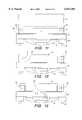
- FIG. 6Aa perspective view of a heat sink embodiment of the invention is shown.
- the heat sink 8comprises a flat, square, horizontal base member and four vertical heat exchanging fins which extend perpendicularly from the base member.
- the size and shape of the base member of the heat sink 8is similar to the outside dimension of the stiffener shown in FIGS. 4A through 4C.
- the heat sinkcomprises pins 14 which protrude perpendicularly from the lower surface of the base member. While four pins 14 are shown, alternative embodiments comprise any number of pins.
- FIG. 6Bis a perspective view of a stiffener 11 attached to a package substrate 2. Encapsulant 6 is filled into the inner opening of the stiffener.
- the stiffenercomprises four holes 12, one at the center of each side of the stiffener 11.
- FIG. 6Cis a perspective view of the heat sink 8 of FIG. 6A attached to the stiffener 11 of FIG. 6B.
Landscapes
- Engineering & Computer Science (AREA)
- Physics & Mathematics (AREA)
- Condensed Matter Physics & Semiconductors (AREA)
- General Physics & Mathematics (AREA)
- Computer Hardware Design (AREA)
- Microelectronics & Electronic Packaging (AREA)
- Power Engineering (AREA)
- Chemical & Material Sciences (AREA)
- Materials Engineering (AREA)
- Cooling Or The Like Of Semiconductors Or Solid State Devices (AREA)
Abstract
Description
Claims (19)
Priority Applications (1)
| Application Number | Priority Date | Filing Date | Title |
|---|---|---|---|
| US08/850,292US6011304A (en) | 1997-05-05 | 1997-05-05 | Stiffener ring attachment with holes and removable snap-in heat sink or heat spreader/lid |
Applications Claiming Priority (1)
| Application Number | Priority Date | Filing Date | Title |
|---|---|---|---|
| US08/850,292US6011304A (en) | 1997-05-05 | 1997-05-05 | Stiffener ring attachment with holes and removable snap-in heat sink or heat spreader/lid |
Publications (1)
| Publication Number | Publication Date |
|---|---|
| US6011304Atrue US6011304A (en) | 2000-01-04 |
Family
ID=25307752
Family Applications (1)
| Application Number | Title | Priority Date | Filing Date |
|---|---|---|---|
| US08/850,292Expired - LifetimeUS6011304A (en) | 1997-05-05 | 1997-05-05 | Stiffener ring attachment with holes and removable snap-in heat sink or heat spreader/lid |
Country Status (1)
| Country | Link |
|---|---|
| US (1) | US6011304A (en) |
Cited By (101)
| Publication number | Priority date | Publication date | Assignee | Title |
|---|---|---|---|---|
| US6097101A (en)* | 1998-01-30 | 2000-08-01 | Shinko Electric Industries Co., Ltd. | Package for semiconductor device having frame-like molded portion and producing method of the same |
| US6188579B1 (en)* | 1999-07-12 | 2001-02-13 | Lucent Technologies Inc. | Apparatus and methods for forming a printed wiring board assembly to reduce pallet warpage |
| US6229702B1 (en)* | 1999-06-02 | 2001-05-08 | Advanced Semiconductor Engineering, Inc. | Ball grid array semiconductor package having improved heat dissipation efficiency, overall electrical performance and enhanced bonding capability |
| US6262479B1 (en)* | 1999-10-05 | 2001-07-17 | Pan Pacific Semiconductor Co., Ltd. | Semiconductor packaging structure |
| US6261871B1 (en)* | 1999-03-11 | 2001-07-17 | Conexant Systems, Inc. | Method and structure for temperature stabilization in flip chip technology |
| US6278613B1 (en) | 2000-09-27 | 2001-08-21 | St Assembly Test Services Pte Ltd | Copper pads for heat spreader attach |
| US6320754B1 (en)* | 1999-08-06 | 2001-11-20 | Agilent Technologies, Inc. | Apparatus for the reduction of interfacial stress caused by differential thermal expansion in an integrated circuit package |
| US20020052105A1 (en)* | 1999-08-31 | 2002-05-02 | Salman Akram | Chip package with grease heat sink and method of making |
| US6403401B1 (en) | 2000-08-14 | 2002-06-11 | St Assembly Test Services Pte Ltd | Heat spreader hole pin 1 identifier |
| US6407334B1 (en)* | 2000-11-30 | 2002-06-18 | International Business Machines Corporation | I/C chip assembly |
| US6432742B1 (en) | 2000-08-17 | 2002-08-13 | St Assembly Test Services Pte Ltd. | Methods of forming drop-in heat spreader plastic ball grid array (PBGA) packages |
| US20020135065A1 (en)* | 2000-12-01 | 2002-09-26 | Zhao Sam Ziqun | Thermally and electrically enhanced ball grid array packaging |
| US20020149092A1 (en)* | 2001-04-11 | 2002-10-17 | Lee Ki Wook | Carrier frame and semiconductor package including carrier frame |
| US6472741B1 (en)* | 2001-07-14 | 2002-10-29 | Siliconware Precision Industries Co., Ltd. | Thermally-enhanced stacked-die ball grid array semiconductor package and method of fabricating the same |
| US6483706B2 (en)* | 2000-12-22 | 2002-11-19 | Vlt Corporation | Heat dissipation for electronic components |
| US6489557B2 (en)* | 1999-08-30 | 2002-12-03 | Intel Corporation | Implementing micro BGA™ assembly techniques for small die |
| US20020185722A1 (en)* | 2000-12-22 | 2002-12-12 | Zhao Sam Ziqun | Die-up ball grid array package with enhanced stiffener |
| US6515360B2 (en)* | 1999-07-28 | 2003-02-04 | Mitsubishi Denki Kabushiki Kaisha | Packaged semiconductor device and manufacturing method thereof |
| US20030057550A1 (en)* | 2000-12-22 | 2003-03-27 | Broadcom Corporation | Ball grid array package enhanced with a thermal and electrical connector |
| US20030111726A1 (en)* | 2001-12-18 | 2003-06-19 | Khan Reza-Ur Rahman | Ball grid array package substrates and method of making the same |
| US20030146503A1 (en)* | 2002-02-01 | 2003-08-07 | Broadcom Corporation | Ball grid array package with stepped stiffener layer |
| US20030146506A1 (en)* | 2002-02-01 | 2003-08-07 | Broadcom Corporation | Ball grid array package fabrication with IC die support structures |
| US20030146511A1 (en)* | 2002-02-01 | 2003-08-07 | Broadcom Corporation | Ball grid array package with multiple interposers |
| US6608283B2 (en)* | 2000-02-08 | 2003-08-19 | Emagin Corporation | Apparatus and method for solder-sealing an active matrix organic light emitting diode |
| US6607942B1 (en) | 2001-07-26 | 2003-08-19 | Taiwan Semiconductor Manufacturing Company | Method of fabricating as grooved heat spreader for stress reduction in an IC package |
| US20030179556A1 (en)* | 2002-03-21 | 2003-09-25 | Broadcom Corporation | Enhanced die-up ball grid array package with two substrates and method for making the same |
| US20030178719A1 (en)* | 2002-03-22 | 2003-09-25 | Combs Edward G. | Enhanced thermal dissipation integrated circuit package and method of manufacturing enhanced thermal dissipation integrated circuit package |
| US20030179549A1 (en)* | 2002-03-22 | 2003-09-25 | Zhong Chong Hua | Low voltage drop and high thermal perfor mance ball grid array package |
| US6655022B1 (en) | 1998-09-24 | 2003-12-02 | Intel Corporation | Implementing micro BGA assembly techniques for small die |
| US20040036162A1 (en)* | 2002-08-21 | 2004-02-26 | Shih-Fang Chuang | Integrated circuit package with heatsink support |
| US20040037059A1 (en)* | 2002-08-21 | 2004-02-26 | Leon Stiborek | Integrated circuit package with spacer |
| US6724080B1 (en)* | 2002-12-20 | 2004-04-20 | Altera Corporation | Heat sink with elevated heat spreader lid |
| US6734552B2 (en) | 2001-07-11 | 2004-05-11 | Asat Limited | Enhanced thermal dissipation integrated circuit package |
| US6747346B2 (en)* | 2001-04-12 | 2004-06-08 | Fuji Electric Co., Ltd. | Container for semiconductor sensor, manufacturing method therefor, and semiconductor sensor device |
| US6787900B2 (en)* | 1999-10-27 | 2004-09-07 | Mitsubishi Denki Kabushiki Kaisha | Semiconductor module and insulating substrate thereof |
| US20040174682A1 (en)* | 2003-03-04 | 2004-09-09 | Siliconware Precision Industries, Ltd. | Semiconductor package with heat sink |
| US20040178494A1 (en)* | 2003-03-11 | 2004-09-16 | Silicinware Precision Industries, Ltd | Semiconductor package with heat sink |
| US20040212051A1 (en)* | 2000-12-22 | 2004-10-28 | Broadcom Corporation | Ball grid array package with patterned stiffener layer |
| US20050012189A1 (en)* | 2002-08-16 | 2005-01-20 | Ho Kwun Yao | Integrated circuit package with a balanced-part structure |
| US20050012203A1 (en)* | 2001-02-15 | 2005-01-20 | Rahman Khan Reza-Ur | Enhanced die-down ball grid array and method for making the same |
| US6856015B1 (en) | 2003-08-21 | 2005-02-15 | Siliconware Precision Industries Co., Ltd. | Semiconductor package with heat sink |
| US20050034841A1 (en)* | 2003-08-13 | 2005-02-17 | Barr Andrew Harvey | Integral chip lid and heat sink |
| US20050051890A1 (en)* | 2001-05-07 | 2005-03-10 | Broadcom Corporation | Die-up ball grid array package including a substrate capable of mounting an integrated circuit die and method for making the same |
| US6903278B2 (en)* | 2001-06-29 | 2005-06-07 | Intel Corporation | Arrangements to provide mechanical stiffening elements to a thin-core or coreless substrate |
| US20050127502A1 (en)* | 2003-12-16 | 2005-06-16 | Taiwan Semiconductor Manufacturing Co., Ltd. | Thermal dispensing enhancement for high performance flip chip BGA (HPFCBGA) |
| US20050161816A1 (en)* | 2003-03-26 | 2005-07-28 | Fujitsu Limited | Semiconductor device |
| US20050170561A1 (en)* | 2004-02-04 | 2005-08-04 | Siliconware Precision Industries Co. Ltd., Taiwan, R.O.C. | Fabrication method of semiconductor package with photosensitive chip |
| US20050173792A1 (en)* | 2004-02-10 | 2005-08-11 | Uniwill Computer Corp. | Structure for isolating thermal interface material |
| US20050199998A1 (en)* | 2004-03-09 | 2005-09-15 | Siliconware Precision Industries Co., Ltd. | Semiconductor package with heat sink and method for fabricating the same and stiffener |
| US20050280139A1 (en)* | 2004-06-21 | 2005-12-22 | Broadcom Corporation | Multipiece apparatus for thermal and electromagnetic interference (EMI) shielding enhancement in die-up array packages and method of making the same |
| US20050280141A1 (en)* | 2004-06-21 | 2005-12-22 | Broadcom Corporation | Integrated circuit device package having both wire bond and flip-chip interconnections and method of making the same |
| US20060043553A1 (en)* | 2004-09-02 | 2006-03-02 | Advanced Semiconductor Engineering, Inc. | Chip package having a heat spreader and method for packaging the same |
| US7015072B2 (en) | 2001-07-11 | 2006-03-21 | Asat Limited | Method of manufacturing an enhanced thermal dissipation integrated circuit package |
| US20060065972A1 (en)* | 2004-09-29 | 2006-03-30 | Broadcom Corporation | Die down ball grid array packages and method for making same |
| US20060125089A1 (en)* | 2002-12-19 | 2006-06-15 | Tatt Koay H | Thermally enhanced package for an integrated circuit |
| US20060137902A1 (en)* | 2004-12-27 | 2006-06-29 | Fujitsu Limited | Semiconductor device and manufacturing method therefor |
| US20060170094A1 (en)* | 2005-02-02 | 2006-08-03 | Intel Corporation | Semiconductor package integral heat spreader |
| US7132744B2 (en) | 2000-12-22 | 2006-11-07 | Broadcom Corporation | Enhanced die-up ball grid array packages and method for making the same |
| US20070120149A1 (en)* | 2001-09-28 | 2007-05-31 | Intel Corporation | Package stiffener |
| US20070145571A1 (en)* | 2005-12-15 | 2007-06-28 | Taiwan Semiconductor Manufacturing Co., Ltd. | Semiconductor package structure with constraint stiffener for cleaning and underfilling efficiency |
| US20070200228A1 (en)* | 2006-02-27 | 2007-08-30 | Siliconware Precision Industries Co., Ltd. | Semiconductor package having heat dissipating device and fabrication method of the semiconductor package |
| US20070215997A1 (en)* | 2006-03-17 | 2007-09-20 | Martin Standing | Chip-scale package |
| US20070235861A1 (en)* | 2006-04-06 | 2007-10-11 | Siliconware Precision Industries Co., Ltd. | Semiconductor device package with a heat sink and method for fabricating the same |
| US20070267734A1 (en)* | 2006-05-16 | 2007-11-22 | Broadcom Corporation | No-lead IC packages having integrated heat spreader for electromagnetic interference (EMI) shielding and thermal enhancement |
| CN100359676C (en)* | 2002-04-05 | 2008-01-02 | 英特尔公司 | Heat spreader with down set leg attachment feature |
| WO2007117819A3 (en)* | 2006-04-06 | 2008-01-17 | Freescale Semiconductor Inc | Molded semiconductor package with integrated through hole heat spreader pin(s) |
| CN100380641C (en)* | 2001-09-28 | 2008-04-09 | 英特尔公司 | Arrangements to increase structural rigidity of semiconductor package |
| US20080162045A1 (en)* | 2006-12-29 | 2008-07-03 | Hung-Fu Lee | Traffic flow and vehicle position detection system |
| US20080227310A1 (en)* | 2007-03-16 | 2008-09-18 | Seah Sun Too | Integrated Circuit Socket |
| US7432586B2 (en) | 2004-06-21 | 2008-10-07 | Broadcom Corporation | Apparatus and method for thermal and electromagnetic interference (EMI) shielding enhancement in die-up array packages |
| US20090052483A1 (en)* | 2007-08-20 | 2009-02-26 | Young Optics Inc. | Optoelectronic semiconductor package and method for attaching heat dissipation element thereto |
| US7518233B1 (en)* | 1999-06-09 | 2009-04-14 | Hitachi, Ltd. | Sealing structure for multi-chip module |
| US7550845B2 (en) | 2002-02-01 | 2009-06-23 | Broadcom Corporation | Ball grid array package with separated stiffener layer |
| US20100072564A1 (en)* | 2005-12-06 | 2010-03-25 | Yamaha Corporation | Semiconductor device and manufacturing method thereof |
| US20110001225A1 (en)* | 2007-12-03 | 2011-01-06 | Panasonic Corporation | Semiconductor device and method for manufacturing the same |
| US20110018125A1 (en)* | 2009-07-21 | 2011-01-27 | Stmicroelectronics Asia Pacific Pte Ltd (Singapore) | Semiconductor package with a stiffening member supporting a thermal heat spreader |
| EP2248165A4 (en)* | 2008-02-28 | 2012-04-18 | Lsi Corp | METHOD FOR GROUNDING A THERMAL DISSIPATOR OR STIFFENER ON A PROTUBERANCE CHIP MODULE USING THE SOLDER AND A FILM ADHESIVE |
| US8425246B1 (en) | 2011-12-01 | 2013-04-23 | Advanced Micro Devices, Inc. | Low profile semiconductor device socket |
| US8492888B2 (en) | 2011-09-02 | 2013-07-23 | Stats Chippac Ltd. | Integrated circuit packaging system with stiffener and method of manufacture thereof |
| US8610262B1 (en)* | 2005-02-18 | 2013-12-17 | Utac Hong Kong Limited | Ball grid array package with improved thermal characteristics |
| US20140008739A1 (en)* | 2010-03-11 | 2014-01-09 | Freescale Semiconductor, Inc. | Semiconductor device and method of fabricating same |
| US8679900B2 (en) | 2011-12-14 | 2014-03-25 | Stats Chippac Ltd. | Integrated circuit packaging system with heat conduction and method of manufacture thereof |
| US20140151871A1 (en)* | 2012-12-04 | 2014-06-05 | General Electric Company | Heat spreader with flexible tolerance mechanism |
| US8837162B2 (en) | 2010-05-06 | 2014-09-16 | Advanced Micro Devices, Inc. | Circuit board socket with support structure |
| US20150015779A1 (en)* | 2013-07-12 | 2015-01-15 | Hon Hai Precision Industry Co., Ltd. | Camera module |
| US20150021754A1 (en)* | 2009-11-25 | 2015-01-22 | Stats Chippac, Ltd. | Semiconductor Device and Method of Forming Thermal Lid for Balancing Warpage and Thermal Management |
| US8938876B2 (en) | 2010-05-06 | 2015-01-27 | Advanced Micro Devices, Inc. | Method of mounting a circuit board |
| US9305889B2 (en) | 2009-03-09 | 2016-04-05 | Utac Hong Kong Limited | Leadless integrated circuit package having standoff contacts and die attach pad |
| US9508621B2 (en) | 2009-11-25 | 2016-11-29 | STATS ChipPAC Pte. Ltd. | Semiconductor device and method of forming compliant stress relief buffer around large array WLCSP |
| US20170092619A1 (en)* | 2015-09-28 | 2017-03-30 | Xilinx, Inc. | Stacked silicon package assembly having an enhanced lid |
| WO2017111839A1 (en)* | 2015-12-26 | 2017-06-29 | Intel Corporation | Swaging process for complex integrated heat spreaders |
| US10049896B2 (en) | 2015-12-09 | 2018-08-14 | International Business Machines Corporation | Lid attach optimization to limit electronic package warpage |
| WO2019034246A1 (en)* | 2017-08-16 | 2019-02-21 | Arcelik Anonim Sirketi | Surface mount heat sinks for printed circuit boards and assembly method thereof |
| US20190172767A1 (en)* | 2017-12-06 | 2019-06-06 | Google Llc | Apparatus and mechanisms for reducing warpage and increasing surface mount technology yields in high performance integrated circuit packages |
| US10461003B2 (en) | 2015-12-14 | 2019-10-29 | Intel Corporation | Electronic package that includes multiple supports |
| US10764996B1 (en)* | 2018-06-19 | 2020-09-01 | Xilinx, Inc. | Chip package assembly with composite stiffener |
| US11373929B1 (en) | 2020-02-03 | 2022-06-28 | Xilinx, Inc. | Thermal heat spreader plate for electronic device |
| US20230010169A1 (en)* | 2021-07-07 | 2023-01-12 | Mitsubishi Electric Corporation | Semiconductor device and inverter device |
| US20240290682A1 (en)* | 2021-02-26 | 2024-08-29 | Taiwan Semiconductor Manufacturing Company, Ltd. | Package structure with buffer layer embedded in lid layer |
| EP4398297A3 (en)* | 2020-05-19 | 2024-10-30 | Google LLC | Weight optimized stiffener and sealing structure for direct liquid cooled modules |
| US12368114B2 (en)* | 2021-05-12 | 2025-07-22 | Taiwan Semiconductor Manufacturing Company, Ltd. | Semiconductor device package having warpage control and method of forming the same |
Citations (20)
| Publication number | Priority date | Publication date | Assignee | Title |
|---|---|---|---|---|
| JPS5965457A (en)* | 1982-10-05 | 1984-04-13 | Mitsubishi Electric Corp | Semiconductor device |
| JPS6237950A (en)* | 1985-08-12 | 1987-02-18 | Matsushita Electronics Corp | Electronic-part mounting package |
| JPS63293958A (en)* | 1987-05-27 | 1988-11-30 | Hitachi Ltd | Electronic device |
| JPS6457738A (en)* | 1987-08-28 | 1989-03-06 | Sumitomo Electric Industries | Package for semiconductor device |
| JPH02205347A (en)* | 1989-02-03 | 1990-08-15 | Mitsubishi Electric Corp | Semiconductor device |
| JPH02246142A (en)* | 1989-03-17 | 1990-10-01 | Fujitsu Ltd | semiconductor equipment |
| JPH04116853A (en)* | 1990-09-06 | 1992-04-17 | Murata Mfg Co Ltd | Electronic parts packaging method |
| JPH04186752A (en)* | 1990-11-21 | 1992-07-03 | Hitachi Ltd | How to remove heat sinks from electronic devices |
| US5182632A (en)* | 1989-11-22 | 1993-01-26 | Tactical Fabs, Inc. | High density multichip package with interconnect structure and heatsink |
| US5227663A (en)* | 1989-12-19 | 1993-07-13 | Lsi Logic Corporation | Integral dam and heat sink for semiconductor device assembly |
| US5230759A (en)* | 1989-10-20 | 1993-07-27 | Fujitsu Limited | Process for sealing a semiconductor device |
| JPH05267485A (en)* | 1992-03-24 | 1993-10-15 | Toshiba Corp | Dustproof housing for semiconductor devices |
| JPH06120366A (en)* | 1992-10-06 | 1994-04-28 | Sony Corp | Semiconductor device |
| US5384940A (en)* | 1992-02-28 | 1995-01-31 | Aavid Engineering, Inc. | Self-locking heat sinks for surface mount devices |
| US5455462A (en)* | 1992-01-17 | 1995-10-03 | Amkor Electronics, Inc. | Plastic molded package with heat sink for integrated circuit devices |
| US5552635A (en)* | 1994-01-11 | 1996-09-03 | Samsung Electronics Co., Ltd. | High thermal emissive semiconductor device package |
| US5619399A (en)* | 1995-02-16 | 1997-04-08 | Micromodule Systems, Inc. | Multiple chip module mounting assembly and computer using same |
| US5625222A (en)* | 1993-11-18 | 1997-04-29 | Fujitsu Limited | Semiconductor device in a resin package housed in a frame having high thermal conductivity |
| US5642265A (en)* | 1994-11-29 | 1997-06-24 | Sgs-Thomson Microelectronics, Inc. | Ball grid array package with detachable module |
| US5691041A (en)* | 1995-09-29 | 1997-11-25 | International Business Machines Corporation | Socket for semi-permanently connecting a solder ball grid array device using a dendrite interposer |
- 1997
- 1997-05-05USUS08/850,292patent/US6011304A/ennot_activeExpired - Lifetime
Patent Citations (20)
| Publication number | Priority date | Publication date | Assignee | Title |
|---|---|---|---|---|
| JPS5965457A (en)* | 1982-10-05 | 1984-04-13 | Mitsubishi Electric Corp | Semiconductor device |
| JPS6237950A (en)* | 1985-08-12 | 1987-02-18 | Matsushita Electronics Corp | Electronic-part mounting package |
| JPS63293958A (en)* | 1987-05-27 | 1988-11-30 | Hitachi Ltd | Electronic device |
| JPS6457738A (en)* | 1987-08-28 | 1989-03-06 | Sumitomo Electric Industries | Package for semiconductor device |
| JPH02205347A (en)* | 1989-02-03 | 1990-08-15 | Mitsubishi Electric Corp | Semiconductor device |
| JPH02246142A (en)* | 1989-03-17 | 1990-10-01 | Fujitsu Ltd | semiconductor equipment |
| US5230759A (en)* | 1989-10-20 | 1993-07-27 | Fujitsu Limited | Process for sealing a semiconductor device |
| US5182632A (en)* | 1989-11-22 | 1993-01-26 | Tactical Fabs, Inc. | High density multichip package with interconnect structure and heatsink |
| US5227663A (en)* | 1989-12-19 | 1993-07-13 | Lsi Logic Corporation | Integral dam and heat sink for semiconductor device assembly |
| JPH04116853A (en)* | 1990-09-06 | 1992-04-17 | Murata Mfg Co Ltd | Electronic parts packaging method |
| JPH04186752A (en)* | 1990-11-21 | 1992-07-03 | Hitachi Ltd | How to remove heat sinks from electronic devices |
| US5455462A (en)* | 1992-01-17 | 1995-10-03 | Amkor Electronics, Inc. | Plastic molded package with heat sink for integrated circuit devices |
| US5384940A (en)* | 1992-02-28 | 1995-01-31 | Aavid Engineering, Inc. | Self-locking heat sinks for surface mount devices |
| JPH05267485A (en)* | 1992-03-24 | 1993-10-15 | Toshiba Corp | Dustproof housing for semiconductor devices |
| JPH06120366A (en)* | 1992-10-06 | 1994-04-28 | Sony Corp | Semiconductor device |
| US5625222A (en)* | 1993-11-18 | 1997-04-29 | Fujitsu Limited | Semiconductor device in a resin package housed in a frame having high thermal conductivity |
| US5552635A (en)* | 1994-01-11 | 1996-09-03 | Samsung Electronics Co., Ltd. | High thermal emissive semiconductor device package |
| US5642265A (en)* | 1994-11-29 | 1997-06-24 | Sgs-Thomson Microelectronics, Inc. | Ball grid array package with detachable module |
| US5619399A (en)* | 1995-02-16 | 1997-04-08 | Micromodule Systems, Inc. | Multiple chip module mounting assembly and computer using same |
| US5691041A (en)* | 1995-09-29 | 1997-11-25 | International Business Machines Corporation | Socket for semi-permanently connecting a solder ball grid array device using a dendrite interposer |
Cited By (208)
| Publication number | Priority date | Publication date | Assignee | Title |
|---|---|---|---|---|
| US6097101A (en)* | 1998-01-30 | 2000-08-01 | Shinko Electric Industries Co., Ltd. | Package for semiconductor device having frame-like molded portion and producing method of the same |
| US6655022B1 (en) | 1998-09-24 | 2003-12-02 | Intel Corporation | Implementing micro BGA assembly techniques for small die |
| US6261871B1 (en)* | 1999-03-11 | 2001-07-17 | Conexant Systems, Inc. | Method and structure for temperature stabilization in flip chip technology |
| US6229702B1 (en)* | 1999-06-02 | 2001-05-08 | Advanced Semiconductor Engineering, Inc. | Ball grid array semiconductor package having improved heat dissipation efficiency, overall electrical performance and enhanced bonding capability |
| US7518233B1 (en)* | 1999-06-09 | 2009-04-14 | Hitachi, Ltd. | Sealing structure for multi-chip module |
| US6188579B1 (en)* | 1999-07-12 | 2001-02-13 | Lucent Technologies Inc. | Apparatus and methods for forming a printed wiring board assembly to reduce pallet warpage |
| US6515360B2 (en)* | 1999-07-28 | 2003-02-04 | Mitsubishi Denki Kabushiki Kaisha | Packaged semiconductor device and manufacturing method thereof |
| US6320754B1 (en)* | 1999-08-06 | 2001-11-20 | Agilent Technologies, Inc. | Apparatus for the reduction of interfacial stress caused by differential thermal expansion in an integrated circuit package |
| US6489557B2 (en)* | 1999-08-30 | 2002-12-03 | Intel Corporation | Implementing micro BGA™ assembly techniques for small die |
| US20060097381A1 (en)* | 1999-08-31 | 2006-05-11 | Salman Akram | Chip package with grease heat sink |
| US20020052105A1 (en)* | 1999-08-31 | 2002-05-02 | Salman Akram | Chip package with grease heat sink and method of making |
| US20050221533A1 (en)* | 1999-08-31 | 2005-10-06 | Salman Akram | Method of making chip package with grease heat sink |
| US6424033B1 (en)* | 1999-08-31 | 2002-07-23 | Micron Technology, Inc. | Chip package with grease heat sink and method of making |
| US6919220B2 (en)* | 1999-08-31 | 2005-07-19 | Micron Technology, Inc. | Method of making chip package with grease heat sink |
| US6794749B2 (en) | 1999-08-31 | 2004-09-21 | Micron Technology, Inc. | Chip package with grease heat sink |
| US20050001312A1 (en)* | 1999-08-31 | 2005-01-06 | Micron Technology | Chip package with grease heat sink |
| US6262479B1 (en)* | 1999-10-05 | 2001-07-17 | Pan Pacific Semiconductor Co., Ltd. | Semiconductor packaging structure |
| US6787900B2 (en)* | 1999-10-27 | 2004-09-07 | Mitsubishi Denki Kabushiki Kaisha | Semiconductor module and insulating substrate thereof |
| US6608283B2 (en)* | 2000-02-08 | 2003-08-19 | Emagin Corporation | Apparatus and method for solder-sealing an active matrix organic light emitting diode |
| US6403401B1 (en) | 2000-08-14 | 2002-06-11 | St Assembly Test Services Pte Ltd | Heat spreader hole pin 1 identifier |
| US6750534B2 (en) | 2000-08-14 | 2004-06-15 | St Assembly Test Services Ltd | Heat spreader hole pin 1 identifier |
| US6432742B1 (en) | 2000-08-17 | 2002-08-13 | St Assembly Test Services Pte Ltd. | Methods of forming drop-in heat spreader plastic ball grid array (PBGA) packages |
| US6278613B1 (en) | 2000-09-27 | 2001-08-21 | St Assembly Test Services Pte Ltd | Copper pads for heat spreader attach |
| US6407334B1 (en)* | 2000-11-30 | 2002-06-18 | International Business Machines Corporation | I/C chip assembly |
| US20050077545A1 (en)* | 2000-12-01 | 2005-04-14 | Broadcom Corporation | Ball grid array package with patterned stiffener surface and method of assembling the same |
| US6882042B2 (en)* | 2000-12-01 | 2005-04-19 | Broadcom Corporation | Thermally and electrically enhanced ball grid array packaging |
| US8686558B2 (en) | 2000-12-01 | 2014-04-01 | Broadcom Corporation | Thermally and electrically enhanced ball grid array package |
| US8039949B2 (en) | 2000-12-01 | 2011-10-18 | Broadcom Corporation | Ball grid array package having one or more stiffeners |
| US20020135065A1 (en)* | 2000-12-01 | 2002-09-26 | Zhao Sam Ziqun | Thermally and electrically enhanced ball grid array packaging |
| US7629681B2 (en) | 2000-12-01 | 2009-12-08 | Broadcom Corporation | Ball grid array package with patterned stiffener surface and method of assembling the same |
| US20100052151A1 (en)* | 2000-12-01 | 2010-03-04 | Broadcom Corporation | Ball Grid Array Package Having One or More Stiffeners |
| US20030057550A1 (en)* | 2000-12-22 | 2003-03-27 | Broadcom Corporation | Ball grid array package enhanced with a thermal and electrical connector |
| US6906414B2 (en) | 2000-12-22 | 2005-06-14 | Broadcom Corporation | Ball grid array package with patterned stiffener layer |
| US7893546B2 (en) | 2000-12-22 | 2011-02-22 | Broadcom Corporation | Ball grid array package enhanced with a thermal and electrical connector |
| US7579217B2 (en) | 2000-12-22 | 2009-08-25 | Broadcom Corporation | Methods of making a die-up ball grid array package with printed circuit board attachable heat spreader |
| US20090203172A1 (en)* | 2000-12-22 | 2009-08-13 | Broadcom Corporation | Enhanced Die-Up Ball Grid Array and Method for Making the Same |
| US7005737B2 (en) | 2000-12-22 | 2006-02-28 | Broadcom Corporation | Die-up ball grid array package with enhanced stiffener |
| US7038312B2 (en) | 2000-12-22 | 2006-05-02 | Broadcom Corporation | Die-up ball grid array package with attached stiffener ring |
| US20110140272A1 (en)* | 2000-12-22 | 2011-06-16 | Broadcom Corporation | Ball Grid Array Package Enhanced With a Thermal and Electrical Connector |
| US7102225B2 (en) | 2000-12-22 | 2006-09-05 | Broadcom Corporation | Die-up ball grid array package with printed circuit board attachable heat spreader |
| US7132744B2 (en) | 2000-12-22 | 2006-11-07 | Broadcom Corporation | Enhanced die-up ball grid array packages and method for making the same |
| US6483706B2 (en)* | 2000-12-22 | 2002-11-19 | Vlt Corporation | Heat dissipation for electronic components |
| US20090057871A1 (en)* | 2000-12-22 | 2009-03-05 | Broadcom Corporation | Ball Grid Array Package Enhanced With a Thermal and Electrical Connector |
| US7462933B2 (en) | 2000-12-22 | 2008-12-09 | Broadcom Corporation | Ball grid array package enhanced with a thermal and electrical connector |
| US8310067B2 (en) | 2000-12-22 | 2012-11-13 | Broadcom Corporation | Ball grid array package enhanced with a thermal and electrical connector |
| US20040212051A1 (en)* | 2000-12-22 | 2004-10-28 | Broadcom Corporation | Ball grid array package with patterned stiffener layer |
| US20050133905A1 (en)* | 2000-12-22 | 2005-06-23 | Broadcom Corporation | Method of assembling a ball grid array package with patterned stiffener layer |
| US7161239B2 (en) | 2000-12-22 | 2007-01-09 | Broadcom Corporation | Ball grid array package enhanced with a thermal and electrical connector |
| US7859101B2 (en) | 2000-12-22 | 2010-12-28 | Broadcom Corporation | Die-up ball grid array package with die-attached heat spreader |
| US20070045824A1 (en)* | 2000-12-22 | 2007-03-01 | Broadcom Corporation | Methods of making a die-up ball grid array package with printed circuit board attachable heat spreader |
| US20020185722A1 (en)* | 2000-12-22 | 2002-12-12 | Zhao Sam Ziqun | Die-up ball grid array package with enhanced stiffener |
| US6989593B2 (en) | 2000-12-22 | 2006-01-24 | Broadcom Corporation | Die-up ball grid array package with patterned stiffener opening |
| US7202559B2 (en) | 2000-12-22 | 2007-04-10 | Broadcom Corporation | Method of assembling a ball grid array package with patterned stiffener layer |
| US20050029657A1 (en)* | 2000-12-22 | 2005-02-10 | Broadcom Corporation | Enhanced die-up ball grid array and method for making the same |
| US7227256B2 (en) | 2000-12-22 | 2007-06-05 | Broadcom Corporation | Die-up ball grid array package with printed circuit board attachable heat spreader |
| EP1225631A3 (en)* | 2000-12-22 | 2003-06-04 | Vlt Corporation | Heat dissipation arrangement for electronic components |
| US20050012203A1 (en)* | 2001-02-15 | 2005-01-20 | Rahman Khan Reza-Ur | Enhanced die-down ball grid array and method for making the same |
| US6853070B2 (en) | 2001-02-15 | 2005-02-08 | Broadcom Corporation | Die-down ball grid array package with die-attached heat spreader and method for making the same |
| US7402906B2 (en) | 2001-02-15 | 2008-07-22 | Broadcom Corporation | Enhanced die-down ball grid array and method for making the same |
| US20020149092A1 (en)* | 2001-04-11 | 2002-10-17 | Lee Ki Wook | Carrier frame and semiconductor package including carrier frame |
| US6770961B2 (en)* | 2001-04-11 | 2004-08-03 | Amkor Technology, Inc. | Carrier frame and semiconductor package including carrier frame |
| US6747346B2 (en)* | 2001-04-12 | 2004-06-08 | Fuji Electric Co., Ltd. | Container for semiconductor sensor, manufacturing method therefor, and semiconductor sensor device |
| US7259448B2 (en)* | 2001-05-07 | 2007-08-21 | Broadcom Corporation | Die-up ball grid array package with a heat spreader and method for making the same |
| US20050051890A1 (en)* | 2001-05-07 | 2005-03-10 | Broadcom Corporation | Die-up ball grid array package including a substrate capable of mounting an integrated circuit die and method for making the same |
| US7259457B2 (en) | 2001-05-07 | 2007-08-21 | Broadcom Corporation | Die-up ball grid array package including a substrate capable of mounting an integrated circuit die and method for making the same |
| US6903278B2 (en)* | 2001-06-29 | 2005-06-07 | Intel Corporation | Arrangements to provide mechanical stiffening elements to a thin-core or coreless substrate |
| US7015072B2 (en) | 2001-07-11 | 2006-03-21 | Asat Limited | Method of manufacturing an enhanced thermal dissipation integrated circuit package |
| US6734552B2 (en) | 2001-07-11 | 2004-05-11 | Asat Limited | Enhanced thermal dissipation integrated circuit package |
| US6472741B1 (en)* | 2001-07-14 | 2002-10-29 | Siliconware Precision Industries Co., Ltd. | Thermally-enhanced stacked-die ball grid array semiconductor package and method of fabricating the same |
| US6607942B1 (en) | 2001-07-26 | 2003-08-19 | Taiwan Semiconductor Manufacturing Company | Method of fabricating as grooved heat spreader for stress reduction in an IC package |
| US20030176020A1 (en)* | 2001-07-26 | 2003-09-18 | Pei-Haw Tsao | Grooved heat spreader for stress reduction in IC package |
| CN100380641C (en)* | 2001-09-28 | 2008-04-09 | 英特尔公司 | Arrangements to increase structural rigidity of semiconductor package |
| US20070120149A1 (en)* | 2001-09-28 | 2007-05-31 | Intel Corporation | Package stiffener |
| US20030111726A1 (en)* | 2001-12-18 | 2003-06-19 | Khan Reza-Ur Rahman | Ball grid array package substrates and method of making the same |
| US7405145B2 (en) | 2001-12-18 | 2008-07-29 | Broadcom Corporation | Ball grid array package substrates with a modified central opening and method for making the same |
| US6879039B2 (en) | 2001-12-18 | 2005-04-12 | Broadcom Corporation | Ball grid array package substrates and method of making the same |
| US7245500B2 (en) | 2002-02-01 | 2007-07-17 | Broadcom Corporation | Ball grid array package with stepped stiffener layer |
| US20030146511A1 (en)* | 2002-02-01 | 2003-08-07 | Broadcom Corporation | Ball grid array package with multiple interposers |
| US20040262754A1 (en)* | 2002-02-01 | 2004-12-30 | Khan Reza-Ur Rahman | IC die support structures for ball grid array package fabrication |
| US7078806B2 (en) | 2002-02-01 | 2006-07-18 | Broadcom Corporation | IC die support structures for ball grid array package fabrication |
| US20030146503A1 (en)* | 2002-02-01 | 2003-08-07 | Broadcom Corporation | Ball grid array package with stepped stiffener layer |
| US6861750B2 (en) | 2002-02-01 | 2005-03-01 | Broadcom Corporation | Ball grid array package with multiple interposers |
| US7241645B2 (en) | 2002-02-01 | 2007-07-10 | Broadcom Corporation | Method for assembling a ball grid array package with multiple interposers |
| US6825108B2 (en) | 2002-02-01 | 2004-11-30 | Broadcom Corporation | Ball grid array package fabrication with IC die support structures |
| US7550845B2 (en) | 2002-02-01 | 2009-06-23 | Broadcom Corporation | Ball grid array package with separated stiffener layer |
| US20030146506A1 (en)* | 2002-02-01 | 2003-08-07 | Broadcom Corporation | Ball grid array package fabrication with IC die support structures |
| US20030179556A1 (en)* | 2002-03-21 | 2003-09-25 | Broadcom Corporation | Enhanced die-up ball grid array package with two substrates and method for making the same |
| US20040113284A1 (en)* | 2002-03-21 | 2004-06-17 | Broadcom Corporation | Method for making an enhanced die-up ball grid array package with two substrates |
| US7312108B2 (en) | 2002-03-21 | 2007-12-25 | Broadcom Corporation | Method for assembling a ball grid array package with two substrates |
| US6876553B2 (en) | 2002-03-21 | 2005-04-05 | Broadcom Corporation | Enhanced die-up ball grid array package with two substrates |
| US6887741B2 (en) | 2002-03-21 | 2005-05-03 | Broadcom Corporation | Method for making an enhanced die-up ball grid array package with two substrates |
| US20040046241A1 (en)* | 2002-03-22 | 2004-03-11 | Combs Edward G. | Method of manufacturing enhanced thermal dissipation integrated circuit package |
| US20030178719A1 (en)* | 2002-03-22 | 2003-09-25 | Combs Edward G. | Enhanced thermal dissipation integrated circuit package and method of manufacturing enhanced thermal dissipation integrated circuit package |
| US7566590B2 (en) | 2002-03-22 | 2009-07-28 | Broadcom Corporation | Low voltage drop and high thermal performance ball grid array package |
| US7196415B2 (en) | 2002-03-22 | 2007-03-27 | Broadcom Corporation | Low voltage drop and high thermal performance ball grid array package |
| US20090267222A1 (en)* | 2002-03-22 | 2009-10-29 | Broadcom Corporation | Low Voltage Drop and High Thermal Performance Ball Grid Array Package |
| US7781882B2 (en)* | 2002-03-22 | 2010-08-24 | Broadcom Corporation | Low voltage drop and high thermal performance ball grid array package |
| US20030179549A1 (en)* | 2002-03-22 | 2003-09-25 | Zhong Chong Hua | Low voltage drop and high thermal perfor mance ball grid array package |
| CN100359676C (en)* | 2002-04-05 | 2008-01-02 | 英特尔公司 | Heat spreader with down set leg attachment feature |
| US7176559B2 (en)* | 2002-08-16 | 2007-02-13 | Via Technologies, Inc. | Integrated circuit package with a balanced-part structure |
| US20050012189A1 (en)* | 2002-08-16 | 2005-01-20 | Ho Kwun Yao | Integrated circuit package with a balanced-part structure |
| US20040036162A1 (en)* | 2002-08-21 | 2004-02-26 | Shih-Fang Chuang | Integrated circuit package with heatsink support |
| US20040037059A1 (en)* | 2002-08-21 | 2004-02-26 | Leon Stiborek | Integrated circuit package with spacer |
| US6936919B2 (en)* | 2002-08-21 | 2005-08-30 | Texas Instruments Incorporated | Heatsink-substrate-spacer structure for an integrated-circuit package |
| US7312525B2 (en)* | 2002-12-19 | 2007-12-25 | Avago Technologies General Ip (Singapore) Pte Ltd | Thermally enhanced package for an integrated circuit |
| US20060125089A1 (en)* | 2002-12-19 | 2006-06-15 | Tatt Koay H | Thermally enhanced package for an integrated circuit |
| US6724080B1 (en)* | 2002-12-20 | 2004-04-20 | Altera Corporation | Heat sink with elevated heat spreader lid |
| US20060017145A1 (en)* | 2003-03-04 | 2006-01-26 | Chang-Fu Lin | Semiconductor package with heat sink |
| US20040174682A1 (en)* | 2003-03-04 | 2004-09-09 | Siliconware Precision Industries, Ltd. | Semiconductor package with heat sink |
| US7196414B2 (en) | 2003-03-04 | 2007-03-27 | Siliconware Precision Industries Co., Ltd. | Semiconductor package with heat sink |
| US7177155B2 (en) | 2003-03-04 | 2007-02-13 | Siliconware Precision Industries Co., Ltd. | Semiconductor package with heat sink |
| US6849942B2 (en) | 2003-03-11 | 2005-02-01 | Siliconware Precision Industries Co., Ltd. | Semiconductor package with heat sink attached to substrate |
| US20040178494A1 (en)* | 2003-03-11 | 2004-09-16 | Silicinware Precision Industries, Ltd | Semiconductor package with heat sink |
| US20050161816A1 (en)* | 2003-03-26 | 2005-07-28 | Fujitsu Limited | Semiconductor device |
| US7102228B2 (en)* | 2003-03-26 | 2006-09-05 | Fujitsu Limited | Semiconductor device |
| US20050034841A1 (en)* | 2003-08-13 | 2005-02-17 | Barr Andrew Harvey | Integral chip lid and heat sink |
| US6856015B1 (en) | 2003-08-21 | 2005-02-15 | Siliconware Precision Industries Co., Ltd. | Semiconductor package with heat sink |
| US20050040519A1 (en)* | 2003-08-21 | 2005-02-24 | Siliconware Precision Industries | Semiconductor package with heat sink |
| US7026711B2 (en)* | 2003-12-16 | 2006-04-11 | Taiwan Semiconductor Manufacturing Company, Ltd. | Thermal dispensing enhancement for high performance flip chip BGA (HPFCBGA) |
| US20050127502A1 (en)* | 2003-12-16 | 2005-06-16 | Taiwan Semiconductor Manufacturing Co., Ltd. | Thermal dispensing enhancement for high performance flip chip BGA (HPFCBGA) |
| US20050170561A1 (en)* | 2004-02-04 | 2005-08-04 | Siliconware Precision Industries Co. Ltd., Taiwan, R.O.C. | Fabrication method of semiconductor package with photosensitive chip |
| US6989296B2 (en)* | 2004-02-04 | 2006-01-24 | Siliconware Precision Industries Co., Ltd. | Fabrication method of semiconductor package with photosensitive chip |
| US20050173792A1 (en)* | 2004-02-10 | 2005-08-11 | Uniwill Computer Corp. | Structure for isolating thermal interface material |
| US20050199998A1 (en)* | 2004-03-09 | 2005-09-15 | Siliconware Precision Industries Co., Ltd. | Semiconductor package with heat sink and method for fabricating the same and stiffener |
| US7482686B2 (en) | 2004-06-21 | 2009-01-27 | Braodcom Corporation | Multipiece apparatus for thermal and electromagnetic interference (EMI) shielding enhancement in die-up array packages and method of making the same |
| US7595227B2 (en) | 2004-06-21 | 2009-09-29 | Broadcom Corporation | Integrated circuit device package having both wire bond and flip-chip interconnections and method of making the same |
| US7432586B2 (en) | 2004-06-21 | 2008-10-07 | Broadcom Corporation | Apparatus and method for thermal and electromagnetic interference (EMI) shielding enhancement in die-up array packages |
| US20050280141A1 (en)* | 2004-06-21 | 2005-12-22 | Broadcom Corporation | Integrated circuit device package having both wire bond and flip-chip interconnections and method of making the same |
| US7791189B2 (en) | 2004-06-21 | 2010-09-07 | Broadcom Corporation | Multipiece apparatus for thermal and electromagnetic interference (EMI) shielding enhancement in die-up array packages and method of making the same |
| US7411281B2 (en) | 2004-06-21 | 2008-08-12 | Broadcom Corporation | Integrated circuit device package having both wire bond and flip-chip interconnections and method of making the same |
| US20050280139A1 (en)* | 2004-06-21 | 2005-12-22 | Broadcom Corporation | Multipiece apparatus for thermal and electromagnetic interference (EMI) shielding enhancement in die-up array packages and method of making the same |
| US20090115048A1 (en)* | 2004-06-21 | 2009-05-07 | Broadcom Corporation | Multipiece Apparatus for Thermal and Electromagnetic Interference (EMI) Shielding Enhancement in Die-Up Array Packages and Method of Making the Same |
| US20060043553A1 (en)* | 2004-09-02 | 2006-03-02 | Advanced Semiconductor Engineering, Inc. | Chip package having a heat spreader and method for packaging the same |
| US8021927B2 (en) | 2004-09-29 | 2011-09-20 | Broadcom Corporation | Die down ball grid array packages and method for making same |
| US7786591B2 (en) | 2004-09-29 | 2010-08-31 | Broadcom Corporation | Die down ball grid array package |
| US20060065972A1 (en)* | 2004-09-29 | 2006-03-30 | Broadcom Corporation | Die down ball grid array packages and method for making same |
| US20060137902A1 (en)* | 2004-12-27 | 2006-06-29 | Fujitsu Limited | Semiconductor device and manufacturing method therefor |
| US7476811B2 (en)* | 2004-12-27 | 2009-01-13 | Fujitsu Limited | Semiconductor device and manufacturing method therefor |
| US20060170094A1 (en)* | 2005-02-02 | 2006-08-03 | Intel Corporation | Semiconductor package integral heat spreader |
| US8610262B1 (en)* | 2005-02-18 | 2013-12-17 | Utac Hong Kong Limited | Ball grid array package with improved thermal characteristics |
| US9449903B2 (en)* | 2005-02-18 | 2016-09-20 | Utac Hong Kong Limited | Ball grid array package with improved thermal characteristics |
| US20140183712A1 (en)* | 2005-02-18 | 2014-07-03 | Utac Hong Kong Limited | Ball grid array package with improved thermal characteristics |
| US20100072564A1 (en)* | 2005-12-06 | 2010-03-25 | Yamaha Corporation | Semiconductor device and manufacturing method thereof |
| EP1795498A3 (en)* | 2005-12-06 | 2011-05-11 | Yamaha Corporation | Package for a semiconductor device |
| US8344489B2 (en) | 2005-12-06 | 2013-01-01 | Yamaha Corporation | Semiconductor device and manufacturing method thereof |
| US8174114B2 (en)* | 2005-12-15 | 2012-05-08 | Taiwan Semiconductor Manufacturing Go. Ltd. | Semiconductor package structure with constraint stiffener for cleaning and underfilling efficiency |
| US20070145571A1 (en)* | 2005-12-15 | 2007-06-28 | Taiwan Semiconductor Manufacturing Co., Ltd. | Semiconductor package structure with constraint stiffener for cleaning and underfilling efficiency |
| US20070200228A1 (en)* | 2006-02-27 | 2007-08-30 | Siliconware Precision Industries Co., Ltd. | Semiconductor package having heat dissipating device and fabrication method of the semiconductor package |
| US7759170B2 (en) | 2006-02-27 | 2010-07-20 | Siliconware Precision Industries Co., Ltd. | Fabrication method of semiconductor package having heat dissipation device |
| US20100151631A1 (en)* | 2006-02-27 | 2010-06-17 | Siliconware Precision Industries Co., Ltd. | Fabrication method of semiconductor package having heat dissipation device |
| US7671466B2 (en) | 2006-02-27 | 2010-03-02 | Siliconware Precision Industries Co., Ltd. | Semiconductor package having heat dissipating device with cooling fluid |
| US20070215997A1 (en)* | 2006-03-17 | 2007-09-20 | Martin Standing | Chip-scale package |
| US20100237479A1 (en)* | 2006-04-06 | 2010-09-23 | Robert Bauer | Lead Frame Based, Over-Molded Semiconductor Package with Integrated Through Hole Technology (THT) Heat Spreader Pin(s) and Associated Method of Manufacturing |
| WO2007117819A3 (en)* | 2006-04-06 | 2008-01-17 | Freescale Semiconductor Inc | Molded semiconductor package with integrated through hole heat spreader pin(s) |
| US20070235861A1 (en)* | 2006-04-06 | 2007-10-11 | Siliconware Precision Industries Co., Ltd. | Semiconductor device package with a heat sink and method for fabricating the same |
| US7772036B2 (en) | 2006-04-06 | 2010-08-10 | Freescale Semiconductor, Inc. | Lead frame based, over-molded semiconductor package with integrated through hole technology (THT) heat spreader pin(s) and associated method of manufacturing |
| US8659146B2 (en) | 2006-04-06 | 2014-02-25 | Freescale Semiconductor, Inc. | Lead frame based, over-molded semiconductor package with integrated through hole technology (THT) heat spreader pin(s) and associated method of manufacturing |
| US7485496B2 (en) | 2006-04-06 | 2009-02-03 | Siliconware Precision Industries Co., Ltd. | Semiconductor device package with a heat sink and method for fabricating the same |
| US8183680B2 (en) | 2006-05-16 | 2012-05-22 | Broadcom Corporation | No-lead IC packages having integrated heat spreader for electromagnetic interference (EMI) shielding and thermal enhancement |
| US20070267734A1 (en)* | 2006-05-16 | 2007-11-22 | Broadcom Corporation | No-lead IC packages having integrated heat spreader for electromagnetic interference (EMI) shielding and thermal enhancement |
| US20080162045A1 (en)* | 2006-12-29 | 2008-07-03 | Hung-Fu Lee | Traffic flow and vehicle position detection system |
| US20080227310A1 (en)* | 2007-03-16 | 2008-09-18 | Seah Sun Too | Integrated Circuit Socket |
| WO2008115453A1 (en)* | 2007-03-16 | 2008-09-25 | Advanced Micro Devices, Inc. | Integrated circuit socket |
| US8297986B2 (en) | 2007-03-16 | 2012-10-30 | Globalfoundries Inc. | Integrated circuit socket |
| US20090052483A1 (en)* | 2007-08-20 | 2009-02-26 | Young Optics Inc. | Optoelectronic semiconductor package and method for attaching heat dissipation element thereto |
| US7781885B2 (en)* | 2007-08-20 | 2010-08-24 | Young Optics Inc. | Optoelectronic semiconductor package and method for attaching heat dissipation element thereto |
| US20110001225A1 (en)* | 2007-12-03 | 2011-01-06 | Panasonic Corporation | Semiconductor device and method for manufacturing the same |
| EP2248165A4 (en)* | 2008-02-28 | 2012-04-18 | Lsi Corp | METHOD FOR GROUNDING A THERMAL DISSIPATOR OR STIFFENER ON A PROTUBERANCE CHIP MODULE USING THE SOLDER AND A FILM ADHESIVE |
| US9305889B2 (en) | 2009-03-09 | 2016-04-05 | Utac Hong Kong Limited | Leadless integrated circuit package having standoff contacts and die attach pad |
| US8013438B2 (en)* | 2009-07-21 | 2011-09-06 | Stmicroelectronics Asia Pacific Pte. Ltd. | Semiconductor package with a stiffening member supporting a thermal heat spreader |
| US20110018125A1 (en)* | 2009-07-21 | 2011-01-27 | Stmicroelectronics Asia Pacific Pte Ltd (Singapore) | Semiconductor package with a stiffening member supporting a thermal heat spreader |
| US9508621B2 (en) | 2009-11-25 | 2016-11-29 | STATS ChipPAC Pte. Ltd. | Semiconductor device and method of forming compliant stress relief buffer around large array WLCSP |
| US9202769B2 (en)* | 2009-11-25 | 2015-12-01 | Stats Chippac, Ltd. | Semiconductor device and method of forming thermal lid for balancing warpage and thermal management |
| US20150021754A1 (en)* | 2009-11-25 | 2015-01-22 | Stats Chippac, Ltd. | Semiconductor Device and Method of Forming Thermal Lid for Balancing Warpage and Thermal Management |
| US20140008739A1 (en)* | 2010-03-11 | 2014-01-09 | Freescale Semiconductor, Inc. | Semiconductor device and method of fabricating same |
| US9061885B2 (en)* | 2010-03-11 | 2015-06-23 | Freescale Semiconductor, Inc | Cavity based packaging for MEMS devices |
| US8837162B2 (en) | 2010-05-06 | 2014-09-16 | Advanced Micro Devices, Inc. | Circuit board socket with support structure |
| US8938876B2 (en) | 2010-05-06 | 2015-01-27 | Advanced Micro Devices, Inc. | Method of mounting a circuit board |
| US8492888B2 (en) | 2011-09-02 | 2013-07-23 | Stats Chippac Ltd. | Integrated circuit packaging system with stiffener and method of manufacture thereof |
| US8425246B1 (en) | 2011-12-01 | 2013-04-23 | Advanced Micro Devices, Inc. | Low profile semiconductor device socket |
| US8679900B2 (en) | 2011-12-14 | 2014-03-25 | Stats Chippac Ltd. | Integrated circuit packaging system with heat conduction and method of manufacture thereof |
| US20170053853A1 (en)* | 2012-12-04 | 2017-02-23 | General Electric Company | Heat spreader with flexible tolerance mechanism |
| US20140151871A1 (en)* | 2012-12-04 | 2014-06-05 | General Electric Company | Heat spreader with flexible tolerance mechanism |
| US9496199B2 (en)* | 2012-12-04 | 2016-11-15 | General Electric Company | Heat spreader with flexible tolerance mechanism |
| US9793191B2 (en)* | 2012-12-04 | 2017-10-17 | General Electric Company | Heat spreader with flexible tolerance mechanism |
| US20150015779A1 (en)* | 2013-07-12 | 2015-01-15 | Hon Hai Precision Industry Co., Ltd. | Camera module |
| US9197797B2 (en)* | 2013-07-12 | 2015-11-24 | Hong Fu Jin Precision Industry (Shenzhen) Co., Ltd. | Camera module |
| US20170092619A1 (en)* | 2015-09-28 | 2017-03-30 | Xilinx, Inc. | Stacked silicon package assembly having an enhanced lid |
| US10043730B2 (en)* | 2015-09-28 | 2018-08-07 | Xilinx, Inc. | Stacked silicon package assembly having an enhanced lid |
| US10049896B2 (en) | 2015-12-09 | 2018-08-14 | International Business Machines Corporation | Lid attach optimization to limit electronic package warpage |
| US10593564B2 (en) | 2015-12-09 | 2020-03-17 | International Business Machines Corporation | Lid attach optimization to limit electronic package warpage |
| US10461003B2 (en) | 2015-12-14 | 2019-10-29 | Intel Corporation | Electronic package that includes multiple supports |
| WO2017111839A1 (en)* | 2015-12-26 | 2017-06-29 | Intel Corporation | Swaging process for complex integrated heat spreaders |
| US20190043778A1 (en)* | 2015-12-26 | 2019-02-07 | Intel Corporation | Swaging process for complex integrated heat spreaders |
| WO2019034246A1 (en)* | 2017-08-16 | 2019-02-21 | Arcelik Anonim Sirketi | Surface mount heat sinks for printed circuit boards and assembly method thereof |
| US20190172767A1 (en)* | 2017-12-06 | 2019-06-06 | Google Llc | Apparatus and mechanisms for reducing warpage and increasing surface mount technology yields in high performance integrated circuit packages |
| CN110678975A (en)* | 2017-12-06 | 2020-01-10 | 谷歌有限责任公司 | Apparatus and mechanism for reducing warpage and increasing surface mount technology yield in high performance integrated circuit packages |
| WO2019112839A1 (en)* | 2017-12-06 | 2019-06-13 | Google Llc | Apparatus and mechanisms for reducing warpage and increasing surface mount technology yields in high performance integrated circuit packages |
| US10643913B2 (en)* | 2017-12-06 | 2020-05-05 | Google Llc | Apparatus and mechanisms for reducing warpage and increasing surface mount technology yields in high performance integrated circuit packages |
| CN110678975B (en)* | 2017-12-06 | 2023-06-20 | 谷歌有限责任公司 | Apparatus and mechanism for reducing warpage and increasing yield of surface mount technology in high performance integrated circuit packages |
| US10764996B1 (en)* | 2018-06-19 | 2020-09-01 | Xilinx, Inc. | Chip package assembly with composite stiffener |
| US11373929B1 (en) | 2020-02-03 | 2022-06-28 | Xilinx, Inc. | Thermal heat spreader plate for electronic device |
| EP4398297A3 (en)* | 2020-05-19 | 2024-10-30 | Google LLC | Weight optimized stiffener and sealing structure for direct liquid cooled modules |
| US20240290682A1 (en)* | 2021-02-26 | 2024-08-29 | Taiwan Semiconductor Manufacturing Company, Ltd. | Package structure with buffer layer embedded in lid layer |
| US12406897B2 (en)* | 2021-02-26 | 2025-09-02 | Taiwan Semiconductor Manufacturing Company, Ltd. | Package structure with buffer layer embedded in lid layer |
| US12368114B2 (en)* | 2021-05-12 | 2025-07-22 | Taiwan Semiconductor Manufacturing Company, Ltd. | Semiconductor device package having warpage control and method of forming the same |
| US20230010169A1 (en)* | 2021-07-07 | 2023-01-12 | Mitsubishi Electric Corporation | Semiconductor device and inverter device |
| US12243790B2 (en)* | 2021-07-07 | 2025-03-04 | Mitsubishi Electric Corporation | Semiconductor device and inverter device |
Similar Documents
| Publication | Publication Date | Title |
|---|---|---|
| US6011304A (en) | Stiffener ring attachment with holes and removable snap-in heat sink or heat spreader/lid | |
| US5940271A (en) | Stiffener with integrated heat sink attachment | |
| KR100312236B1 (en) | Integral design features for heatsink attach for electronic packages | |
| US6297960B1 (en) | Heat sink with alignment and retaining features | |
| JP3454888B2 (en) | Electronic component unit and method of manufacturing the same | |
| US7394659B2 (en) | Apparatus and methods for cooling semiconductor integrated circuit package structures | |
| CN100595911C (en) | Integrated circuit device package and assembly method thereof | |
| US6069027A (en) | Fixture for lid-attachment for encapsulated packages | |
| US6317326B1 (en) | Integrated circuit device package and heat dissipation device | |
| US5552635A (en) | High thermal emissive semiconductor device package | |
| US6411507B1 (en) | Removing heat from integrated circuit devices mounted on a support structure | |
| US5907474A (en) | Low-profile heat transfer apparatus for a surface-mounted semiconductor device employing a ball grid array (BGA) device package | |
| US5926371A (en) | Heat transfer apparatus which accommodates elevational disparity across an upper surface of a surface-mounted semiconductor device | |
| US7190585B2 (en) | Thermal heat spreaders designed for lower cost manufacturability, lower mass and increased thermal performance | |
| US6111313A (en) | Integrated circuit package having a stiffener dimensioned to receive heat transferred laterally from the integrated circuit | |
| US20030104653A1 (en) | Recessed encapsulated microelectronic devices and methods for formation | |
| CN113130405B (en) | Semiconductor package and method of manufacturing the same | |
| KR20070120917A (en) | Thermal Enhancement of Hot Spots on Dies in Integrated Circuit Packages | |
| JPH1174425A (en) | High-performance heat sink for flip-chip package | |
| EP3792969B1 (en) | Semiconductor package having liquid-cooling lid | |
| US20060060952A1 (en) | Heat spreader for non-uniform power dissipation | |
| US6700783B1 (en) | Three-dimensional stacked heat spreader assembly for electronic package and method for assembling | |
| US5977622A (en) | Stiffener with slots for clip-on heat sink attachment | |
| KR960000222B1 (en) | Semiconductor Package with Heat-Sink | |
| JPH09167812A (en) | Constitute-able ball grid array package |
Legal Events
| Date | Code | Title | Description |
|---|---|---|---|
| AS | Assignment | Owner name:LSI LOGIC CORPORATION, CALIFORNIA Free format text:ASSIGNMENT OF ASSIGNORS INTEREST;ASSIGNOR:MERTOL, ATILA;REEL/FRAME:008576/0384 Effective date:19970502 | |
| STCF | Information on status: patent grant | Free format text:PATENTED CASE | |
| FPAY | Fee payment | Year of fee payment:4 | |
| FPAY | Fee payment | Year of fee payment:8 | |
| FEPP | Fee payment procedure | Free format text:PAYER NUMBER DE-ASSIGNED (ORIGINAL EVENT CODE: RMPN); ENTITY STATUS OF PATENT OWNER: LARGE ENTITY Free format text:PAYOR NUMBER ASSIGNED (ORIGINAL EVENT CODE: ASPN); ENTITY STATUS OF PATENT OWNER: LARGE ENTITY | |
| FPAY | Fee payment | Year of fee payment:12 | |
| AS | Assignment | Owner name:DEUTSCHE BANK AG NEW YORK BRANCH, AS COLLATERAL AG Free format text:PATENT SECURITY AGREEMENT;ASSIGNORS:LSI CORPORATION;AGERE SYSTEMS LLC;REEL/FRAME:032856/0031 Effective date:20140506 | |
| AS | Assignment | Owner name:LSI CORPORATION, CALIFORNIA Free format text:CHANGE OF NAME;ASSIGNOR:LSI LOGIC CORPORATION;REEL/FRAME:033102/0270 Effective date:20070406 | |
| AS | Assignment | Owner name:AVAGO TECHNOLOGIES GENERAL IP (SINGAPORE) PTE. LTD Free format text:ASSIGNMENT OF ASSIGNORS INTEREST;ASSIGNOR:LSI CORPORATION;REEL/FRAME:035390/0388 Effective date:20140814 | |
| AS | Assignment | Owner name:AGERE SYSTEMS LLC, PENNSYLVANIA Free format text:TERMINATION AND RELEASE OF SECURITY INTEREST IN PATENT RIGHTS (RELEASES RF 032856-0031);ASSIGNOR:DEUTSCHE BANK AG NEW YORK BRANCH, AS COLLATERAL AGENT;REEL/FRAME:037684/0039 Effective date:20160201 Owner name:LSI CORPORATION, CALIFORNIA Free format text:TERMINATION AND RELEASE OF SECURITY INTEREST IN PATENT RIGHTS (RELEASES RF 032856-0031);ASSIGNOR:DEUTSCHE BANK AG NEW YORK BRANCH, AS COLLATERAL AGENT;REEL/FRAME:037684/0039 Effective date:20160201 | |
| AS | Assignment | Owner name:BANK OF AMERICA, N.A., AS COLLATERAL AGENT, NORTH CAROLINA Free format text:PATENT SECURITY AGREEMENT;ASSIGNOR:AVAGO TECHNOLOGIES GENERAL IP (SINGAPORE) PTE. LTD.;REEL/FRAME:037808/0001 Effective date:20160201 Owner name:BANK OF AMERICA, N.A., AS COLLATERAL AGENT, NORTH Free format text:PATENT SECURITY AGREEMENT;ASSIGNOR:AVAGO TECHNOLOGIES GENERAL IP (SINGAPORE) PTE. LTD.;REEL/FRAME:037808/0001 Effective date:20160201 | |
| AS | Assignment | Owner name:AVAGO TECHNOLOGIES GENERAL IP (SINGAPORE) PTE. LTD., SINGAPORE Free format text:TERMINATION AND RELEASE OF SECURITY INTEREST IN PATENTS;ASSIGNOR:BANK OF AMERICA, N.A., AS COLLATERAL AGENT;REEL/FRAME:041710/0001 Effective date:20170119 Owner name:AVAGO TECHNOLOGIES GENERAL IP (SINGAPORE) PTE. LTD Free format text:TERMINATION AND RELEASE OF SECURITY INTEREST IN PATENTS;ASSIGNOR:BANK OF AMERICA, N.A., AS COLLATERAL AGENT;REEL/FRAME:041710/0001 Effective date:20170119 | |
| AS | Assignment | Owner name:BELL SEMICONDUCTOR, LLC, ILLINOIS Free format text:ASSIGNMENT OF ASSIGNORS INTEREST;ASSIGNORS:AVAGO TECHNOLOGIES GENERAL IP (SINGAPORE) PTE. LTD.;BROADCOM CORPORATION;REEL/FRAME:044886/0766 Effective date:20171208 | |
| AS | Assignment | Owner name:CORTLAND CAPITAL MARKET SERVICES LLC, AS COLLATERA Free format text:SECURITY INTEREST;ASSIGNORS:HILCO PATENT ACQUISITION 56, LLC;BELL SEMICONDUCTOR, LLC;BELL NORTHERN RESEARCH, LLC;REEL/FRAME:045216/0020 Effective date:20180124 | |
| AS | Assignment | Owner name:BELL NORTHERN RESEARCH, LLC, ILLINOIS Free format text:RELEASE BY SECURED PARTY;ASSIGNOR:CORTLAND CAPITAL MARKET SERVICES LLC;REEL/FRAME:059723/0382 Effective date:20220401 Owner name:BELL SEMICONDUCTOR, LLC, ILLINOIS Free format text:RELEASE BY SECURED PARTY;ASSIGNOR:CORTLAND CAPITAL MARKET SERVICES LLC;REEL/FRAME:059723/0382 Effective date:20220401 Owner name:HILCO PATENT ACQUISITION 56, LLC, ILLINOIS Free format text:RELEASE BY SECURED PARTY;ASSIGNOR:CORTLAND CAPITAL MARKET SERVICES LLC;REEL/FRAME:059723/0382 Effective date:20220401 |