US6010937A - Reduction of dislocations in a heteroepitaxial semiconductor structure - Google Patents
Reduction of dislocations in a heteroepitaxial semiconductor structureDownload PDFInfo
- Publication number
- US6010937A US6010937AUS08/523,694US52369495AUS6010937AUS 6010937 AUS6010937 AUS 6010937AUS 52369495 AUS52369495 AUS 52369495AUS 6010937 AUS6010937 AUS 6010937A
- Authority
- US
- United States
- Prior art keywords
- layers
- layer
- substrate
- stacked
- temperature
- Prior art date
- Legal status (The legal status is an assumption and is not a legal conclusion. Google has not performed a legal analysis and makes no representation as to the accuracy of the status listed.)
- Expired - Lifetime
Links
- 239000004065semiconductorSubstances0.000titleclaimsabstractdescription65
- 230000009467reductionEffects0.000titledescription2
- 239000000758substrateSubstances0.000claimsabstractdescription105
- 229910001218Gallium arsenideInorganic materials0.000claimsabstractdescription27
- 230000006911nucleationEffects0.000claimsabstractdescription27
- 238000010899nucleationMethods0.000claimsabstractdescription27
- 229910052785arsenicInorganic materials0.000claimsabstractdescription11
- RQNWIZPPADIBDY-UHFFFAOYSA-Narsenic atomChemical compound[As]RQNWIZPPADIBDY-UHFFFAOYSA-N0.000claimsabstractdescription11
- 239000000463materialSubstances0.000claimsdescription34
- 150000001875compoundsChemical class0.000claimsdescription16
- 229910000530Gallium indium arsenideInorganic materials0.000claimsdescription12
- 230000000737periodic effectEffects0.000claimsdescription6
- 239000013078crystalSubstances0.000claims1
- 238000000034methodMethods0.000abstractdescription26
- 230000008569processEffects0.000abstractdescription20
- GPXJNWSHGFTCBW-UHFFFAOYSA-NIndium phosphideChemical compound[In]#PGPXJNWSHGFTCBW-UHFFFAOYSA-N0.000description74
- JBRZTFJDHDCESZ-UHFFFAOYSA-NAsGaChemical compound[As]#[Ga]JBRZTFJDHDCESZ-UHFFFAOYSA-N0.000description25
- 230000005855radiationEffects0.000description9
- 238000004519manufacturing processMethods0.000description8
- 206010011906DeathDiseases0.000description7
- 230000015572biosynthetic processEffects0.000description7
- 235000012431wafersNutrition0.000description7
- KXNLCSXBJCPWGL-UHFFFAOYSA-N[Ga].[As].[In]Chemical compound[Ga].[As].[In]KXNLCSXBJCPWGL-UHFFFAOYSA-N0.000description6
- 229910052710siliconInorganic materials0.000description6
- 230000008901benefitEffects0.000description4
- 229910052732germaniumInorganic materials0.000description4
- XUIMIQQOPSSXEZ-UHFFFAOYSA-NSiliconChemical compound[Si]XUIMIQQOPSSXEZ-UHFFFAOYSA-N0.000description3
- 230000015556catabolic processEffects0.000description3
- 238000006243chemical reactionMethods0.000description3
- 238000010276constructionMethods0.000description3
- 230000007547defectEffects0.000description3
- 238000006731degradation reactionMethods0.000description3
- 238000000151depositionMethods0.000description3
- 239000010703siliconSubstances0.000description3
- 230000007704transitionEffects0.000description3
- 239000011701zincSubstances0.000description3
- 206010073306Exposure to radiationDiseases0.000description2
- GYHNNYVSQQEPJS-UHFFFAOYSA-NGalliumChemical compound[Ga]GYHNNYVSQQEPJS-UHFFFAOYSA-N0.000description2
- HCHKCACWOHOZIP-UHFFFAOYSA-NZincChemical compound[Zn]HCHKCACWOHOZIP-UHFFFAOYSA-N0.000description2
- 238000013459approachMethods0.000description2
- 230000000694effectsEffects0.000description2
- 229910052733galliumInorganic materials0.000description2
- GNPVGFCGXDBREM-UHFFFAOYSA-Ngermanium atomChemical compound[Ge]GNPVGFCGXDBREM-UHFFFAOYSA-N0.000description2
- 230000006872improvementEffects0.000description2
- 238000004943liquid phase epitaxyMethods0.000description2
- 239000011669seleniumSubstances0.000description2
- 229910052711seleniumInorganic materials0.000description2
- 230000007847structural defectEffects0.000description2
- 229910052725zincInorganic materials0.000description2
- PFNQVRZLDWYSCW-UHFFFAOYSA-N(fluoren-9-ylideneamino) n-naphthalen-1-ylcarbamateChemical compoundC12=CC=CC=C2C2=CC=CC=C2C1=NOC(=O)NC1=CC=CC2=CC=CC=C12PFNQVRZLDWYSCW-UHFFFAOYSA-N0.000description1
- MARUHZGHZWCEQU-UHFFFAOYSA-N5-phenyl-2h-tetrazoleChemical compoundC1=CC=CC=C1C1=NNN=N1MARUHZGHZWCEQU-UHFFFAOYSA-N0.000description1
- BUGBHKTXTAQXES-UHFFFAOYSA-NSeleniumChemical compound[Se]BUGBHKTXTAQXES-UHFFFAOYSA-N0.000description1
- 238000007792additionMethods0.000description1
- 229910045601alloyInorganic materials0.000description1
- 239000000956alloySubstances0.000description1
- 238000005229chemical vapour depositionMethods0.000description1
- 238000004891communicationMethods0.000description1
- 238000001816coolingMethods0.000description1
- 238000005336crackingMethods0.000description1
- 238000012217deletionMethods0.000description1
- 230000037430deletionEffects0.000description1
- 230000008021depositionEffects0.000description1
- 238000011161developmentMethods0.000description1
- 238000000407epitaxyMethods0.000description1
- 238000001534heteroepitaxyMethods0.000description1
- BHEPBYXIRTUNPN-UHFFFAOYSA-Nhydridophosphorus(.) (triplet)Chemical compound[PH]BHEPBYXIRTUNPN-UHFFFAOYSA-N0.000description1
- 229910052738indiumInorganic materials0.000description1
- APFVFJFRJDLVQX-UHFFFAOYSA-Nindium atomChemical compound[In]APFVFJFRJDLVQX-UHFFFAOYSA-N0.000description1
- 239000000203mixtureSubstances0.000description1
- 238000012986modificationMethods0.000description1
- 230000004048modificationEffects0.000description1
- 238000001451molecular beam epitaxyMethods0.000description1
- 230000008450motivationEffects0.000description1
- 230000003287optical effectEffects0.000description1
- 230000005693optoelectronicsEffects0.000description1
- 238000009877renderingMethods0.000description1
- 239000000126substanceSubstances0.000description1
- 230000003746surface roughnessEffects0.000description1
Images


Classifications
- H—ELECTRICITY
- H10—SEMICONDUCTOR DEVICES; ELECTRIC SOLID-STATE DEVICES NOT OTHERWISE PROVIDED FOR
- H10F—INORGANIC SEMICONDUCTOR DEVICES SENSITIVE TO INFRARED RADIATION, LIGHT, ELECTROMAGNETIC RADIATION OF SHORTER WAVELENGTH OR CORPUSCULAR RADIATION
- H10F10/00—Individual photovoltaic cells, e.g. solar cells
- H10F10/10—Individual photovoltaic cells, e.g. solar cells having potential barriers
- H10F10/14—Photovoltaic cells having only PN homojunction potential barriers
- H10F10/144—Photovoltaic cells having only PN homojunction potential barriers comprising only Group III-V materials, e.g. GaAs,AlGaAs, or InP photovoltaic cells
- H—ELECTRICITY
- H01—ELECTRIC ELEMENTS
- H01L—SEMICONDUCTOR DEVICES NOT COVERED BY CLASS H10
- H01L21/00—Processes or apparatus adapted for the manufacture or treatment of semiconductor or solid state devices or of parts thereof
- H01L21/02—Manufacture or treatment of semiconductor devices or of parts thereof
- H01L21/02104—Forming layers
- H01L21/02365—Forming inorganic semiconducting materials on a substrate
- H01L21/02367—Substrates
- H01L21/0237—Materials
- H01L21/02373—Group 14 semiconducting materials
- H01L21/02381—Silicon, silicon germanium, germanium
- H—ELECTRICITY
- H01—ELECTRIC ELEMENTS
- H01L—SEMICONDUCTOR DEVICES NOT COVERED BY CLASS H10
- H01L21/00—Processes or apparatus adapted for the manufacture or treatment of semiconductor or solid state devices or of parts thereof
- H01L21/02—Manufacture or treatment of semiconductor devices or of parts thereof
- H01L21/02104—Forming layers
- H01L21/02365—Forming inorganic semiconducting materials on a substrate
- H01L21/02367—Substrates
- H01L21/0237—Materials
- H01L21/02387—Group 13/15 materials
- H01L21/02395—Arsenides
- H—ELECTRICITY
- H01—ELECTRIC ELEMENTS
- H01L—SEMICONDUCTOR DEVICES NOT COVERED BY CLASS H10
- H01L21/00—Processes or apparatus adapted for the manufacture or treatment of semiconductor or solid state devices or of parts thereof
- H01L21/02—Manufacture or treatment of semiconductor devices or of parts thereof
- H01L21/02104—Forming layers
- H01L21/02365—Forming inorganic semiconducting materials on a substrate
- H01L21/02436—Intermediate layers between substrates and deposited layers
- H01L21/02439—Materials
- H01L21/02455—Group 13/15 materials
- H01L21/02461—Phosphides
- H—ELECTRICITY
- H01—ELECTRIC ELEMENTS
- H01L—SEMICONDUCTOR DEVICES NOT COVERED BY CLASS H10
- H01L21/00—Processes or apparatus adapted for the manufacture or treatment of semiconductor or solid state devices or of parts thereof
- H01L21/02—Manufacture or treatment of semiconductor devices or of parts thereof
- H01L21/02104—Forming layers
- H01L21/02365—Forming inorganic semiconducting materials on a substrate
- H01L21/02436—Intermediate layers between substrates and deposited layers
- H01L21/02439—Materials
- H01L21/02455—Group 13/15 materials
- H01L21/02463—Arsenides
- H—ELECTRICITY
- H01—ELECTRIC ELEMENTS
- H01L—SEMICONDUCTOR DEVICES NOT COVERED BY CLASS H10
- H01L21/00—Processes or apparatus adapted for the manufacture or treatment of semiconductor or solid state devices or of parts thereof
- H01L21/02—Manufacture or treatment of semiconductor devices or of parts thereof
- H01L21/02104—Forming layers
- H01L21/02365—Forming inorganic semiconducting materials on a substrate
- H01L21/02436—Intermediate layers between substrates and deposited layers
- H01L21/02494—Structure
- H01L21/02496—Layer structure
- H01L21/02505—Layer structure consisting of more than two layers
- H01L21/02507—Alternating layers, e.g. superlattice
- H—ELECTRICITY
- H01—ELECTRIC ELEMENTS
- H01L—SEMICONDUCTOR DEVICES NOT COVERED BY CLASS H10
- H01L21/00—Processes or apparatus adapted for the manufacture or treatment of semiconductor or solid state devices or of parts thereof
- H01L21/02—Manufacture or treatment of semiconductor devices or of parts thereof
- H01L21/02104—Forming layers
- H01L21/02365—Forming inorganic semiconducting materials on a substrate
- H01L21/02518—Deposited layers
- H01L21/02521—Materials
- H01L21/02538—Group 13/15 materials
- H01L21/02543—Phosphides
- H—ELECTRICITY
- H01—ELECTRIC ELEMENTS
- H01L—SEMICONDUCTOR DEVICES NOT COVERED BY CLASS H10
- H01L21/00—Processes or apparatus adapted for the manufacture or treatment of semiconductor or solid state devices or of parts thereof
- H01L21/02—Manufacture or treatment of semiconductor devices or of parts thereof
- H01L21/02104—Forming layers
- H01L21/02365—Forming inorganic semiconducting materials on a substrate
- H01L21/02518—Deposited layers
- H01L21/02521—Materials
- H01L21/02538—Group 13/15 materials
- H01L21/02546—Arsenides
- H—ELECTRICITY
- H01—ELECTRIC ELEMENTS
- H01L—SEMICONDUCTOR DEVICES NOT COVERED BY CLASS H10
- H01L21/00—Processes or apparatus adapted for the manufacture or treatment of semiconductor or solid state devices or of parts thereof
- H01L21/02—Manufacture or treatment of semiconductor devices or of parts thereof
- H01L21/02104—Forming layers
- H01L21/02365—Forming inorganic semiconducting materials on a substrate
- H01L21/02612—Formation types
- H01L21/02617—Deposition types
- H—ELECTRICITY
- H10—SEMICONDUCTOR DEVICES; ELECTRIC SOLID-STATE DEVICES NOT OTHERWISE PROVIDED FOR
- H10F—INORGANIC SEMICONDUCTOR DEVICES SENSITIVE TO INFRARED RADIATION, LIGHT, ELECTROMAGNETIC RADIATION OF SHORTER WAVELENGTH OR CORPUSCULAR RADIATION
- H10F71/00—Manufacture or treatment of devices covered by this subclass
- H10F71/127—The active layers comprising only Group III-V materials, e.g. GaAs or InP
- H10F71/1276—The active layers comprising only Group III-V materials, e.g. GaAs or InP comprising growth substrates not made of Group III-V materials
- Y—GENERAL TAGGING OF NEW TECHNOLOGICAL DEVELOPMENTS; GENERAL TAGGING OF CROSS-SECTIONAL TECHNOLOGIES SPANNING OVER SEVERAL SECTIONS OF THE IPC; TECHNICAL SUBJECTS COVERED BY FORMER USPC CROSS-REFERENCE ART COLLECTIONS [XRACs] AND DIGESTS
- Y02—TECHNOLOGIES OR APPLICATIONS FOR MITIGATION OR ADAPTATION AGAINST CLIMATE CHANGE
- Y02E—REDUCTION OF GREENHOUSE GAS [GHG] EMISSIONS, RELATED TO ENERGY GENERATION, TRANSMISSION OR DISTRIBUTION
- Y02E10/00—Energy generation through renewable energy sources
- Y02E10/50—Photovoltaic [PV] energy
- Y02E10/544—Solar cells from Group III-V materials
- Y—GENERAL TAGGING OF NEW TECHNOLOGICAL DEVELOPMENTS; GENERAL TAGGING OF CROSS-SECTIONAL TECHNOLOGIES SPANNING OVER SEVERAL SECTIONS OF THE IPC; TECHNICAL SUBJECTS COVERED BY FORMER USPC CROSS-REFERENCE ART COLLECTIONS [XRACs] AND DIGESTS
- Y02—TECHNOLOGIES OR APPLICATIONS FOR MITIGATION OR ADAPTATION AGAINST CLIMATE CHANGE
- Y02E—REDUCTION OF GREENHOUSE GAS [GHG] EMISSIONS, RELATED TO ENERGY GENERATION, TRANSMISSION OR DISTRIBUTION
- Y02E10/00—Energy generation through renewable energy sources
- Y02E10/50—Photovoltaic [PV] energy
- Y02E10/547—Monocrystalline silicon PV cells
Definitions
- the present inventionrelates generally to reducing dislocations in semiconductor structures. More specifically, the invention is directed to processes for reducing dislocations in semiconductor layers formed on a dissimilar substrate. The invention is further directed to dislocation reduction in heteroepitaxial semiconductor structures (i.e. semiconductor layers of one material formed on a semiconductor layer of a different material).
- Substrateson which semiconductor devices can be fabricated can be formed from a variety of materials.
- some substratesare formed from gallium arsenide (GaAs), while others are formed from indium phosphide (InP) or silicon (Si).
- GaAs and InPare relatively fragile, in relation to those formed from Si of the same thickness. Due to the fragility, GaAs and InP substrates need to be thicker than Si substrates to make fabrication practical. Because GaAs and InP substrates tend to be thicker and have a higher density than Si substrates, they are heavier than Si substrates having the same surface area. Additionally, Si substrates are much less expensive than GaAs or InP substrates.
- the semiconductor devices fabricated thereoncan also be formed from a variety of materials.
- both InP and GaAsare suited for fabrication of photovoltaic cells, also called solar cells when used with sunlight.
- InP and GaAsare also suited for fabrication of optoelectronic integrated circuits (OEIC), wherein optical devices, such as laser diodes and photodiodes, are fabricated together with semiconductor transistors on a common substrate.
- OEICoptoelectronic integrated circuits
- Such fabricationcan entail depositing layers of epitaxial films (films having a predominately single crystallographic orientation) on dissimilar substrates.
- the epitaxial filmcan be one type of semiconductor, for example InP or GaAs, while the substrate wafer can be a different semiconductor, such as Si or germanium (Ge).
- Epitaxial filmsare sometimes referred to as epilayers, and formation of an epitaxial film on a dissimilar substrate is typically referred to as heteroepitaxy.
- the lattice mismatch between InP (lattice constant of 5.87 angstroms) and Siis approximately 8% and the thermal expansion coefficient of InP (5 ⁇ 10 -6 ° C. -1 ) differs from that of Si (3 ⁇ 10 -6 ° C. -1 ) by a factor of about 1.7.
- One such prior art processforms an amorphous buffer layer between a substrate and an epitaxial layer of a dissimilar material.
- an amorphous GaAs buffer layeris formed on a Si substrate, followed by an amorphous InP layer and then an epitaxial InP layer. Since the GaAs buffer layer has a lattice constant intermediate between the lattice constants of the Si substrate and the InP layers, it serves to ease the transition between the substrate and the epitaxial layer.
- compositionally graded interfacebetween the substrate and the epitaxial layer.
- the graded interfaceis lattice matched to the substrate at one end and lattice matched to the material of the semiconductor device at an opposite end.
- the compositional gradingis achieved by gradually adding or subtracting a component to a base substance as the graded interface is formed on the substrate, thus allowing a smooth compositional transition between the substrate material and the epitaxial layer material.
- a further prior art processemploys interrupted growth.
- a plurality of epitaxial layers of a semiconductor compositionare formed at an elevated temperature (for example, 700° C. in the case of InP epitaxy) on a dissimilar substrate.
- the substrate and previously formed layersare cooled. Due to lattice mismatch between the epitaxial layers and the substrate, initially a high concentration of dislocations exist.
- the epitaxial layersare subjected to mechanical stresses during cooling. The mechanical stresses induce dislocation movement and cause the dislocations to form loops. The dislocation loops tend not to thread through to any subsequently formed layers.
- an object of the present inventionis to provide an improved process for fabricating semiconductor epitaxial layers on dissimilar substrates.
- a further object of the present inventionis to reduce threading dislocations in heteroepitaxial semiconductor structures.
- Another object of the present inventionis to provide a process for reproducibly fabricating heteroepitaxial semiconductor structures having a reduced density of dislocations.
- the present inventionprovides an interface region of reduced dislocations between the substrate and devices fabricated on the substrate by forming a plurality of epitaxial layers by a process in which adjacent layers are deposited at different temperatures.
- One preferred method for forming a dislocation reduced interface regionincludes the steps of providing a substrate of a first semiconductor material, and forming a plurality of stacked groups of layers of a second semiconductor material on the substrate, wherein adjacent layers included in each group are formed at different temperatures.
- the temperature at which the layers in each group are formeddefines a temperature profile, and the temperature profile repeats in each of the stacked groups.
- the stacked groupscan be stacked pairs. Each stacked pair includes a first layer of the second semiconductor material formed at a temperature in a first temperature range and a second layer of the second semiconductor material formed at a temperature in a second temperature range.
- the first and second layersare both preferably epitaxial, but can differ in thickness.
- the stacked groupscan be stacked triplets, quadruplets, quintuplets etc., wherein the temperature ranges in which the layers of each group are formed define a temperature profile.
- the first, second and third layerscan be formed at temperatures in first, second and third temperature ranges, respectively.
- the first and third layerscan be formed at a temperature in a first temperature range and the second layer can be formed at a temperature in a second temperature range.
- the first layer of each pairis formed at a temperature between about 575° C. and about 625° C.
- the second layer of each pairis formed at a temperature between about 650° C. and about 725° C.
- the stacked groups of layerscan be formed from any periodic table group III-V compound, such as indium phosphide (InP) or indium gallium arsenide (InGaAs).
- the stacked groups of layerscan be formed from a periodic table group II-VI compound, such as zinc selenide or cadmium telluride. It should be noted that wherever group III-V or group II-VI compounds are recited, also included are alloys thereof.
- stacked pairs of InP layersare formed on a Si substrate.
- the formation of an InP layer on a Si substrateresults in the above discussed structural defects at the interface between the Si substrate and the InP layer. Dislocations caused by the structural defects tend to propagate or thread from one semiconductor layer to the next, thus enabling dislocations to propagate through a plurality of layers into the semiconductor device formed on the substrate.
- the inventionreduces the number of dislocations that thread between the stacked groups. Consequently, dislocations from the substrate cannot readily propagate into a semiconductor device fabricated on top of the plurality of stacked groups.
- an InP photovoltaic cellis fabricated on an uppermost one of the plurality of stacked groups.
- the cellcan include one or more p-type doped InP epitaxial layers and one or more n-type doped InP epitaxial layers.
- n-type layersare deposited on the p-type layers to form an "N-on-P" photovoltaic cell.
- the substratecan be fabricated, for example, from Si or Ge.
- the layers of the stacked groupsall have n-type doping to obviate the effects of the Si or Ge atoms diffusing out of the substrate into the epitaxial films.
- a rectifying junctioncan form between the lower p-type layers of the photovoltaic cell and the uppermost n-type layer of the stacked groups.
- a tunnel junctionis formed between the n-type stacked groups and the p-type bottom of the InP cell, creating a low resistance contact.
- the tunnel junctionincludes two semiconductor layers of opposite doping.
- a thin layer of n-type InGaAsis deposited on the uppermost stacked group, and a p-type InGaAs layer is deposited on this n-type InGaAs layer.
- the InP photovoltaic cellis then formed on this tunnel junction.
- the tunnel junctionprovides electrical contact to the photovoltaic cell from the grouped layers and substrate underneath the cell.
- the inventionprovides a method for the epitaxial deposition of InP on Si by heat treating the substrate and forming a nucleation layer between the substrate and a lowermost stacked group.
- the substrateprior to depositing a first stacked group on a Si substrate, the substrate is heat treated to a temperature in excess of about 1000° C. to remove any oxide from the substrate.
- a nucleation layer of GaAspreferably less than about 200 angstroms in thickness, can then be deposited on the substrate at a temperature of between about 350° C. and about 450° C.
- a film of arsenicis formed between the Si substrate and the GaAs nucleation layer.
- the arsenic filmis formed at temperature between about 800° C. and about 840° C. and is only a few monolayers thick.
- the first layer of the first stacked group of layerscan be formed on the GaAs nucleation layer.
- the first layer of the first stacked groupcan be an epitaxial InP film formed at a temperature between about 600° C. and about 775° C.
- the inventionprovides heteroepitaxial semiconductor structures having reduced density of dislocations and methods for forming such structures.
- FIG. 1shows a multilayer heteroepitaxial semiconductor structure having dislocations threading through a plurality of layers
- FIG. 2shows a multilayer heteroepitaxial semiconductor structure fabricated in accord with the present invention
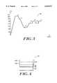
- FIG. 3is a graphical illustration of a multitemperature fabrication process for reducing threading dislocations
- FIG. 4shows a multilayer heteroepitaxial semiconductor structure fabricated in accord with the process of FIG. 3.
- the present inventionis particularly directed to heteroepitaxial semiconductor structures having a reduced density of dislocations.
- Dislocationsoccur at the interface between dissimilar semiconductor materials due primarily to differences in thermal coefficients of expansion and lattice mismatches. Even though the dislocations initiate at the interface between heteroepitaxial materials, they can thread through multiple subsequent homogeneous layers.
- FIG. 1shows a heteroepitaxial semiconductor structure 100 illustrative of the difficulties arising from threading dislocations.
- the structure 100includes a silicon (Si) substrate 102, a gallium arsenide (GaAs) nucleation layer 104 and a pair of epitaxial indium phosphide (InP) layers 106 and 108.
- the GaAs nucleation layer 104is employed as an intermediate layer between the Si substrate 102 and the epitaxial InP layer 104, because its lattice constant is intermediate between that of Si and InP.
- dislocationssuch as those shown at 110, nevertheless thread through the GaAs nucleation layer 104.
- dislocations 110Due to the additional lattice mismatch between GaAs and InP, a significant number of the dislocations 110 also thread through the InP epitaxial layer 106 into layer 108. As illustrated in layer 108, the dislocations 110 can continue to thread through additional homogeneous layers.
- the present inventionprovides an intermediate region between a substrate fabricated from one semiconductor material and a device fabricated from another semiconductor material on the substrate.
- An intermediate region according to the inventionimpedes the threading of dislocations from the substrate to any device fabricated thereon.
- FIG. 2depicts a heteroepitaxial semiconductor structure 200 having an intermediate region 204, which is fabricated between a substrate 202 and a semiconductor device 208 in accord with the present invention.
- the structure 200can include a nucleation layer 206 formed between the substrate 202 and the intermediate region 204.
- a tunnel junction 210 for facilitating electrical contact to the device 208can be formed between the device 208 and the intermediate region 204, or, in another embodiment of the invention, between a layer epitaxially grown on top of the nucleation layer 206 and the intermediate region 204.
- the substrate 202is Si.
- the semiconductor device 208is an InP photovoltaic cell. Since the device 208 is fabricated from InP, the intermediate region 204 is preferably also fabricated from InP. However, any suitable periodic table group III-V or II-VI material, which is substantially lattice matched to the material of device 208, can be employed. Additionally, other substrate materials, such as germanium (Ge) and GaAs can be used.
- the optional nucleation layer 206is preferably formed from GaAs. However, any semiconductor material having an intermediate lattice constant between the material of substrate 202 and the material of intermediate region 204 can be substituted in its place.
- dislocations 220can thread from the substrate 202 through the nucleation layer 206.
- the intermediate region 204is constructed to reduce the threading of the dislocations 220 to the device 208. More specifically, the intermediate region 204 of the depicted embodiment can be fabricated from a plurality of stacked groups 214-218 of InP layers. According to the illustrated embodiment, each stacked group 214-218 includes a first layer formed at a temperature in a first temperature range and a second layer formed at a temperature in a second temperature range.
- group 214has a first layer 214a and a second layer 214b; group 216 has a first layer 216a and a second layer 216b; and group 218 has a first layer 218a and a second layer 218b.
- Each of the layers 214a, 216a and 218aare formed at temperatures between about 575° C. and about 625° C.
- each of the layers 214b, 216b and 218bare formed at temperatures between about 650° C. and about 725° C.
- layers 214a, 216a and 218aare formed at substantially identical temperature
- layers 214b, 216b and 218bare formed at substantially identical temperature.
- adjacent layers of the stacked groups 214-218can be fabricated from different, but closely lattice matched materials.
- layers 214a and 214bcan be formed from semiconductor materials having a lattice mismatch of less than 1000 ppm.
- each group 214-218depicts each group 214-218 as being a pair of layers, other structures such as stacked triplets, quadruplets, quintuplets etc. can be employed. However, regardless of the structure of the stacked groups, a feature of the present invention is that adjacent layers in each group are formed at different temperatures.
- a further feature of the present inventionis that the temperature ranges in which the layers of each group are formed define a temperature profile, and the temperature profile repeats from group to group to form a thermally strained superlattice.
- stacked tripletscan be employed, wherein the temperatures at which the first, second and third layers of each triplet are formed are selected from first, second and third temperature ranges, respectively.
- the first and third layers of each tripletcan be formed at temperatures selected from a first temperature range, while the second layer of each triplet is formed at temperatures selected from a second temperature range.
- adjacent layers of each groupsuch as layers 214a and 214b, are formed to have different thicknesses, and the different thicknesses at which the layers of each group are formed define a thickness profile, which like the temperature profile discussed above, repeats from group to group.
- each epitaxial layer of InPhas a thickness of about 1 micron.
- the InP and GaAs layerscan be deposited by any epitaxial technique which provides high-quality semiconductor layers and p-n junctions.
- metalorganic chemical vapor depositionMOCVD
- MBEmolecular beam epitaxy
- LPEliquid-phase epitaxy
- the InP layers of groups 214-218are formed by MOCVD using a ratio of phosphorous to indium of approximately 200.
- the GaAs layer 206is formed from MOCVD using a gas ratio of arsenic to gallium of approximately 14.
- an InP photovoltaic cell 208is formed on the uppermost stacked group 218 of the intermediate region 204.
- the cell 208can have several epitaxial layers, formed as two groups 208a and 208b, each of a different doping type.
- One group of layers 208ais p-type doped and the other group 208b is n-type doped.
- group 208aconsists of two p-type InP layers 211a and 211b.
- the lower layer 211b(the back surface field of the solar cell) is doped with zinc to a concentration of about 3 ⁇ 10 18 cm -3 and is about a half micron thick.
- the upper layer 211a(the solar cell base) is doped with zinc to a concentration of about 1 ⁇ 10 17 cm -3 and is between about 3 microns and 5 microns thick.
- the lower layer 209b(the emitter of the solar cell) is doped with Si or selenium to a concentration of about 3 ⁇ 10 19 cm -3 , with a thickness of 0.1 microns or less.
- a tunnel junction 210is included to avoid the formation of a rectifying junction between the interface of the cell 208 and the intermediate region 204.
- the tunnel junction 210includes two semiconductor layers 210a and 210b, having opposite doping and being about one-half micron thick.
- tunnel junction layer 210ais n-type doped with Si or Se to a concentration of greater than about 10 19 cm -3 and tunnel junction layer 210b is p-type doped with Zn to a concentration of greater than about 10 19 cm -3 .
- the present inventioncan be used for fabrication of any heteroepitaxial semiconductor structures, an important motivation for its development arose generally from the field of photovoltaic cells (also called solar cells), and more specifically from the need for efficient photovoltaic cells for space applications.
- Photovoltaic cells for use in space applicationsrequire high power-to-weight ratios and strong resistance to radiation.
- InPhas generated considerable interest as a material for space photovoltaic cells, due to InP's inherent radiation resistance.
- InP cells fabricated on InP substratessuffer from two drawbacks in comparison with cells fabricated on Si substrates.
- the InP substrate costis much higher and the physical fragility of InP requires a greater substrate thickness in order to make fabrication practical. The greater thickness results in increased mass and therefore, a lower power-to-weight ratio.
- Silicon substratesare much less expensive than InP substrates and are available in larger sizes. Additionally, the greater mechanical strength (which allows a thinner substrate wafer) and lower density of Si reduce cell mass, and increase the power-to-weight-ratio.
- EOL efficiencyis the figure used by aerospace designers. EOL efficiency is the value to which the efficiency is expected to degrade, after exposure to the amount of radiation calculated for the life of the mission in a particular orbit.
- InP photovoltaic cells fabricated on InP substrateshave a longer carrier lifetime and higher beginning-of-life (BOL) efficiency (before any irradiation, at the start of the space mission) than do InP cells fabricated on Si substrates, since the process of making the InP cells on Si wafers results in certain intrinsic defects, due the lattice constant and thermal expansion coefficient mismatch discussed previously.
- BOL efficiency for an InP cell on an InP substratecan be over 19%, while BOL efficiency for an InP cell on a Si substrate is about 13%.
- the power conversion efficiency of InP cell on InP substratesinitially degrades faster than does the efficiency of InP cells on Si wafers during early exposure to radiation.
- the EOL efficienciestend to become similar for the two architectures, in one particular case about 10% for cells on both types of substrates.
- This similarity in efficiency between the InP cells on the two types of substratesis due to the fact that the radiation exposure and damage to both cells is similar, and that the degradation due to the radiation damage exceeds the degradation due to the defects in the InP cell on Si substrate that resulted from the mismatches in lattice constant and thermal expansion coefficients discussed previously.
- the InP cell on Si substrateprovides a similar amount of EOL power compared to the InP cell on InP substrate, with an improved EOL power-to-weight ratio since the Si substrate wafer is only half as dense than the InP substrate, and, in addition, the Si substrate can be thinner since it is less fragile.
- dislocations that thread from the Si substrate to the InP cellcan be substantially reduced.
- InP cells on Si substratescan be fabricated to have BOL efficiencies that approach the high BOL efficiencies of InP cells on InP wafers.
- the EOL efficiency for lower radiation orbits, such as the low earth orbits (LEO) and geosynchronous earth orbits (GEO) popular with many communication satelliteswill benefit from this improvement.
- Dislocation reducing methods for heteroepitaxial structuresenable InP cells on Si substrates to compete effectively with other standard solar cells in lower radiation orbits, in addition to the higher radiation orbits in which InP cells on Si substrates now show the greatest advantage.
- the inventionfurther reduces threading dislocations through a further temperature cycled process in which a very thin arsenic layer is formed to aid in the nucleation of the epilayers.
- FIG. 3is a graphical representation 300 of such a further process according to the invention.
- FIG. 4shows a heteroepitaxial structure 400 formed from the process of FIG. 3. Referring to FIGS. 3 and 4, a substrate 402 formed from a first semiconductor material, preferably Si, is heated to a first temperature T1 in excess of about 1000° C. Optionally, a prenucleation layer 404 of arsenic is then formed on the Si substrate 402 at a second temperature T2 in the range of about 800° C. to about 840° C.
- the arsenic prenucleation layer 404is less than about a few monolayers thick (i.e., approximately 5-10 angstroms).
- a nucleation layer 406similar in structure to nucleation layer 206 and preferably constructed from GaAs, is formed on the prenucleation layer 404.
- the GaAs nucleation layer 406is amorphous and is fabricated at a temperature T3 in the range of about 350° C. and about 450° C.
- the nucleation layer 406is preferably less than 200 angstroms thick. It can be formed from MOCVD with an arsenic to gallium gas ratio of 14.
- the nucleation layer 406can be formed directly on the substrate 402 and the prenucleation layer 404 can be omitted.
- an intermediate region 408similar in construction to the intermediate region 204 of FIG. 2, can be fabricated thereon.
- the intermediate regioncomprises one or more pairs of epitaxial layers of n-doped InP.
- Each pairincludes a first layer 408a fabricated at a fourth temperature T4 in a range of about 575° C. to about 625° C. and a second layer 408b fabricated at a fifth temperature T5 in a range of about 650° C. to about 725° C.
Landscapes
- Engineering & Computer Science (AREA)
- Physics & Mathematics (AREA)
- Condensed Matter Physics & Semiconductors (AREA)
- General Physics & Mathematics (AREA)
- Manufacturing & Machinery (AREA)
- Computer Hardware Design (AREA)
- Microelectronics & Electronic Packaging (AREA)
- Power Engineering (AREA)
- Chemical & Material Sciences (AREA)
- Materials Engineering (AREA)
- Recrystallisation Techniques (AREA)
Abstract
Description
Claims (36)
Priority Applications (2)
| Application Number | Priority Date | Filing Date | Title |
|---|---|---|---|
| US08/523,694US6010937A (en) | 1995-09-05 | 1995-09-05 | Reduction of dislocations in a heteroepitaxial semiconductor structure |
| PCT/US1996/014051WO1997009738A1 (en) | 1995-09-05 | 1996-09-03 | Reduction of dislocations in a heteroepitaxial semiconductor structure |
Applications Claiming Priority (1)
| Application Number | Priority Date | Filing Date | Title |
|---|---|---|---|
| US08/523,694US6010937A (en) | 1995-09-05 | 1995-09-05 | Reduction of dislocations in a heteroepitaxial semiconductor structure |
Publications (1)
| Publication Number | Publication Date |
|---|---|
| US6010937Atrue US6010937A (en) | 2000-01-04 |
Family
ID=24086049
Family Applications (1)
| Application Number | Title | Priority Date | Filing Date |
|---|---|---|---|
| US08/523,694Expired - LifetimeUS6010937A (en) | 1995-09-05 | 1995-09-05 | Reduction of dislocations in a heteroepitaxial semiconductor structure |
Country Status (2)
| Country | Link |
|---|---|
| US (1) | US6010937A (en) |
| WO (1) | WO1997009738A1 (en) |
Cited By (244)
| Publication number | Priority date | Publication date | Assignee | Title |
|---|---|---|---|---|
| US6503773B2 (en)* | 2000-01-20 | 2003-01-07 | Amberwave Systems Corporation | Low threading dislocation density relaxed mismatched epilayers without high temperature growth |
| US6555846B1 (en)* | 1999-06-10 | 2003-04-29 | Pioneer Corporation | Method for manufacturing a nitride semiconductor device and device manufactured by the method |
| US6589335B2 (en)* | 2001-02-08 | 2003-07-08 | Amberwave Systems Corporation | Relaxed InxGa1-xAs layers integrated with Si |
| US20040040493A1 (en)* | 2002-08-30 | 2004-03-04 | Amberwave Systems Corporation | Reduction of dislocation pile-up formation during relaxed lattice-mismatched epitaxy |
| US20040075105A1 (en)* | 2002-08-23 | 2004-04-22 | Amberwave Systems Corporation | Semiconductor heterostructures having reduced dislocation pile-ups and related methods |
| US20040161013A1 (en)* | 2003-02-13 | 2004-08-19 | David Bour | Laser employing a zinc-doped tunnel-junction |
| US20040262631A1 (en)* | 1997-06-24 | 2004-12-30 | Massachusetts Institute Of Technology | Controlling threading dislocation densities in Ge on Si using graded GeSi layers and planarization |
| US6855959B2 (en)* | 2000-03-24 | 2005-02-15 | Nec Corporation | Nitride based semiconductor photo-luminescent device |
| US7332417B2 (en) | 2003-01-27 | 2008-02-19 | Amberwave Systems Corporation | Semiconductor structures with structural homogeneity |
| US20130220407A1 (en)* | 2012-02-29 | 2013-08-29 | The Boeing Company | Solar Cell with Delta Doping Layer |
| US20160141391A1 (en)* | 2014-11-13 | 2016-05-19 | Imec Vzw | Method for Reducing Contact Resistance in MOS |
| US9711683B2 (en)* | 2014-09-26 | 2017-07-18 | Epistar Corporation | Semiconductor device and the method of manufacturing the same |
| US10159412B2 (en) | 2010-12-01 | 2018-12-25 | Cercacor Laboratories, Inc. | Handheld processing device including medical applications for minimally and non invasive glucose measurements |
| US10615177B2 (en)* | 2015-09-04 | 2020-04-07 | Stmicroelectronics, Inc. | Method for manufacturing a transistor having a sharp junction by forming raised source-drain regions before forming gate regions and corresponding transistor produced by said method |
| US10736518B2 (en) | 2015-08-31 | 2020-08-11 | Masimo Corporation | Systems and methods to monitor repositioning of a patient |
| US10765367B2 (en) | 2014-10-07 | 2020-09-08 | Masimo Corporation | Modular physiological sensors |
| US10779098B2 (en) | 2018-07-10 | 2020-09-15 | Masimo Corporation | Patient monitor alarm speaker analyzer |
| US10784634B2 (en) | 2015-02-06 | 2020-09-22 | Masimo Corporation | Pogo pin connector |
| USD897098S1 (en) | 2018-10-12 | 2020-09-29 | Masimo Corporation | Card holder set |
| US10799163B2 (en) | 2006-10-12 | 2020-10-13 | Masimo Corporation | Perfusion index smoother |
| US10799160B2 (en) | 2013-10-07 | 2020-10-13 | Masimo Corporation | Regional oximetry pod |
| US10825568B2 (en) | 2013-10-11 | 2020-11-03 | Masimo Corporation | Alarm notification system |
| US10849554B2 (en) | 2017-04-18 | 2020-12-01 | Masimo Corporation | Nose sensor |
| US10856750B2 (en) | 2017-04-28 | 2020-12-08 | Masimo Corporation | Spot check measurement system |
| US10856788B2 (en) | 2005-03-01 | 2020-12-08 | Cercacor Laboratories, Inc. | Noninvasive multi-parameter patient monitor |
| US10863938B2 (en) | 2006-10-12 | 2020-12-15 | Masimo Corporation | System and method for monitoring the life of a physiological sensor |
| US10869602B2 (en) | 2002-03-25 | 2020-12-22 | Masimo Corporation | Physiological measurement communications adapter |
| US10912500B2 (en) | 2008-07-03 | 2021-02-09 | Masimo Corporation | Multi-stream data collection system for noninvasive measurement of blood constituents |
| US10912524B2 (en) | 2006-09-22 | 2021-02-09 | Masimo Corporation | Modular patient monitor |
| US10918281B2 (en) | 2017-04-26 | 2021-02-16 | Masimo Corporation | Medical monitoring device having multiple configurations |
| US10925550B2 (en) | 2011-10-13 | 2021-02-23 | Masimo Corporation | Medical monitoring hub |
| US10932705B2 (en) | 2017-05-08 | 2021-03-02 | Masimo Corporation | System for displaying and controlling medical monitoring data |
| US10932729B2 (en) | 2018-06-06 | 2021-03-02 | Masimo Corporation | Opioid overdose monitoring |
| US10939877B2 (en) | 2005-10-14 | 2021-03-09 | Masimo Corporation | Robust alarm system |
| US10943450B2 (en) | 2009-12-21 | 2021-03-09 | Masimo Corporation | Modular patient monitor |
| US10952641B2 (en) | 2008-09-15 | 2021-03-23 | Masimo Corporation | Gas sampling line |
| US10956950B2 (en) | 2017-02-24 | 2021-03-23 | Masimo Corporation | Managing dynamic licenses for physiological parameters in a patient monitoring environment |
| US10959652B2 (en) | 2001-07-02 | 2021-03-30 | Masimo Corporation | Low power pulse oximeter |
| USD916135S1 (en) | 2018-10-11 | 2021-04-13 | Masimo Corporation | Display screen or portion thereof with a graphical user interface |
| US10973447B2 (en) | 2003-01-24 | 2021-04-13 | Masimo Corporation | Noninvasive oximetry optical sensor including disposable and reusable elements |
| US10980432B2 (en) | 2013-08-05 | 2021-04-20 | Masimo Corporation | Systems and methods for measuring blood pressure |
| US10980457B2 (en) | 2007-04-21 | 2021-04-20 | Masimo Corporation | Tissue profile wellness monitor |
| USD917704S1 (en) | 2019-08-16 | 2021-04-27 | Masimo Corporation | Patient monitor |
| USD917564S1 (en) | 2018-10-11 | 2021-04-27 | Masimo Corporation | Display screen or portion thereof with graphical user interface |
| US10991135B2 (en) | 2015-08-11 | 2021-04-27 | Masimo Corporation | Medical monitoring analysis and replay including indicia responsive to light attenuated by body tissue |
| USD917550S1 (en) | 2018-10-11 | 2021-04-27 | Masimo Corporation | Display screen or portion thereof with a graphical user interface |
| US10987066B2 (en) | 2017-10-31 | 2021-04-27 | Masimo Corporation | System for displaying oxygen state indications |
| US10993643B2 (en) | 2006-10-12 | 2021-05-04 | Masimo Corporation | Patient monitor capable of monitoring the quality of attached probes and accessories |
| US10993662B2 (en) | 2016-03-04 | 2021-05-04 | Masimo Corporation | Nose sensor |
| USD919094S1 (en) | 2019-08-16 | 2021-05-11 | Masimo Corporation | Blood pressure device |
| US11000232B2 (en) | 2014-06-19 | 2021-05-11 | Masimo Corporation | Proximity sensor in pulse oximeter |
| USD919100S1 (en) | 2019-08-16 | 2021-05-11 | Masimo Corporation | Holder for a patient monitor |
| US11020084B2 (en) | 2012-09-20 | 2021-06-01 | Masimo Corporation | Acoustic patient sensor coupler |
| US11022466B2 (en) | 2013-07-17 | 2021-06-01 | Masimo Corporation | Pulser with double-bearing position encoder for non-invasive physiological monitoring |
| USD921202S1 (en) | 2019-08-16 | 2021-06-01 | Masimo Corporation | Holder for a blood pressure device |
| US11020029B2 (en) | 2003-07-25 | 2021-06-01 | Masimo Corporation | Multipurpose sensor port |
| US11026604B2 (en) | 2017-07-13 | 2021-06-08 | Cercacor Laboratories, Inc. | Medical monitoring device for harmonizing physiological measurements |
| US11033210B2 (en) | 2008-03-04 | 2021-06-15 | Masimo Corporation | Multispot monitoring for use in optical coherence tomography |
| USD925597S1 (en) | 2017-10-31 | 2021-07-20 | Masimo Corporation | Display screen or portion thereof with graphical user interface |
| US11069461B2 (en) | 2012-08-01 | 2021-07-20 | Masimo Corporation | Automated assembly sensor cable |
| US11071480B2 (en) | 2012-04-17 | 2021-07-27 | Masimo Corporation | Hypersaturation index |
| US11076777B2 (en) | 2016-10-13 | 2021-08-03 | Masimo Corporation | Systems and methods for monitoring orientation to reduce pressure ulcer formation |
| US11087875B2 (en) | 2009-03-04 | 2021-08-10 | Masimo Corporation | Medical monitoring system |
| US11086609B2 (en) | 2017-02-24 | 2021-08-10 | Masimo Corporation | Medical monitoring hub |
| USD927699S1 (en) | 2019-10-18 | 2021-08-10 | Masimo Corporation | Electrode pad |
| US11083397B2 (en) | 2012-02-09 | 2021-08-10 | Masimo Corporation | Wireless patient monitoring device |
| US11095068B2 (en) | 2017-08-15 | 2021-08-17 | Masimo Corporation | Water resistant connector for noninvasive patient monitor |
| US11089982B2 (en) | 2011-10-13 | 2021-08-17 | Masimo Corporation | Robust fractional saturation determination |
| US11096631B2 (en) | 2017-02-24 | 2021-08-24 | Masimo Corporation | Modular multi-parameter patient monitoring device |
| US11103134B2 (en) | 2014-09-18 | 2021-08-31 | Masimo Semiconductor, Inc. | Enhanced visible near-infrared photodiode and non-invasive physiological sensor |
| US11109770B2 (en) | 2011-06-21 | 2021-09-07 | Masimo Corporation | Patient monitoring system |
| US11114188B2 (en) | 2009-10-06 | 2021-09-07 | Cercacor Laboratories, Inc. | System for monitoring a physiological parameter of a user |
| US11109818B2 (en) | 2018-04-19 | 2021-09-07 | Masimo Corporation | Mobile patient alarm display |
| US11132117B2 (en) | 2012-03-25 | 2021-09-28 | Masimo Corporation | Physiological monitor touchscreen interface |
| US11133105B2 (en) | 2009-03-04 | 2021-09-28 | Masimo Corporation | Medical monitoring system |
| USD933232S1 (en) | 2020-05-11 | 2021-10-12 | Masimo Corporation | Blood pressure monitor |
| US11145408B2 (en) | 2009-03-04 | 2021-10-12 | Masimo Corporation | Medical communication protocol translator |
| US11147518B1 (en) | 2013-10-07 | 2021-10-19 | Masimo Corporation | Regional oximetry signal processor |
| US11153089B2 (en) | 2016-07-06 | 2021-10-19 | Masimo Corporation | Secure and zero knowledge data sharing for cloud applications |
| US11172890B2 (en) | 2012-01-04 | 2021-11-16 | Masimo Corporation | Automated condition screening and detection |
| US11176801B2 (en) | 2011-08-19 | 2021-11-16 | Masimo Corporation | Health care sanitation monitoring system |
| US11178776B2 (en) | 2015-02-06 | 2021-11-16 | Masimo Corporation | Fold flex circuit for LNOP |
| US11179111B2 (en) | 2012-01-04 | 2021-11-23 | Masimo Corporation | Automated CCHD screening and detection |
| US11185262B2 (en) | 2017-03-10 | 2021-11-30 | Masimo Corporation | Pneumonia screener |
| US11191485B2 (en) | 2006-06-05 | 2021-12-07 | Masimo Corporation | Parameter upgrade system |
| US11191484B2 (en) | 2016-04-29 | 2021-12-07 | Masimo Corporation | Optical sensor tape |
| US11202571B2 (en) | 2016-07-07 | 2021-12-21 | Masimo Corporation | Wearable pulse oximeter and respiration monitor |
| US11224363B2 (en) | 2013-01-16 | 2022-01-18 | Masimo Corporation | Active-pulse blood analysis system |
| US11229374B2 (en) | 2006-12-09 | 2022-01-25 | Masimo Corporation | Plethysmograph variability processor |
| US11234655B2 (en) | 2007-01-20 | 2022-02-01 | Masimo Corporation | Perfusion trend indicator |
| US11241199B2 (en) | 2011-10-13 | 2022-02-08 | Masimo Corporation | System for displaying medical monitoring data |
| US11259745B2 (en) | 2014-01-28 | 2022-03-01 | Masimo Corporation | Autonomous drug delivery system |
| US11272852B2 (en) | 2011-06-21 | 2022-03-15 | Masimo Corporation | Patient monitoring system |
| US11272839B2 (en) | 2018-10-12 | 2022-03-15 | Ma Simo Corporation | System for transmission of sensor data using dual communication protocol |
| US11272883B2 (en) | 2016-03-04 | 2022-03-15 | Masimo Corporation | Physiological sensor |
| US11289199B2 (en) | 2010-01-19 | 2022-03-29 | Masimo Corporation | Wellness analysis system |
| US11291061B2 (en) | 2017-01-18 | 2022-03-29 | Masimo Corporation | Patient-worn wireless physiological sensor with pairing functionality |
| USRE49007E1 (en) | 2010-03-01 | 2022-04-05 | Masimo Corporation | Adaptive alarm system |
| US11291415B2 (en) | 2015-05-04 | 2022-04-05 | Cercacor Laboratories, Inc. | Noninvasive sensor system with visual infographic display |
| US11298021B2 (en) | 2017-10-19 | 2022-04-12 | Masimo Corporation | Medical monitoring system |
| USRE49034E1 (en) | 2002-01-24 | 2022-04-19 | Masimo Corporation | Physiological trend monitor |
| US11331013B2 (en) | 2014-09-04 | 2022-05-17 | Masimo Corporation | Total hemoglobin screening sensor |
| US11330996B2 (en) | 2010-05-06 | 2022-05-17 | Masimo Corporation | Patient monitor for determining microcirculation state |
| US11363960B2 (en) | 2011-02-25 | 2022-06-21 | Masimo Corporation | Patient monitor for monitoring microcirculation |
| US11367529B2 (en) | 2012-11-05 | 2022-06-21 | Cercacor Laboratories, Inc. | Physiological test credit method |
| US11389093B2 (en) | 2018-10-11 | 2022-07-19 | Masimo Corporation | Low noise oximetry cable |
| US11399722B2 (en) | 2010-03-30 | 2022-08-02 | Masimo Corporation | Plethysmographic respiration rate detection |
| US11399774B2 (en) | 2010-10-13 | 2022-08-02 | Masimo Corporation | Physiological measurement logic engine |
| US11410507B2 (en) | 2017-02-24 | 2022-08-09 | Masimo Corporation | Localized projection of audible noises in medical settings |
| US11406286B2 (en) | 2018-10-11 | 2022-08-09 | Masimo Corporation | Patient monitoring device with improved user interface |
| US11417426B2 (en) | 2017-02-24 | 2022-08-16 | Masimo Corporation | System for displaying medical monitoring data |
| US11412964B2 (en) | 2008-05-05 | 2022-08-16 | Masimo Corporation | Pulse oximetry system with electrical decoupling circuitry |
| US11426104B2 (en) | 2004-08-11 | 2022-08-30 | Masimo Corporation | Method for data reduction and calibration of an OCT-based physiological monitor |
| US11426125B2 (en) | 2009-02-16 | 2022-08-30 | Masimo Corporation | Physiological measurement device |
| US11439329B2 (en) | 2011-07-13 | 2022-09-13 | Masimo Corporation | Multiple measurement mode in a physiological sensor |
| US11445948B2 (en) | 2018-10-11 | 2022-09-20 | Masimo Corporation | Patient connector assembly with vertical detents |
| US11452449B2 (en) | 2012-10-30 | 2022-09-27 | Masimo Corporation | Universal medical system |
| US11464410B2 (en) | 2018-10-12 | 2022-10-11 | Masimo Corporation | Medical systems and methods |
| US11484231B2 (en) | 2010-03-08 | 2022-11-01 | Masimo Corporation | Reprocessing of a physiological sensor |
| US11488715B2 (en) | 2011-02-13 | 2022-11-01 | Masimo Corporation | Medical characterization system |
| US11504066B1 (en) | 2015-09-04 | 2022-11-22 | Cercacor Laboratories, Inc. | Low-noise sensor system |
| US11504002B2 (en) | 2012-09-20 | 2022-11-22 | Masimo Corporation | Physiological monitoring system |
| US11504062B2 (en) | 2013-03-14 | 2022-11-22 | Masimo Corporation | Patient monitor placement indicator |
| US11504058B1 (en) | 2016-12-02 | 2022-11-22 | Masimo Corporation | Multi-site noninvasive measurement of a physiological parameter |
| US11515664B2 (en) | 2009-03-11 | 2022-11-29 | Masimo Corporation | Magnetic connector |
| USD973072S1 (en) | 2020-09-30 | 2022-12-20 | Masimo Corporation | Display screen or portion thereof with graphical user interface |
| US11534087B2 (en) | 2009-11-24 | 2022-12-27 | Cercacor Laboratories, Inc. | Physiological measurement system with automatic wavelength adjustment |
| USD973686S1 (en) | 2020-09-30 | 2022-12-27 | Masimo Corporation | Display screen or portion thereof with graphical user interface |
| USD973685S1 (en) | 2020-09-30 | 2022-12-27 | Masimo Corporation | Display screen or portion thereof with graphical user interface |
| USD974193S1 (en) | 2020-07-27 | 2023-01-03 | Masimo Corporation | Wearable temperature measurement device |
| US11559275B2 (en) | 2008-12-30 | 2023-01-24 | Masimo Corporation | Acoustic sensor assembly |
| US11571152B2 (en) | 2009-12-04 | 2023-02-07 | Masimo Corporation | Calibration for multi-stage physiological monitors |
| US11581091B2 (en) | 2014-08-26 | 2023-02-14 | Vccb Holdings, Inc. | Real-time monitoring systems and methods in a healthcare environment |
| USD979516S1 (en) | 2020-05-11 | 2023-02-28 | Masimo Corporation | Connector |
| US11596363B2 (en) | 2013-09-12 | 2023-03-07 | Cercacor Laboratories, Inc. | Medical device management system |
| USD980091S1 (en) | 2020-07-27 | 2023-03-07 | Masimo Corporation | Wearable temperature measurement device |
| US11602289B2 (en) | 2015-02-06 | 2023-03-14 | Masimo Corporation | Soft boot pulse oximetry sensor |
| US11607139B2 (en) | 2006-09-20 | 2023-03-21 | Masimo Corporation | Congenital heart disease monitor |
| US11622733B2 (en) | 2008-05-02 | 2023-04-11 | Masimo Corporation | Monitor configuration system |
| US11637437B2 (en) | 2019-04-17 | 2023-04-25 | Masimo Corporation | Charging station for physiological monitoring device |
| US11638532B2 (en) | 2008-07-03 | 2023-05-02 | Masimo Corporation | User-worn device for noninvasively measuring a physiological parameter of a user |
| USD985498S1 (en) | 2019-08-16 | 2023-05-09 | Masimo Corporation | Connector |
| US11645905B2 (en) | 2013-03-13 | 2023-05-09 | Masimo Corporation | Systems and methods for monitoring a patient health network |
| US11653862B2 (en) | 2015-05-22 | 2023-05-23 | Cercacor Laboratories, Inc. | Non-invasive optical physiological differential pathlength sensor |
| US11672447B2 (en) | 2006-10-12 | 2023-06-13 | Masimo Corporation | Method and apparatus for calibration to reduce coupling between signals in a measurement system |
| US11673041B2 (en) | 2013-12-13 | 2023-06-13 | Masimo Corporation | Avatar-incentive healthcare therapy |
| US11679579B2 (en) | 2015-12-17 | 2023-06-20 | Masimo Corporation | Varnish-coated release liner |
| US11684296B2 (en) | 2018-12-21 | 2023-06-27 | Cercacor Laboratories, Inc. | Noninvasive physiological sensor |
| US11690574B2 (en) | 2003-11-05 | 2023-07-04 | Masimo Corporation | Pulse oximeter access apparatus and method |
| US11696712B2 (en) | 2014-06-13 | 2023-07-11 | Vccb Holdings, Inc. | Alarm fatigue management systems and methods |
| US11717210B2 (en) | 2010-09-28 | 2023-08-08 | Masimo Corporation | Depth of consciousness monitor including oximeter |
| US11721105B2 (en) | 2020-02-13 | 2023-08-08 | Masimo Corporation | System and method for monitoring clinical activities |
| US11724031B2 (en) | 2006-01-17 | 2023-08-15 | Masimo Corporation | Drug administration controller |
| US11730379B2 (en) | 2020-03-20 | 2023-08-22 | Masimo Corporation | Remote patient management and monitoring systems and methods |
| USD997365S1 (en) | 2021-06-24 | 2023-08-29 | Masimo Corporation | Physiological nose sensor |
| US11747178B2 (en) | 2011-10-27 | 2023-09-05 | Masimo Corporation | Physiological monitor gauge panel |
| US11744471B2 (en) | 2009-09-17 | 2023-09-05 | Masimo Corporation | Optical-based physiological monitoring system |
| USD998630S1 (en) | 2018-10-11 | 2023-09-12 | Masimo Corporation | Display screen or portion thereof with a graphical user interface |
| USD998631S1 (en) | 2018-10-11 | 2023-09-12 | Masimo Corporation | Display screen or portion thereof with a graphical user interface |
| US11752262B2 (en) | 2009-05-20 | 2023-09-12 | Masimo Corporation | Hemoglobin display and patient treatment |
| USD999246S1 (en) | 2018-10-11 | 2023-09-19 | Masimo Corporation | Display screen or portion thereof with a graphical user interface |
| US11766198B2 (en) | 2018-02-02 | 2023-09-26 | Cercacor Laboratories, Inc. | Limb-worn patient monitoring device |
| USD1000975S1 (en) | 2021-09-22 | 2023-10-10 | Masimo Corporation | Wearable temperature measurement device |
| US11779247B2 (en) | 2009-07-29 | 2023-10-10 | Masimo Corporation | Non-invasive physiological sensor cover |
| US11803623B2 (en) | 2019-10-18 | 2023-10-31 | Masimo Corporation | Display layout and interactive objects for patient monitoring |
| US11816771B2 (en) | 2017-02-24 | 2023-11-14 | Masimo Corporation | Augmented reality system for displaying patient data |
| US11832940B2 (en) | 2019-08-27 | 2023-12-05 | Cercacor Laboratories, Inc. | Non-invasive medical monitoring device for blood analyte measurements |
| US11864890B2 (en) | 2016-12-22 | 2024-01-09 | Cercacor Laboratories, Inc. | Methods and devices for detecting intensity of light with translucent detector |
| US11872156B2 (en) | 2018-08-22 | 2024-01-16 | Masimo Corporation | Core body temperature measurement |
| US11879960B2 (en) | 2020-02-13 | 2024-01-23 | Masimo Corporation | System and method for monitoring clinical activities |
| US11877824B2 (en) | 2011-08-17 | 2024-01-23 | Masimo Corporation | Modulated physiological sensor |
| US11887728B2 (en) | 2012-09-20 | 2024-01-30 | Masimo Corporation | Intelligent medical escalation process |
| US11883129B2 (en) | 2018-04-24 | 2024-01-30 | Cercacor Laboratories, Inc. | Easy insert finger sensor for transmission based spectroscopy sensor |
| US11937949B2 (en) | 2004-03-08 | 2024-03-26 | Masimo Corporation | Physiological parameter system |
| US11944431B2 (en) | 2006-03-17 | 2024-04-02 | Masimo Corportation | Apparatus and method for creating a stable optical interface |
| US11951186B2 (en) | 2019-10-25 | 2024-04-09 | Willow Laboratories, Inc. | Indicator compounds, devices comprising indicator compounds, and methods of making and using the same |
| US11963736B2 (en) | 2009-07-20 | 2024-04-23 | Masimo Corporation | Wireless patient monitoring system |
| US11963749B2 (en) | 2013-03-13 | 2024-04-23 | Masimo Corporation | Acoustic physiological monitoring system |
| US11974841B2 (en) | 2009-10-16 | 2024-05-07 | Masimo Corporation | Respiration processor |
| US11986289B2 (en) | 2018-11-27 | 2024-05-21 | Willow Laboratories, Inc. | Assembly for medical monitoring device with multiple physiological sensors |
| US11990706B2 (en) | 2012-02-08 | 2024-05-21 | Masimo Corporation | Cable tether system |
| US11986067B2 (en) | 2020-08-19 | 2024-05-21 | Masimo Corporation | Strap for a wearable device |
| US11992342B2 (en) | 2013-01-02 | 2024-05-28 | Masimo Corporation | Acoustic respiratory monitoring sensor with probe-off detection |
| US11998362B2 (en) | 2009-10-15 | 2024-06-04 | Masimo Corporation | Acoustic respiratory monitoring sensor having multiple sensing elements |
| US12004881B2 (en) | 2012-01-04 | 2024-06-11 | Masimo Corporation | Automated condition screening and detection |
| US12004869B2 (en) | 2018-11-05 | 2024-06-11 | Masimo Corporation | System to monitor and manage patient hydration via plethysmograph variablity index in response to the passive leg raising |
| US12014328B2 (en) | 2005-07-13 | 2024-06-18 | Vccb Holdings, Inc. | Medicine bottle cap with electronic embedded curved display |
| USD1031729S1 (en) | 2017-08-15 | 2024-06-18 | Masimo Corporation | Connector |
| US12016721B2 (en) | 2013-10-11 | 2024-06-25 | Masimo Corporation | Acoustic sensor with attachment portion |
| US12016661B2 (en) | 2011-01-10 | 2024-06-25 | Masimo Corporation | Non-invasive intravascular volume index monitor |
| US12029586B2 (en) | 2006-10-12 | 2024-07-09 | Masimo Corporation | Oximeter probe off indicator defining probe off space |
| US12029844B2 (en) | 2020-06-25 | 2024-07-09 | Willow Laboratories, Inc. | Combination spirometer-inhaler |
| US12036014B2 (en) | 2015-01-23 | 2024-07-16 | Masimo Corporation | Nasal/oral cannula system and manufacturing |
| US12042285B1 (en) | 2012-08-29 | 2024-07-23 | Masimo Corporation | Physiological measurement calibration |
| USD1036293S1 (en) | 2021-08-17 | 2024-07-23 | Masimo Corporation | Straps for a wearable device |
| US12048534B2 (en) | 2020-03-04 | 2024-07-30 | Willow Laboratories, Inc. | Systems and methods for securing a tissue site to a sensor |
| US12066426B1 (en) | 2019-01-16 | 2024-08-20 | Masimo Corporation | Pulsed micro-chip laser for malaria detection |
| US12076159B2 (en) | 2019-02-07 | 2024-09-03 | Masimo Corporation | Combining multiple QEEG features to estimate drug-independent sedation level using machine learning |
| US12082926B2 (en) | 2020-08-04 | 2024-09-10 | Masimo Corporation | Optical sensor with multiple detectors or multiple emitters |
| USD1041511S1 (en) | 2018-10-11 | 2024-09-10 | Masimo Corporation | Display screen or portion thereof with a graphical user interface |
| USD1042596S1 (en) | 2022-12-12 | 2024-09-17 | Masimo Corporation | Monitoring camera |
| US12089968B2 (en) | 2006-12-22 | 2024-09-17 | Masimo Corporation | Optical patient monitor |
| US12097043B2 (en) | 2018-06-06 | 2024-09-24 | Masimo Corporation | Locating a locally stored medication |
| US12114974B2 (en) | 2020-01-13 | 2024-10-15 | Masimo Corporation | Wearable device with physiological parameters monitoring |
| USD1048571S1 (en) | 2021-10-07 | 2024-10-22 | Masimo Corporation | Bite block |
| US12126683B2 (en) | 2021-08-31 | 2024-10-22 | Masimo Corporation | Privacy switch for mobile communications device |
| US12131661B2 (en) | 2019-10-03 | 2024-10-29 | Willow Laboratories, Inc. | Personalized health coaching system |
| US12128213B2 (en) | 2020-01-30 | 2024-10-29 | Willow Laboratories, Inc. | Method of operating redundant staggered disease management systems |
| USD1048908S1 (en) | 2022-10-04 | 2024-10-29 | Masimo Corporation | Wearable sensor |
| US12127838B2 (en) | 2020-04-22 | 2024-10-29 | Willow Laboratories, Inc. | Self-contained minimal action invasive blood constituent system |
| US12138079B2 (en) | 2016-11-30 | 2024-11-12 | Masimo Corporation | Haemodynamic monitor with improved filtering |
| US12178572B1 (en) | 2013-06-11 | 2024-12-31 | Masimo Corporation | Blood glucose sensing system |
| US12178852B2 (en) | 2020-09-30 | 2024-12-31 | Willow Laboratories, Inc. | Insulin formulations and uses in infusion devices |
| USD1057159S1 (en) | 2022-03-29 | 2025-01-07 | Masimo Corporation | Electronic measurement device |
| USD1057160S1 (en) | 2022-03-29 | 2025-01-07 | Masimo Corporation | Electronic measurement device |
| US12198790B1 (en) | 2010-10-07 | 2025-01-14 | Masimo Corporation | Physiological monitor sensor systems and methods |
| US12201702B1 (en) | 2016-02-12 | 2025-01-21 | Masimo Corporation | Diagnosis, removal, or mechanical damaging of tumor using plasmonic nanobubbles |
| US12207901B1 (en) | 2019-08-16 | 2025-01-28 | Masimo Corporation | Optical detection of transient vapor nanobubbles in a microfluidic device |
| USD1061585S1 (en) | 2020-10-16 | 2025-02-11 | Masimo Corporation | Display screen or portion thereof with graphical user interface |
| US12220207B2 (en) | 2019-02-26 | 2025-02-11 | Masimo Corporation | Non-contact core body temperature measurement systems and methods |
| USD1063893S1 (en) | 2022-03-11 | 2025-02-25 | Masimo Corporation | Electronic device |
| US12236767B2 (en) | 2022-01-11 | 2025-02-25 | Masimo Corporation | Machine learning based monitoring system |
| USD1066244S1 (en) | 2023-05-11 | 2025-03-11 | Masimo Corporation | Charger |
| US12257081B2 (en) | 2009-10-15 | 2025-03-25 | Masimo Corporation | Bidirectional physiological information display |
| USD1068656S1 (en) | 2023-05-11 | 2025-04-01 | Masimo Corporation | Charger |
| US12272445B1 (en) | 2019-12-05 | 2025-04-08 | Masimo Corporation | Automated medical coding |
| USD1071195S1 (en) | 2022-10-06 | 2025-04-15 | Masimo Corporation | Mounting device for a medical transducer |
| USD1072837S1 (en) | 2020-10-27 | 2025-04-29 | Masimo Corporation | Display screen or portion thereof with graphical user interface |
| USD1072836S1 (en) | 2020-10-16 | 2025-04-29 | Masimo Corporation | Display screen or portion thereof with graphical user interface |
| USD1078689S1 (en) | 2022-12-12 | 2025-06-10 | Masimo Corporation | Electronic device |
| US12336796B2 (en) | 2021-07-13 | 2025-06-24 | Masimo Corporation | Wearable device with physiological parameters monitoring |
| US12343108B2 (en) | 2013-03-15 | 2025-07-01 | Willow Laboratories, Inc. | Cloud-based physiological monitoring system |
| US12362596B2 (en) | 2021-08-19 | 2025-07-15 | Masimo Corporation | Wearable physiological monitoring devices |
| USD1083653S1 (en) | 2022-09-09 | 2025-07-15 | Masimo Corporation | Band |
| USD1085102S1 (en) | 2021-03-19 | 2025-07-22 | Masimo Corporation | Display screen or portion thereof with graphical user interface |
| US12367973B2 (en) | 2013-09-12 | 2025-07-22 | Willow Laboratories, Inc. | Medical device calibration |
| US12383194B2 (en) | 2012-06-07 | 2025-08-12 | Masimo Corporation | Depth of consciousness monitor |
| USD1092244S1 (en) | 2023-07-03 | 2025-09-09 | Masimo Corporation | Band for an electronic device |
| US12408869B2 (en) | 2009-05-19 | 2025-09-09 | Masimo Corporation | Disposable components for reusable physiological sensor |
| US12419588B2 (en) | 2009-10-15 | 2025-09-23 | Masimo Corporation | System and method for monitoring respiratory rate measurements |
| USD1094735S1 (en) | 2023-05-25 | 2025-09-23 | Masimo Corporation | Wearable device for physiological monitoring |
| USD1095483S1 (en) | 2022-09-23 | 2025-09-30 | Masimo Corporation | Caregiver notification device |
| USD1095288S1 (en) | 2022-07-20 | 2025-09-30 | Masimo Corporation | Set of straps for a wearable device |
| US12440128B2 (en) | 2022-12-23 | 2025-10-14 | Masimo Corporation | Wrist and finger worn pulse oximetry system |
Families Citing this family (3)
| Publication number | Priority date | Publication date | Assignee | Title |
|---|---|---|---|---|
| US20010042503A1 (en)* | 1999-02-10 | 2001-11-22 | Lo Yu-Hwa | Method for design of epitaxial layer and substrate structures for high-quality epitaxial growth on lattice-mismatched substrates |
| US6290774B1 (en)* | 1999-05-07 | 2001-09-18 | Cbl Technology, Inc. | Sequential hydride vapor phase epitaxy |
| JP2001160540A (en) | 1999-09-22 | 2001-06-12 | Canon Inc | Semiconductor device manufacturing method, liquid phase growth method and liquid phase growth apparatus, solar cell |
Citations (43)
| Publication number | Priority date | Publication date | Assignee | Title |
|---|---|---|---|---|
| US3168423A (en)* | 1962-03-15 | 1965-02-02 | Siemens Ag | Method of producing monocrystalline wafers from the vaporous phase with alternative cooling and intermediate holding steps |
| US3729348A (en)* | 1970-09-29 | 1973-04-24 | Bell Telephone Labor Inc | Method for the solution growth of more perfect semiconductor crystals |
| US3862859A (en)* | 1972-01-10 | 1975-01-28 | Rca Corp | Method of making a semiconductor device |
| US3893876A (en)* | 1971-09-06 | 1975-07-08 | Sumitomo Electric Industries | Method and apparatus of the continuous preparation of epitaxial layers of semiconducting III-V compounds from vapor phase |
| US3962716A (en)* | 1973-11-12 | 1976-06-08 | Bell Telephone Laboratories, Incorporated | Reduction of dislocations in multilayer structures of zinc-blend materials |
| US3963538A (en)* | 1974-12-17 | 1976-06-15 | International Business Machines Corporation | Two stage heteroepitaxial deposition process for GaP/Si |
| US3963539A (en)* | 1974-12-17 | 1976-06-15 | International Business Machines Corporation | Two stage heteroepitaxial deposition process for GaAsP/Si LED's |
| US4159354A (en)* | 1975-04-09 | 1979-06-26 | Feucht Donald L | Method for making thin film III-V compound semiconductors for solar cells involving the use of a molten intermediate layer |
| US4246050A (en)* | 1979-07-23 | 1981-01-20 | Varian Associates, Inc. | Lattice constant grading in the Aly Ca1-y As1-x Sbx alloy system |
| US4344444A (en)* | 1979-11-28 | 1982-08-17 | Noriyoshi Miura | Cigarette holder with nicotine extractor |
| US4370510A (en)* | 1980-09-26 | 1983-01-25 | California Institute Of Technology | Gallium arsenide single crystal solar cell structure and method of making |
| US4434025A (en)* | 1981-06-04 | 1984-02-28 | Robillard Jean J | Controlling crystallinity and thickness of monocrystalline layer by use of an elliptically polarized beam of light |
| US4507169A (en)* | 1981-06-29 | 1985-03-26 | Fujitsu Limited | Method and apparatus for vapor phase growth of a semiconductor |
| US4561916A (en)* | 1983-07-01 | 1985-12-31 | Agency Of Industrial Science And Technology | Method of growth of compound semiconductor |
| US4588451A (en)* | 1984-04-27 | 1986-05-13 | Advanced Energy Fund Limited Partnership | Metal organic chemical vapor deposition of 111-v compounds on silicon |
| US4591654A (en)* | 1983-07-18 | 1986-05-27 | Nippon Telegraph And Telephone Public Corporation | Solar cells based on indium phosphide |
| US4632710A (en)* | 1983-05-10 | 1986-12-30 | Raytheon Company | Vapor phase epitaxial growth of carbon doped layers of Group III-V materials |
| US4632712A (en)* | 1983-09-12 | 1986-12-30 | Massachusetts Institute Of Technology | Reducing dislocations in semiconductors utilizing repeated thermal cycling during multistage epitaxial growth |
| US4699688A (en)* | 1986-07-14 | 1987-10-13 | Gte Laboratories Incorporated | Method of epitaxially growing gallium arsenide on silicon |
| US4756792A (en)* | 1985-09-09 | 1988-07-12 | Mitsubishi Monsanto Chemical Co., Ltd. | Method for vapor-phase epitaxial growth of a single crystalline-, gallium arsenide thin film |
| US4771017A (en)* | 1987-06-23 | 1988-09-13 | Spire Corporation | Patterning process |
| EP0291346A2 (en)* | 1987-05-13 | 1988-11-17 | Sharp Kabushiki Kaisha | A laminated structure of compound semiconductors |
| US4808551A (en)* | 1986-02-14 | 1989-02-28 | Nippon Telegraph & Telephone Corporation | Method for halide VPE of III-V compound semiconductors |
| FR2627013A1 (en)* | 1988-02-05 | 1989-08-11 | Thomson Csf | SEMICONDUCTOR PHOTOVOLTAIC GENERATOR MADE ON A SUBSTRATE OF DIFFERENT MESH PARAMETER |
| US4859625A (en)* | 1986-11-22 | 1989-08-22 | Research Development Corporation of Japan, Junichi Nishizawa and Oki Electric Industry Co., Ltd. | Method for epitaxial growth of compound semiconductor using MOCVD with molecular layer epitaxy |
| EP0331467A2 (en)* | 1988-03-04 | 1989-09-06 | Fujitsu Limited | Method of forming semiconductor thin film |
| US4894349A (en)* | 1987-12-18 | 1990-01-16 | Kabushiki Kaisha Toshiba | Two step vapor-phase epitaxial growth process for control of autodoping |
| US4910167A (en)* | 1987-11-13 | 1990-03-20 | Kopin Corporation | III-V Semiconductor growth initiation on silicon using TMG and TEG |
| US4963949A (en)* | 1988-09-30 | 1990-10-16 | The United States Of America As Represented Of The United States Department Of Energy | Substrate structures for InP-based devices |
| US4965224A (en)* | 1988-02-16 | 1990-10-23 | Oki Electric Industry Co., Ltd. | Process for fabricating an INP semiconductor thin film on silicon |
| FR2647957A1 (en)* | 1989-05-30 | 1990-12-07 | Labo Electronique Physique | Process for producing group III-V semiconductor devices on a silicon substrate |
| US5070026A (en)* | 1989-06-26 | 1991-12-03 | Spire Corporation | Process of making a ferroelectric electronic component and product |
| US5076857A (en)* | 1990-08-27 | 1991-12-31 | Spire Corporation | Photovoltaic cell and process |
| US5091333A (en)* | 1983-09-12 | 1992-02-25 | Massachusetts Institute Of Technology | Reducing dislocations in semiconductors utilizing repeated thermal cycling during multistage epitaxial growth |
| US5116455A (en)* | 1991-01-24 | 1992-05-26 | Spire Corporation | Process of making strain-free, carbon-doped epitaxial layers and products so made |
| US5168071A (en)* | 1991-04-05 | 1992-12-01 | At&T Bell Laboratories | Method of making semiconductor devices |
| US5173443A (en)* | 1987-02-13 | 1992-12-22 | Northrop Corporation | Method of manufacture of optically transparent electrically conductive semiconductor windows |
| US5231298A (en)* | 1991-01-24 | 1993-07-27 | Spire Corporation | GaAs device having a strain-free c-doped layer |
| US5260621A (en)* | 1991-03-18 | 1993-11-09 | Spire Corporation | High energy density nuclide-emitter, voltaic-junction battery |
| US5322573A (en)* | 1992-10-02 | 1994-06-21 | The United States Of America As Represented By The Administrator Of The National Aeronautics And Space Administration | InP solar cell with window layer |
| US5399206A (en)* | 1993-04-06 | 1995-03-21 | Hughes Aircraft Company | Arsenic passivation for epitaxial deposition of ternary chalcogenide semiconductor films onto silicon substrates |
| US5402748A (en)* | 1992-04-09 | 1995-04-04 | Fujitsu Limited | Method of growing a compound semiconductor film |
| US5571339A (en)* | 1995-04-17 | 1996-11-05 | The Ohio State Univ. Research Found | Hydrogen passivated heteroepitaxial III-V photovoltaic devices grown on lattice-mismatched substrates, and process |
- 1995
- 1995-09-05USUS08/523,694patent/US6010937A/ennot_activeExpired - Lifetime
- 1996
- 1996-09-03WOPCT/US1996/014051patent/WO1997009738A1/enactiveApplication Filing
Patent Citations (43)
| Publication number | Priority date | Publication date | Assignee | Title |
|---|---|---|---|---|
| US3168423A (en)* | 1962-03-15 | 1965-02-02 | Siemens Ag | Method of producing monocrystalline wafers from the vaporous phase with alternative cooling and intermediate holding steps |
| US3729348A (en)* | 1970-09-29 | 1973-04-24 | Bell Telephone Labor Inc | Method for the solution growth of more perfect semiconductor crystals |
| US3893876A (en)* | 1971-09-06 | 1975-07-08 | Sumitomo Electric Industries | Method and apparatus of the continuous preparation of epitaxial layers of semiconducting III-V compounds from vapor phase |
| US3862859A (en)* | 1972-01-10 | 1975-01-28 | Rca Corp | Method of making a semiconductor device |
| US3962716A (en)* | 1973-11-12 | 1976-06-08 | Bell Telephone Laboratories, Incorporated | Reduction of dislocations in multilayer structures of zinc-blend materials |
| US3963538A (en)* | 1974-12-17 | 1976-06-15 | International Business Machines Corporation | Two stage heteroepitaxial deposition process for GaP/Si |
| US3963539A (en)* | 1974-12-17 | 1976-06-15 | International Business Machines Corporation | Two stage heteroepitaxial deposition process for GaAsP/Si LED's |
| US4159354A (en)* | 1975-04-09 | 1979-06-26 | Feucht Donald L | Method for making thin film III-V compound semiconductors for solar cells involving the use of a molten intermediate layer |
| US4246050A (en)* | 1979-07-23 | 1981-01-20 | Varian Associates, Inc. | Lattice constant grading in the Aly Ca1-y As1-x Sbx alloy system |
| US4344444A (en)* | 1979-11-28 | 1982-08-17 | Noriyoshi Miura | Cigarette holder with nicotine extractor |
| US4370510A (en)* | 1980-09-26 | 1983-01-25 | California Institute Of Technology | Gallium arsenide single crystal solar cell structure and method of making |
| US4434025A (en)* | 1981-06-04 | 1984-02-28 | Robillard Jean J | Controlling crystallinity and thickness of monocrystalline layer by use of an elliptically polarized beam of light |
| US4507169A (en)* | 1981-06-29 | 1985-03-26 | Fujitsu Limited | Method and apparatus for vapor phase growth of a semiconductor |
| US4632710A (en)* | 1983-05-10 | 1986-12-30 | Raytheon Company | Vapor phase epitaxial growth of carbon doped layers of Group III-V materials |
| US4561916A (en)* | 1983-07-01 | 1985-12-31 | Agency Of Industrial Science And Technology | Method of growth of compound semiconductor |
| US4591654A (en)* | 1983-07-18 | 1986-05-27 | Nippon Telegraph And Telephone Public Corporation | Solar cells based on indium phosphide |
| US4632712A (en)* | 1983-09-12 | 1986-12-30 | Massachusetts Institute Of Technology | Reducing dislocations in semiconductors utilizing repeated thermal cycling during multistage epitaxial growth |
| US5091333A (en)* | 1983-09-12 | 1992-02-25 | Massachusetts Institute Of Technology | Reducing dislocations in semiconductors utilizing repeated thermal cycling during multistage epitaxial growth |
| US4588451A (en)* | 1984-04-27 | 1986-05-13 | Advanced Energy Fund Limited Partnership | Metal organic chemical vapor deposition of 111-v compounds on silicon |
| US4756792A (en)* | 1985-09-09 | 1988-07-12 | Mitsubishi Monsanto Chemical Co., Ltd. | Method for vapor-phase epitaxial growth of a single crystalline-, gallium arsenide thin film |
| US4808551A (en)* | 1986-02-14 | 1989-02-28 | Nippon Telegraph & Telephone Corporation | Method for halide VPE of III-V compound semiconductors |
| US4699688A (en)* | 1986-07-14 | 1987-10-13 | Gte Laboratories Incorporated | Method of epitaxially growing gallium arsenide on silicon |
| US4859625A (en)* | 1986-11-22 | 1989-08-22 | Research Development Corporation of Japan, Junichi Nishizawa and Oki Electric Industry Co., Ltd. | Method for epitaxial growth of compound semiconductor using MOCVD with molecular layer epitaxy |
| US5173443A (en)* | 1987-02-13 | 1992-12-22 | Northrop Corporation | Method of manufacture of optically transparent electrically conductive semiconductor windows |
| EP0291346A2 (en)* | 1987-05-13 | 1988-11-17 | Sharp Kabushiki Kaisha | A laminated structure of compound semiconductors |
| US4771017A (en)* | 1987-06-23 | 1988-09-13 | Spire Corporation | Patterning process |
| US4910167A (en)* | 1987-11-13 | 1990-03-20 | Kopin Corporation | III-V Semiconductor growth initiation on silicon using TMG and TEG |
| US4894349A (en)* | 1987-12-18 | 1990-01-16 | Kabushiki Kaisha Toshiba | Two step vapor-phase epitaxial growth process for control of autodoping |
| FR2627013A1 (en)* | 1988-02-05 | 1989-08-11 | Thomson Csf | SEMICONDUCTOR PHOTOVOLTAIC GENERATOR MADE ON A SUBSTRATE OF DIFFERENT MESH PARAMETER |
| US4965224A (en)* | 1988-02-16 | 1990-10-23 | Oki Electric Industry Co., Ltd. | Process for fabricating an INP semiconductor thin film on silicon |
| EP0331467A2 (en)* | 1988-03-04 | 1989-09-06 | Fujitsu Limited | Method of forming semiconductor thin film |
| US4963949A (en)* | 1988-09-30 | 1990-10-16 | The United States Of America As Represented Of The United States Department Of Energy | Substrate structures for InP-based devices |
| FR2647957A1 (en)* | 1989-05-30 | 1990-12-07 | Labo Electronique Physique | Process for producing group III-V semiconductor devices on a silicon substrate |
| US5070026A (en)* | 1989-06-26 | 1991-12-03 | Spire Corporation | Process of making a ferroelectric electronic component and product |
| US5076857A (en)* | 1990-08-27 | 1991-12-31 | Spire Corporation | Photovoltaic cell and process |
| US5116455A (en)* | 1991-01-24 | 1992-05-26 | Spire Corporation | Process of making strain-free, carbon-doped epitaxial layers and products so made |
| US5231298A (en)* | 1991-01-24 | 1993-07-27 | Spire Corporation | GaAs device having a strain-free c-doped layer |
| US5260621A (en)* | 1991-03-18 | 1993-11-09 | Spire Corporation | High energy density nuclide-emitter, voltaic-junction battery |
| US5168071A (en)* | 1991-04-05 | 1992-12-01 | At&T Bell Laboratories | Method of making semiconductor devices |
| US5402748A (en)* | 1992-04-09 | 1995-04-04 | Fujitsu Limited | Method of growing a compound semiconductor film |
| US5322573A (en)* | 1992-10-02 | 1994-06-21 | The United States Of America As Represented By The Administrator Of The National Aeronautics And Space Administration | InP solar cell with window layer |
| US5399206A (en)* | 1993-04-06 | 1995-03-21 | Hughes Aircraft Company | Arsenic passivation for epitaxial deposition of ternary chalcogenide semiconductor films onto silicon substrates |
| US5571339A (en)* | 1995-04-17 | 1996-11-05 | The Ohio State Univ. Research Found | Hydrogen passivated heteroepitaxial III-V photovoltaic devices grown on lattice-mismatched substrates, and process |
Non-Patent Citations (14)
| Title |
|---|
| B Y. Tsaur et al., Efficient GaAs/Ge/Si Solar Cells, IEEE, pp. 1143 1148 (1982).* |
| B.M. Kemlage, "Deposition of Gap Heteroepitaxy on Silicon," IBM Technical Disclosure Bulletin, 18:1852 (Nov. 1975). |
| B.M. Kemlage, Deposition of Gap Heteroepitaxy on Silicon, IBM Technical Disclosure Bulletin , 18:1852 (Nov. 1975).* |
| B-Y. Tsaur et al., "Efficient GaAs/Ge/Si Solar Cells," IEEE, pp. 1143-1148 (1982). |
| M. Berklenblit et al., "Reduction of Stress in Single Crystal Hetero-Expitaxial Layers," IBM Technical Disclosure Bulletin,12:1489 (Feb. 1970). |
| M. Berklenblit et al., Reduction of Stress in Single Crystal Hetero Expitaxial Layers, IBM Technical Disclosure Bulletin ,12:1489 (Feb. 1970).* |
| P. Sheldon et al., "Dislocation Density Reduction Through Annihilation in Lattice-Mismatched Semiconductors Grown by Molecular-Beam Expitaxy," J. Appl. Phys., 63:5609-5611 (Jun. 1988). |
| P. Sheldon et al., Dislocation Density Reduction Through Annihilation in Lattice Mismatched Semiconductors Grown by Molecular Beam Expitaxy, J. Appl. Phys. , 63:5609 5611 (Jun. 1988).* |
| R. H. Saul, "Reduced Dislocation Densities in Liquid Phase Epitaxy Layers by Intermittent Growth," J. Electrochem. Soc.: Solid State Science , 118:793-795 (May 1971). |
| R. H. Saul, Reduced Dislocation Densities in Liquid Phase Epitaxy Layers by Intermittent Growth, J. Electrochem. Soc.: Solid State Science , 118:793 795 (May 1971).* |
| S.J. Wojtczuk et al., "Development of InP Solar Cells on Inexpensive Si Wafers," 1st World Conference on Photovoltaic Energy, Waikoloa, Hawaii, 3 pages (Dec. 5-9, 1994). |
| S.J. Wojtczuk et al., Development of InP Solar Cells on Inexpensive Si Wafers, 1st World Conference on Photovoltaic Energy, Waikoloa, Hawaii, 3 pages (Dec. 5 9, 1994).* |
| Weinberg, I. et al., "Recent Progress in InP Solar Cell Research," Proceedings of the 26th Intersociety Energy Conversion Engineering Conference , vol. 2, Boston, 327-333 (Aug. 4-9, 1991). |
| Weinberg, I. et al., Recent Progress in InP Solar Cell Research, Proceedings of the 26th Intersociety Energy Conversion Engineering Conference , vol. 2, Boston, 327 333 (Aug. 4 9, 1991).* |
Cited By (456)
| Publication number | Priority date | Publication date | Assignee | Title |
|---|---|---|---|---|
| US6876010B1 (en) | 1997-06-24 | 2005-04-05 | Massachusetts Institute Of Technology | Controlling threading dislocation densities in Ge on Si using graded GeSi layers and planarization |
| US20040262631A1 (en)* | 1997-06-24 | 2004-12-30 | Massachusetts Institute Of Technology | Controlling threading dislocation densities in Ge on Si using graded GeSi layers and planarization |
| US7081410B2 (en) | 1997-06-24 | 2006-07-25 | Massachusetts Institute Of Technology | Controlling threading dislocation densities in Ge on Si using graded GeSi layers and planarization |
| US6555846B1 (en)* | 1999-06-10 | 2003-04-29 | Pioneer Corporation | Method for manufacturing a nitride semiconductor device and device manufactured by the method |
| US6503773B2 (en)* | 2000-01-20 | 2003-01-07 | Amberwave Systems Corporation | Low threading dislocation density relaxed mismatched epilayers without high temperature growth |
| US6864115B2 (en)* | 2000-01-20 | 2005-03-08 | Amberwave Systems Corporation | Low threading dislocation density relaxed mismatched epilayers without high temperature growth |
| US6855959B2 (en)* | 2000-03-24 | 2005-02-15 | Nec Corporation | Nitride based semiconductor photo-luminescent device |
| US20050098793A1 (en)* | 2000-03-24 | 2005-05-12 | Nec Corporation | Nitride based semiconductor photo-luminescent device |
| US6589335B2 (en)* | 2001-02-08 | 2003-07-08 | Amberwave Systems Corporation | Relaxed InxGa1-xAs layers integrated with Si |
| US10959652B2 (en) | 2001-07-02 | 2021-03-30 | Masimo Corporation | Low power pulse oximeter |
| US10980455B2 (en) | 2001-07-02 | 2021-04-20 | Masimo Corporation | Low power pulse oximeter |
| US11219391B2 (en) | 2001-07-02 | 2022-01-11 | Masimo Corporation | Low power pulse oximeter |
| USRE49034E1 (en) | 2002-01-24 | 2022-04-19 | Masimo Corporation | Physiological trend monitor |
| US11484205B2 (en) | 2002-03-25 | 2022-11-01 | Masimo Corporation | Physiological measurement device |
| US10869602B2 (en) | 2002-03-25 | 2020-12-22 | Masimo Corporation | Physiological measurement communications adapter |
| US7049627B2 (en) | 2002-08-23 | 2006-05-23 | Amberwave Systems Corporation | Semiconductor heterostructures and related methods |
| US7375385B2 (en) | 2002-08-23 | 2008-05-20 | Amberwave Systems Corporation | Semiconductor heterostructures having reduced dislocation pile-ups |
| US20040075105A1 (en)* | 2002-08-23 | 2004-04-22 | Amberwave Systems Corporation | Semiconductor heterostructures having reduced dislocation pile-ups and related methods |
| US7829442B2 (en) | 2002-08-23 | 2010-11-09 | Taiwan Semiconductor Manufacturing Company, Ltd. | Semiconductor heterostructures having reduced dislocation pile-ups and related methods |
| US7368308B2 (en) | 2002-08-23 | 2008-05-06 | Amberwave Systems Corporation | Methods of fabricating semiconductor heterostructures |
| US7594967B2 (en) | 2002-08-30 | 2009-09-29 | Amberwave Systems Corporation | Reduction of dislocation pile-up formation during relaxed lattice-mismatched epitaxy |
| US20040040493A1 (en)* | 2002-08-30 | 2004-03-04 | Amberwave Systems Corporation | Reduction of dislocation pile-up formation during relaxed lattice-mismatched epitaxy |
| US10973447B2 (en) | 2003-01-24 | 2021-04-13 | Masimo Corporation | Noninvasive oximetry optical sensor including disposable and reusable elements |
| US7332417B2 (en) | 2003-01-27 | 2008-02-19 | Amberwave Systems Corporation | Semiconductor structures with structural homogeneity |
| US20080135830A1 (en)* | 2003-01-27 | 2008-06-12 | Amberwave Systems Corporation | Semiconductor structures with structural homogeneity |
| US20040161013A1 (en)* | 2003-02-13 | 2004-08-19 | David Bour | Laser employing a zinc-doped tunnel-junction |
| US7180923B2 (en)* | 2003-02-13 | 2007-02-20 | Avago Technologies General Ip (Singapore) Pte. Ltd. | Laser employing a zinc-doped tunnel-junction |
| US11020029B2 (en) | 2003-07-25 | 2021-06-01 | Masimo Corporation | Multipurpose sensor port |
| US11690574B2 (en) | 2003-11-05 | 2023-07-04 | Masimo Corporation | Pulse oximeter access apparatus and method |
| US11937949B2 (en) | 2004-03-08 | 2024-03-26 | Masimo Corporation | Physiological parameter system |
| US11426104B2 (en) | 2004-08-11 | 2022-08-30 | Masimo Corporation | Method for data reduction and calibration of an OCT-based physiological monitor |
| US11430572B2 (en) | 2005-03-01 | 2022-08-30 | Cercacor Laboratories, Inc. | Multiple wavelength sensor emitters |
| US12283374B2 (en) | 2005-03-01 | 2025-04-22 | Willow Laboratories, Inc. | Noninvasive multi-parameter patient monitor |
| US10984911B2 (en) | 2005-03-01 | 2021-04-20 | Cercacor Laboratories, Inc. | Multiple wavelength sensor emitters |
| US12230393B2 (en) | 2005-03-01 | 2025-02-18 | Willow Laboratories, Inc. | Multiple wavelength sensor emitters |
| US11545263B2 (en) | 2005-03-01 | 2023-01-03 | Cercacor Laboratories, Inc. | Multiple wavelength sensor emitters |
| US10856788B2 (en) | 2005-03-01 | 2020-12-08 | Cercacor Laboratories, Inc. | Noninvasive multi-parameter patient monitor |
| US12014328B2 (en) | 2005-07-13 | 2024-06-18 | Vccb Holdings, Inc. | Medicine bottle cap with electronic embedded curved display |
| US11839498B2 (en) | 2005-10-14 | 2023-12-12 | Masimo Corporation | Robust alarm system |
| US10939877B2 (en) | 2005-10-14 | 2021-03-09 | Masimo Corporation | Robust alarm system |
| US12178620B2 (en) | 2005-10-14 | 2024-12-31 | Masimo Corporation | Robust alarm system |
| US11724031B2 (en) | 2006-01-17 | 2023-08-15 | Masimo Corporation | Drug administration controller |
| US11944431B2 (en) | 2006-03-17 | 2024-04-02 | Masimo Corportation | Apparatus and method for creating a stable optical interface |
| US11191485B2 (en) | 2006-06-05 | 2021-12-07 | Masimo Corporation | Parameter upgrade system |
| US12109048B2 (en) | 2006-06-05 | 2024-10-08 | Masimo Corporation | Parameter upgrade system |
| US11607139B2 (en) | 2006-09-20 | 2023-03-21 | Masimo Corporation | Congenital heart disease monitor |
| US10912524B2 (en) | 2006-09-22 | 2021-02-09 | Masimo Corporation | Modular patient monitor |
| US10863938B2 (en) | 2006-10-12 | 2020-12-15 | Masimo Corporation | System and method for monitoring the life of a physiological sensor |
| US10799163B2 (en) | 2006-10-12 | 2020-10-13 | Masimo Corporation | Perfusion index smoother |
| US11857315B2 (en) | 2006-10-12 | 2024-01-02 | Masimo Corporation | Patient monitor capable of monitoring the quality of attached probes and accessories |
| US11857319B2 (en) | 2006-10-12 | 2024-01-02 | Masimo Corporation | System and method for monitoring the life of a physiological sensor |
| US12127835B2 (en) | 2006-10-12 | 2024-10-29 | Masimo Corporation | System and method for monitoring the life of a physiological sensor |
| US11317837B2 (en) | 2006-10-12 | 2022-05-03 | Masimo Corporation | System and method for monitoring the life of a physiological sensor |
| US11006867B2 (en) | 2006-10-12 | 2021-05-18 | Masimo Corporation | Perfusion index smoother |
| US12171552B2 (en) | 2006-10-12 | 2024-12-24 | Masimo Corporation | Method and apparatus for calibration to reduce coupling between signals in a measurement system |
| US11672447B2 (en) | 2006-10-12 | 2023-06-13 | Masimo Corporation | Method and apparatus for calibration to reduce coupling between signals in a measurement system |
| US12029586B2 (en) | 2006-10-12 | 2024-07-09 | Masimo Corporation | Oximeter probe off indicator defining probe off space |
| US11759130B2 (en) | 2006-10-12 | 2023-09-19 | Masimo Corporation | Perfusion index smoother |
| US10993643B2 (en) | 2006-10-12 | 2021-05-04 | Masimo Corporation | Patient monitor capable of monitoring the quality of attached probes and accessories |
| US12109012B2 (en) | 2006-12-09 | 2024-10-08 | Masimo Corporation | Plethysmograph variability processor |
| US11229374B2 (en) | 2006-12-09 | 2022-01-25 | Masimo Corporation | Plethysmograph variability processor |
| US12089968B2 (en) | 2006-12-22 | 2024-09-17 | Masimo Corporation | Optical patient monitor |
| US12357243B2 (en) | 2006-12-22 | 2025-07-15 | Masimo Corporation | Physiological parameter system |
| US11234655B2 (en) | 2007-01-20 | 2022-02-01 | Masimo Corporation | Perfusion trend indicator |
| US10980457B2 (en) | 2007-04-21 | 2021-04-20 | Masimo Corporation | Tissue profile wellness monitor |
| US11647923B2 (en) | 2007-04-21 | 2023-05-16 | Masimo Corporation | Tissue profile wellness monitor |
| US12156733B2 (en) | 2007-04-21 | 2024-12-03 | Masimo Corporation | Tissue profile wellness monitor |
| US11660028B2 (en) | 2008-03-04 | 2023-05-30 | Masimo Corporation | Multispot monitoring for use in optical coherence tomography |
| US11033210B2 (en) | 2008-03-04 | 2021-06-15 | Masimo Corporation | Multispot monitoring for use in optical coherence tomography |
| US11622733B2 (en) | 2008-05-02 | 2023-04-11 | Masimo Corporation | Monitor configuration system |
| US11412964B2 (en) | 2008-05-05 | 2022-08-16 | Masimo Corporation | Pulse oximetry system with electrical decoupling circuitry |
| US11642037B2 (en) | 2008-07-03 | 2023-05-09 | Masimo Corporation | User-worn device for noninvasively measuring a physiological parameter of a user |
| US11638532B2 (en) | 2008-07-03 | 2023-05-02 | Masimo Corporation | User-worn device for noninvasively measuring a physiological parameter of a user |
| US12023139B1 (en) | 2008-07-03 | 2024-07-02 | Masimo Corporation | User-worn device for noninvasively measuring a physiological parameter of a user |
| US11484229B2 (en) | 2008-07-03 | 2022-11-01 | Masimo Corporation | User-worn device for noninvasively measuring a physiological parameter of a user |
| US12036009B1 (en) | 2008-07-03 | 2024-07-16 | Masimo Corporation | User-worn device for noninvasively measuring a physiological parameter of a user |
| US11647914B2 (en) | 2008-07-03 | 2023-05-16 | Masimo Corporation | User-worn device for noninvasively measuring a physiological parameter of a user |
| US11484230B2 (en) | 2008-07-03 | 2022-11-01 | Masimo Corporation | User-worn device for noninvasively measuring a physiological parameter of a user |
| US11642036B2 (en) | 2008-07-03 | 2023-05-09 | Masimo Corporation | User-worn device for noninvasively measuring a physiological parameter of a user |
| US10912502B2 (en) | 2008-07-03 | 2021-02-09 | Masimo Corporation | User-worn device for noninvasively measuring a physiological parameter of a user |
| US11426103B2 (en) | 2008-07-03 | 2022-08-30 | Masimo Corporation | Multi-stream data collection system for noninvasive measurement of blood constituents |
| US10912501B2 (en) | 2008-07-03 | 2021-02-09 | Masimo Corporation | User-worn device for noninvasively measuring a physiological parameter of a user |
| US11751773B2 (en) | 2008-07-03 | 2023-09-12 | Masimo Corporation | Emitter arrangement for physiological measurements |
| US10912500B2 (en) | 2008-07-03 | 2021-02-09 | Masimo Corporation | Multi-stream data collection system for noninvasive measurement of blood constituents |
| US10945648B2 (en) | 2008-07-03 | 2021-03-16 | Masimo Corporation | User-worn device for noninvasively measuring a physiological parameter of a user |
| US11564593B2 (en) | 2008-09-15 | 2023-01-31 | Masimo Corporation | Gas sampling line |
| US10952641B2 (en) | 2008-09-15 | 2021-03-23 | Masimo Corporation | Gas sampling line |
| US12414711B2 (en) | 2008-09-15 | 2025-09-16 | Masimo Corporation | Gas sampling line |
| US11559275B2 (en) | 2008-12-30 | 2023-01-24 | Masimo Corporation | Acoustic sensor assembly |
| US12232905B2 (en) | 2008-12-30 | 2025-02-25 | Masimo Corporation | Acoustic sensor assembly |
| US11877867B2 (en) | 2009-02-16 | 2024-01-23 | Masimo Corporation | Physiological measurement device |
| US11426125B2 (en) | 2009-02-16 | 2022-08-30 | Masimo Corporation | Physiological measurement device |
| US11432771B2 (en) | 2009-02-16 | 2022-09-06 | Masimo Corporation | Physiological measurement device |
| US11133105B2 (en) | 2009-03-04 | 2021-09-28 | Masimo Corporation | Medical monitoring system |
| US12057222B2 (en) | 2009-03-04 | 2024-08-06 | Masimo Corporation | Physiological alarm threshold determination |
| US11087875B2 (en) | 2009-03-04 | 2021-08-10 | Masimo Corporation | Medical monitoring system |
| US11158421B2 (en) | 2009-03-04 | 2021-10-26 | Masimo Corporation | Physiological parameter alarm delay |
| US11923080B2 (en) | 2009-03-04 | 2024-03-05 | Masimo Corporation | Medical monitoring system |
| US11145408B2 (en) | 2009-03-04 | 2021-10-12 | Masimo Corporation | Medical communication protocol translator |
| US11848515B1 (en) | 2009-03-11 | 2023-12-19 | Masimo Corporation | Magnetic connector |
| US11515664B2 (en) | 2009-03-11 | 2022-11-29 | Masimo Corporation | Magnetic connector |
| US12408869B2 (en) | 2009-05-19 | 2025-09-09 | Masimo Corporation | Disposable components for reusable physiological sensor |
| US12318580B2 (en) | 2009-05-20 | 2025-06-03 | Masimo Corporation | Hemoglobin display and patient treatment |
| US11752262B2 (en) | 2009-05-20 | 2023-09-12 | Masimo Corporation | Hemoglobin display and patient treatment |
| US11963736B2 (en) | 2009-07-20 | 2024-04-23 | Masimo Corporation | Wireless patient monitoring system |
| US11779247B2 (en) | 2009-07-29 | 2023-10-10 | Masimo Corporation | Non-invasive physiological sensor cover |
| US12042283B2 (en) | 2009-07-29 | 2024-07-23 | Masimo Corporation | Non-invasive physiological sensor cover |
| US11744471B2 (en) | 2009-09-17 | 2023-09-05 | Masimo Corporation | Optical-based physiological monitoring system |
| US11342072B2 (en) | 2009-10-06 | 2022-05-24 | Cercacor Laboratories, Inc. | Optical sensing systems and methods for detecting a physiological condition of a patient |
| US11114188B2 (en) | 2009-10-06 | 2021-09-07 | Cercacor Laboratories, Inc. | System for monitoring a physiological parameter of a user |
| US11998362B2 (en) | 2009-10-15 | 2024-06-04 | Masimo Corporation | Acoustic respiratory monitoring sensor having multiple sensing elements |
| US12257081B2 (en) | 2009-10-15 | 2025-03-25 | Masimo Corporation | Bidirectional physiological information display |
| US12419588B2 (en) | 2009-10-15 | 2025-09-23 | Masimo Corporation | System and method for monitoring respiratory rate measurements |
| US11974841B2 (en) | 2009-10-16 | 2024-05-07 | Masimo Corporation | Respiration processor |
| US12127833B2 (en) | 2009-11-24 | 2024-10-29 | Willow Laboratories, Inc. | Physiological measurement system with automatic wavelength adjustment |
| US11534087B2 (en) | 2009-11-24 | 2022-12-27 | Cercacor Laboratories, Inc. | Physiological measurement system with automatic wavelength adjustment |
| US11571152B2 (en) | 2009-12-04 | 2023-02-07 | Masimo Corporation | Calibration for multi-stage physiological monitors |
| US12186079B2 (en) | 2009-12-04 | 2025-01-07 | Masimo Corporation | Calibration for multi-stage physiological monitors |
| US10943450B2 (en) | 2009-12-21 | 2021-03-09 | Masimo Corporation | Modular patient monitor |
| US11900775B2 (en) | 2009-12-21 | 2024-02-13 | Masimo Corporation | Modular patient monitor |
| US11289199B2 (en) | 2010-01-19 | 2022-03-29 | Masimo Corporation | Wellness analysis system |
| USRE49007E1 (en) | 2010-03-01 | 2022-04-05 | Masimo Corporation | Adaptive alarm system |
| US12109021B2 (en) | 2010-03-08 | 2024-10-08 | Masimo Corporation | Reprocessing of a physiological sensor |
| US11484231B2 (en) | 2010-03-08 | 2022-11-01 | Masimo Corporation | Reprocessing of a physiological sensor |
| US11399722B2 (en) | 2010-03-30 | 2022-08-02 | Masimo Corporation | Plethysmographic respiration rate detection |
| US12178559B2 (en) | 2010-05-06 | 2024-12-31 | Masimo Corporation | Patient monitor for determining microcirculation state |
| US11330996B2 (en) | 2010-05-06 | 2022-05-17 | Masimo Corporation | Patient monitor for determining microcirculation state |
| US11717210B2 (en) | 2010-09-28 | 2023-08-08 | Masimo Corporation | Depth of consciousness monitor including oximeter |
| US12198790B1 (en) | 2010-10-07 | 2025-01-14 | Masimo Corporation | Physiological monitor sensor systems and methods |
| US11399774B2 (en) | 2010-10-13 | 2022-08-02 | Masimo Corporation | Physiological measurement logic engine |
| US10159412B2 (en) | 2010-12-01 | 2018-12-25 | Cercacor Laboratories, Inc. | Handheld processing device including medical applications for minimally and non invasive glucose measurements |
| US10729335B2 (en) | 2010-12-01 | 2020-08-04 | Cercacor Laboratories, Inc. | Handheld processing device including medical applications for minimally and non invasive glucose measurements |
| US12121333B2 (en) | 2010-12-01 | 2024-10-22 | Willow Laboratories, Inc. | Handheld processing device including medical applications for minimally and non invasive glucose measurements |
| US12016661B2 (en) | 2011-01-10 | 2024-06-25 | Masimo Corporation | Non-invasive intravascular volume index monitor |
| US11488715B2 (en) | 2011-02-13 | 2022-11-01 | Masimo Corporation | Medical characterization system |
| US11363960B2 (en) | 2011-02-25 | 2022-06-21 | Masimo Corporation | Patient monitor for monitoring microcirculation |
| US12318175B2 (en) | 2011-06-21 | 2025-06-03 | Masimo Corporation | Patient monitoring system |
| US11272852B2 (en) | 2011-06-21 | 2022-03-15 | Masimo Corporation | Patient monitoring system |
| US11925445B2 (en) | 2011-06-21 | 2024-03-12 | Masimo Corporation | Patient monitoring system |
| US11109770B2 (en) | 2011-06-21 | 2021-09-07 | Masimo Corporation | Patient monitoring system |
| US11439329B2 (en) | 2011-07-13 | 2022-09-13 | Masimo Corporation | Multiple measurement mode in a physiological sensor |
| US11877824B2 (en) | 2011-08-17 | 2024-01-23 | Masimo Corporation | Modulated physiological sensor |
| US12357181B2 (en) | 2011-08-17 | 2025-07-15 | Masimo Coporation | Modulated physiological sensor |
| US11816973B2 (en) | 2011-08-19 | 2023-11-14 | Masimo Corporation | Health care sanitation monitoring system |
| US11176801B2 (en) | 2011-08-19 | 2021-11-16 | Masimo Corporation | Health care sanitation monitoring system |
| US11089982B2 (en) | 2011-10-13 | 2021-08-17 | Masimo Corporation | Robust fractional saturation determination |
| US11179114B2 (en) | 2011-10-13 | 2021-11-23 | Masimo Corporation | Medical monitoring hub |
| US12226206B2 (en) | 2011-10-13 | 2025-02-18 | Masimo Corporation | Robust fractional saturation determination |
| US12402843B2 (en) | 2011-10-13 | 2025-09-02 | Masimo Corporation | System for displaying medical monitoring data |
| US10925550B2 (en) | 2011-10-13 | 2021-02-23 | Masimo Corporation | Medical monitoring hub |
| US11241199B2 (en) | 2011-10-13 | 2022-02-08 | Masimo Corporation | System for displaying medical monitoring data |
| US11786183B2 (en) | 2011-10-13 | 2023-10-17 | Masimo Corporation | Medical monitoring hub |
| US12329548B2 (en) | 2011-10-13 | 2025-06-17 | Masimo Corporation | Medical monitoring hub |
| US11747178B2 (en) | 2011-10-27 | 2023-09-05 | Masimo Corporation | Physiological monitor gauge panel |
| US12004881B2 (en) | 2012-01-04 | 2024-06-11 | Masimo Corporation | Automated condition screening and detection |
| US12011300B2 (en) | 2012-01-04 | 2024-06-18 | Masimo Corporation | Automated condition screening and detection |
| US11179111B2 (en) | 2012-01-04 | 2021-11-23 | Masimo Corporation | Automated CCHD screening and detection |
| US11172890B2 (en) | 2012-01-04 | 2021-11-16 | Masimo Corporation | Automated condition screening and detection |
| US11990706B2 (en) | 2012-02-08 | 2024-05-21 | Masimo Corporation | Cable tether system |
| US12109022B2 (en) | 2012-02-09 | 2024-10-08 | Masimo Corporation | Wireless patient monitoring device |
| US11918353B2 (en) | 2012-02-09 | 2024-03-05 | Masimo Corporation | Wireless patient monitoring device |
| US11083397B2 (en) | 2012-02-09 | 2021-08-10 | Masimo Corporation | Wireless patient monitoring device |
| US20130220407A1 (en)* | 2012-02-29 | 2013-08-29 | The Boeing Company | Solar Cell with Delta Doping Layer |
| CN103296104A (en)* | 2012-02-29 | 2013-09-11 | 波音公司 | Solar cell with delta doping layer |
| CN103296104B (en)* | 2012-02-29 | 2016-12-28 | 波音公司 | Solaode with delta doping layer |
| US9178098B2 (en)* | 2012-02-29 | 2015-11-03 | The Boeing Company | Solar cell with delta doping layer |
| US11132117B2 (en) | 2012-03-25 | 2021-09-28 | Masimo Corporation | Physiological monitor touchscreen interface |
| US11071480B2 (en) | 2012-04-17 | 2021-07-27 | Masimo Corporation | Hypersaturation index |
| US12167913B2 (en) | 2012-04-17 | 2024-12-17 | Masimo Corporation | Hypersaturation index |
| US12383194B2 (en) | 2012-06-07 | 2025-08-12 | Masimo Corporation | Depth of consciousness monitor |
| US11069461B2 (en) | 2012-08-01 | 2021-07-20 | Masimo Corporation | Automated assembly sensor cable |
| US11557407B2 (en) | 2012-08-01 | 2023-01-17 | Masimo Corporation | Automated assembly sensor cable |
| US12042285B1 (en) | 2012-08-29 | 2024-07-23 | Masimo Corporation | Physiological measurement calibration |
| US11020084B2 (en) | 2012-09-20 | 2021-06-01 | Masimo Corporation | Acoustic patient sensor coupler |
| USD989112S1 (en) | 2012-09-20 | 2023-06-13 | Masimo Corporation | Display screen or portion thereof with a graphical user interface for physiological monitoring |
| US11887728B2 (en) | 2012-09-20 | 2024-01-30 | Masimo Corporation | Intelligent medical escalation process |
| US11504002B2 (en) | 2012-09-20 | 2022-11-22 | Masimo Corporation | Physiological monitoring system |
| US11992361B2 (en) | 2012-09-20 | 2024-05-28 | Masimo Corporation | Acoustic patient sensor coupler |
| US12310695B2 (en) | 2012-10-30 | 2025-05-27 | Masimo Corporation | Universal medical system |
| US11452449B2 (en) | 2012-10-30 | 2022-09-27 | Masimo Corporation | Universal medical system |
| US12230391B2 (en) | 2012-11-05 | 2025-02-18 | Willow Laboratories, Inc. | Physiological test credit method |
| US11367529B2 (en) | 2012-11-05 | 2022-06-21 | Cercacor Laboratories, Inc. | Physiological test credit method |
| US11992342B2 (en) | 2013-01-02 | 2024-05-28 | Masimo Corporation | Acoustic respiratory monitoring sensor with probe-off detection |
| US12193813B2 (en) | 2013-01-16 | 2025-01-14 | Masimo Corporation | Active-pulse blood analysis system |
| US11839470B2 (en) | 2013-01-16 | 2023-12-12 | Masimo Corporation | Active-pulse blood analysis system |
| US11224363B2 (en) | 2013-01-16 | 2022-01-18 | Masimo Corporation | Active-pulse blood analysis system |
| US12142136B2 (en) | 2013-03-13 | 2024-11-12 | Masimo Corporation | Systems and methods for monitoring a patient health network |
| US11963749B2 (en) | 2013-03-13 | 2024-04-23 | Masimo Corporation | Acoustic physiological monitoring system |
| US11645905B2 (en) | 2013-03-13 | 2023-05-09 | Masimo Corporation | Systems and methods for monitoring a patient health network |
| US12042300B2 (en) | 2013-03-14 | 2024-07-23 | Masimo Corporation | Patient monitor placement indicator |
| US11504062B2 (en) | 2013-03-14 | 2022-11-22 | Masimo Corporation | Patient monitor placement indicator |
| US12343108B2 (en) | 2013-03-15 | 2025-07-01 | Willow Laboratories, Inc. | Cloud-based physiological monitoring system |
| US12178572B1 (en) | 2013-06-11 | 2024-12-31 | Masimo Corporation | Blood glucose sensing system |
| US11988532B2 (en) | 2013-07-17 | 2024-05-21 | Masimo Corporation | Pulser with double-bearing position encoder for non-invasive physiological monitoring |
| US11022466B2 (en) | 2013-07-17 | 2021-06-01 | Masimo Corporation | Pulser with double-bearing position encoder for non-invasive physiological monitoring |
| US11944415B2 (en) | 2013-08-05 | 2024-04-02 | Masimo Corporation | Systems and methods for measuring blood pressure |
| US12318176B2 (en) | 2013-08-05 | 2025-06-03 | Masimo Corporation | Systems and methods for measuring blood pressure |
| US10980432B2 (en) | 2013-08-05 | 2021-04-20 | Masimo Corporation | Systems and methods for measuring blood pressure |
| US11596363B2 (en) | 2013-09-12 | 2023-03-07 | Cercacor Laboratories, Inc. | Medical device management system |
| US12367973B2 (en) | 2013-09-12 | 2025-07-22 | Willow Laboratories, Inc. | Medical device calibration |
| US10799160B2 (en) | 2013-10-07 | 2020-10-13 | Masimo Corporation | Regional oximetry pod |
| US12357203B2 (en) | 2013-10-07 | 2025-07-15 | Masimo Corporation | Regional oximetry pod |
| US12318196B2 (en) | 2013-10-07 | 2025-06-03 | Masimo Corporation | Regional oximetry user interface |
| US12357237B1 (en) | 2013-10-07 | 2025-07-15 | Masimo Corporation | Regional oximetry signal processor |
| US11147518B1 (en) | 2013-10-07 | 2021-10-19 | Masimo Corporation | Regional oximetry signal processor |
| US11717194B2 (en) | 2013-10-07 | 2023-08-08 | Masimo Corporation | Regional oximetry pod |
| US11751780B2 (en) | 2013-10-07 | 2023-09-12 | Masimo Corporation | Regional oximetry sensor |
| US11076782B2 (en) | 2013-10-07 | 2021-08-03 | Masimo Corporation | Regional oximetry user interface |
| US12016721B2 (en) | 2013-10-11 | 2024-06-25 | Masimo Corporation | Acoustic sensor with attachment portion |
| US12230396B2 (en) | 2013-10-11 | 2025-02-18 | Masimo Corporation | Alarm notification system |
| US11488711B2 (en) | 2013-10-11 | 2022-11-01 | Masimo Corporation | Alarm notification system |
| US10825568B2 (en) | 2013-10-11 | 2020-11-03 | Masimo Corporation | Alarm notification system |
| US11699526B2 (en) | 2013-10-11 | 2023-07-11 | Masimo Corporation | Alarm notification system |
| US12009098B2 (en) | 2013-10-11 | 2024-06-11 | Masimo Corporation | Alarm notification system |
| US12214274B2 (en) | 2013-12-13 | 2025-02-04 | Masimo Corporation | Avatar-incentive healthcare therapy |
| US11673041B2 (en) | 2013-12-13 | 2023-06-13 | Masimo Corporation | Avatar-incentive healthcare therapy |
| US11969645B2 (en) | 2013-12-13 | 2024-04-30 | Masimo Corporation | Avatar-incentive healthcare therapy |
| US11883190B2 (en) | 2014-01-28 | 2024-01-30 | Masimo Corporation | Autonomous drug delivery system |
| US12402832B2 (en) | 2014-01-28 | 2025-09-02 | Masimo Corporation | Autonomous drug delivery system |
| US11259745B2 (en) | 2014-01-28 | 2022-03-01 | Masimo Corporation | Autonomous drug delivery system |
| US11696712B2 (en) | 2014-06-13 | 2023-07-11 | Vccb Holdings, Inc. | Alarm fatigue management systems and methods |
| US12396667B2 (en) | 2014-06-13 | 2025-08-26 | Vccb Holdings, Inc. | Alarm fatigue management systems and methods |
| US12011292B2 (en) | 2014-06-19 | 2024-06-18 | Masimo Corporation | Proximity sensor in pulse oximeter |
| US11000232B2 (en) | 2014-06-19 | 2021-05-11 | Masimo Corporation | Proximity sensor in pulse oximeter |
| US11581091B2 (en) | 2014-08-26 | 2023-02-14 | Vccb Holdings, Inc. | Real-time monitoring systems and methods in a healthcare environment |
| US11961616B2 (en) | 2014-08-26 | 2024-04-16 | Vccb Holdings, Inc. | Real-time monitoring systems and methods in a healthcare environment |
| US12237081B2 (en) | 2014-08-26 | 2025-02-25 | Vccb Holdings, Inc. | Real-time monitoring systems and methods in a healthcare environment |
| US11331013B2 (en) | 2014-09-04 | 2022-05-17 | Masimo Corporation | Total hemoglobin screening sensor |
| US12201420B2 (en) | 2014-09-04 | 2025-01-21 | Masimo Corporation | Total hemoglobin screening sensor |
| US11103134B2 (en) | 2014-09-18 | 2021-08-31 | Masimo Semiconductor, Inc. | Enhanced visible near-infrared photodiode and non-invasive physiological sensor |
| US12220205B2 (en) | 2014-09-18 | 2025-02-11 | Masimo Semiconductor, Inc. | Enhanced visible near-infrared photodiode and non-invasive physiological sensor |
| US11850024B2 (en) | 2014-09-18 | 2023-12-26 | Masimo Semiconductor, Inc. | Enhanced visible near-infrared photodiode and non-invasive physiological sensor |
| US9711683B2 (en)* | 2014-09-26 | 2017-07-18 | Epistar Corporation | Semiconductor device and the method of manufacturing the same |
| US10765367B2 (en) | 2014-10-07 | 2020-09-08 | Masimo Corporation | Modular physiological sensors |
| US11717218B2 (en) | 2014-10-07 | 2023-08-08 | Masimo Corporation | Modular physiological sensor |
| US20160141391A1 (en)* | 2014-11-13 | 2016-05-19 | Imec Vzw | Method for Reducing Contact Resistance in MOS |
| US9419110B2 (en)* | 2014-11-13 | 2016-08-16 | Imec Vzw | Method for reducing contact resistance in MOS |
| US12036014B2 (en) | 2015-01-23 | 2024-07-16 | Masimo Corporation | Nasal/oral cannula system and manufacturing |
| US11602289B2 (en) | 2015-02-06 | 2023-03-14 | Masimo Corporation | Soft boot pulse oximetry sensor |
| US12207419B2 (en) | 2015-02-06 | 2025-01-21 | Masimo Corporation | Fold flex circuit for LNOP |
| US11903140B2 (en) | 2015-02-06 | 2024-02-13 | Masimo Corporation | Fold flex circuit for LNOP |
| US12127834B2 (en) | 2015-02-06 | 2024-10-29 | Masimo Corporation | Soft boot pulse oximetry sensor |
| US12374843B2 (en) | 2015-02-06 | 2025-07-29 | Masimo Corporation | Pogo pin connector |
| US11894640B2 (en) | 2015-02-06 | 2024-02-06 | Masimo Corporation | Pogo pin connector |
| US10784634B2 (en) | 2015-02-06 | 2020-09-22 | Masimo Corporation | Pogo pin connector |
| US11178776B2 (en) | 2015-02-06 | 2021-11-16 | Masimo Corporation | Fold flex circuit for LNOP |
| US11437768B2 (en) | 2015-02-06 | 2022-09-06 | Masimo Corporation | Pogo pin connector |
| US12015226B2 (en) | 2015-02-06 | 2024-06-18 | Masimo Corporation | Pogo pin connector |
| US11291415B2 (en) | 2015-05-04 | 2022-04-05 | Cercacor Laboratories, Inc. | Noninvasive sensor system with visual infographic display |
| US12004883B2 (en) | 2015-05-04 | 2024-06-11 | Willow Laboratories, Inc. | Noninvasive sensor system with visual infographic display |
| US11653862B2 (en) | 2015-05-22 | 2023-05-23 | Cercacor Laboratories, Inc. | Non-invasive optical physiological differential pathlength sensor |
| US12150760B2 (en) | 2015-05-22 | 2024-11-26 | Willow Laboratories, Inc. | Non-invasive optical physiological differential pathlength sensor |
| US11605188B2 (en) | 2015-08-11 | 2023-03-14 | Masimo Corporation | Medical monitoring analysis and replay including indicia responsive to light attenuated by body tissue |
| US10991135B2 (en) | 2015-08-11 | 2021-04-27 | Masimo Corporation | Medical monitoring analysis and replay including indicia responsive to light attenuated by body tissue |
| US11967009B2 (en) | 2015-08-11 | 2024-04-23 | Masimo Corporation | Medical monitoring analysis and replay including indicia responsive to light attenuated by body tissue |
| US12150739B2 (en) | 2015-08-31 | 2024-11-26 | Masimo Corporation | Systems and methods for patient fall detection |
| US11576582B2 (en) | 2015-08-31 | 2023-02-14 | Masimo Corporation | Patient-worn wireless physiological sensor |
| US11089963B2 (en) | 2015-08-31 | 2021-08-17 | Masimo Corporation | Systems and methods for patient fall detection |
| US10736518B2 (en) | 2015-08-31 | 2020-08-11 | Masimo Corporation | Systems and methods to monitor repositioning of a patient |
| US12133717B2 (en) | 2015-08-31 | 2024-11-05 | Masimo Corporation | Systems and methods for patient fall detection |
| US10892281B2 (en) | 2015-09-04 | 2021-01-12 | Stmicroelectronics, Inc. | Method for manufacturing a transistor having a sharp junction by forming raised source-drain regions before forming gate regions and corresponding transistor produced by said method |
| US10615177B2 (en)* | 2015-09-04 | 2020-04-07 | Stmicroelectronics, Inc. | Method for manufacturing a transistor having a sharp junction by forming raised source-drain regions before forming gate regions and corresponding transistor produced by said method |
| US11504066B1 (en) | 2015-09-04 | 2022-11-22 | Cercacor Laboratories, Inc. | Low-noise sensor system |
| US11864922B2 (en) | 2015-09-04 | 2024-01-09 | Cercacor Laboratories, Inc. | Low-noise sensor system |
| US11679579B2 (en) | 2015-12-17 | 2023-06-20 | Masimo Corporation | Varnish-coated release liner |
| US12201702B1 (en) | 2016-02-12 | 2025-01-21 | Masimo Corporation | Diagnosis, removal, or mechanical damaging of tumor using plasmonic nanobubbles |
| US11272883B2 (en) | 2016-03-04 | 2022-03-15 | Masimo Corporation | Physiological sensor |
| US10993662B2 (en) | 2016-03-04 | 2021-05-04 | Masimo Corporation | Nose sensor |
| US11931176B2 (en) | 2016-03-04 | 2024-03-19 | Masimo Corporation | Nose sensor |
| US11191484B2 (en) | 2016-04-29 | 2021-12-07 | Masimo Corporation | Optical sensor tape |
| US12004877B2 (en) | 2016-04-29 | 2024-06-11 | Masimo Corporation | Optical sensor tape |
| US11153089B2 (en) | 2016-07-06 | 2021-10-19 | Masimo Corporation | Secure and zero knowledge data sharing for cloud applications |
| US12107960B2 (en) | 2016-07-06 | 2024-10-01 | Masimo Corporation | Secure and zero knowledge data sharing for cloud applications |
| US11706029B2 (en) | 2016-07-06 | 2023-07-18 | Masimo Corporation | Secure and zero knowledge data sharing for cloud applications |
| US11202571B2 (en) | 2016-07-07 | 2021-12-21 | Masimo Corporation | Wearable pulse oximeter and respiration monitor |
| US12070293B2 (en) | 2016-07-07 | 2024-08-27 | Masimo Corporation | Wearable pulse oximeter and respiration monitor |
| US11076777B2 (en) | 2016-10-13 | 2021-08-03 | Masimo Corporation | Systems and methods for monitoring orientation to reduce pressure ulcer formation |
| US12138079B2 (en) | 2016-11-30 | 2024-11-12 | Masimo Corporation | Haemodynamic monitor with improved filtering |
| US11504058B1 (en) | 2016-12-02 | 2022-11-22 | Masimo Corporation | Multi-site noninvasive measurement of a physiological parameter |
| US12232888B2 (en) | 2016-12-02 | 2025-02-25 | Masimo Corporation | Multi-site noninvasive measurement of a physiological parameter |
| US11864890B2 (en) | 2016-12-22 | 2024-01-09 | Cercacor Laboratories, Inc. | Methods and devices for detecting intensity of light with translucent detector |
| US11825536B2 (en) | 2017-01-18 | 2023-11-21 | Masimo Corporation | Patient-worn wireless physiological sensor with pairing functionality |
| US11291061B2 (en) | 2017-01-18 | 2022-03-29 | Masimo Corporation | Patient-worn wireless physiological sensor with pairing functionality |
| US12302426B2 (en) | 2017-01-18 | 2025-05-13 | Masimo Corporation | Patient-worn wireless physiological sensor with pairing functionality |
| US12211617B2 (en) | 2017-02-24 | 2025-01-28 | Masimo Corporation | System for displaying medical monitoring data |
| US11096631B2 (en) | 2017-02-24 | 2021-08-24 | Masimo Corporation | Modular multi-parameter patient monitoring device |
| US10956950B2 (en) | 2017-02-24 | 2021-03-23 | Masimo Corporation | Managing dynamic licenses for physiological parameters in a patient monitoring environment |
| US11969269B2 (en) | 2017-02-24 | 2024-04-30 | Masimo Corporation | Modular multi-parameter patient monitoring device |
| US12394285B2 (en) | 2017-02-24 | 2025-08-19 | Masimo Corporation | Localized projection of audible noises in medical settings |
| US11816771B2 (en) | 2017-02-24 | 2023-11-14 | Masimo Corporation | Augmented reality system for displaying patient data |
| US11830349B2 (en) | 2017-02-24 | 2023-11-28 | Masimo Corporation | Localized projection of audible noises in medical settings |
| US11901070B2 (en) | 2017-02-24 | 2024-02-13 | Masimo Corporation | System for displaying medical monitoring data |
| US11086609B2 (en) | 2017-02-24 | 2021-08-10 | Masimo Corporation | Medical monitoring hub |
| US11410507B2 (en) | 2017-02-24 | 2022-08-09 | Masimo Corporation | Localized projection of audible noises in medical settings |
| US11417426B2 (en) | 2017-02-24 | 2022-08-16 | Masimo Corporation | System for displaying medical monitoring data |
| US11886858B2 (en) | 2017-02-24 | 2024-01-30 | Masimo Corporation | Medical monitoring hub |
| US12205208B2 (en) | 2017-02-24 | 2025-01-21 | Masimo Corporation | Augmented reality system for displaying patient data |
| US12318229B2 (en) | 2017-02-24 | 2025-06-03 | Masimo Corporation | Modular multi-parameter patient monitoring device |
| US11596365B2 (en) | 2017-02-24 | 2023-03-07 | Masimo Corporation | Modular multi-parameter patient monitoring device |
| US11185262B2 (en) | 2017-03-10 | 2021-11-30 | Masimo Corporation | Pneumonia screener |
| US11534110B2 (en) | 2017-04-18 | 2022-12-27 | Masimo Corporation | Nose sensor |
| US10849554B2 (en) | 2017-04-18 | 2020-12-01 | Masimo Corporation | Nose sensor |
| US12004875B2 (en) | 2017-04-18 | 2024-06-11 | Masimo Corporation | Nose sensor |
| US12220257B2 (en) | 2017-04-18 | 2025-02-11 | Masimo Corporation | Nose sensor |
| US11813036B2 (en) | 2017-04-26 | 2023-11-14 | Masimo Corporation | Medical monitoring device having multiple configurations |
| US10918281B2 (en) | 2017-04-26 | 2021-02-16 | Masimo Corporation | Medical monitoring device having multiple configurations |
| US10856750B2 (en) | 2017-04-28 | 2020-12-08 | Masimo Corporation | Spot check measurement system |
| US12263018B2 (en) | 2017-04-28 | 2025-04-01 | Masimo Corporation | Spot check measurement system |
| US12343142B2 (en) | 2017-05-08 | 2025-07-01 | Masimo Corporation | System for displaying and controlling medical monitoring data |
| US12011264B2 (en) | 2017-05-08 | 2024-06-18 | Masimo Corporation | System for displaying and controlling medical monitoring data |
| US10932705B2 (en) | 2017-05-08 | 2021-03-02 | Masimo Corporation | System for displaying and controlling medical monitoring data |
| US11026604B2 (en) | 2017-07-13 | 2021-06-08 | Cercacor Laboratories, Inc. | Medical monitoring device for harmonizing physiological measurements |
| US12402816B2 (en) | 2017-07-13 | 2025-09-02 | Willow Laboratories, Inc. | Medical monitoring device for harmonizing physiological measurements |
| US11992311B2 (en) | 2017-07-13 | 2024-05-28 | Willow Laboratories, Inc. | Medical monitoring device for harmonizing physiological measurements |
| US11705666B2 (en) | 2017-08-15 | 2023-07-18 | Masimo Corporation | Water resistant connector for noninvasive patient monitor |
| US12142875B2 (en) | 2017-08-15 | 2024-11-12 | Masimo Corporation | Water resistant connector for noninvasive patient monitor |
| US11095068B2 (en) | 2017-08-15 | 2021-08-17 | Masimo Corporation | Water resistant connector for noninvasive patient monitor |
| USD1031729S1 (en) | 2017-08-15 | 2024-06-18 | Masimo Corporation | Connector |
| US11298021B2 (en) | 2017-10-19 | 2022-04-12 | Masimo Corporation | Medical monitoring system |
| USD925597S1 (en) | 2017-10-31 | 2021-07-20 | Masimo Corporation | Display screen or portion thereof with graphical user interface |
| US12059274B2 (en) | 2017-10-31 | 2024-08-13 | Masimo Corporation | System for displaying oxygen state indications |
| US10987066B2 (en) | 2017-10-31 | 2021-04-27 | Masimo Corporation | System for displaying oxygen state indications |
| USD1044828S1 (en) | 2017-10-31 | 2024-10-01 | Masimo Corporation | Display screen or portion thereof with graphical user interface |
| US11766198B2 (en) | 2018-02-02 | 2023-09-26 | Cercacor Laboratories, Inc. | Limb-worn patient monitoring device |
| US11109818B2 (en) | 2018-04-19 | 2021-09-07 | Masimo Corporation | Mobile patient alarm display |
| US12193849B2 (en) | 2018-04-19 | 2025-01-14 | Masimo Corporation | Mobile patient alarm display |
| US11844634B2 (en) | 2018-04-19 | 2023-12-19 | Masimo Corporation | Mobile patient alarm display |
| US11883129B2 (en) | 2018-04-24 | 2024-01-30 | Cercacor Laboratories, Inc. | Easy insert finger sensor for transmission based spectroscopy sensor |
| US10939878B2 (en) | 2018-06-06 | 2021-03-09 | Masimo Corporation | Opioid overdose monitoring |
| US11627919B2 (en) | 2018-06-06 | 2023-04-18 | Masimo Corporation | Opioid overdose monitoring |
| US11564642B2 (en) | 2018-06-06 | 2023-01-31 | Masimo Corporation | Opioid overdose monitoring |
| US10932729B2 (en) | 2018-06-06 | 2021-03-02 | Masimo Corporation | Opioid overdose monitoring |
| US12097043B2 (en) | 2018-06-06 | 2024-09-24 | Masimo Corporation | Locating a locally stored medication |
| US11082786B2 (en) | 2018-07-10 | 2021-08-03 | Masimo Corporation | Patient monitor alarm speaker analyzer |
| US10779098B2 (en) | 2018-07-10 | 2020-09-15 | Masimo Corporation | Patient monitor alarm speaker analyzer |
| US12238489B2 (en) | 2018-07-10 | 2025-02-25 | Masimo Corporation | Patient monitor alarm speaker analyzer |
| US11812229B2 (en) | 2018-07-10 | 2023-11-07 | Masimo Corporation | Patient monitor alarm speaker analyzer |
| US11872156B2 (en) | 2018-08-22 | 2024-01-16 | Masimo Corporation | Core body temperature measurement |
| US12257183B2 (en) | 2018-08-22 | 2025-03-25 | Masimo Corporation | Core body temperature measurement |
| USD999244S1 (en) | 2018-10-11 | 2023-09-19 | Masimo Corporation | Display screen or portion thereof with a graphical user interface |
| USD998625S1 (en) | 2018-10-11 | 2023-09-12 | Masimo Corporation | Display screen or portion thereof with a graphical user interface |
| USD917564S1 (en) | 2018-10-11 | 2021-04-27 | Masimo Corporation | Display screen or portion thereof with graphical user interface |
| USD916135S1 (en) | 2018-10-11 | 2021-04-13 | Masimo Corporation | Display screen or portion thereof with a graphical user interface |
| USD998630S1 (en) | 2018-10-11 | 2023-09-12 | Masimo Corporation | Display screen or portion thereof with a graphical user interface |
| USD998631S1 (en) | 2018-10-11 | 2023-09-12 | Masimo Corporation | Display screen or portion thereof with a graphical user interface |
| US11406286B2 (en) | 2018-10-11 | 2022-08-09 | Masimo Corporation | Patient monitoring device with improved user interface |
| US12053280B2 (en) | 2018-10-11 | 2024-08-06 | Masimo Corporation | Low noise oximetry cable |
| US11389093B2 (en) | 2018-10-11 | 2022-07-19 | Masimo Corporation | Low noise oximetry cable |
| USD999245S1 (en) | 2018-10-11 | 2023-09-19 | Masimo Corporation | Display screen or portion thereof with graphical user interface |
| US11445948B2 (en) | 2018-10-11 | 2022-09-20 | Masimo Corporation | Patient connector assembly with vertical detents |
| US11992308B2 (en) | 2018-10-11 | 2024-05-28 | Masimo Corporation | Patient monitoring device with improved user interface |
| USD1041511S1 (en) | 2018-10-11 | 2024-09-10 | Masimo Corporation | Display screen or portion thereof with a graphical user interface |
| USD917550S1 (en) | 2018-10-11 | 2021-04-27 | Masimo Corporation | Display screen or portion thereof with a graphical user interface |
| USD999246S1 (en) | 2018-10-11 | 2023-09-19 | Masimo Corporation | Display screen or portion thereof with a graphical user interface |
| US12156732B2 (en) | 2018-10-11 | 2024-12-03 | Masimo Corporation | Patient connector assembly with vertical detents |
| USD989327S1 (en) | 2018-10-12 | 2023-06-13 | Masimo Corporation | Holder |
| USD897098S1 (en) | 2018-10-12 | 2020-09-29 | Masimo Corporation | Card holder set |
| US12257022B2 (en) | 2018-10-12 | 2025-03-25 | Masimo Corporation | System for transmission of sensor data using dual communication protocol |
| US11272839B2 (en) | 2018-10-12 | 2022-03-15 | Ma Simo Corporation | System for transmission of sensor data using dual communication protocol |
| US11464410B2 (en) | 2018-10-12 | 2022-10-11 | Masimo Corporation | Medical systems and methods |
| US12042245B2 (en) | 2018-10-12 | 2024-07-23 | Masimo Corporation | Medical systems and methods |
| US12004869B2 (en) | 2018-11-05 | 2024-06-11 | Masimo Corporation | System to monitor and manage patient hydration via plethysmograph variablity index in response to the passive leg raising |
| US11986289B2 (en) | 2018-11-27 | 2024-05-21 | Willow Laboratories, Inc. | Assembly for medical monitoring device with multiple physiological sensors |
| US12064240B2 (en) | 2018-12-21 | 2024-08-20 | Willow Laboratories, Inc. | Noninvasive physiological sensor |
| US11684296B2 (en) | 2018-12-21 | 2023-06-27 | Cercacor Laboratories, Inc. | Noninvasive physiological sensor |
| US12066426B1 (en) | 2019-01-16 | 2024-08-20 | Masimo Corporation | Pulsed micro-chip laser for malaria detection |
| US12076159B2 (en) | 2019-02-07 | 2024-09-03 | Masimo Corporation | Combining multiple QEEG features to estimate drug-independent sedation level using machine learning |
| US12220207B2 (en) | 2019-02-26 | 2025-02-11 | Masimo Corporation | Non-contact core body temperature measurement systems and methods |
| US11986305B2 (en) | 2019-04-17 | 2024-05-21 | Masimo Corporation | Liquid inhibiting air intake for blood pressure monitor |
| US11678829B2 (en) | 2019-04-17 | 2023-06-20 | Masimo Corporation | Physiological monitoring device attachment assembly |
| US12390140B2 (en) | 2019-04-17 | 2025-08-19 | Masimo Corporation | Blood pressure cuff |
| US11701043B2 (en) | 2019-04-17 | 2023-07-18 | Masimo Corporation | Blood pressure monitor attachment assembly |
| US11637437B2 (en) | 2019-04-17 | 2023-04-25 | Masimo Corporation | Charging station for physiological monitoring device |
| US12178581B2 (en) | 2019-04-17 | 2024-12-31 | Masimo Corporation | Patient monitoring systems, devices, and methods |
| US12433524B2 (en) | 2019-04-17 | 2025-10-07 | Masimo Corporation | Electrocardiogram device |
| US12207901B1 (en) | 2019-08-16 | 2025-01-28 | Masimo Corporation | Optical detection of transient vapor nanobubbles in a microfluidic device |
| USD967433S1 (en) | 2019-08-16 | 2022-10-18 | Masimo Corporation | Patient monitor |
| USD917704S1 (en) | 2019-08-16 | 2021-04-27 | Masimo Corporation | Patient monitor |
| USD919100S1 (en) | 2019-08-16 | 2021-05-11 | Masimo Corporation | Holder for a patient monitor |
| USD1037462S1 (en) | 2019-08-16 | 2024-07-30 | Masimo Corporation | Holder for a patient monitor |
| USD921202S1 (en) | 2019-08-16 | 2021-06-01 | Masimo Corporation | Holder for a blood pressure device |
| USD933234S1 (en) | 2019-08-16 | 2021-10-12 | Masimo Corporation | Patient monitor |
| USD919094S1 (en) | 2019-08-16 | 2021-05-11 | Masimo Corporation | Blood pressure device |
| USD1066672S1 (en) | 2019-08-16 | 2025-03-11 | Masimo Corporation | Patient monitor and holder |
| USD985498S1 (en) | 2019-08-16 | 2023-05-09 | Masimo Corporation | Connector |
| USD933233S1 (en) | 2019-08-16 | 2021-10-12 | Masimo Corporation | Blood pressure device |
| US11832940B2 (en) | 2019-08-27 | 2023-12-05 | Cercacor Laboratories, Inc. | Non-invasive medical monitoring device for blood analyte measurements |
| US12131661B2 (en) | 2019-10-03 | 2024-10-29 | Willow Laboratories, Inc. | Personalized health coaching system |
| USD927699S1 (en) | 2019-10-18 | 2021-08-10 | Masimo Corporation | Electrode pad |
| USD950738S1 (en) | 2019-10-18 | 2022-05-03 | Masimo Corporation | Electrode pad |
| US12235941B2 (en) | 2019-10-18 | 2025-02-25 | Masimo Corporation | Display layout and interactive objects for patient monitoring |
| US12235947B2 (en) | 2019-10-18 | 2025-02-25 | Masimo Corporation | Display layout and interactive objects for patient monitoring |
| US11803623B2 (en) | 2019-10-18 | 2023-10-31 | Masimo Corporation | Display layout and interactive objects for patient monitoring |
| US11951186B2 (en) | 2019-10-25 | 2024-04-09 | Willow Laboratories, Inc. | Indicator compounds, devices comprising indicator compounds, and methods of making and using the same |
| US12272445B1 (en) | 2019-12-05 | 2025-04-08 | Masimo Corporation | Automated medical coding |
| US12114974B2 (en) | 2020-01-13 | 2024-10-15 | Masimo Corporation | Wearable device with physiological parameters monitoring |
| US12128213B2 (en) | 2020-01-30 | 2024-10-29 | Willow Laboratories, Inc. | Method of operating redundant staggered disease management systems |
| US11721105B2 (en) | 2020-02-13 | 2023-08-08 | Masimo Corporation | System and method for monitoring clinical activities |
| US12347202B2 (en) | 2020-02-13 | 2025-07-01 | Masimo Corporation | System and method for monitoring clinical activities |
| US12322185B2 (en) | 2020-02-13 | 2025-06-03 | Masimo Corporation | System and method for monitoring clinical activities |
| US11879960B2 (en) | 2020-02-13 | 2024-01-23 | Masimo Corporation | System and method for monitoring clinical activities |
| US12067783B2 (en) | 2020-02-13 | 2024-08-20 | Masimo Corporation | System and method for monitoring clinical activities |
| US12048534B2 (en) | 2020-03-04 | 2024-07-30 | Willow Laboratories, Inc. | Systems and methods for securing a tissue site to a sensor |
| US11730379B2 (en) | 2020-03-20 | 2023-08-22 | Masimo Corporation | Remote patient management and monitoring systems and methods |
| US12390114B2 (en) | 2020-03-20 | 2025-08-19 | Masimo Corporation | Wearable device for monitoring health status |
| US12042252B2 (en) | 2020-03-20 | 2024-07-23 | Masimo Corporation | Remote patient management and monitoring systems and methods |
| US12364403B2 (en) | 2020-03-20 | 2025-07-22 | Masimo Corporation | Wearable device for noninvasive body temperature measurement |
| US11974833B2 (en) | 2020-03-20 | 2024-05-07 | Masimo Corporation | Wearable device for noninvasive body temperature measurement |
| US12295708B2 (en) | 2020-03-20 | 2025-05-13 | Masimo Corporation | Remote patient management and monitoring systems and methods |
| US12064217B2 (en) | 2020-03-20 | 2024-08-20 | Masimo Corporation | Remote patient management and monitoring systems and methods |
| US12127838B2 (en) | 2020-04-22 | 2024-10-29 | Willow Laboratories, Inc. | Self-contained minimal action invasive blood constituent system |
| USD1060680S1 (en) | 2020-05-11 | 2025-02-04 | Masimo Corporation | Blood pressure monitor |
| USD965789S1 (en) | 2020-05-11 | 2022-10-04 | Masimo Corporation | Blood pressure monitor |
| USD979516S1 (en) | 2020-05-11 | 2023-02-28 | Masimo Corporation | Connector |
| USD933232S1 (en) | 2020-05-11 | 2021-10-12 | Masimo Corporation | Blood pressure monitor |
| US12029844B2 (en) | 2020-06-25 | 2024-07-09 | Willow Laboratories, Inc. | Combination spirometer-inhaler |
| USD974193S1 (en) | 2020-07-27 | 2023-01-03 | Masimo Corporation | Wearable temperature measurement device |
| USD1022729S1 (en) | 2020-07-27 | 2024-04-16 | Masimo Corporation | Wearable temperature measurement device |
| USD980091S1 (en) | 2020-07-27 | 2023-03-07 | Masimo Corporation | Wearable temperature measurement device |
| US12082926B2 (en) | 2020-08-04 | 2024-09-10 | Masimo Corporation | Optical sensor with multiple detectors or multiple emitters |
| US11986067B2 (en) | 2020-08-19 | 2024-05-21 | Masimo Corporation | Strap for a wearable device |
| US12178852B2 (en) | 2020-09-30 | 2024-12-31 | Willow Laboratories, Inc. | Insulin formulations and uses in infusion devices |
| USD973072S1 (en) | 2020-09-30 | 2022-12-20 | Masimo Corporation | Display screen or portion thereof with graphical user interface |
| USD973686S1 (en) | 2020-09-30 | 2022-12-27 | Masimo Corporation | Display screen or portion thereof with graphical user interface |
| USD973685S1 (en) | 2020-09-30 | 2022-12-27 | Masimo Corporation | Display screen or portion thereof with graphical user interface |
| USD1061585S1 (en) | 2020-10-16 | 2025-02-11 | Masimo Corporation | Display screen or portion thereof with graphical user interface |
| USD1072836S1 (en) | 2020-10-16 | 2025-04-29 | Masimo Corporation | Display screen or portion thereof with graphical user interface |
| USD1072837S1 (en) | 2020-10-27 | 2025-04-29 | Masimo Corporation | Display screen or portion thereof with graphical user interface |
| US12440171B2 (en) | 2021-01-05 | 2025-10-14 | Masimo Corporation | Modular patient monitor |
| USD1085102S1 (en) | 2021-03-19 | 2025-07-22 | Masimo Corporation | Display screen or portion thereof with graphical user interface |
| USD1042852S1 (en) | 2021-06-24 | 2024-09-17 | Masimo Corporation | Physiological nose sensor |
| USD997365S1 (en) | 2021-06-24 | 2023-08-29 | Masimo Corporation | Physiological nose sensor |
| USD1079020S1 (en) | 2021-06-24 | 2025-06-10 | Masimo Corporation | Physiological nose sensor |
| US12336796B2 (en) | 2021-07-13 | 2025-06-24 | Masimo Corporation | Wearable device with physiological parameters monitoring |
| USD1036293S1 (en) | 2021-08-17 | 2024-07-23 | Masimo Corporation | Straps for a wearable device |
| US12362596B2 (en) | 2021-08-19 | 2025-07-15 | Masimo Corporation | Wearable physiological monitoring devices |
| US12126683B2 (en) | 2021-08-31 | 2024-10-22 | Masimo Corporation | Privacy switch for mobile communications device |
| USD1000975S1 (en) | 2021-09-22 | 2023-10-10 | Masimo Corporation | Wearable temperature measurement device |
| USD1050910S1 (en) | 2021-09-22 | 2024-11-12 | Masimo Corporation | Portion of a wearable temperature measurement device |
| USD1048571S1 (en) | 2021-10-07 | 2024-10-22 | Masimo Corporation | Bite block |
| US12236767B2 (en) | 2022-01-11 | 2025-02-25 | Masimo Corporation | Machine learning based monitoring system |
| USD1063893S1 (en) | 2022-03-11 | 2025-02-25 | Masimo Corporation | Electronic device |
| USD1057160S1 (en) | 2022-03-29 | 2025-01-07 | Masimo Corporation | Electronic measurement device |
| USD1057159S1 (en) | 2022-03-29 | 2025-01-07 | Masimo Corporation | Electronic measurement device |
| USD1095288S1 (en) | 2022-07-20 | 2025-09-30 | Masimo Corporation | Set of straps for a wearable device |
| USD1083653S1 (en) | 2022-09-09 | 2025-07-15 | Masimo Corporation | Band |
| USD1095483S1 (en) | 2022-09-23 | 2025-09-30 | Masimo Corporation | Caregiver notification device |
| USD1048908S1 (en) | 2022-10-04 | 2024-10-29 | Masimo Corporation | Wearable sensor |
| USD1071195S1 (en) | 2022-10-06 | 2025-04-15 | Masimo Corporation | Mounting device for a medical transducer |
| USD1042596S1 (en) | 2022-12-12 | 2024-09-17 | Masimo Corporation | Monitoring camera |
| USD1078689S1 (en) | 2022-12-12 | 2025-06-10 | Masimo Corporation | Electronic device |
| US12440128B2 (en) | 2022-12-23 | 2025-10-14 | Masimo Corporation | Wrist and finger worn pulse oximetry system |
| USD1068656S1 (en) | 2023-05-11 | 2025-04-01 | Masimo Corporation | Charger |
| USD1066244S1 (en) | 2023-05-11 | 2025-03-11 | Masimo Corporation | Charger |
| USD1094735S1 (en) | 2023-05-25 | 2025-09-23 | Masimo Corporation | Wearable device for physiological monitoring |
| USD1092244S1 (en) | 2023-07-03 | 2025-09-09 | Masimo Corporation | Band for an electronic device |
Also Published As
| Publication number | Publication date |
|---|---|
| WO1997009738A1 (en) | 1997-03-13 |
Similar Documents
| Publication | Publication Date | Title |
|---|---|---|
| US6010937A (en) | Reduction of dislocations in a heteroepitaxial semiconductor structure | |
| US4963949A (en) | Substrate structures for InP-based devices | |
| US4876210A (en) | Solution growth of lattice mismatched and solubility mismatched heterostructures | |
| US4863877A (en) | Ion implantation and annealing of compound semiconductor layers | |
| US5659187A (en) | Low defect density/arbitrary lattice constant heteroepitaxial layers | |
| US5937274A (en) | Fabrication method for AlGaIn NPAsSb based devices | |
| US9178091B2 (en) | Methods of fabricating semiconductor structures and devices using quantum dot structures and related structures | |
| US8624103B2 (en) | Nitride-based multi-junction solar cell modules and methods for making the same | |
| US4769341A (en) | Method of fabricating non-silicon materials on silicon substrate using an alloy of Sb and Group IV semiconductors | |
| US20100263707A1 (en) | Base structure for iii-v semiconductor devices on group iv substrates and method of fabrication thereof | |
| CN102859650A (en) | Dislocation and stress management by maskless process utilizing substrate patterning and device fabrication method | |
| JPS61255074A (en) | Photoelectric conversion semiconductor device | |
| US20140190401A1 (en) | Method, system, and apparatus for doping and for multi-chamber high-throughput solid-phase epitaxy deposition process | |
| RU2696352C2 (en) | Method of epitaxial growth of interface between materials from iii-v groups and silicon plate, which provides neutralization of residual deformations | |
| US20190252568A1 (en) | High-temperature semiconductor barrier regions | |
| US5183776A (en) | Heteroepitaxy by growth of thermally strained homojunction superlattice buffer layers | |
| KR20010021582A (en) | Method for producing a ⅱ-ⅵ semi-conducting component | |
| Zanio et al. | HgCdTe photovoltaic detectors on Si substrates | |
| US20230197878A1 (en) | Inverted metamorphic multijunction solar cells for space applications | |
| Rathi et al. | Reduced Defect Density in Single-Crystalline-like GaAs thin Film on Flexible Metal Substrates by using Superlattice Structures | |
| JPH08236453A (en) | Method for growing crystal of compound semiconductor | |
| Wojtczuk | InP Solar Cell Development on Inexpensive Si Substrates. Phase 1. | |
| Spitzer et al. | Passivation techniques for silicon solar cells | |
| Sieg | Critical issues in III-V compound semiconductor epitaxy on group IV (silicon, germanium) substrates for optoelectronic applications | |
| Wanlass et al. | Substrate structures for InP-based devices |
Legal Events
| Date | Code | Title | Description |
|---|---|---|---|
| AS | Assignment | Owner name:SPIRE CORPORATION, MASSACHUSETTS Free format text:ASSIGNMENT OF ASSIGNORS INTEREST;ASSIGNORS:KARAM, NASSER H.;WOJTCZUK, STEVEN J.;REEL/FRAME:007725/0845 Effective date:19951109 | |
| AS | Assignment | Owner name:NAVY, SECRETARY OF THE, UNITED STATES OF AMERICA, Free format text:CONFIRMATORY LICENSE;ASSIGNOR:SPIRE CORPORATION;REEL/FRAME:008764/0619 Effective date:19960130 | |
| STCF | Information on status: patent grant | Free format text:PATENTED CASE | |
| AS | Assignment | Owner name:METHODE MASSACHUSETTES, LLC (NOW KNOWN AS), MASSAC Free format text:ASSIGNMENT OF ASSIGNORS INTEREST;ASSIGNOR:SPIRE CORPORATION;REEL/FRAME:010822/0062 Effective date:19991229 | |
| FPAY | Fee payment | Year of fee payment:4 | |
| AS | Assignment | Owner name:SPIRE CORPORATION, MASSACHUSETTS Free format text:ASSIGNMENT OF ASSIGNORS INTEREST;ASSIGNOR:BANDWIDTH SEMICONDUCTOR, LLC;REEL/FRAME:014409/0694 Effective date:20030729 | |
| FPAY | Fee payment | Year of fee payment:8 | |
| FPAY | Fee payment | Year of fee payment:12 | |
| SULP | Surcharge for late payment | Year of fee payment:11 | |
| FEPP | Fee payment procedure | Free format text:PAYER NUMBER DE-ASSIGNED (ORIGINAL EVENT CODE: RMPN); ENTITY STATUS OF PATENT OWNER: LARGE ENTITY Free format text:PAT HOLDER NO LONGER CLAIMS SMALL ENTITY STATUS, ENTITY STATUS SET TO UNDISCOUNTED (ORIGINAL EVENT CODE: STOL); ENTITY STATUS OF PATENT OWNER: LARGE ENTITY Free format text:PAYOR NUMBER ASSIGNED (ORIGINAL EVENT CODE: ASPN); ENTITY STATUS OF PATENT OWNER: LARGE ENTITY | |
| AS | Assignment | Owner name:MASIMO SEMICONDUCTOR, INC., CALIFORNIA Free format text:ASSIGNMENT OF ASSIGNORS INTEREST;ASSIGNOR:SPIRE CORPORATION;REEL/FRAME:028875/0189 Effective date:20120309 | |
| AS | Assignment | Owner name:JPMORGAN CHASE BANK, NATIONAL ASSOCIATION, ILLINOI Free format text:ASSIGNMENT OF ASSIGNORS INTEREST;ASSIGNORS:MASIMO CORPORATION;MASIMO AMERICAS, INC.;REEL/FRAME:032784/0864 Effective date:20140423 Owner name:JPMORGAN CHASE BANK, NATIONAL ASSOCIATION, ILLINOIS Free format text:ASSIGNMENT OF ASSIGNORS INTEREST;ASSIGNORS:MASIMO CORPORATION;MASIMO AMERICAS, INC.;REEL/FRAME:032784/0864 Effective date:20140423 | |
| AS | Assignment | Owner name:JPMORGAN CHASE BANK, NATIONAL ASSOCIATION, ILLINOIS Free format text:CORRECTIVE ASSIGNMENT TO CORRECT THE NATURE OF CONVEYANCE PREVIOUSLY RECORDED AT REEL: 032784 FRAME: 0864. ASSIGNOR(S) HEREBY CONFIRMS THE SECURITY AGREEMENT;ASSIGNORS:MASIMO AMERICAS, INC.;MASIMO CORPORATION;REEL/FRAME:033032/0426 Effective date:20140423 Owner name:JPMORGAN CHASE BANK, NATIONAL ASSOCIATION, ILLINOI Free format text:CORRECTIVE ASSIGNMENT TO CORRECT THE NATURE OF CONVEYANCE PREVIOUSLY RECORDED AT REEL: 032784 FRAME: 0864. ASSIGNOR(S) HEREBY CONFIRMS THE SECURITY AGREEMENT;ASSIGNORS:MASIMO AMERICAS, INC.;MASIMO CORPORATION;REEL/FRAME:033032/0426 Effective date:20140423 | |
| AS | Assignment | Owner name:MASIMO CORPORATION, CALIFORNIA Free format text:RELEASE BY SECURED PARTY;ASSIGNOR:JPMORGAN CHASE BANK, NATIONAL ASSOCIATION;REEL/FRAME:047443/0109 Effective date:20180405 Owner name:MASIMO AMERICAS, INC., CALIFORNIA Free format text:RELEASE BY SECURED PARTY;ASSIGNOR:JPMORGAN CHASE BANK, NATIONAL ASSOCIATION;REEL/FRAME:047443/0109 Effective date:20180405 |