US6008996A - Interdigitated leads-over-chip lead frame, device, and method for supporting an integrated circuit die - Google Patents
Interdigitated leads-over-chip lead frame, device, and method for supporting an integrated circuit dieDownload PDFInfo
- Publication number
- US6008996A US6008996AUS09/271,752US27175299AUS6008996AUS 6008996 AUS6008996 AUS 6008996AUS 27175299 AUS27175299 AUS 27175299AUS 6008996 AUS6008996 AUS 6008996A
- Authority
- US
- United States
- Prior art keywords
- die
- leads
- package
- lead frame
- edge
- Prior art date
- Legal status (The legal status is an assumption and is not a legal conclusion. Google has not performed a legal analysis and makes no representation as to the accuracy of the status listed.)
- Expired - Lifetime
Links
Images


Classifications
- H—ELECTRICITY
- H01—ELECTRIC ELEMENTS
- H01L—SEMICONDUCTOR DEVICES NOT COVERED BY CLASS H10
- H01L23/00—Details of semiconductor or other solid state devices
- H01L23/48—Arrangements for conducting electric current to or from the solid state body in operation, e.g. leads, terminal arrangements ; Selection of materials therefor
- H01L23/488—Arrangements for conducting electric current to or from the solid state body in operation, e.g. leads, terminal arrangements ; Selection of materials therefor consisting of soldered or bonded constructions
- H01L23/495—Lead-frames or other flat leads
- H01L23/49541—Geometry of the lead-frame
- H—ELECTRICITY
- H01—ELECTRIC ELEMENTS
- H01L—SEMICONDUCTOR DEVICES NOT COVERED BY CLASS H10
- H01L23/00—Details of semiconductor or other solid state devices
- H01L23/48—Arrangements for conducting electric current to or from the solid state body in operation, e.g. leads, terminal arrangements ; Selection of materials therefor
- H01L23/488—Arrangements for conducting electric current to or from the solid state body in operation, e.g. leads, terminal arrangements ; Selection of materials therefor consisting of soldered or bonded constructions
- H01L23/495—Lead-frames or other flat leads
- H01L23/49503—Lead-frames or other flat leads characterised by the die pad
- H01L23/4951—Chip-on-leads or leads-on-chip techniques, i.e. inner lead fingers being used as die pad
- H—ELECTRICITY
- H01—ELECTRIC ELEMENTS
- H01L—SEMICONDUCTOR DEVICES NOT COVERED BY CLASS H10
- H01L2224/00—Indexing scheme for arrangements for connecting or disconnecting semiconductor or solid-state bodies and methods related thereto as covered by H01L24/00
- H01L2224/01—Means for bonding being attached to, or being formed on, the surface to be connected, e.g. chip-to-package, die-attach, "first-level" interconnects; Manufacturing methods related thereto
- H01L2224/42—Wire connectors; Manufacturing methods related thereto
- H01L2224/47—Structure, shape, material or disposition of the wire connectors after the connecting process
- H01L2224/48—Structure, shape, material or disposition of the wire connectors after the connecting process of an individual wire connector
- H01L2224/4805—Shape
- H01L2224/4809—Loop shape
- H01L2224/48091—Arched
- H—ELECTRICITY
- H01—ELECTRIC ELEMENTS
- H01L—SEMICONDUCTOR DEVICES NOT COVERED BY CLASS H10
- H01L2224/00—Indexing scheme for arrangements for connecting or disconnecting semiconductor or solid-state bodies and methods related thereto as covered by H01L24/00
- H01L2224/01—Means for bonding being attached to, or being formed on, the surface to be connected, e.g. chip-to-package, die-attach, "first-level" interconnects; Manufacturing methods related thereto
- H01L2224/42—Wire connectors; Manufacturing methods related thereto
- H01L2224/47—Structure, shape, material or disposition of the wire connectors after the connecting process
- H01L2224/48—Structure, shape, material or disposition of the wire connectors after the connecting process of an individual wire connector
- H01L2224/481—Disposition
- H01L2224/48151—Connecting between a semiconductor or solid-state body and an item not being a semiconductor or solid-state body, e.g. chip-to-substrate, chip-to-passive
- H01L2224/48221—Connecting between a semiconductor or solid-state body and an item not being a semiconductor or solid-state body, e.g. chip-to-substrate, chip-to-passive the body and the item being stacked
- H01L2224/48245—Connecting between a semiconductor or solid-state body and an item not being a semiconductor or solid-state body, e.g. chip-to-substrate, chip-to-passive the body and the item being stacked the item being metallic
- H01L2224/48247—Connecting between a semiconductor or solid-state body and an item not being a semiconductor or solid-state body, e.g. chip-to-substrate, chip-to-passive the body and the item being stacked the item being metallic connecting the wire to a bond pad of the item
- H—ELECTRICITY
- H01—ELECTRIC ELEMENTS
- H01L—SEMICONDUCTOR DEVICES NOT COVERED BY CLASS H10
- H01L2224/00—Indexing scheme for arrangements for connecting or disconnecting semiconductor or solid-state bodies and methods related thereto as covered by H01L24/00
- H01L2224/01—Means for bonding being attached to, or being formed on, the surface to be connected, e.g. chip-to-package, die-attach, "first-level" interconnects; Manufacturing methods related thereto
- H01L2224/42—Wire connectors; Manufacturing methods related thereto
- H01L2224/47—Structure, shape, material or disposition of the wire connectors after the connecting process
- H01L2224/48—Structure, shape, material or disposition of the wire connectors after the connecting process of an individual wire connector
- H01L2224/481—Disposition
- H01L2224/48151—Connecting between a semiconductor or solid-state body and an item not being a semiconductor or solid-state body, e.g. chip-to-substrate, chip-to-passive
- H01L2224/48221—Connecting between a semiconductor or solid-state body and an item not being a semiconductor or solid-state body, e.g. chip-to-substrate, chip-to-passive the body and the item being stacked
- H01L2224/48245—Connecting between a semiconductor or solid-state body and an item not being a semiconductor or solid-state body, e.g. chip-to-substrate, chip-to-passive the body and the item being stacked the item being metallic
- H01L2224/4826—Connecting between the body and an opposite side of the item with respect to the body
- H—ELECTRICITY
- H01—ELECTRIC ELEMENTS
- H01L—SEMICONDUCTOR DEVICES NOT COVERED BY CLASS H10
- H01L2224/00—Indexing scheme for arrangements for connecting or disconnecting semiconductor or solid-state bodies and methods related thereto as covered by H01L24/00
- H01L2224/73—Means for bonding being of different types provided for in two or more of groups H01L2224/10, H01L2224/18, H01L2224/26, H01L2224/34, H01L2224/42, H01L2224/50, H01L2224/63, H01L2224/71
- H01L2224/732—Location after the connecting process
- H01L2224/73201—Location after the connecting process on the same surface
- H01L2224/73215—Layer and wire connectors
- H—ELECTRICITY
- H01—ELECTRIC ELEMENTS
- H01L—SEMICONDUCTOR DEVICES NOT COVERED BY CLASS H10
- H01L24/00—Arrangements for connecting or disconnecting semiconductor or solid-state bodies; Methods or apparatus related thereto
- H01L24/01—Means for bonding being attached to, or being formed on, the surface to be connected, e.g. chip-to-package, die-attach, "first-level" interconnects; Manufacturing methods related thereto
- H01L24/42—Wire connectors; Manufacturing methods related thereto
- H01L24/47—Structure, shape, material or disposition of the wire connectors after the connecting process
- H01L24/48—Structure, shape, material or disposition of the wire connectors after the connecting process of an individual wire connector
- H—ELECTRICITY
- H01—ELECTRIC ELEMENTS
- H01L—SEMICONDUCTOR DEVICES NOT COVERED BY CLASS H10
- H01L2924/00—Indexing scheme for arrangements or methods for connecting or disconnecting semiconductor or solid-state bodies as covered by H01L24/00
- H01L2924/0001—Technical content checked by a classifier
- H01L2924/00014—Technical content checked by a classifier the subject-matter covered by the group, the symbol of which is combined with the symbol of this group, being disclosed without further technical details
- H—ELECTRICITY
- H01—ELECTRIC ELEMENTS
- H01L—SEMICONDUCTOR DEVICES NOT COVERED BY CLASS H10
- H01L2924/00—Indexing scheme for arrangements or methods for connecting or disconnecting semiconductor or solid-state bodies as covered by H01L24/00
- H01L2924/06—Polymers
- H01L2924/078—Adhesive characteristics other than chemical
- H01L2924/07802—Adhesive characteristics other than chemical not being an ohmic electrical conductor
- H—ELECTRICITY
- H01—ELECTRIC ELEMENTS
- H01L—SEMICONDUCTOR DEVICES NOT COVERED BY CLASS H10
- H01L2924/00—Indexing scheme for arrangements or methods for connecting or disconnecting semiconductor or solid-state bodies as covered by H01L24/00
- H01L2924/10—Details of semiconductor or other solid state devices to be connected
- H01L2924/102—Material of the semiconductor or solid state bodies
- H01L2924/1025—Semiconducting materials
- H01L2924/10251—Elemental semiconductors, i.e. Group IV
- H01L2924/10253—Silicon [Si]
- H—ELECTRICITY
- H01—ELECTRIC ELEMENTS
- H01L—SEMICONDUCTOR DEVICES NOT COVERED BY CLASS H10
- H01L2924/00—Indexing scheme for arrangements or methods for connecting or disconnecting semiconductor or solid-state bodies as covered by H01L24/00
- H01L2924/10—Details of semiconductor or other solid state devices to be connected
- H01L2924/11—Device type
- H01L2924/14—Integrated circuits
Definitions
- the present inventionrelates to interdigitated leads-over-chip lead frames and other devices and methods for supporting integrated circuit dice.
- Integrated circuit (IC) dice or “chips”are small, generally rectangular IC devices cut from a semiconductor wafer, such as a silicon wafer, on which multiple IC's have been fabricated. Bare IC dice are typically packaged to protect them from corrosion by attaching them to a lead frame for support and heat conduction and then enclosing them in a die package.
- a conventional die package 10 including a type of lead frame referred to as a "Leads-Over-Chip” (LOC) lead frame 12is shown in a cut-away view in FIG. 1.
- the LOC lead frame 12includes an assembly of conductive leads 14 each having an underside attachment surface adhesively attached to a front-side surface of an IC die 16 using double-sided adhesive tape 18 so the assembly of leads 14 physically supports the IC die 16 within the die package 10.
- Each conductive lead 14is wire-bonded to one of a multitude of bond pads on the front-side surface of the IC die 16, and each lead 14 extends from the die package 10 to terminate in a pin that may be connected to external circuitry (not shown) so circuitry within the IC die 16 may communicate with the external circuitry through the bond pads and the conductive leads 14.
- the leads 14are shown in FIG. 1 as being wire-bonded to bond pads extending along a center axis of the front-side surface of the IC die 16, it will be understood that the leads of an LOC lead frame may also be wire-bonded to bond pads extending about the perimeter of the front-side surface of an IC die.
- a die package 210 including a type of lead frame referred to as a "Leads-Over-Chip" (LOC) lead frame 212is shown in a top view in FIG. 1A.
- the LOC lead frame 212includes an assembly of conductive leads 214 each having an underside attachment surface adhesively attached to a front-side surface of an IC die 216 using double-sided adhesive tape (not shown) so the assembly of leads 214 physically supports the IC die 216 within the die package 210.
- Each conductive lead 214is wire-bonded to one of a multitude of bond pads on the front-side surface of the IC die 216, and each lead 214 extends from the die package 210 to terminate in a pin that may be connected to external circuitry (not shown) so circuitry within the IC die 216 may communicate with the external circuitry through the bond pads and the conductive leads 214.
- the leads 214 in FIG. 1Aare wire-bonded to bond pads extending along a single side axis of the front-side surface of the IC die 216.
- a die package 310 including a type of lead frame referred to as a "Leads-Over-Chip" (LOC) lead frame 312is shown in a top view in FIG. 1B.
- the LOC lead frame 312includes an assembly of conductive leads 314 each having an underside attachment surface adhesively attached to a front-side surface of an IC die 316 using double-sided adhesive tape (not shown) so the assembly of leads 314 physically supports the IC die 316 within the die package 310.
- Each conductive lead 314is wire-bonded to one of a multitude of bond pads on the front-side surface of the IC die 316, and each lead 314 extends from the die package 310 to terminate in a pin that may be connected to external circuitry (not shown) so circuitry within the IC die 316 may communicate with the external circuitry through the bond pads and the conductive leads 314. As shown, the leads 314 in FIG. 1B are wire-bonded to bond pads extending along a single side axis of the front-side surface of the IC die 316.
- LOC lead framesare well-known in the art, and are described in various embodiments in U.S. Pat. Nos. 4,862,245, 5,218,168, 5,250,840, 5,256,598, 5,381,036, 5,521,426, and 5,563,443.
- LOC lead framescan sometimes be problematic because the arrangement and design of their leads do not allow the leads to cover an optimum percentage of the surface area of an IC die when attached to the die. As a result, the leads are unable to support the die as well as desired, and the leads do not extract as much heat as desired from the die.
- a lead-under-chip type lead frameillustrated in U.S. Pat. No. 5,360,992
- the lead fingersextend under and beyond the semiconductor device acting as a die paddle for the device with wire bonds being formed between the bond pads located on the active surface of the semiconductor device and portions of the lead fingers extending therebeyond.
- This type of lead frame arrangementrequires the use of long lead fingers to extend the length of the semiconductor device and therebeyond for wire bonding purposes thereby affecting the response time of the semiconductor device assembly.
- a pair of such mirror image die packageshas one set of die functions (e.g., V cc , DQ1, DQ2, WE*, RAS*, A10, A0, A1, A2, and A3) associated with the left-side pins of a first one of the pair and the right-side pins of a second one of the pair, and has another set of functions (e.g., V ss , DQ4, DQ3, CAS*, OE*, A9, A8, A7, A6, A5, and A4) associated with the right-side pins of the first one of the pair and the left-side pins of the second one of the pair.
- V ccdie functions
- DQ1, DQ2, WE*, RAS*, A10, A0, A1, A2, and A3associated with the left-side pins of a first one of the pair and the right-side pins of a second one of the pair
- V ssDQ4, DQ3, CAS*, OE*, A9, A8, A
- Such mirror image die packagescan be useful, for example, when a pair of die packages is positioned opposite one another on opposing sides of a Single In-line Memory Module (SIMM) board and shares the same conductors for identical functions.
- SIMMSingle In-line Memory Module
- the difficulty in producing a pair of mirror image die packages using conventional LOC lead framesarises because producing the pair traditionally requires: a pair of mirror image dice and identical LOC lead frames, as described in U.S. Pat. Nos. 5,508,565 and 5,530,292; identical dice and a pair of mirror image LOC lead frames, as described in U.S. Pat. No.
- Such an LOC lead frameshould be capable of producing mirror image die packages, if desired, using identical dice having a wide variety of different bond pad arrangements.
- the lead frameshould also conduct heat away from a die in an improved manner.
- An inventive integrated circuit (IC) packageincludes double-sided adhesive tape overlying and adhesively attached to a front-side surface of an IC die.
- a Leads-Over-Chip (LOC) lead frame in the packageincludes a plurality of leads overlying the tape and the front-side surface.
- An attachment surface of each leadis adhesively attached to the tape, and at least some of the leads extend across the front-side surface of the die from one edge substantially to another edge.
- an electronic systemincludes an input device, an output device, a processor device, and a memory device, and one of the input, output, processor, and memory devices includes the IC package described above.
- an assembly for supporting an IC dieincludes support members, such as LOC lead frame leads, overlying a front-side surface of the die.
- An attachment surface of each support memberis adhesively attached to the front-side surface, and at least some of the support members extend across the front-side surface from one edge substantially to another edge. As a result, a substantial area of the front-side surface is adhesively attached to the support members.
- an IC package having a reversible pin-out arrangementincludes double-sided adhesive tape overlying and adhesively attached to a front-side surface of an IC die.
- An LOC lead frameis supported by a package housing and includes a plurality of interdigitated leads overlying the tape and the front-side surface of the die with an attachment surface of each lead adhesively attached to the tape.
- Each lead in first and second groups of the leadsis constructed to extend substantially from respective first and second opposing edges of the front-side surface of the die, across the front-side surface, over the respective second and first opposing edges, away from the die, and out respective first and second opposing sides of the housing to terminate in a pin.
- Each of a multitude of bond pads on the front-side surface of the dieis alternately coupleable to adjacent first and second group leads. As a result, each bond pad is alternately accessible through pins on the first and second opposing sides of the housing, and the IC package thereby has a reversible pin-out arrangement.
- an electronic devicesuch as a Single In-line Memory Module (SIMM) board, includes a base, such as a printed circuit board, a first IC package as described above with a first pin-out arrangement, and a second IC package as described above with a second pin-out arrangement that mirrors the first pin-out arrangement.
- SIMMSingle In-line Memory Module
- an IC quad-package having a reversible pin-out arrangementincludes double-sided adhesive tape overlying and adhesively attached to a front-side surface of an IC die.
- An LOC lead frameis supported by a package housing and includes a plurality of interdigitated leads overlying the tape and the front-side surface of the die with an attachment surface of each lead adhesively attached to the tape.
- Each lead in first, second, third, and fourth groups of the leadsis constructed to extend substantially from respective first and second adjacent edges and third and fourth adjacent edges of the front-side surface of the die, across the front-side surface, over the respective second, first, fourth, and third edges, away from the die, and out respective first and second adjacent sides and third and fourth adjacent sides of the housing to terminate in a pin.
- Each of a first group of bond pads on the front-side surface of the dieis alternately coupleable to adjacent first and second group leads, and each of a second group of bond pads on the front-side surface of the die is alternately coupleable to adjacent third and fourth group leads.
- each bond pad in the first groupis alternately accessible through pins on the first and second adjacent sides of the housing
- each bond pad in the second groupis alternately accessible through pins on the third and fourth adjacent sides of the housing
- the IC quad-packagethereby has a reversible pin-out arrangement.
- an electronic devicesuch as a Single In-line Memory Module (SIMM) board, includes a base, such as a printed circuit board, a first IC quad-package as described above with a first pin-out arrangement, and a second IC quad-package as described above with a second pin-out arrangement that mirrors the first pin-out arrangement.
- SIMMSingle In-line Memory Module
- a method for supporting an IC die in an IC packageincludes: positioning the die in proximity to a housing of the package; supporting a multitude of support members on the housing; and maintaining the position of the die in proximity to the housing by adhesively attaching an attachment surface of each support member to a front-side surface of the die and by extending at least some of the support members across the front-side surface in adhesive attachment with the surface from one edge substantially to another edge so a substantial area of the surface is adhesively attached to the support members.
- FIG. 1is an isometric, cut-away view of a prior art integrated circuit (IC) die package having a Leads-Over-Chip (LOC) lead frame;
- ICintegrated circuit
- LOCLeads-Over-Chip
- FIG. 1Ais a top view of a prior art integrated circuit (IC) die package having a Leads-Over-Chip (LOC) lead frame;
- ICintegrated circuit
- LOCLeads-Over-Chip
- FIG. 1Bis a top view of a prior art integrated circuit (IC) die package having a Leads-Over-Chip (LOC) lead frame;
- ICintegrated circuit
- LOCLeads-Over-Chip
- FIG. 2is an isometric, cut-away view of an IC die package having an interdigitated LOC lead frame in accordance with the present invention
- FIG. 3is an isometric, cut-away view of an IC die package in accordance with the present invention having a pin-out arrangement that is the mirror-image of a pin-out arrangement of the package of FIG. 2;
- FIGS. 4A and 4Bare top plan views of the IC die packages of FIGS. 2 and 3;
- FIG. 5is an isometric view of a portion of a Single In-line Memory Module (SIMM) board including the IC die packages of FIGS. 2 and 3;
- SIMMSingle In-line Memory Module
- FIG. 6is an isometric view of a portion of an IC die quad-package having an interdigitated LOC lead frame in accordance with another embodiment of the present invention.
- FIG. 7is an isometric cut-away view of a portion of an IC die quad-package in accordance with the present invention having a pin-out arrangement that is the mirror-image of a pin-out arrangement of the quad-package of FIG. 6;
- FIGS. 8A, 8B, and 8Care top plan views of the IC die quad-packages of FIGS. 6 and 7;
- FIG. 9is an isometric view of a portion of a SIMM board including the IC die quad-packages of FIGS. 6 and 7;
- FIG. 10is a block diagram of an electronic system including the IC die quad-package of FIG. 6.
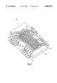
- an inventive die package 20includes a Leads-Over-Chip (LOC) lead frame 22 comprising an assembly of interdigitated leads 24 supported by a housing 26.
- LOCLeads-Over-Chip
- a portion of each of the leads 24extends across a front-side surface of an integrated circuit (IC) die 28 from one edge substantially to another, opposing edge in close proximity to adjacent leads 24 and is adhesively attached to the front-side surface using double-sided adhesive tape 30 so the leads 24 together support the IC die 28 within the die package 20.
- ICintegrated circuit
- the leads 24extend substantially from edge to edge across the front-side surface of the IC die 28 in close proximity to one another, a substantial area of the front-side surface (e.g., 30% to 80% or more) is adhesively attached to the leads 24, so the IC die 28 is supported in an improved manner, and heat is conducted away from the IC die 28 through the lead frame 22 in an improved manner.
- the die package 20is shown in FIG. 2 in the form of a Thin Small Outline Package (TSOP), the present invention is equally applicable to any die package including, for example, a Thin Quad Flat Pack (TQFP), a Small Outline J-lead (SOJ) package, a Plastic Leaded Chip Carrier (PLCC), and a Dual In-line Package (DIP).
- TQFPThin Quad Flat Pack
- SOJSmall Outline J-lead
- PLCCPlastic Leaded Chip Carrier
- DIPDual In-line Package
- leads 24 of the LOC lead frame 22are shown in FIG.
- lead frame leads and other support membershaving any shape and any arrangement that extend substantially from edge to opposing edge across the front-side surface of an IC die in adhesive attachment therewith.
- the present inventionincludes within its scope any support members extending across an IC die as described, not just support members, such as the leads 24, that serve as conductors for an IC die.
- the IC die 28may comprise any IC die, and that the double-sided adhesive tape 30 may comprise any adhesive tape for attaching the leads 24 to the frontside surface of the IC die 28.
- the leads 24are shown in FIG. 2 extending substantially from edge to edge across the IC die 28, the present invention includes within its scope lead frames in which only some of the leads extend substantially from edge to edge across an IC die.
- Each of the leads 24is wire-bonded to one of a multitude of bond pads on the front-side surface of the IC die 28, and each of the leads 24 extends from the die package 20 to terminate in a pin that may be connected to external circuitry (not shown) so circuitry within the IC die 28 may communicate with the external circuitry through the bond pads and the leads 24.
- one of the leads 24is wire-bonded at one end to an AO address bit bond pad on the front-side surface of the IC die 28 and extends from the die package 20 to terminate in an AO address bit pin.
- the leads 24are shown in FIG.
- a die package 40is identical to the die package 20 of FIG. 2, except that the pin-out arrangement of the die package 40 mirrors the pin-out arrangement of the die package 20 as a result of each of a plurality of interdigitated leads 44 being wire-bonded near its mid-point to an alternative bond pad on the front-side surface of an IC die 48.
- identical dice and LOC lead framescan be used to produce mirror image die packages.
- die packagesare advantageous because they can be placed on opposing sides of a base, such as a printed circuit Single In-line Memory Module (SIMM) board, with their common pins in alignment, thereby simplifying the routing of signals to the packages.
- SIMM boardis described below with respect to FIG. 5.
- the mirror image die packages 20 and 40 of FIGS. 2 and 3are shown in top plan views in FIGS. 4A and 4B, respectively, for clarity.
- an electronic device 50includes a portion of a base, such as a SIMM board 52, which includes the mirror image die packages 20 and 40 of FIGS. 2 and 3 attached to opposite sides of the board 52 with leads 24 and 44 associated with identical functions (e.g., DQ1, DQ2, and A4) opposing one another.
- a basesuch as a SIMM board 52
- leads 24 and 44associated with identical functions (e.g., DQ1, DQ2, and A4) opposing one another.
- DQ1, DQ2, and A4identical functions
- each of the leads 24 and 44typically has a function associated with it (or is a no-connection lead), as described above with respect to FIGS. 2, 3, 4A, and 4B.
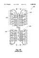
- an inventive die quad-package 60includes an LOC lead frame 62 comprising an assembly of interdigitated leads 64 supported by a housing 66.
- a portion of each of the leads 64extends across a front-side surface of an IC die 68 from one edge substantially to another, adjacent edge in close proximity to adjacent leads 64 and is adhesively attached to the front-side surface using double-sided adhesive tape 70 so the leads 64 together support the IC die 68 within the die quad-package 60.
- the leads 64extend substantially from edge to edge across the front-side surface of the IC die 68 in close proximity to one another, a substantial area of the front-side surface (e.g., 30% to 80% or more) is adhesively attached to the leads 64, so the IC die 68 is supported in an improved manner, and heat is conducted away from the IC die 68 through the lead frame 62 in an improved manner.
- a substantial area of the front-side surfacee.g., 30% to 80% or more
- the die quad-package 60is shown in FIG. 6 in the form of a Thin Quad Flat Pack (TQFP), the present invention is equally applicable to any die quad-package.
- the leads 64 of the LOC lead frame 62are shown in FIG. 6 having a particular shape and a particular arrangement with respect to one another, it will be understood that the present invention includes within its scope lead frame leads and other support members having any shape and any arrangement that extend substantially from edge to adjacent edge across the front-side surface of an IC die in adhesive attachment therewith.
- the present inventionincludes within its scope any support members extending across an IC die as described, not just support members, such as the leads 64, that serve as conductors for an IC die.
- the IC die 68may comprise any IC die
- the double-sided adhesive tape 70may comprise any adhesive tape for attaching the leads 64 to the front-side surface of the IC die 68.
- the present inventionincludes within its scope lead frames in which only some of the leads extend substantially from edge to edge across an IC die.
- Each of the leads 64is wire-bonded to one of a multitude of bond pads on the front-side surface of the IC die 68, and each of the leads 64 extends from the die quad-package 60 to terminate in a pin that may be connected to external circuitry (not shown) so circuitry within the IC die 68 may communicate with the external circuitry through the bond pads and the leads 64.
- one of the leads 64is wire-bonded at one end to an A0 address bit bond pad on the front-side surface of the IC die 68 and extends from the die quad-package 60 to terminate in an A0 address bit pin.
- the leads 64are shown in FIG.
- a die quad-package 80is identical to the die quad-package 60 of FIG. 6, except that the pin-out arrangement of the die quad-package 80 mirrors the pin-out arrangement of the die quad-package 60 as a result of each of a plurality of interdigitated leads 84 being wire-bonded near its mid-point to an alternative bond pad on the front-side surface of an IC die 88.
- identical dice and LOC lead framescan be used to produce mirror image die quad-packages.
- such die quad-packagesare advantageous because they can be placed on opposing sides of a base, such as a printed circuit Single In-line Memory Module (SIMM) board, with their common pins in alignment, thereby simplifying the routing of signals to the quad-packages.
- SIMMSingle In-line Memory Module
- the mirror image die quad-packages 60 and 80 of FIGS. 6 and 7are shown in top plan views in FIGS. 8A and 8B, respectively, for clarity.
- the die quad-package 80 of FIG. 7is also shown turned clockwise by 90° in a top plan view in FIG. 8C in order to illustrate more clearly the mirror image relationship between the die quad-package 60 of FIG. 6 and the die quad-package 80 of FIG. 7.
- various operative configurations of an IC die and lead frame, other than mirror imagesmay be obtained using the same IC die and lead frame design.
- an electronic device 90includes a portion of a base, such as a SIMM board 92, which includes the mirror image die quad-packages 60 and 80 of FIGS. 6 and 7 attached to opposite sides of the board 92 with leads 64 and 84 associated with identical functions (e.g., V cc , A2, and A5) opposing one another.
- a basesuch as a SIMM board 92
- leads 64 and 84associated with identical functions (e.g., V cc , A2, and A5) opposing one another.
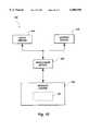
- the die quad-package 60 of FIG. 6is incorporated into a memory device 100 in an electronic system 102, such as a computer system, that also includes an input device 104, an output device 106, and a processor device 108.
- an electronic system 102such as a computer system
- the die quad-package 60is shown in FIG. 10 incorporated into the memory device 100, it may also be incorporated into any one of the input, output, and processor devices 104, 106, and 108.
- the electronic system 102may include any one of the packages 20, 40, and 80 of FIGS. 2, 3, 4A, 4B, 5, 7, 8A, 8B, 8C, and 9 instead of, or in addition to, the package 60 of FIG. 6.
- the present inventionprovides an LOC lead frame and other devices and methods for supporting IC dice in an improved manner.
- the inventive LOC lead frameis capable of producing mirror image die packages, if desired, using identical dice having a wide variety of different bond pad arrangements.
- the inventive lead frameis also capable of conducting heat away from a die in an improved manner.
Landscapes
- Physics & Mathematics (AREA)
- Condensed Matter Physics & Semiconductors (AREA)
- General Physics & Mathematics (AREA)
- Engineering & Computer Science (AREA)
- Computer Hardware Design (AREA)
- Microelectronics & Electronic Packaging (AREA)
- Power Engineering (AREA)
- Lead Frames For Integrated Circuits (AREA)
Abstract
Description
Claims (3)
Priority Applications (2)
| Application Number | Priority Date | Filing Date | Title |
|---|---|---|---|
| US09/271,752US6008996A (en) | 1997-04-07 | 1999-03-18 | Interdigitated leads-over-chip lead frame, device, and method for supporting an integrated circuit die |
| US09/450,069US6344976B1 (en) | 1997-04-07 | 1999-11-29 | Interdigitated leads-over-chip lead frame device and method for supporting an integrated circuit die |
Applications Claiming Priority (3)
| Application Number | Priority Date | Filing Date | Title |
|---|---|---|---|
| US08/827,886US6271582B1 (en) | 1997-04-07 | 1997-04-07 | Interdigitated leads-over-chip lead frame, device, and method for supporting an integrated circuit die |
| US09/141,001US5903443A (en) | 1997-04-07 | 1998-08-26 | Interdigitated leads-over-chip lead frame, device, and method for supporting an integrated circuit die |
| US09/271,752US6008996A (en) | 1997-04-07 | 1999-03-18 | Interdigitated leads-over-chip lead frame, device, and method for supporting an integrated circuit die |
Related Parent Applications (1)
| Application Number | Title | Priority Date | Filing Date |
|---|---|---|---|
| US09/141,001ContinuationUS5903443A (en) | 1997-04-07 | 1998-08-26 | Interdigitated leads-over-chip lead frame, device, and method for supporting an integrated circuit die |
Related Child Applications (1)
| Application Number | Title | Priority Date | Filing Date |
|---|---|---|---|
| US09/450,069ContinuationUS6344976B1 (en) | 1997-04-07 | 1999-11-29 | Interdigitated leads-over-chip lead frame device and method for supporting an integrated circuit die |
Publications (1)
| Publication Number | Publication Date |
|---|---|
| US6008996Atrue US6008996A (en) | 1999-12-28 |
Family
ID=26838695
Family Applications (2)
| Application Number | Title | Priority Date | Filing Date |
|---|---|---|---|
| US09/271,752Expired - LifetimeUS6008996A (en) | 1997-04-07 | 1999-03-18 | Interdigitated leads-over-chip lead frame, device, and method for supporting an integrated circuit die |
| US09/450,069Expired - Fee RelatedUS6344976B1 (en) | 1997-04-07 | 1999-11-29 | Interdigitated leads-over-chip lead frame device and method for supporting an integrated circuit die |
Family Applications After (1)
| Application Number | Title | Priority Date | Filing Date |
|---|---|---|---|
| US09/450,069Expired - Fee RelatedUS6344976B1 (en) | 1997-04-07 | 1999-11-29 | Interdigitated leads-over-chip lead frame device and method for supporting an integrated circuit die |
Country Status (1)
| Country | Link |
|---|---|
| US (2) | US6008996A (en) |
Cited By (4)
| Publication number | Priority date | Publication date | Assignee | Title |
|---|---|---|---|---|
| US6541846B2 (en) | 2000-09-01 | 2003-04-01 | Micron Technology, Inc. | Dual LOC semiconductor assembly employing floating lead finger structure |
| US20030193081A1 (en)* | 1997-04-07 | 2003-10-16 | Aaron Schoenfeld | Interdigitated leads-over-chip lead frame and device for supporting an integrated circuit die |
| US20170245361A1 (en)* | 2016-01-06 | 2017-08-24 | Nokomis, Inc. | Electronic device and methods to customize electronic device electromagnetic emissions |
| US20190103313A1 (en)* | 2017-10-03 | 2019-04-04 | Ubotic Company Limited | Carrier substrate, package, and method of manufacture |
Families Citing this family (61)
| Publication number | Priority date | Publication date | Assignee | Title |
|---|---|---|---|---|
| US6429528B1 (en)* | 1998-02-27 | 2002-08-06 | Micron Technology, Inc. | Multichip semiconductor package |
| US6114756A (en)* | 1998-04-01 | 2000-09-05 | Micron Technology, Inc. | Interdigitated capacitor design for integrated circuit leadframes |
| US6670719B2 (en) | 1999-08-25 | 2003-12-30 | Micron Technology, Inc. | Microelectronic device package filled with liquid or pressurized gas and associated method of manufacture |
| US6709968B1 (en) | 2000-08-16 | 2004-03-23 | Micron Technology, Inc. | Microelectronic device with package with conductive elements and associated method of manufacture |
| US6576494B1 (en)* | 2000-06-28 | 2003-06-10 | Micron Technology, Inc. | Recessed encapsulated microelectronic devices and methods for formation |
| US7273769B1 (en)* | 2000-08-16 | 2007-09-25 | Micron Technology, Inc. | Method and apparatus for removing encapsulating material from a packaged microelectronic device |
| US7183138B2 (en)* | 2000-08-23 | 2007-02-27 | Micron Technology, Inc. | Method and apparatus for decoupling conductive portions of a microelectronic device package |
| US6564979B2 (en) | 2001-07-18 | 2003-05-20 | Micron Technology, Inc. | Method and apparatus for dispensing adhesive on microelectronic substrate supports |
| US6437431B1 (en)* | 2001-08-07 | 2002-08-20 | Lsi Logic Corporation | Die power distribution system |
| SG111919A1 (en)* | 2001-08-29 | 2005-06-29 | Micron Technology Inc | Packaged microelectronic devices and methods of forming same |
| US20030042615A1 (en) | 2001-08-30 | 2003-03-06 | Tongbi Jiang | Stacked microelectronic devices and methods of fabricating same |
| US6870276B1 (en)* | 2001-12-26 | 2005-03-22 | Micron Technology, Inc. | Apparatus for supporting microelectronic substrates |
| US6896760B1 (en)* | 2002-01-16 | 2005-05-24 | Micron Technology, Inc. | Fabrication of stacked microelectronic devices |
| US6673649B1 (en)* | 2002-07-05 | 2004-01-06 | Micron Technology, Inc. | Microelectronic device packages and methods for controlling the disposition of non-conductive materials in such packages |
| US7067905B2 (en)* | 2002-08-08 | 2006-06-27 | Micron Technology, Inc. | Packaged microelectronic devices including first and second casings |
| SG120879A1 (en)* | 2002-08-08 | 2006-04-26 | Micron Technology Inc | Packaged microelectronic components |
| SG114585A1 (en)* | 2002-11-22 | 2005-09-28 | Micron Technology Inc | Packaged microelectronic component assemblies |
| JP3793143B2 (en)* | 2002-11-28 | 2006-07-05 | 株式会社シマノ | Bicycle electronic control device |
| US7132734B2 (en)* | 2003-01-06 | 2006-11-07 | Micron Technology, Inc. | Microelectronic component assemblies and microelectronic component lead frame structures |
| US6879050B2 (en)* | 2003-02-11 | 2005-04-12 | Micron Technology, Inc. | Packaged microelectronic devices and methods for packaging microelectronic devices |
| US6967390B2 (en)* | 2003-02-13 | 2005-11-22 | Freescale Semiconductor, Inc. | Electronic component and method of manufacturing same |
| SG143931A1 (en) | 2003-03-04 | 2008-07-29 | Micron Technology Inc | Microelectronic component assemblies employing lead frames having reduced-thickness inner lengths |
| US7183485B2 (en)* | 2003-03-11 | 2007-02-27 | Micron Technology, Inc. | Microelectronic component assemblies having lead frames adapted to reduce package bow |
| US7102217B2 (en) | 2003-04-09 | 2006-09-05 | Micron Technology, Inc. | Interposer substrates with reinforced interconnect slots, and semiconductor die packages including same |
| SG143932A1 (en)* | 2003-05-30 | 2008-07-29 | Micron Technology Inc | Packaged microelectronic devices and methods of packaging microelectronic devices |
| US7368810B2 (en)* | 2003-08-29 | 2008-05-06 | Micron Technology, Inc. | Invertible microfeature device packages |
| US7071421B2 (en) | 2003-08-29 | 2006-07-04 | Micron Technology, Inc. | Stacked microfeature devices and associated methods |
| US7565141B2 (en)* | 2003-10-08 | 2009-07-21 | Macaluso Anthony G | Over the air provisioning of mobile device settings |
| US6888719B1 (en)* | 2003-10-16 | 2005-05-03 | Micron Technology, Inc. | Methods and apparatuses for transferring heat from microelectronic device modules |
| US8084866B2 (en) | 2003-12-10 | 2011-12-27 | Micron Technology, Inc. | Microelectronic devices and methods for filling vias in microelectronic devices |
| US7091124B2 (en)* | 2003-11-13 | 2006-08-15 | Micron Technology, Inc. | Methods for forming vias in microelectronic devices, and methods for packaging microelectronic devices |
| US20050247894A1 (en) | 2004-05-05 | 2005-11-10 | Watkins Charles M | Systems and methods for forming apertures in microfeature workpieces |
| US7289332B2 (en)* | 2004-06-16 | 2007-10-30 | Liberty University | Mirror image electrical packages and system for using same |
| US7232754B2 (en) | 2004-06-29 | 2007-06-19 | Micron Technology, Inc. | Microelectronic devices and methods for forming interconnects in microelectronic devices |
| SG145547A1 (en) | 2004-07-23 | 2008-09-29 | Micron Technology Inc | Microelectronic component assemblies with recessed wire bonds and methods of making same |
| US7632747B2 (en)* | 2004-08-19 | 2009-12-15 | Micron Technology, Inc. | Conductive structures for microfeature devices and methods for fabricating microfeature devices |
| US7425499B2 (en)* | 2004-08-24 | 2008-09-16 | Micron Technology, Inc. | Methods for forming interconnects in vias and microelectronic workpieces including such interconnects |
| US7602618B2 (en)* | 2004-08-25 | 2009-10-13 | Micron Technology, Inc. | Methods and apparatuses for transferring heat from stacked microfeature devices |
| SG120200A1 (en) | 2004-08-27 | 2006-03-28 | Micron Technology Inc | Slanted vias for electrical circuits on circuit boards and other substrates |
| US7095122B2 (en)* | 2004-09-01 | 2006-08-22 | Micron Technology, Inc. | Reduced-dimension microelectronic component assemblies with wire bonds and methods of making same |
| US7300857B2 (en) | 2004-09-02 | 2007-11-27 | Micron Technology, Inc. | Through-wafer interconnects for photoimager and memory wafers |
| US7271482B2 (en) | 2004-12-30 | 2007-09-18 | Micron Technology, Inc. | Methods for forming interconnects in microelectronic workpieces and microelectronic workpieces formed using such methods |
| US7795134B2 (en) | 2005-06-28 | 2010-09-14 | Micron Technology, Inc. | Conductive interconnect structures and formation methods using supercritical fluids |
| US7262134B2 (en) | 2005-09-01 | 2007-08-28 | Micron Technology, Inc. | Microfeature workpieces and methods for forming interconnects in microfeature workpieces |
| US7622377B2 (en) | 2005-09-01 | 2009-11-24 | Micron Technology, Inc. | Microfeature workpiece substrates having through-substrate vias, and associated methods of formation |
| US7863187B2 (en) | 2005-09-01 | 2011-01-04 | Micron Technology, Inc. | Microfeature workpieces and methods for forming interconnects in microfeature workpieces |
| US20070148820A1 (en)* | 2005-12-22 | 2007-06-28 | Micron Technology, Inc. | Microelectronic devices and methods for manufacturing microelectronic devices |
| SG135074A1 (en) | 2006-02-28 | 2007-09-28 | Micron Technology Inc | Microelectronic devices, stacked microelectronic devices, and methods for manufacturing such devices |
| SG135979A1 (en)* | 2006-03-08 | 2007-10-29 | Micron Technology Inc | Microelectronic device assemblies including assemblies with recurved leadframes, and associated methods |
| US7749899B2 (en) | 2006-06-01 | 2010-07-06 | Micron Technology, Inc. | Microelectronic workpieces and methods and systems for forming interconnects in microelectronic workpieces |
| SG138501A1 (en)* | 2006-07-05 | 2008-01-28 | Micron Technology Inc | Lead frames, microelectronic devices with lead frames, and methods for manufacturing lead frames and microelectronic devices with lead frames |
| SG139573A1 (en)* | 2006-07-17 | 2008-02-29 | Micron Technology Inc | Microelectronic packages with leadframes, including leadframes configured for stacked die packages, and associated systems and methods |
| US7629249B2 (en)* | 2006-08-28 | 2009-12-08 | Micron Technology, Inc. | Microfeature workpieces having conductive interconnect structures formed by chemically reactive processes, and associated systems and methods |
| US7902643B2 (en) | 2006-08-31 | 2011-03-08 | Micron Technology, Inc. | Microfeature workpieces having interconnects and conductive backplanes, and associated systems and methods |
| US7750449B2 (en)* | 2007-03-13 | 2010-07-06 | Micron Technology, Inc. | Packaged semiconductor components having substantially rigid support members and methods of packaging semiconductor components |
| SG149724A1 (en)* | 2007-07-24 | 2009-02-27 | Micron Technology Inc | Semicoductor dies with recesses, associated leadframes, and associated systems and methods |
| SG149725A1 (en)* | 2007-07-24 | 2009-02-27 | Micron Technology Inc | Thin semiconductor die packages and associated systems and methods |
| SG149726A1 (en) | 2007-07-24 | 2009-02-27 | Micron Technology Inc | Microelectronic die packages with metal leads, including metal leads for stacked die packages, and associated systems and methods |
| SG150396A1 (en) | 2007-08-16 | 2009-03-30 | Micron Technology Inc | Microelectronic die packages with leadframes, including leadframe-based interposer for stacked die packages, and associated systems and methods |
| SG150410A1 (en) | 2007-08-31 | 2009-03-30 | Micron Technology Inc | Partitioned through-layer via and associated systems and methods |
| US7884015B2 (en) | 2007-12-06 | 2011-02-08 | Micron Technology, Inc. | Methods for forming interconnects in microelectronic workpieces and microelectronic workpieces formed using such methods |
Citations (29)
| Publication number | Priority date | Publication date | Assignee | Title |
|---|---|---|---|---|
| US4862245A (en)* | 1985-04-18 | 1989-08-29 | International Business Machines Corporation | Package semiconductor chip |
| US4937656A (en)* | 1988-04-22 | 1990-06-26 | Mitsubishi Denki Kabushiki Kaisha | Semiconductor device |
| US4949161A (en)* | 1988-12-23 | 1990-08-14 | Micron Technology, Inc. | Interdigitized leadframe strip |
| US5086018A (en)* | 1991-05-02 | 1992-02-04 | International Business Machines Corporation | Method of making a planarized thin film covered wire bonded semiconductor package |
| US5147815A (en)* | 1990-05-14 | 1992-09-15 | Motorola, Inc. | Method for fabricating a multichip semiconductor device having two interdigitated leadframes |
| JPH05109979A (en)* | 1991-10-15 | 1993-04-30 | Mitsubishi Electric Corp | INVERTING IC MANUFACTURING METHOD AND IC MODULE USING THE SAME |
| US5218168A (en)* | 1991-09-26 | 1993-06-08 | Micron Technology, Inc. | Leads over tab |
| US5250840A (en)* | 1992-02-24 | 1993-10-05 | Samsung Electronics Co., Ltd. | Semiconductor lead frame with a chip having bonding pads in a cross arrangement |
| US5256598A (en)* | 1992-04-15 | 1993-10-26 | Micron Technology, Inc. | Shrink accommodating lead frame |
| US5327009A (en)* | 1992-05-22 | 1994-07-05 | Nec Corporation | Miniaturized integrated circuit package |
| US5331200A (en)* | 1992-09-30 | 1994-07-19 | Texas Instruments Incorporated | Lead-on-chip inner lead bonding lead frame method and apparatus |
| US5360992A (en)* | 1991-12-20 | 1994-11-01 | Micron Technology, Inc. | Two piece assembly for the selection of pinouts and bond options on a semiconductor device |
| US5381036A (en)* | 1992-02-03 | 1995-01-10 | Motorola, Inc. | Lead-on chip semiconductor device having peripheral bond pads |
| US5384488A (en)* | 1992-06-15 | 1995-01-24 | Texas Instruments Incorporated | Configuration and method for positioning semiconductor device bond pads using additional process layers |
| US5434106A (en)* | 1989-12-22 | 1995-07-18 | Texas Instruments Incorporated | Integrated circuit device and method to prevent cracking during surface mount |
| US5438478A (en)* | 1992-10-20 | 1995-08-01 | Ibiden Co., Ltd. | Electronic component carriers and method of producing the same as well as electronic devices |
| US5508565A (en)* | 1992-12-18 | 1996-04-16 | Fujitsu Limited | Semiconductor device having a plurality of chips having identical circuit arrangement sealed in package |
| US5521426A (en)* | 1992-09-09 | 1996-05-28 | Texas Instruments Incorporated | Reduced capacitance lead frame for lead on chip package |
| US5523617A (en)* | 1994-12-27 | 1996-06-04 | National Semiconductor Corporation | Fuse frames, programmable fuse frames, and methods for programming by fusing |
| US5528075A (en)* | 1991-08-15 | 1996-06-18 | Staktek Corporation | Lead-on-chip integrated circuit apparatus |
| US5530292A (en)* | 1990-03-15 | 1996-06-25 | Fujitsu Limited | Semiconductor device having a plurality of chips |
| US5563443A (en)* | 1993-03-13 | 1996-10-08 | Texas Instruments Incorporated | Packaged semiconductor device utilizing leadframe attached on a semiconductor chip |
| US5585667A (en)* | 1994-12-23 | 1996-12-17 | National Semiconductor Corporation | Lead frame for handling crossing bonding wires |
| US5585668A (en)* | 1995-01-30 | 1996-12-17 | Staktek Corporation | Integrated circuit package with overlapped die on a common lead frame |
| US5612259A (en)* | 1993-07-29 | 1997-03-18 | Kabushiki Kaisha Toshiba | Method for manufacturing a semiconductor device wherein a semiconductor chip is mounted on a lead frame |
| US5637915A (en)* | 1991-12-27 | 1997-06-10 | Fujitsu Ltd. | Semiconductor device affixed to an upper and a lower leadframe |
| US5696665A (en)* | 1994-07-01 | 1997-12-09 | Saint-Gobain/Norton Industrial Ceramics Corporation | Integrated circuit package with diamond heat sink |
| US5780925A (en)* | 1992-10-28 | 1998-07-14 | International Business Machines Corporation | Lead frame package for electronic devices |
| US5804870A (en)* | 1992-06-26 | 1998-09-08 | Staktek Corporation | Hermetically sealed integrated circuit lead-on package configuration |
Family Cites Families (7)
| Publication number | Priority date | Publication date | Assignee | Title |
|---|---|---|---|---|
| US5234866A (en) | 1985-03-25 | 1993-08-10 | Hitachi, Ltd. | Semiconductor device and process for producing the same, and lead frame used in said process |
| US5365113A (en)* | 1987-06-30 | 1994-11-15 | Hitachi, Ltd. | Semiconductor device |
| JP2528991B2 (en)* | 1990-02-28 | 1996-08-28 | 株式会社日立製作所 | Resin-sealed semiconductor device and lead frame |
| KR940006164B1 (en)* | 1991-05-11 | 1994-07-08 | 금성일렉트론 주식회사 | Semiconductor package and manufacturing method |
| US5811875A (en)* | 1995-06-29 | 1998-09-22 | Samsung Electronics Co., Ltd. | Lead frames including extended tie-bars, and semiconductor chip packages using same |
| JPH09102575A (en)* | 1995-09-11 | 1997-04-15 | Internatl Business Mach Corp <Ibm> | Lead frame structure of lead-on chip without jump on wiring |
| US6462404B1 (en)* | 1997-02-28 | 2002-10-08 | Micron Technology, Inc. | Multilevel leadframe for a packaged integrated circuit |
- 1999
- 1999-03-18USUS09/271,752patent/US6008996A/ennot_activeExpired - Lifetime
- 1999-11-29USUS09/450,069patent/US6344976B1/ennot_activeExpired - Fee Related
Patent Citations (30)
| Publication number | Priority date | Publication date | Assignee | Title |
|---|---|---|---|---|
| US4862245A (en)* | 1985-04-18 | 1989-08-29 | International Business Machines Corporation | Package semiconductor chip |
| US4937656A (en)* | 1988-04-22 | 1990-06-26 | Mitsubishi Denki Kabushiki Kaisha | Semiconductor device |
| US4949161A (en)* | 1988-12-23 | 1990-08-14 | Micron Technology, Inc. | Interdigitized leadframe strip |
| US5434106A (en)* | 1989-12-22 | 1995-07-18 | Texas Instruments Incorporated | Integrated circuit device and method to prevent cracking during surface mount |
| US5530292A (en)* | 1990-03-15 | 1996-06-25 | Fujitsu Limited | Semiconductor device having a plurality of chips |
| US5147815A (en)* | 1990-05-14 | 1992-09-15 | Motorola, Inc. | Method for fabricating a multichip semiconductor device having two interdigitated leadframes |
| US5086018A (en)* | 1991-05-02 | 1992-02-04 | International Business Machines Corporation | Method of making a planarized thin film covered wire bonded semiconductor package |
| US5528075A (en)* | 1991-08-15 | 1996-06-18 | Staktek Corporation | Lead-on-chip integrated circuit apparatus |
| US5218168A (en)* | 1991-09-26 | 1993-06-08 | Micron Technology, Inc. | Leads over tab |
| US5303120A (en)* | 1991-10-15 | 1994-04-12 | Mitsubishi Denki Kabushiki Kaisha | Method of manufacturing inversion type IC's and IC module using same |
| JPH05109979A (en)* | 1991-10-15 | 1993-04-30 | Mitsubishi Electric Corp | INVERTING IC MANUFACTURING METHOD AND IC MODULE USING THE SAME |
| US5360992A (en)* | 1991-12-20 | 1994-11-01 | Micron Technology, Inc. | Two piece assembly for the selection of pinouts and bond options on a semiconductor device |
| US5637915A (en)* | 1991-12-27 | 1997-06-10 | Fujitsu Ltd. | Semiconductor device affixed to an upper and a lower leadframe |
| US5381036A (en)* | 1992-02-03 | 1995-01-10 | Motorola, Inc. | Lead-on chip semiconductor device having peripheral bond pads |
| US5250840A (en)* | 1992-02-24 | 1993-10-05 | Samsung Electronics Co., Ltd. | Semiconductor lead frame with a chip having bonding pads in a cross arrangement |
| US5256598A (en)* | 1992-04-15 | 1993-10-26 | Micron Technology, Inc. | Shrink accommodating lead frame |
| US5327009A (en)* | 1992-05-22 | 1994-07-05 | Nec Corporation | Miniaturized integrated circuit package |
| US5384488A (en)* | 1992-06-15 | 1995-01-24 | Texas Instruments Incorporated | Configuration and method for positioning semiconductor device bond pads using additional process layers |
| US5804870A (en)* | 1992-06-26 | 1998-09-08 | Staktek Corporation | Hermetically sealed integrated circuit lead-on package configuration |
| US5521426A (en)* | 1992-09-09 | 1996-05-28 | Texas Instruments Incorporated | Reduced capacitance lead frame for lead on chip package |
| US5331200A (en)* | 1992-09-30 | 1994-07-19 | Texas Instruments Incorporated | Lead-on-chip inner lead bonding lead frame method and apparatus |
| US5438478A (en)* | 1992-10-20 | 1995-08-01 | Ibiden Co., Ltd. | Electronic component carriers and method of producing the same as well as electronic devices |
| US5780925A (en)* | 1992-10-28 | 1998-07-14 | International Business Machines Corporation | Lead frame package for electronic devices |
| US5508565A (en)* | 1992-12-18 | 1996-04-16 | Fujitsu Limited | Semiconductor device having a plurality of chips having identical circuit arrangement sealed in package |
| US5563443A (en)* | 1993-03-13 | 1996-10-08 | Texas Instruments Incorporated | Packaged semiconductor device utilizing leadframe attached on a semiconductor chip |
| US5612259A (en)* | 1993-07-29 | 1997-03-18 | Kabushiki Kaisha Toshiba | Method for manufacturing a semiconductor device wherein a semiconductor chip is mounted on a lead frame |
| US5696665A (en)* | 1994-07-01 | 1997-12-09 | Saint-Gobain/Norton Industrial Ceramics Corporation | Integrated circuit package with diamond heat sink |
| US5585667A (en)* | 1994-12-23 | 1996-12-17 | National Semiconductor Corporation | Lead frame for handling crossing bonding wires |
| US5523617A (en)* | 1994-12-27 | 1996-06-04 | National Semiconductor Corporation | Fuse frames, programmable fuse frames, and methods for programming by fusing |
| US5585668A (en)* | 1995-01-30 | 1996-12-17 | Staktek Corporation | Integrated circuit package with overlapped die on a common lead frame |
Cited By (7)
| Publication number | Priority date | Publication date | Assignee | Title |
|---|---|---|---|---|
| US20030193081A1 (en)* | 1997-04-07 | 2003-10-16 | Aaron Schoenfeld | Interdigitated leads-over-chip lead frame and device for supporting an integrated circuit die |
| US6831353B2 (en) | 1997-04-07 | 2004-12-14 | Micron Technology, Inc. | Interdigitated leads-over-chip lead frame and device for supporting an integrated circuit die |
| US6541846B2 (en) | 2000-09-01 | 2003-04-01 | Micron Technology, Inc. | Dual LOC semiconductor assembly employing floating lead finger structure |
| US6762079B2 (en) | 2000-09-01 | 2004-07-13 | Micron Technology, Inc. | Methods for fabricating dual loc semiconductor die assembly employing floating lead finger structure |
| US20170245361A1 (en)* | 2016-01-06 | 2017-08-24 | Nokomis, Inc. | Electronic device and methods to customize electronic device electromagnetic emissions |
| US20190103313A1 (en)* | 2017-10-03 | 2019-04-04 | Ubotic Company Limited | Carrier substrate, package, and method of manufacture |
| US10777457B2 (en)* | 2017-10-03 | 2020-09-15 | Ubotic Company Limited | Carrier substrate, package, and method of manufacture |
Also Published As
| Publication number | Publication date |
|---|---|
| US6344976B1 (en) | 2002-02-05 |
Similar Documents
| Publication | Publication Date | Title |
|---|---|---|
| US6008996A (en) | Interdigitated leads-over-chip lead frame, device, and method for supporting an integrated circuit die | |
| US5903443A (en) | Interdigitated leads-over-chip lead frame, device, and method for supporting an integrated circuit die | |
| JP2537014B2 (en) | Lead frame package for electronic devices | |
| US6858472B2 (en) | Method for implementing selected functionality on an integrated circuit device | |
| US6847100B2 (en) | High speed IC package configuration | |
| US5637828A (en) | High density semiconductor package | |
| KR970006529B1 (en) | Semiconductor device | |
| US6724074B2 (en) | Stack semiconductor chip package and lead frame | |
| KR100328906B1 (en) | Method and device for joining leads inside lead-on chip of leadframe | |
| US6442040B2 (en) | Embedded memory assembly | |
| US6052289A (en) | Interdigitated leads-over-chip lead frame for supporting an integrated circuit die | |
| JP2896223B2 (en) | Resin-sealed semiconductor device | |
| JP2871984B2 (en) | Semiconductor device | |
| JP2796119B2 (en) | Semiconductor devices and memory module devices | |
| JP2004228259A (en) | Semiconductor device and electronic device using the same | |
| KR970003906A (en) | Thin film tape with tape pad and semiconductor device using same | |
| KR20030046933A (en) | Stack package | |
| JPH03200360A (en) | Integrated circuit module | |
| JPH0697360A (en) | Semiconductor integrated circuit device | |
| JPH10270495A (en) | Semiconductor device |
Legal Events
| Date | Code | Title | Description |
|---|---|---|---|
| STCF | Information on status: patent grant | Free format text:PATENTED CASE | |
| CC | Certificate of correction | ||
| FPAY | Fee payment | Year of fee payment:4 | |
| FEPP | Fee payment procedure | Free format text:PAYOR NUMBER ASSIGNED (ORIGINAL EVENT CODE: ASPN); ENTITY STATUS OF PATENT OWNER: LARGE ENTITY | |
| FPAY | Fee payment | Year of fee payment:8 | |
| FPAY | Fee payment | Year of fee payment:12 | |
| AS | Assignment | Owner name:U.S. BANK NATIONAL ASSOCIATION, AS COLLATERAL AGENT, CALIFORNIA Free format text:SECURITY INTEREST;ASSIGNOR:MICRON TECHNOLOGY, INC.;REEL/FRAME:038669/0001 Effective date:20160426 Owner name:U.S. BANK NATIONAL ASSOCIATION, AS COLLATERAL AGEN Free format text:SECURITY INTEREST;ASSIGNOR:MICRON TECHNOLOGY, INC.;REEL/FRAME:038669/0001 Effective date:20160426 | |
| AS | Assignment | Owner name:MORGAN STANLEY SENIOR FUNDING, INC., AS COLLATERAL AGENT, MARYLAND Free format text:PATENT SECURITY AGREEMENT;ASSIGNOR:MICRON TECHNOLOGY, INC.;REEL/FRAME:038954/0001 Effective date:20160426 Owner name:MORGAN STANLEY SENIOR FUNDING, INC., AS COLLATERAL Free format text:PATENT SECURITY AGREEMENT;ASSIGNOR:MICRON TECHNOLOGY, INC.;REEL/FRAME:038954/0001 Effective date:20160426 | |
| AS | Assignment | Owner name:U.S. BANK NATIONAL ASSOCIATION, AS COLLATERAL AGENT, CALIFORNIA Free format text:CORRECTIVE ASSIGNMENT TO CORRECT THE REPLACE ERRONEOUSLY FILED PATENT #7358718 WITH THE CORRECT PATENT #7358178 PREVIOUSLY RECORDED ON REEL 038669 FRAME 0001. ASSIGNOR(S) HEREBY CONFIRMS THE SECURITY INTEREST;ASSIGNOR:MICRON TECHNOLOGY, INC.;REEL/FRAME:043079/0001 Effective date:20160426 Owner name:U.S. BANK NATIONAL ASSOCIATION, AS COLLATERAL AGEN Free format text:CORRECTIVE ASSIGNMENT TO CORRECT THE REPLACE ERRONEOUSLY FILED PATENT #7358718 WITH THE CORRECT PATENT #7358178 PREVIOUSLY RECORDED ON REEL 038669 FRAME 0001. ASSIGNOR(S) HEREBY CONFIRMS THE SECURITY INTEREST;ASSIGNOR:MICRON TECHNOLOGY, INC.;REEL/FRAME:043079/0001 Effective date:20160426 | |
| AS | Assignment | Owner name:MICRON TECHNOLOGY, INC., IDAHO Free format text:RELEASE BY SECURED PARTY;ASSIGNOR:U.S. BANK NATIONAL ASSOCIATION, AS COLLATERAL AGENT;REEL/FRAME:047243/0001 Effective date:20180629 | |
| AS | Assignment | Owner name:MICRON TECHNOLOGY, INC., IDAHO Free format text:RELEASE BY SECURED PARTY;ASSIGNOR:MORGAN STANLEY SENIOR FUNDING, INC., AS COLLATERAL AGENT;REEL/FRAME:050937/0001 Effective date:20190731 |