US6008123A - Method for using a hardmask to form an opening in a semiconductor substrate - Google Patents
Method for using a hardmask to form an opening in a semiconductor substrateDownload PDFInfo
- Publication number
- US6008123A US6008123AUS08/963,687US96368797AUS6008123AUS 6008123 AUS6008123 AUS 6008123AUS 96368797 AUS96368797 AUS 96368797AUS 6008123 AUS6008123 AUS 6008123A
- Authority
- US
- United States
- Prior art keywords
- layer
- forming
- amorphous silicon
- opening
- recited
- Prior art date
- Legal status (The legal status is an assumption and is not a legal conclusion. Google has not performed a legal analysis and makes no representation as to the accuracy of the status listed.)
- Expired - Lifetime
Links
- 238000000034methodMethods0.000titleclaimsabstractdescription68
- 239000004065semiconductorSubstances0.000titleclaimsabstractdescription26
- 239000000758substrateSubstances0.000titledescription7
- 239000004020conductorSubstances0.000claimsabstractdescription25
- 238000000151depositionMethods0.000claimsabstractdescription24
- 125000006850spacer groupChemical group0.000claimsabstractdescription19
- 229910021417amorphous siliconInorganic materials0.000claimsdescription39
- 239000002002slurrySubstances0.000claimsdescription19
- 229910052710siliconInorganic materials0.000claimsdescription17
- 239000010703siliconSubstances0.000claimsdescription17
- 229910052751metalInorganic materials0.000claimsdescription16
- 239000002184metalSubstances0.000claimsdescription16
- KWYUFKZDYYNOTN-UHFFFAOYSA-MPotassium hydroxideChemical compound[OH-].[K+]KWYUFKZDYYNOTN-UHFFFAOYSA-M0.000claimsdescription12
- 239000010936titaniumSubstances0.000claimsdescription11
- MHAJPDPJQMAIIY-UHFFFAOYSA-NHydrogen peroxideChemical compoundOOMHAJPDPJQMAIIY-UHFFFAOYSA-N0.000claimsdescription10
- VYPSYNLAJGMNEJ-UHFFFAOYSA-NSilicium dioxideChemical compoundO=[Si]=OVYPSYNLAJGMNEJ-UHFFFAOYSA-N0.000claimsdescription10
- VCJMYUPGQJHHFU-UHFFFAOYSA-Niron(3+);trinitrateChemical compound[Fe+3].[O-][N+]([O-])=O.[O-][N+]([O-])=O.[O-][N+]([O-])=OVCJMYUPGQJHHFU-UHFFFAOYSA-N0.000claimsdescription10
- NRTOMJZYCJJWKI-UHFFFAOYSA-NTitanium nitrideChemical compound[Ti]#NNRTOMJZYCJJWKI-UHFFFAOYSA-N0.000claimsdescription9
- 239000007800oxidant agentSubstances0.000claimsdescription9
- QGZKDVFQNNGYKY-UHFFFAOYSA-NAmmoniaChemical compoundNQGZKDVFQNNGYKY-UHFFFAOYSA-N0.000claimsdescription8
- RTAQQCXQSZGOHL-UHFFFAOYSA-NTitaniumChemical compound[Ti]RTAQQCXQSZGOHL-UHFFFAOYSA-N0.000claimsdescription7
- 238000005530etchingMethods0.000claimsdescription7
- 229910052719titaniumInorganic materials0.000claimsdescription7
- 239000000377silicon dioxideSubstances0.000claimsdescription5
- WFKWXMTUELFFGS-UHFFFAOYSA-NtungstenChemical compound[W]WFKWXMTUELFFGS-UHFFFAOYSA-N0.000claimsdescription5
- 229910052721tungstenInorganic materials0.000claimsdescription5
- 239000010937tungstenSubstances0.000claimsdescription5
- 229910021529ammoniaInorganic materials0.000claimsdescription4
- TWNQGVIAIRXVLR-UHFFFAOYSA-Noxo(oxoalumanyloxy)alumaneChemical compoundO=[Al]O[Al]=OTWNQGVIAIRXVLR-UHFFFAOYSA-N0.000claimsdescription4
- 229910018404Al2 O3Inorganic materials0.000claimsdescription3
- 235000012239silicon dioxideNutrition0.000claims1
- 229920002120photoresistant polymerPolymers0.000description24
- 239000000463materialSubstances0.000description11
- XUIMIQQOPSSXEZ-UHFFFAOYSA-NSiliconChemical compound[Si]XUIMIQQOPSSXEZ-UHFFFAOYSA-N0.000description9
- 230000004888barrier functionEffects0.000description9
- 239000010408filmSubstances0.000description8
- 230000008021depositionEffects0.000description6
- 238000005516engineering processMethods0.000description6
- 239000006117anti-reflective coatingSubstances0.000description5
- 238000004519manufacturing processMethods0.000description4
- 229910044991metal oxideInorganic materials0.000description4
- 150000004706metal oxidesChemical class0.000description4
- 230000015572biosynthetic processEffects0.000description3
- 238000005229chemical vapour depositionMethods0.000description3
- 238000001459lithographyMethods0.000description3
- 230000005855radiationEffects0.000description3
- BOTDANWDWHJENH-UHFFFAOYSA-NTetraethyl orthosilicateChemical compoundCCO[Si](OCC)(OCC)OCCBOTDANWDWHJENH-UHFFFAOYSA-N0.000description2
- 230000010354integrationEffects0.000description2
- 230000003287optical effectEffects0.000description2
- 230000001590oxidative effectEffects0.000description2
- 238000000059patterningMethods0.000description2
- 238000000206photolithographyMethods0.000description2
- 238000005240physical vapour depositionMethods0.000description2
- 238000005498polishingMethods0.000description2
- 229910021420polycrystalline siliconInorganic materials0.000description2
- 229920005591polysiliconPolymers0.000description2
- 238000012545processingMethods0.000description2
- 239000000126substanceSubstances0.000description2
- JBRZTFJDHDCESZ-UHFFFAOYSA-NAsGaChemical compound[As]#[Ga]JBRZTFJDHDCESZ-UHFFFAOYSA-N0.000description1
- ZOXJGFHDIHLPTG-UHFFFAOYSA-NBoronChemical compound[B]ZOXJGFHDIHLPTG-UHFFFAOYSA-N0.000description1
- 229910001218Gallium arsenideInorganic materials0.000description1
- 238000005299abrasionMethods0.000description1
- 229910052782aluminiumInorganic materials0.000description1
- XAGFODPZIPBFFR-UHFFFAOYSA-NaluminiumChemical compound[Al]XAGFODPZIPBFFR-UHFFFAOYSA-N0.000description1
- 229910052796boronInorganic materials0.000description1
- 238000010276constructionMethods0.000description1
- 230000003247decreasing effectEffects0.000description1
- 230000007812deficiencyEffects0.000description1
- 238000005137deposition processMethods0.000description1
- 238000013461designMethods0.000description1
- 238000011161developmentMethods0.000description1
- 229910052732germaniumInorganic materials0.000description1
- GNPVGFCGXDBREM-UHFFFAOYSA-Ngermanium atomChemical compound[Ge]GNPVGFCGXDBREM-UHFFFAOYSA-N0.000description1
- BHEPBYXIRTUNPN-UHFFFAOYSA-Nhydridophosphorus(.) (triplet)Chemical compound[PH]BHEPBYXIRTUNPN-UHFFFAOYSA-N0.000description1
- 150000002500ionsChemical class0.000description1
- 230000000149penetrating effectEffects0.000description1
- 238000002360preparation methodMethods0.000description1
- 238000007639printingMethods0.000description1
- 239000002210silicon-based materialSubstances0.000description1
- 238000004544sputter depositionMethods0.000description1
- 239000010409thin filmSubstances0.000description1
- 238000012546transferMethods0.000description1
- 238000003079width controlMethods0.000description1
Images


Classifications
- H—ELECTRICITY
- H01—ELECTRIC ELEMENTS
- H01L—SEMICONDUCTOR DEVICES NOT COVERED BY CLASS H10
- H01L21/00—Processes or apparatus adapted for the manufacture or treatment of semiconductor or solid state devices or of parts thereof
- H01L21/02—Manufacture or treatment of semiconductor devices or of parts thereof
- H01L21/04—Manufacture or treatment of semiconductor devices or of parts thereof the devices having potential barriers, e.g. a PN junction, depletion layer or carrier concentration layer
- H01L21/18—Manufacture or treatment of semiconductor devices or of parts thereof the devices having potential barriers, e.g. a PN junction, depletion layer or carrier concentration layer the devices having semiconductor bodies comprising elements of Group IV of the Periodic Table or AIIIBV compounds with or without impurities, e.g. doping materials
- H01L21/30—Treatment of semiconductor bodies using processes or apparatus not provided for in groups H01L21/20 - H01L21/26
- H01L21/31—Treatment of semiconductor bodies using processes or apparatus not provided for in groups H01L21/20 - H01L21/26 to form insulating layers thereon, e.g. for masking or by using photolithographic techniques; After treatment of these layers; Selection of materials for these layers
- H01L21/3105—After-treatment
- H01L21/311—Etching the insulating layers by chemical or physical means
- H01L21/31144—Etching the insulating layers by chemical or physical means using masks
- H—ELECTRICITY
- H01—ELECTRIC ELEMENTS
- H01L—SEMICONDUCTOR DEVICES NOT COVERED BY CLASS H10
- H01L21/00—Processes or apparatus adapted for the manufacture or treatment of semiconductor or solid state devices or of parts thereof
- H01L21/70—Manufacture or treatment of devices consisting of a plurality of solid state components formed in or on a common substrate or of parts thereof; Manufacture of integrated circuit devices or of parts thereof
- H01L21/71—Manufacture of specific parts of devices defined in group H01L21/70
- H01L21/768—Applying interconnections to be used for carrying current between separate components within a device comprising conductors and dielectrics
- H01L21/76801—Applying interconnections to be used for carrying current between separate components within a device comprising conductors and dielectrics characterised by the formation and the after-treatment of the dielectrics, e.g. smoothing
- H01L21/76802—Applying interconnections to be used for carrying current between separate components within a device comprising conductors and dielectrics characterised by the formation and the after-treatment of the dielectrics, e.g. smoothing by forming openings in dielectrics
- H01L21/76816—Aspects relating to the layout of the pattern or to the size of vias or trenches
- H—ELECTRICITY
- H01—ELECTRIC ELEMENTS
- H01L—SEMICONDUCTOR DEVICES NOT COVERED BY CLASS H10
- H01L21/00—Processes or apparatus adapted for the manufacture or treatment of semiconductor or solid state devices or of parts thereof
- H01L21/70—Manufacture or treatment of devices consisting of a plurality of solid state components formed in or on a common substrate or of parts thereof; Manufacture of integrated circuit devices or of parts thereof
- H01L21/71—Manufacture of specific parts of devices defined in group H01L21/70
- H01L21/768—Applying interconnections to be used for carrying current between separate components within a device comprising conductors and dielectrics
- H01L21/76838—Applying interconnections to be used for carrying current between separate components within a device comprising conductors and dielectrics characterised by the formation and the after-treatment of the conductors
- H01L21/76877—Filling of holes, grooves or trenches, e.g. vias, with conductive material
- H—ELECTRICITY
- H01—ELECTRIC ELEMENTS
- H01L—SEMICONDUCTOR DEVICES NOT COVERED BY CLASS H10
- H01L23/00—Details of semiconductor or other solid state devices
- H01L23/48—Arrangements for conducting electric current to or from the solid state body in operation, e.g. leads, terminal arrangements ; Selection of materials therefor
- H01L23/482—Arrangements for conducting electric current to or from the solid state body in operation, e.g. leads, terminal arrangements ; Selection of materials therefor consisting of lead-in layers inseparably applied to the semiconductor body (electrodes)
- H01L23/485—Arrangements for conducting electric current to or from the solid state body in operation, e.g. leads, terminal arrangements ; Selection of materials therefor consisting of lead-in layers inseparably applied to the semiconductor body (electrodes) consisting of layered constructions comprising conductive layers and insulating layers, e.g. planar contacts
- Y—GENERAL TAGGING OF NEW TECHNOLOGICAL DEVELOPMENTS; GENERAL TAGGING OF CROSS-SECTIONAL TECHNOLOGIES SPANNING OVER SEVERAL SECTIONS OF THE IPC; TECHNICAL SUBJECTS COVERED BY FORMER USPC CROSS-REFERENCE ART COLLECTIONS [XRACs] AND DIGESTS
- Y10—TECHNICAL SUBJECTS COVERED BY FORMER USPC
- Y10S—TECHNICAL SUBJECTS COVERED BY FORMER USPC CROSS-REFERENCE ART COLLECTIONS [XRACs] AND DIGESTS
- Y10S438/00—Semiconductor device manufacturing: process
- Y10S438/942—Masking
- Y10S438/947—Subphotolithographic processing
Definitions
- the present inventionis directed, in general, to method of semiconductor fabrication, and more specifically to a method of using a hardmask to form an opening in a semiconductor substrate.
- microcircuit fabricationrequires the formation of precisely controlled openings, such as contact openings or vias, which are subsequently interconnected to create components and very large scale integration (VLSI) or ultra large scale integration (ULSI) circuits.
- VLSIvery large scale integration
- ULSIultra large scale integration
- the patterns defining such openingsare typically created by optical lithographic processes, which involve the use of a mask and radiation, such as ultraviolet light, electrons or x-rays, to expose a pattern in the photoresist material.
- the exposed patterns in the photoresistare formed-when the wafer undergoes the subsequent development step.
- the exposed portion of the photoresistis removed and unexposed portions of the photoresist remains to protect the substrate regions that it covers. Locations from which photoresist has been removed can then be subjected to a variety of subsequent processing steps.
- the degree of resolution that can be achieved by such lithographic processes factor in consistently printing minimum size imageshas become even more critical in deep sub-micron circuits with features less than 0.5 ⁇ m.
- the fabrication of increasingly smaller features on VLSI or ULSIrelies on the availability of increasingly higher resolution lithography equipment or processes.
- This higher resolutionmay be achieved in several ways.
- the illuminating wavelengthcan be decreased, or the numerical aperture of the system lens can be increased.
- the contrast of the photoresistcan also be increased, by modifying the photoresist chemistry, by creating entirely new resists, or by using contrast enhancement layers, which allows a smaller modulation transfer function to produce adequate images.
- the coherence of the optical systemcan be adjusted.
- CDcritical dimension
- optical lithography for deep sub-micron integrated circuits with feature sizes less than 350 nm (0.35 ⁇ m)requires shorter wavelength exposure (365 nm or 248 nm) of the photoresist materials used for defining circuits.
- new stepper lithography equipmenthas become available that uses shorter wavelengths to allow more precise exposure of a photoresist that is sensitive to the shorter wavelengths. With this new technology, smaller contact opening and via sizes can be obtained.
- this new stepper equipmentis expensive and thus substantially increases the overall manufacturing cost of semiconductors.
- the present inventionprovides a method of forming a contact or via opening in a semiconductor dielectric layer.
- the methodcomprises the steps of forming a hardmask layer on the dielectric layer wherein the hardmask layer has an etch rate less than an etch rate of the dielectric layer, forming a guide opening through the hardmask layer, forming a spacer within the guide opening such that it reduces the diameter of the guide opening, and forming the contact or via opening in the dielectric layer through the guide opening.
- the spacermay be formed by the deposition of an amorphous silicon layer over the hardmask and in the guide opening and then by etching the amorphous silicon layer thereby to form the spacer within the guide opening.
- the methodmay further include the steps of depositing a conductive material in the contact opening and guide opening and over at least a portion of the hardmask layer that extends beyond the guide opening, and removing at least a portion of the hardmask layer and the conductive material layer that extend beyond the guide opening.
- the contact openingmay be formed to a width equal to or less than 0.25 ⁇ m.
- the step of depositing the conductive materialmay include the steps of depositing a titanium layer in the contact opening, depositing a titanium nitride layer over the titanium layer, and depositing tungsten metal over the titanium nitride layer.
- the step of forming a guide openingincludes the step of forming an oxide etch stop layer over the hardmask layer and may further include the step of forming silicon spacers in the guide opening prior to forming the contact opening.
- the step of removingmay include the step of chemically and mechanically removing at least a portion of the hardmask and the conductive material.
- the step of chemically and mechanically removing the conductive materialincludes the step of removing the conductive material with a slurry comprising an abrasive and oxidizer.
- the abrasivemay be comprised of aluminum oxide (Al 2 O 3 )
- the oxidizermay be comprised of ferric nitrate or hydrogen peroxide.
- the step of chemically and mechanically removing the hardmaskmay include the step of removing the hardmask with a slurry comprising silica and a base.
- the basemay have a pH ranging from about 7 to about 11, and in another aspect of this particular embodiment, the base is selected from the group consisting of ammonia or potassium hydroxide.
- the step of forming the hardmaskmay include forming a silicon layer over the dielectric layer, which may be deposited to a thickness of 100 nm.
- the silicon layeris comprised of polysilicon, or alternatively, the silicon may be comprised of amorphous silicon and in such instances, the step of forming further includes the step of forming the amorphous silicon at temperatures less than 580° C.
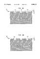
- FIG. 1illustrates an exemplary schematic cross-section of a typical metal oxide semiconductor device
- FIG. 2illustrates the semiconductor depicted in FIG. 1 with an etched film pattern
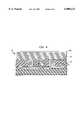
- FIG. 3Aillustrates the semiconductor depicted in FIG. 1 with a silicon film deposited over the remaining hardmask and etch stop layers;
- FIG. 3Billustrates the semiconductor depicted in FIG. 1 with silicon spacers
- FIG. 4illustrates the semiconductor depicted in FIG. 1 with contact openings
- FIG. 5illustrates the semiconductor depicted in FIG. 1 with a barrier layer and a conductive material
- FIG. 6illustrates the semiconductor depicted in FIG. 1 with a metal interconnect layer and an anti-reflective coating.
- the semiconductor 100includes a substrate 110, which may be formed from materials such as silicon, germanium, gallium arsenide or other materials known to those skilled in the art.
- the substrate 110will typically include field oxide regions 112a, 112b and doped source and drain regions 114a, 114b, both of which are formed by conventional processes.
- a gate 116 positioned on a gate oxide 118may also be formed on the substrate 110. Both the gate 116 and the gate oxide 118 are also formed by conventional processes.
- the dielectric layer 120is deposited by conventional process using well known materials such as tetraethyl orthosilicate (TEOS).
- TEOStetraethyl orthosilicate
- the dielectric layer 120is doped with phosphorous and/or boron.
- the hardmask layer 130is composed of polysilicon with a thickness of approximately 100 nm and has an etch rate at least less than 1/10 of the etch rate of the dielectric layer 120 material.
- the hardmask layer 130is composed of amorphous silicon. The use of amorphous silicon, with its wider range of operational temperature, in the hardmask layer 130 allows the deposition of the hardmask layer 130 at a lower temperature, which is typically less than 580° C.
- the hardmask layer 130is deposited on the dielectric layer 120 using chemical vapor deposition (CVD) at temperatures of approximately 400° C. to 500° C.
- CVDchemical vapor deposition
- the present inventiondoes not limit the deposition process to CVD, other deposition techniques, such as sputtering and plasma enhanced processes, may also be used to deposit the hardmask layer onto the dielectric.
- an oxide etch stop layer 140may be deposited onto the hardmask layer 130 using conventional processes.
- the etch stop layer 140is used as a barrier to prevent the etching process from penetrating past it. It should be noted that the use of the etch stop layer is not essential to the method disclosed by the present invention.
- a photoresist 150is applied typically as a thin film to the etch stop layer 140 and subsequently exposed through a mask 160 in a conventional lithographic process.
- the mask 160typically contains clear and opaque features that define an opening, such as a contact or via opening to be formed in the photoresist 150.
- contact holes or via patternare formed by plasma etch using the photoresist as a mask.
- the photoresist maskis laterally eroded during the plasma etch and the resulting pattern size becomes larger than the original dimension. Consequently, patterning the small dimension becomes more difficult to achieve.
- the deep ultraviolet (UV) photoresist used for the deep sub-micron photolithographyhas less resistance to plasma etch and results in even larger losses in critical dimension.
- the hardmask layer 130 materialis more resistant to the etching species than the photoresist 150 material and acts as a guide for etching the windows. With the use of the hardmask 130, the dimensions of the features being patterned with the mask 160 may be controlled with greater accuracy.
- the use of a hardmask as a control layerpermits the use of existing conventional stepper lithographic equipment avoiding the costs of newer and more expensive stepper lithographic equipment that employ shorter wavelengths.
- the contact opening or via patternis transferred to the photoresist 150 using conventional processes well known in the art.
- the exposed etch stop layer 140 and the hardmask layer 130are patterned using conventional processes well known in the art to form a plurality of guide openings 210 through the hardmask layer 130, which corresponds to a plurality of contact openings or vias.
- the remaining photoresist 150is then removed using conventional processes to expose the remaining hardmask layer 130.
- FIG. 3Aillustrates the semiconductor 100 depicted in FIG. 1 with a silicon film 310 deposited over the remaining hardmask and etch stop layers 130,140.
- FIG. 3Billustrates the semiconductor 100 depicted in FIG. 1 with silicon spacers 320 formed from the silicon film 310.
- a silicon film 310is deposited using conventional processes well known in the art.
- a blanket and conformal amorphous silicon film 310is deposited on the remaining etch stop layer 130 and in the guide openings 210.
- the amorphous silicon materialis then subjected to an anisotropic (directional) reactive ion etch (RIE), forming an amorphous silicon spacer 320 within the guide opening 210 hardmask pattern.
- RIEreactive ion etch
- the resultant guide openings 210are reduced by approximately twice the amorphous silicon thickness. Since the amorphous silicon deposition will typically not be isotropic, the side-wall (vertical surface) thickness will typically range from about 30% to 70% of the thickness of the amorphous silicon, as measured on a flat, i.e., horizontal, surface.
- FIG. 4illustrated is the semiconductor 100 depicted in FIG. 1 with contact openings 410 formed in the dielectric 120.
- a plurality of contact openings(generally designated as 410) are formed using conventional processes through the guide openings 210 of the hardmask layer 130.
- the spacers 320are used to control the size of the contact openings 410, allowing the use of conventional lithographic techniques to define feature sizes, e.g., contact openings or vias, of less than 0.25 ⁇ m.
- a barrier layermay be deposited in the contact openings 410 and on the hardmask layer 130 and silicon spacers 320 in a manner explained below.
- the barrier layer 510is composed of titanium (Ti) and titanium nitride (TiN).
- Tititanium
- TiNtitanium nitride
- the barrier layer 510is formed over the hardmask layer 130, silicon spacers 320, and in the contact openings 410 by first depositing a layer of Ti using a conventional process, such as physical vapor deposition. Following the deposition of the Ti layer, a second layer of TiN is deposited, also using conventional processes well known in the art, over the first Ti layer.
- a conductive material 520is deposited, using conventional processes, over the barrier layer 510.
- the conductive materialis tungsten.
- the conductive material 520is used to "plug" the contact openings 410 to provide electrical conductive paths from the source and drain regions 114a, 114b and gate 116 to a metal interconnect layer (not shown).
- the silicon spacers 320, hardmask layer 130 along with the portions of the conductive material 520 and the barrier layer 510 that do not reside in the contact openings 410are then removed.
- a chemical mechanical polishing (CMP) processis employed.
- the CMP processis initiated with the removal of the conductive material 520.
- a slurry used for polishing the conductive material 520which is typically tungsten, comprises an abrasive component and an oxidizer component.
- aluminum oxide and ferric nitrateare used as the abrasive and oxidizer, respectively, in the slurry.
- hydrogen peroxideis used as an oxidizer in the slurry.
- the conductive material 520is removed by a combination of physical, i.e., mechanical abrasion, and chemical, i.e., etching, processes.
- the slurry and the CMP's pad(not shown) are pressed onto the conductive material 520, typically at pressures of approximately 6 to 8 psi, the oxidizing component of the slurry oxidizes the conductive material 520 to form a thin layer of metal oxide. This metal oxide is then readily removed with the slurry's abrasive component. The oxidizing and removal process is repeated until the hardmask layer 130 is reached, at which time a new slurry composition is employed.
- a new slurryis required because the silicon that is used to form the hardmask and spacers will not oxidize in ferric nitrate or hydrogen peroxide.
- the new slurryis comprised of silica and a base.
- the slurryhas a pH ranging from about 7 to about 11, and for example, the base may be ammonia or potassium hydroxide.
- FIG. 6illustrated is the semiconductor 100 depicted in FIG. 1 with a metal interconnect layer 610 and an anti-reflective coating 620.
- the metal interconnect layer 610which is typically comprised of aluminum, is deposited over the dielectric layer 120 and the contact openings 410 using conventional processes well known in the art, such as physical vapor deposition.
- the anti-reflective coating 620is next deposited over the metal interconnect layer 610 also using conventional processes.
- the anti-reflective coatingis used to absorb most of the radiation that might penetrate photoresist materials in subsequent lithographic processing steps.
- the material used in the anti-reflective coating 520is TiN.
- the present inventionprovides a method of forming a contact opening in a semiconductor dielectric layer.
- the method disclosed by the present inventionwill achieve the smaller contact openings and vias required by current deep sub-micron technologies without requiring more sensitive photoresist materials and new stepper lithography equipment that uses shorter wavelengths.
- the foregoinghas outlined, rather broadly, preferred and alternative features of the present invention so that those skilled in the art may better understand the detailed description of the invention as stated herein. Moreover, those skilled in the art should appreciate that they can readily use the disclosed conception and specific embodiment as a basis for designing or modifying other structures for carrying out the same purposes of the present invention. Those skilled in the art should also realize that such equivalent constructions do not depart from the spirit and scope of the invention in its broadest form.
Landscapes
- Engineering & Computer Science (AREA)
- Physics & Mathematics (AREA)
- Condensed Matter Physics & Semiconductors (AREA)
- General Physics & Mathematics (AREA)
- Manufacturing & Machinery (AREA)
- Computer Hardware Design (AREA)
- Microelectronics & Electronic Packaging (AREA)
- Power Engineering (AREA)
- Internal Circuitry In Semiconductor Integrated Circuit Devices (AREA)
- Electrodes Of Semiconductors (AREA)
- Drying Of Semiconductors (AREA)
- Insulated Gate Type Field-Effect Transistor (AREA)
Abstract
Description
Claims (25)
Priority Applications (4)
| Application Number | Priority Date | Filing Date | Title |
|---|---|---|---|
| US08/963,687US6008123A (en) | 1997-11-04 | 1997-11-04 | Method for using a hardmask to form an opening in a semiconductor substrate |
| TW087116624ATW388960B (en) | 1997-11-04 | 1998-10-07 | Method for using a hardmask to form an opening in a semiconductor substrate |
| KR1019980047146AKR100320163B1 (en) | 1997-11-04 | 1998-11-04 | Method for using a hardmask to form an opening in a semiconductor substrate |
| JP10312637AJPH11220027A (en) | 1997-11-04 | 1998-11-04 | Method for forming opening of semiconductor substrate using hard mask |
Applications Claiming Priority (1)
| Application Number | Priority Date | Filing Date | Title |
|---|---|---|---|
| US08/963,687US6008123A (en) | 1997-11-04 | 1997-11-04 | Method for using a hardmask to form an opening in a semiconductor substrate |
Publications (1)
| Publication Number | Publication Date |
|---|---|
| US6008123Atrue US6008123A (en) | 1999-12-28 |
Family
ID=25507568
Family Applications (1)
| Application Number | Title | Priority Date | Filing Date |
|---|---|---|---|
| US08/963,687Expired - LifetimeUS6008123A (en) | 1997-11-04 | 1997-11-04 | Method for using a hardmask to form an opening in a semiconductor substrate |
Country Status (4)
| Country | Link |
|---|---|
| US (1) | US6008123A (en) |
| JP (1) | JPH11220027A (en) |
| KR (1) | KR100320163B1 (en) |
| TW (1) | TW388960B (en) |
Cited By (51)
| Publication number | Priority date | Publication date | Assignee | Title |
|---|---|---|---|---|
| US6165855A (en)* | 1998-12-04 | 2000-12-26 | Advanced Micro Devices, Inc. | Antireflective coating used in the fabrication of microcircuit structures in 0.18 micron and smaller technologies |
| US6287951B1 (en)* | 1998-12-07 | 2001-09-11 | Motorola Inc. | Process for forming a combination hardmask and antireflective layer |
| WO2002035605A1 (en)* | 2000-10-27 | 2002-05-02 | Infineon Technologies Ag | Method for forming contacts in integrated circuits |
| US20020180052A1 (en)* | 2001-06-05 | 2002-12-05 | Nace Layadi | Polish or etch stop layer |
| US20030027059A1 (en)* | 2001-07-31 | 2003-02-06 | Giorgio Schweeger | Method for producing a mask and method for fabricating a semiconductor device |
| US6610607B1 (en)* | 2000-05-25 | 2003-08-26 | International Business Machines Corporation | Method to define and tailor process limited lithographic features using a modified hard mask process |
| US6639285B1 (en) | 2000-11-15 | 2003-10-28 | Agere Systems, Inc. | Method for fabricating a semiconductor device |
| US6660456B2 (en) | 2001-06-27 | 2003-12-09 | International Business Machines Corporation | Technique for the size reduction of vias and other images in semiconductor chips |
| US20030232972A1 (en)* | 2000-12-05 | 2003-12-18 | Bowdish Katherine S. | Rationally designed antibodies |
| US20040077174A1 (en)* | 2002-10-18 | 2004-04-22 | Chartered Semiconductor Manufacturing Ltd. | Method for forming a high aspect ratio via |
| US6734488B1 (en)* | 1999-08-19 | 2004-05-11 | Renesas Technology Corp. | Semiconductor device and manufacturing method thereof |
| US20050136674A1 (en)* | 2003-12-22 | 2005-06-23 | Nanya Technology Corporation | Method for forming contact hole |
| DE102004001853B3 (en)* | 2004-01-13 | 2005-07-21 | Infineon Technologies Ag | Fabrication of connection contacts of semiconductors for future nanotechnologies including deposition of contact layer on masking layer during later back polishing stage |
| US20050158899A1 (en)* | 2002-03-18 | 2005-07-21 | Sarcos Investments Lc | Miniaturized imaging device with integrated circuit connector system |
| DE10334406B4 (en)* | 2002-08-07 | 2006-02-23 | Samsung Electronics Co., Ltd., Suwon | Method of forming a contact in a semiconductor process |
| US7105442B2 (en) | 2002-05-22 | 2006-09-12 | Applied Materials, Inc. | Ashable layers for reducing critical dimensions of integrated circuit features |
| US20060292775A1 (en)* | 2005-06-28 | 2006-12-28 | Nanya Technology Corporation | Method of manufacturing DRAM capable of avoiding bit line leakage |
| US20070178684A1 (en)* | 2006-01-31 | 2007-08-02 | Torsten Mueller | Method for producing conductor arrays on semiconductor devices |
| US20080130089A1 (en)* | 1994-05-05 | 2008-06-05 | Idc, Llc | METHOD OF FABRICATING MEMS DEVICES (SUCH AS IMod) COMPRISING USING A GAS PHASE ETCHANT TO REMOVE A LAYER |
| US20090023289A1 (en)* | 2007-07-19 | 2009-01-22 | Macronix International Co., Ltd. | Conductor removal process |
| US20090195856A1 (en)* | 2008-02-05 | 2009-08-06 | Qualcomm Mems Technologies, Inc. | Methods of reducing cd loss in a microelectromechanical device |
| US20100055902A1 (en)* | 2008-08-29 | 2010-03-04 | Kai Frohberg | Reducing critical dimensions of vias and contacts above the device level of semiconductor devices |
| US7787939B2 (en) | 2002-03-18 | 2010-08-31 | Sterling Lc | Miniaturized imaging device including utility aperture and SSID |
| US7795061B2 (en) | 2005-12-29 | 2010-09-14 | Qualcomm Mems Technologies, Inc. | Method of creating MEMS device cavities by a non-etching process |
| US20100265563A1 (en)* | 2005-08-19 | 2010-10-21 | Qualcomm Mems Technologies, Inc. | Electromechanical device configured to minimize stress-related deformation and methods for fabricating same |
| US7835074B2 (en) | 2007-06-05 | 2010-11-16 | Sterling Lc | Mini-scope for multi-directional imaging |
| US7864403B2 (en) | 2009-03-27 | 2011-01-04 | Qualcomm Mems Technologies, Inc. | Post-release adjustment of interferometric modulator reflectivity |
| US7952789B2 (en) | 2006-03-02 | 2011-05-31 | Qualcomm Mems Technologies, Inc. | MEMS devices with multi-component sacrificial layers |
| US7969659B2 (en) | 2008-01-11 | 2011-06-28 | Sterling Lc | Grin lens microscope system |
| US8064124B2 (en) | 2006-01-18 | 2011-11-22 | Qualcomm Mems Technologies, Inc. | Silicon-rich silicon nitrides as etch stops in MEMS manufacture |
| DE102010029533B3 (en)* | 2010-05-31 | 2012-02-09 | Globalfoundries Dresden Module One Limited Liability Company & Co. Kg | Selective size reduction of contact elements in a semiconductor device |
| US8115988B2 (en) | 2004-07-29 | 2012-02-14 | Qualcomm Mems Technologies, Inc. | System and method for micro-electromechanical operation of an interferometric modulator |
| US8149497B2 (en) | 2005-07-22 | 2012-04-03 | Qualcomm Mems Technologies, Inc. | Support structure for MEMS device and methods therefor |
| US8164815B2 (en) | 2007-03-21 | 2012-04-24 | Qualcomm Mems Technologies, Inc. | MEMS cavity-coating layers and methods |
| US8278726B2 (en) | 2002-09-20 | 2012-10-02 | Qualcomm Mems Technologies, Inc. | Controlling electromechanical behavior of structures within a microelectromechanical systems device |
| US8284475B2 (en) | 2007-05-11 | 2012-10-09 | Qualcomm Mems Technologies, Inc. | Methods of fabricating MEMS with spacers between plates and devices formed by same |
| US8358458B2 (en) | 2008-06-05 | 2013-01-22 | Qualcomm Mems Technologies, Inc. | Low temperature amorphous silicon sacrificial layer for controlled adhesion in MEMS devices |
| US8368124B2 (en) | 2002-09-20 | 2013-02-05 | Qualcomm Mems Technologies, Inc. | Electromechanical devices having etch barrier layers |
| US8486735B2 (en) | 2008-07-30 | 2013-07-16 | Raytheon Company | Method and device for incremental wavelength variation to analyze tissue |
| US8614768B2 (en) | 2002-03-18 | 2013-12-24 | Raytheon Company | Miniaturized imaging device including GRIN lens optically coupled to SSID |
| US8690762B2 (en) | 2008-06-18 | 2014-04-08 | Raytheon Company | Transparent endoscope head defining a focal length |
| US8717428B2 (en) | 2009-10-01 | 2014-05-06 | Raytheon Company | Light diffusion apparatus |
| US8828028B2 (en) | 2009-11-03 | 2014-09-09 | Raytheon Company | Suture device and method for closing a planar opening |
| US8928967B2 (en) | 1998-04-08 | 2015-01-06 | Qualcomm Mems Technologies, Inc. | Method and device for modulating light |
| US8971675B2 (en) | 2006-01-13 | 2015-03-03 | Qualcomm Mems Technologies, Inc. | Interconnect structure for MEMS device |
| US9060704B2 (en) | 2008-11-04 | 2015-06-23 | Sarcos Lc | Method and device for wavelength shifted imaging |
| US9110289B2 (en) | 1998-04-08 | 2015-08-18 | Qualcomm Mems Technologies, Inc. | Device for modulating light with multiple electrodes |
| US9144664B2 (en) | 2009-10-01 | 2015-09-29 | Sarcos Lc | Method and apparatus for manipulating movement of a micro-catheter |
| US9661996B2 (en) | 2009-10-01 | 2017-05-30 | Sarcos Lc | Needle delivered imaging device |
| US9984933B1 (en) | 2017-10-03 | 2018-05-29 | Globalfoundries Inc. | Silicon liner for STI CMP stop in FinFET |
| US20180269307A1 (en)* | 2017-03-15 | 2018-09-20 | Taiwan Semiconductor Manufacturing Company, Ltd. | Semiconductor Device, Method, and Tool of Manufacture |
Citations (14)
| Publication number | Priority date | Publication date | Assignee | Title |
|---|---|---|---|---|
| US5244534A (en)* | 1992-01-24 | 1993-09-14 | Micron Technology, Inc. | Two-step chemical mechanical polishing process for producing flush and protruding tungsten plugs |
| US5262352A (en)* | 1992-08-31 | 1993-11-16 | Motorola, Inc. | Method for forming an interconnection structure for conductive layers |
| US5279990A (en)* | 1990-03-02 | 1994-01-18 | Motorola, Inc. | Method of making a small geometry contact using sidewall spacers |
| US5279989A (en)* | 1992-02-29 | 1994-01-18 | Hyundai Electronics Industries Co., Ltd. | Method for forming miniature contacts of highly integrated semiconductor devices |
| US5397731A (en)* | 1993-06-30 | 1995-03-14 | Nec Corporation | Method of manufacturing semiconductor integrated circuit device |
| US5444021A (en)* | 1992-10-24 | 1995-08-22 | Hyundai Electronics Industries Co., Ltd. | Method for making a contact hole of a semiconductor device |
| US5508218A (en)* | 1993-12-28 | 1996-04-16 | Lg Semicon Co., Ltd. | Method for fabricating a semiconductor memory |
| US5525552A (en)* | 1995-06-08 | 1996-06-11 | Taiwan Semiconductor Manufacturing Company | Method for fabricating a MOSFET device with a buried contact |
| US5527423A (en)* | 1994-10-06 | 1996-06-18 | Cabot Corporation | Chemical mechanical polishing slurry for metal layers |
| US5540810A (en)* | 1992-12-11 | 1996-07-30 | Micron Technology Inc. | IC mechanical planarization process incorporating two slurry compositions for faster material removal times |
| US5562801A (en)* | 1994-04-28 | 1996-10-08 | Cypress Semiconductor Corporation | Method of etching an oxide layer |
| US5654236A (en)* | 1994-11-15 | 1997-08-05 | Nec Corporation | Method for manufacturing contact structure capable of avoiding short-circuit |
| US5677242A (en)* | 1995-01-13 | 1997-10-14 | Nec Corporation | Process of fabricating semiconductor integrated circuit device having small geometry contact by using spacer on photoresist mask |
| US5719089A (en)* | 1996-06-21 | 1998-02-17 | Vanguard International Semiconductor Corporation | Method for etching polymer-assisted reduced small contacts for ultra large scale integration semiconductor devices |
- 1997
- 1997-11-04USUS08/963,687patent/US6008123A/ennot_activeExpired - Lifetime
- 1998
- 1998-10-07TWTW087116624Apatent/TW388960B/ennot_activeIP Right Cessation
- 1998-11-04JPJP10312637Apatent/JPH11220027A/enactivePending
- 1998-11-04KRKR1019980047146Apatent/KR100320163B1/ennot_activeExpired - Fee Related
Patent Citations (14)
| Publication number | Priority date | Publication date | Assignee | Title |
|---|---|---|---|---|
| US5279990A (en)* | 1990-03-02 | 1994-01-18 | Motorola, Inc. | Method of making a small geometry contact using sidewall spacers |
| US5244534A (en)* | 1992-01-24 | 1993-09-14 | Micron Technology, Inc. | Two-step chemical mechanical polishing process for producing flush and protruding tungsten plugs |
| US5279989A (en)* | 1992-02-29 | 1994-01-18 | Hyundai Electronics Industries Co., Ltd. | Method for forming miniature contacts of highly integrated semiconductor devices |
| US5262352A (en)* | 1992-08-31 | 1993-11-16 | Motorola, Inc. | Method for forming an interconnection structure for conductive layers |
| US5444021A (en)* | 1992-10-24 | 1995-08-22 | Hyundai Electronics Industries Co., Ltd. | Method for making a contact hole of a semiconductor device |
| US5540810A (en)* | 1992-12-11 | 1996-07-30 | Micron Technology Inc. | IC mechanical planarization process incorporating two slurry compositions for faster material removal times |
| US5397731A (en)* | 1993-06-30 | 1995-03-14 | Nec Corporation | Method of manufacturing semiconductor integrated circuit device |
| US5508218A (en)* | 1993-12-28 | 1996-04-16 | Lg Semicon Co., Ltd. | Method for fabricating a semiconductor memory |
| US5562801A (en)* | 1994-04-28 | 1996-10-08 | Cypress Semiconductor Corporation | Method of etching an oxide layer |
| US5527423A (en)* | 1994-10-06 | 1996-06-18 | Cabot Corporation | Chemical mechanical polishing slurry for metal layers |
| US5654236A (en)* | 1994-11-15 | 1997-08-05 | Nec Corporation | Method for manufacturing contact structure capable of avoiding short-circuit |
| US5677242A (en)* | 1995-01-13 | 1997-10-14 | Nec Corporation | Process of fabricating semiconductor integrated circuit device having small geometry contact by using spacer on photoresist mask |
| US5525552A (en)* | 1995-06-08 | 1996-06-11 | Taiwan Semiconductor Manufacturing Company | Method for fabricating a MOSFET device with a buried contact |
| US5719089A (en)* | 1996-06-21 | 1998-02-17 | Vanguard International Semiconductor Corporation | Method for etching polymer-assisted reduced small contacts for ultra large scale integration semiconductor devices |
Non-Patent Citations (2)
| Title |
|---|
| Naokatsu Ikegami, Atsushi Yabata, Takayuki Matsui, Jun Kanamori and Yasuhiro Horiike; Characteristics of Very High Aspect Ratio Contact Hole Etching; 1996 Dry Process Symposium; pp. 147 152.* |
| Naokatsu Ikegami, Atsushi Yabata, Takayuki Matsui, Jun Kanamori and Yasuhiro Horiike; Characteristics of Very High Aspect-Ratio Contact Hole Etching; 1996 Dry Process Symposium; pp. 147-152. |
Cited By (77)
| Publication number | Priority date | Publication date | Assignee | Title |
|---|---|---|---|---|
| US8105496B2 (en) | 1994-05-05 | 2012-01-31 | Qualcomm Mems Technologies, Inc. | Method of fabricating MEMS devices (such as IMod) comprising using a gas phase etchant to remove a layer |
| US20080130089A1 (en)* | 1994-05-05 | 2008-06-05 | Idc, Llc | METHOD OF FABRICATING MEMS DEVICES (SUCH AS IMod) COMPRISING USING A GAS PHASE ETCHANT TO REMOVE A LAYER |
| US9110289B2 (en) | 1998-04-08 | 2015-08-18 | Qualcomm Mems Technologies, Inc. | Device for modulating light with multiple electrodes |
| US8928967B2 (en) | 1998-04-08 | 2015-01-06 | Qualcomm Mems Technologies, Inc. | Method and device for modulating light |
| US6165855A (en)* | 1998-12-04 | 2000-12-26 | Advanced Micro Devices, Inc. | Antireflective coating used in the fabrication of microcircuit structures in 0.18 micron and smaller technologies |
| US6287951B1 (en)* | 1998-12-07 | 2001-09-11 | Motorola Inc. | Process for forming a combination hardmask and antireflective layer |
| US6734488B1 (en)* | 1999-08-19 | 2004-05-11 | Renesas Technology Corp. | Semiconductor device and manufacturing method thereof |
| US6610607B1 (en)* | 2000-05-25 | 2003-08-26 | International Business Machines Corporation | Method to define and tailor process limited lithographic features using a modified hard mask process |
| WO2002035605A1 (en)* | 2000-10-27 | 2002-05-02 | Infineon Technologies Ag | Method for forming contacts in integrated circuits |
| US6639285B1 (en) | 2000-11-15 | 2003-10-28 | Agere Systems, Inc. | Method for fabricating a semiconductor device |
| US20030232972A1 (en)* | 2000-12-05 | 2003-12-18 | Bowdish Katherine S. | Rationally designed antibodies |
| US20020180052A1 (en)* | 2001-06-05 | 2002-12-05 | Nace Layadi | Polish or etch stop layer |
| US6660456B2 (en) | 2001-06-27 | 2003-12-09 | International Business Machines Corporation | Technique for the size reduction of vias and other images in semiconductor chips |
| DE10137575A1 (en)* | 2001-07-31 | 2003-02-27 | Infineon Technologies Ag | Process for producing a mask and process for producing a semiconductor device |
| US20030027059A1 (en)* | 2001-07-31 | 2003-02-06 | Giorgio Schweeger | Method for producing a mask and method for fabricating a semiconductor device |
| US20050158899A1 (en)* | 2002-03-18 | 2005-07-21 | Sarcos Investments Lc | Miniaturized imaging device with integrated circuit connector system |
| US8614768B2 (en) | 2002-03-18 | 2013-12-24 | Raytheon Company | Miniaturized imaging device including GRIN lens optically coupled to SSID |
| US7629659B2 (en) | 2002-03-18 | 2009-12-08 | Sterling Lc | Miniaturized imaging device with integrated circuit connector system |
| US7591780B2 (en) | 2002-03-18 | 2009-09-22 | Sterling Lc | Miniaturized imaging device with integrated circuit connector system |
| US7787939B2 (en) | 2002-03-18 | 2010-08-31 | Sterling Lc | Miniaturized imaging device including utility aperture and SSID |
| US7166537B2 (en)* | 2002-03-18 | 2007-01-23 | Sarcos Investments Lc | Miniaturized imaging device with integrated circuit connector system |
| US7105442B2 (en) | 2002-05-22 | 2006-09-12 | Applied Materials, Inc. | Ashable layers for reducing critical dimensions of integrated circuit features |
| DE10334406B4 (en)* | 2002-08-07 | 2006-02-23 | Samsung Electronics Co., Ltd., Suwon | Method of forming a contact in a semiconductor process |
| US8368124B2 (en) | 2002-09-20 | 2013-02-05 | Qualcomm Mems Technologies, Inc. | Electromechanical devices having etch barrier layers |
| US8278726B2 (en) | 2002-09-20 | 2012-10-02 | Qualcomm Mems Technologies, Inc. | Controlling electromechanical behavior of structures within a microelectromechanical systems device |
| US20040077174A1 (en)* | 2002-10-18 | 2004-04-22 | Chartered Semiconductor Manufacturing Ltd. | Method for forming a high aspect ratio via |
| SG123565A1 (en)* | 2002-10-18 | 2006-07-26 | Chartered Semiconductor Mfg | Method for forming a high aspect ratio via |
| US20050136674A1 (en)* | 2003-12-22 | 2005-06-23 | Nanya Technology Corporation | Method for forming contact hole |
| US7005374B2 (en)* | 2003-12-22 | 2006-02-28 | Nanya Technology Corporation | Method for forming contact hole |
| US7183188B2 (en) | 2004-01-13 | 2007-02-27 | Infineon Technologies Ag | Method for fabricating contact-making connections |
| US20050176239A1 (en)* | 2004-01-13 | 2005-08-11 | Infineon Technologies Ag | Method for making contact making connections |
| DE102004001853B3 (en)* | 2004-01-13 | 2005-07-21 | Infineon Technologies Ag | Fabrication of connection contacts of semiconductors for future nanotechnologies including deposition of contact layer on masking layer during later back polishing stage |
| US8115988B2 (en) | 2004-07-29 | 2012-02-14 | Qualcomm Mems Technologies, Inc. | System and method for micro-electromechanical operation of an interferometric modulator |
| US20060292775A1 (en)* | 2005-06-28 | 2006-12-28 | Nanya Technology Corporation | Method of manufacturing DRAM capable of avoiding bit line leakage |
| US8218229B2 (en) | 2005-07-22 | 2012-07-10 | Qualcomm Mems Technologies, Inc. | Support structure for MEMS device and methods therefor |
| US8149497B2 (en) | 2005-07-22 | 2012-04-03 | Qualcomm Mems Technologies, Inc. | Support structure for MEMS device and methods therefor |
| US20110058243A1 (en)* | 2005-08-19 | 2011-03-10 | Qualcomm Mems Technologies, Inc. | Methods for forming layers within a mems device using liftoff processes |
| US8298847B2 (en) | 2005-08-19 | 2012-10-30 | Qualcomm Mems Technologies, Inc. | MEMS devices having support structures with substantially vertical sidewalls and methods for fabricating the same |
| US7835093B2 (en) | 2005-08-19 | 2010-11-16 | Qualcomm Mems Technologies, Inc. | Methods for forming layers within a MEMS device using liftoff processes |
| US20100265563A1 (en)* | 2005-08-19 | 2010-10-21 | Qualcomm Mems Technologies, Inc. | Electromechanical device configured to minimize stress-related deformation and methods for fabricating same |
| US8229253B2 (en) | 2005-08-19 | 2012-07-24 | Qualcomm Mems Technologies, Inc. | Electromechanical device configured to minimize stress-related deformation and methods for fabricating same |
| US8394656B2 (en) | 2005-12-29 | 2013-03-12 | Qualcomm Mems Technologies, Inc. | Method of creating MEMS device cavities by a non-etching process |
| US7795061B2 (en) | 2005-12-29 | 2010-09-14 | Qualcomm Mems Technologies, Inc. | Method of creating MEMS device cavities by a non-etching process |
| US8971675B2 (en) | 2006-01-13 | 2015-03-03 | Qualcomm Mems Technologies, Inc. | Interconnect structure for MEMS device |
| US8064124B2 (en) | 2006-01-18 | 2011-11-22 | Qualcomm Mems Technologies, Inc. | Silicon-rich silicon nitrides as etch stops in MEMS manufacture |
| US20070178684A1 (en)* | 2006-01-31 | 2007-08-02 | Torsten Mueller | Method for producing conductor arrays on semiconductor devices |
| US7952789B2 (en) | 2006-03-02 | 2011-05-31 | Qualcomm Mems Technologies, Inc. | MEMS devices with multi-component sacrificial layers |
| US8164815B2 (en) | 2007-03-21 | 2012-04-24 | Qualcomm Mems Technologies, Inc. | MEMS cavity-coating layers and methods |
| US8284475B2 (en) | 2007-05-11 | 2012-10-09 | Qualcomm Mems Technologies, Inc. | Methods of fabricating MEMS with spacers between plates and devices formed by same |
| US8830557B2 (en) | 2007-05-11 | 2014-09-09 | Qualcomm Mems Technologies, Inc. | Methods of fabricating MEMS with spacers between plates and devices formed by same |
| US8358462B2 (en) | 2007-06-05 | 2013-01-22 | Jacobsen Stephen C | Mini-scope for multi-directional imaging |
| US7835074B2 (en) | 2007-06-05 | 2010-11-16 | Sterling Lc | Mini-scope for multi-directional imaging |
| US8288280B2 (en)* | 2007-07-19 | 2012-10-16 | Macronix International Co., Ltd. | Conductor removal process |
| US20090023289A1 (en)* | 2007-07-19 | 2009-01-22 | Macronix International Co., Ltd. | Conductor removal process |
| US7969659B2 (en) | 2008-01-11 | 2011-06-28 | Sterling Lc | Grin lens microscope system |
| US7863079B2 (en)* | 2008-02-05 | 2011-01-04 | Qualcomm Mems Technologies, Inc. | Methods of reducing CD loss in a microelectromechanical device |
| US20090195856A1 (en)* | 2008-02-05 | 2009-08-06 | Qualcomm Mems Technologies, Inc. | Methods of reducing cd loss in a microelectromechanical device |
| US8358458B2 (en) | 2008-06-05 | 2013-01-22 | Qualcomm Mems Technologies, Inc. | Low temperature amorphous silicon sacrificial layer for controlled adhesion in MEMS devices |
| US8690762B2 (en) | 2008-06-18 | 2014-04-08 | Raytheon Company | Transparent endoscope head defining a focal length |
| US9521946B2 (en) | 2008-06-18 | 2016-12-20 | Sarcos Lc | Transparent endoscope head defining a focal length |
| US9259142B2 (en) | 2008-07-30 | 2016-02-16 | Sarcos Lc | Method and device for incremental wavelength variation to analyze tissue |
| US8486735B2 (en) | 2008-07-30 | 2013-07-16 | Raytheon Company | Method and device for incremental wavelength variation to analyze tissue |
| DE102008045036B4 (en)* | 2008-08-29 | 2011-06-22 | GLOBALFOUNDRIES Dresden Module One Ltd. Liability Company & Co. KG, 01109 | Reducing critical dimensions of vias and contacts above the device level of semiconductor devices |
| US20100055902A1 (en)* | 2008-08-29 | 2010-03-04 | Kai Frohberg | Reducing critical dimensions of vias and contacts above the device level of semiconductor devices |
| US9717418B2 (en) | 2008-11-04 | 2017-08-01 | Sarcos Lc | Method and device for wavelength shifted imaging |
| US9060704B2 (en) | 2008-11-04 | 2015-06-23 | Sarcos Lc | Method and device for wavelength shifted imaging |
| US7864403B2 (en) | 2009-03-27 | 2011-01-04 | Qualcomm Mems Technologies, Inc. | Post-release adjustment of interferometric modulator reflectivity |
| US8717428B2 (en) | 2009-10-01 | 2014-05-06 | Raytheon Company | Light diffusion apparatus |
| US9144664B2 (en) | 2009-10-01 | 2015-09-29 | Sarcos Lc | Method and apparatus for manipulating movement of a micro-catheter |
| US9661996B2 (en) | 2009-10-01 | 2017-05-30 | Sarcos Lc | Needle delivered imaging device |
| US8828028B2 (en) | 2009-11-03 | 2014-09-09 | Raytheon Company | Suture device and method for closing a planar opening |
| US8536050B2 (en) | 2010-05-31 | 2013-09-17 | Globalfoundries Inc. | Selective shrinkage of contact elements in a semiconductor device |
| DE102010029533B3 (en)* | 2010-05-31 | 2012-02-09 | Globalfoundries Dresden Module One Limited Liability Company & Co. Kg | Selective size reduction of contact elements in a semiconductor device |
| US20180269307A1 (en)* | 2017-03-15 | 2018-09-20 | Taiwan Semiconductor Manufacturing Company, Ltd. | Semiconductor Device, Method, and Tool of Manufacture |
| US10804370B2 (en)* | 2017-03-15 | 2020-10-13 | Taiwan Semiconductor Manufacturing Company, Ltd. | Semiconductor device, method, and tool of manufacture |
| US11621342B2 (en) | 2017-03-15 | 2023-04-04 | Taiwan Semiconductor Manufacturing Company, Ltd. | Semiconductor device, method, and tool of manufacture |
| US9984933B1 (en) | 2017-10-03 | 2018-05-29 | Globalfoundries Inc. | Silicon liner for STI CMP stop in FinFET |
Also Published As
| Publication number | Publication date |
|---|---|
| JPH11220027A (en) | 1999-08-10 |
| TW388960B (en) | 2000-05-01 |
| KR100320163B1 (en) | 2002-02-19 |
| KR19990044999A (en) | 1999-06-25 |
Similar Documents
| Publication | Publication Date | Title |
|---|---|---|
| US6008123A (en) | Method for using a hardmask to form an opening in a semiconductor substrate | |
| KR100655536B1 (en) | Silylation method to reduce minimum linewidth loss and resist loss | |
| US7354847B2 (en) | Method of trimming technology | |
| US6136679A (en) | Gate micro-patterning process | |
| US5447874A (en) | Method for making a semiconductor device comprising a dual metal gate using a chemical mechanical polish | |
| US5310626A (en) | Method for forming a patterned layer using dielectric materials as a light-sensitive material | |
| US6818141B1 (en) | Application of the CVD bilayer ARC as a hard mask for definition of the subresolution trench features between polysilicon wordlines | |
| US20130175658A1 (en) | Tone inversion with partial underlayer etch for semiconductor device formation | |
| US20030219683A1 (en) | Low temperature resist trimming process | |
| JPH08255752A (en) | Semiconductor element with low reflectance coating and its preparation | |
| EP0686999B1 (en) | Pattern formation in the fabrication of microelectronic devices | |
| KR101164690B1 (en) | A semiconductor device having an organic anti-reflective coatingarc and method therefor | |
| US6037276A (en) | Method for improving patterning of a conductive layer in an integrated circuit | |
| US20080020327A1 (en) | Method of formation of a damascene structure | |
| KR100281213B1 (en) | Method for manufacturing semiconductor device | |
| US20050118531A1 (en) | Method for controlling critical dimension by utilizing resist sidewall protection | |
| US6602794B1 (en) | Silylation process for forming contacts | |
| US6281115B1 (en) | Sidewall protection for a via hole formed in a photosensitive, low dielectric constant layer | |
| US6133128A (en) | Method for patterning polysilicon gate layer based on a photodefinable hard mask process | |
| US5902133A (en) | Method of forming a narrow polysilicon gate with i-line lithography | |
| JP2001326173A (en) | Pattern formation method | |
| US7087533B2 (en) | Method for fabricating semiconductor device | |
| US7169711B1 (en) | Method of using carbon spacers for critical dimension (CD) reduction | |
| US20020137331A1 (en) | Method of forming contact holes of reduced dimensions by using reverse-transcription process | |
| CN112687528B (en) | Semiconductor structure and forming method thereof |
Legal Events
| Date | Code | Title | Description |
|---|---|---|---|
| AS | Assignment | Owner name:LUCENT TECHNOLOGIES, INC., NEW JERSEY Free format text:ASSIGNMENT OF ASSIGNORS INTEREST;ASSIGNORS:KOOK, TAEHO;MAURY, ALVARO;STEINER, KURT G.;AND OTHERS;REEL/FRAME:008804/0469 Effective date:19971030 | |
| FEPP | Fee payment procedure | Free format text:PAYOR NUMBER ASSIGNED (ORIGINAL EVENT CODE: ASPN); ENTITY STATUS OF PATENT OWNER: LARGE ENTITY | |
| STCF | Information on status: patent grant | Free format text:PATENTED CASE | |
| FEPP | Fee payment procedure | Free format text:PAYOR NUMBER ASSIGNED (ORIGINAL EVENT CODE: ASPN); ENTITY STATUS OF PATENT OWNER: LARGE ENTITY Free format text:PAYER NUMBER DE-ASSIGNED (ORIGINAL EVENT CODE: RMPN); ENTITY STATUS OF PATENT OWNER: LARGE ENTITY | |
| FPAY | Fee payment | Year of fee payment:4 | |
| REMI | Maintenance fee reminder mailed | ||
| FPAY | Fee payment | Year of fee payment:8 | |
| FPAY | Fee payment | Year of fee payment:12 | |
| AS | Assignment | Owner name:DEUTSCHE BANK AG NEW YORK BRANCH, AS COLLATERAL AG Free format text:PATENT SECURITY AGREEMENT;ASSIGNORS:LSI CORPORATION;AGERE SYSTEMS LLC;REEL/FRAME:032856/0031 Effective date:20140506 | |
| AS | Assignment | Owner name:AVAGO TECHNOLOGIES GENERAL IP (SINGAPORE) PTE. LTD Free format text:ASSIGNMENT OF ASSIGNORS INTEREST;ASSIGNOR:AGERE SYSTEMS LLC;REEL/FRAME:035365/0634 Effective date:20140804 | |
| AS | Assignment | Owner name:AGERE SYSTEMS LLC, PENNSYLVANIA Free format text:TERMINATION AND RELEASE OF SECURITY INTEREST IN PATENT RIGHTS (RELEASES RF 032856-0031);ASSIGNOR:DEUTSCHE BANK AG NEW YORK BRANCH, AS COLLATERAL AGENT;REEL/FRAME:037684/0039 Effective date:20160201 Owner name:LSI CORPORATION, CALIFORNIA Free format text:TERMINATION AND RELEASE OF SECURITY INTEREST IN PATENT RIGHTS (RELEASES RF 032856-0031);ASSIGNOR:DEUTSCHE BANK AG NEW YORK BRANCH, AS COLLATERAL AGENT;REEL/FRAME:037684/0039 Effective date:20160201 | |
| AS | Assignment | Owner name:BANK OF AMERICA, N.A., AS COLLATERAL AGENT, NORTH CAROLINA Free format text:PATENT SECURITY AGREEMENT;ASSIGNOR:AVAGO TECHNOLOGIES GENERAL IP (SINGAPORE) PTE. LTD.;REEL/FRAME:037808/0001 Effective date:20160201 Owner name:BANK OF AMERICA, N.A., AS COLLATERAL AGENT, NORTH Free format text:PATENT SECURITY AGREEMENT;ASSIGNOR:AVAGO TECHNOLOGIES GENERAL IP (SINGAPORE) PTE. LTD.;REEL/FRAME:037808/0001 Effective date:20160201 | |
| AS | Assignment | Owner name:AVAGO TECHNOLOGIES GENERAL IP (SINGAPORE) PTE. LTD., SINGAPORE Free format text:TERMINATION AND RELEASE OF SECURITY INTEREST IN PATENTS;ASSIGNOR:BANK OF AMERICA, N.A., AS COLLATERAL AGENT;REEL/FRAME:041710/0001 Effective date:20170119 Owner name:AVAGO TECHNOLOGIES GENERAL IP (SINGAPORE) PTE. LTD Free format text:TERMINATION AND RELEASE OF SECURITY INTEREST IN PATENTS;ASSIGNOR:BANK OF AMERICA, N.A., AS COLLATERAL AGENT;REEL/FRAME:041710/0001 Effective date:20170119 | |
| AS | Assignment | Owner name:BELL SEMICONDUCTOR, LLC, ILLINOIS Free format text:ASSIGNMENT OF ASSIGNORS INTEREST;ASSIGNORS:AVAGO TECHNOLOGIES GENERAL IP (SINGAPORE) PTE. LTD.;BROADCOM CORPORATION;REEL/FRAME:044886/0608 Effective date:20171208 | |
| AS | Assignment | Owner name:CORTLAND CAPITAL MARKET SERVICES LLC, AS COLLATERA Free format text:SECURITY INTEREST;ASSIGNORS:HILCO PATENT ACQUISITION 56, LLC;BELL SEMICONDUCTOR, LLC;BELL NORTHERN RESEARCH, LLC;REEL/FRAME:045216/0020 Effective date:20180124 | |
| AS | Assignment | Owner name:BELL NORTHERN RESEARCH, LLC, ILLINOIS Free format text:RELEASE BY SECURED PARTY;ASSIGNOR:CORTLAND CAPITAL MARKET SERVICES LLC;REEL/FRAME:059720/0719 Effective date:20220401 Owner name:BELL SEMICONDUCTOR, LLC, ILLINOIS Free format text:RELEASE BY SECURED PARTY;ASSIGNOR:CORTLAND CAPITAL MARKET SERVICES LLC;REEL/FRAME:059720/0719 Effective date:20220401 Owner name:HILCO PATENT ACQUISITION 56, LLC, ILLINOIS Free format text:RELEASE BY SECURED PARTY;ASSIGNOR:CORTLAND CAPITAL MARKET SERVICES LLC;REEL/FRAME:059720/0719 Effective date:20220401 |