US6007635A - Platform for supporting a semiconductor substrate and method of supporting a substrate during rapid high temperature processing - Google Patents
Platform for supporting a semiconductor substrate and method of supporting a substrate during rapid high temperature processingDownload PDFInfo
- Publication number
- US6007635A US6007635AUS08/979,604US97960497AUS6007635AUS 6007635 AUS6007635 AUS 6007635AUS 97960497 AUS97960497 AUS 97960497AUS 6007635 AUS6007635 AUS 6007635A
- Authority
- US
- United States
- Prior art keywords
- platform
- substrate
- recessed
- support surface
- housing
- Prior art date
- Legal status (The legal status is an assumption and is not a legal conclusion. Google has not performed a legal analysis and makes no representation as to the accuracy of the status listed.)
- Expired - Lifetime
Links
- 239000000758substrateSubstances0.000titleclaimsabstractdescription177
- 239000004065semiconductorSubstances0.000titleclaimsdescription32
- 238000000034methodMethods0.000titleclaimsdescription18
- 230000008021depositionEffects0.000claimsabstractdescription6
- HBMJWWWQQXIZIP-UHFFFAOYSA-Nsilicon carbideChemical compound[Si+]#[C-]HBMJWWWQQXIZIP-UHFFFAOYSA-N0.000claimsdescription7
- 229910010271silicon carbideInorganic materials0.000claimsdescription7
- OKTJSMMVPCPJKN-UHFFFAOYSA-NCarbonChemical compound[C]OKTJSMMVPCPJKN-UHFFFAOYSA-N0.000claimsdescription6
- 229910002804graphiteInorganic materials0.000claimsdescription6
- 239000010439graphiteSubstances0.000claimsdescription6
- 239000000463materialSubstances0.000claimsdescription6
- 230000008878couplingEffects0.000claimsdescription5
- 238000010168coupling processMethods0.000claimsdescription5
- 238000005859coupling reactionMethods0.000claimsdescription5
- MCMNRKCIXSYSNV-UHFFFAOYSA-NZirconium dioxideChemical compoundO=[Zr]=OMCMNRKCIXSYSNV-UHFFFAOYSA-N0.000claimsdescription4
- 239000010453quartzSubstances0.000claimsdescription4
- VYPSYNLAJGMNEJ-UHFFFAOYSA-Nsilicon dioxideInorganic materialsO=[Si]=OVYPSYNLAJGMNEJ-UHFFFAOYSA-N0.000claimsdescription4
- 230000004888barrier functionEffects0.000claimsdescription3
- 230000004907fluxEffects0.000claimsdescription3
- 229910000831SteelInorganic materials0.000claimsdescription2
- 229910052782aluminiumInorganic materials0.000claimsdescription2
- XAGFODPZIPBFFR-UHFFFAOYSA-NaluminiumChemical compound[Al]XAGFODPZIPBFFR-UHFFFAOYSA-N0.000claimsdescription2
- PNEYBMLMFCGWSK-UHFFFAOYSA-Naluminium oxideInorganic materials[O-2].[O-2].[O-2].[Al+3].[Al+3]PNEYBMLMFCGWSK-UHFFFAOYSA-N0.000claimsdescription2
- 239000010959steelSubstances0.000claimsdescription2
- 239000007789gasSubstances0.000description19
- 238000010438heat treatmentMethods0.000description15
- 235000012431wafersNutrition0.000description11
- 238000001816coolingMethods0.000description6
- 238000002347injectionMethods0.000description6
- 239000007924injectionSubstances0.000description6
- 238000005229chemical vapour depositionMethods0.000description5
- 238000004519manufacturing processMethods0.000description5
- 230000008569processEffects0.000description5
- 238000000151depositionMethods0.000description4
- 230000002093peripheral effectEffects0.000description4
- 238000000227grindingMethods0.000description3
- 238000003754machiningMethods0.000description3
- XKRFYHLGVUSROY-UHFFFAOYSA-NArgonChemical compound[Ar]XKRFYHLGVUSROY-UHFFFAOYSA-N0.000description2
- IJGRMHOSHXDMSA-UHFFFAOYSA-NAtomic nitrogenChemical compoundN#NIJGRMHOSHXDMSA-UHFFFAOYSA-N0.000description2
- XUIMIQQOPSSXEZ-UHFFFAOYSA-NSiliconChemical compound[Si]XUIMIQQOPSSXEZ-UHFFFAOYSA-N0.000description2
- 238000000137annealingMethods0.000description2
- 230000005540biological transmissionEffects0.000description2
- 239000002131composite materialSubstances0.000description2
- 239000010408filmSubstances0.000description2
- 239000011261inert gasSubstances0.000description2
- 238000005259measurementMethods0.000description2
- 229910052710siliconInorganic materials0.000description2
- 239000010703siliconSubstances0.000description2
- 239000010409thin filmSubstances0.000description2
- 238000000427thin-film depositionMethods0.000description2
- 230000001154acute effectEffects0.000description1
- 229910052786argonInorganic materials0.000description1
- 239000000919ceramicSubstances0.000description1
- 238000005234chemical depositionMethods0.000description1
- 238000005516engineering processMethods0.000description1
- 238000005530etchingMethods0.000description1
- 229910052736halogenInorganic materials0.000description1
- 239000001307heliumSubstances0.000description1
- 229910052734heliumInorganic materials0.000description1
- SWQJXJOGLNCZEY-UHFFFAOYSA-Nhelium atomChemical compound[He]SWQJXJOGLNCZEY-UHFFFAOYSA-N0.000description1
- 230000001771impaired effectEffects0.000description1
- 230000001788irregularEffects0.000description1
- 230000007246mechanismEffects0.000description1
- 229910052751metalInorganic materials0.000description1
- 239000002184metalSubstances0.000description1
- 150000004767nitridesChemical class0.000description1
- 229910052757nitrogenInorganic materials0.000description1
- 230000035515penetrationEffects0.000description1
- 229910021420polycrystalline siliconInorganic materials0.000description1
- 229920005591polysiliconPolymers0.000description1
- 230000005855radiationEffects0.000description1
- 230000002787reinforcementEffects0.000description1
- 238000004513sizingMethods0.000description1
- WFKWXMTUELFFGS-UHFFFAOYSA-NtungstenChemical compound[W]WFKWXMTUELFFGS-UHFFFAOYSA-N0.000description1
- 229910052721tungstenInorganic materials0.000description1
- 239000010937tungstenSubstances0.000description1
- WQJQOUPTWCFRMM-UHFFFAOYSA-Ntungsten disilicideChemical compound[Si]#[W]#[Si]WQJQOUPTWCFRMM-UHFFFAOYSA-N0.000description1
- 229910021342tungsten silicideInorganic materials0.000description1
Images


Classifications
- H—ELECTRICITY
- H01—ELECTRIC ELEMENTS
- H01L—SEMICONDUCTOR DEVICES NOT COVERED BY CLASS H10
- H01L21/00—Processes or apparatus adapted for the manufacture or treatment of semiconductor or solid state devices or of parts thereof
- H01L21/67—Apparatus specially adapted for handling semiconductor or electric solid state devices during manufacture or treatment thereof; Apparatus specially adapted for handling wafers during manufacture or treatment of semiconductor or electric solid state devices or components ; Apparatus not specifically provided for elsewhere
- H01L21/683—Apparatus specially adapted for handling semiconductor or electric solid state devices during manufacture or treatment thereof; Apparatus specially adapted for handling wafers during manufacture or treatment of semiconductor or electric solid state devices or components ; Apparatus not specifically provided for elsewhere for supporting or gripping
- H01L21/687—Apparatus specially adapted for handling semiconductor or electric solid state devices during manufacture or treatment thereof; Apparatus specially adapted for handling wafers during manufacture or treatment of semiconductor or electric solid state devices or components ; Apparatus not specifically provided for elsewhere for supporting or gripping using mechanical means, e.g. chucks, clamps or pinches
- H01L21/68714—Apparatus specially adapted for handling semiconductor or electric solid state devices during manufacture or treatment thereof; Apparatus specially adapted for handling wafers during manufacture or treatment of semiconductor or electric solid state devices or components ; Apparatus not specifically provided for elsewhere for supporting or gripping using mechanical means, e.g. chucks, clamps or pinches the wafers being placed on a susceptor, stage or support
- H01L21/68785—Apparatus specially adapted for handling semiconductor or electric solid state devices during manufacture or treatment thereof; Apparatus specially adapted for handling wafers during manufacture or treatment of semiconductor or electric solid state devices or components ; Apparatus not specifically provided for elsewhere for supporting or gripping using mechanical means, e.g. chucks, clamps or pinches the wafers being placed on a susceptor, stage or support characterised by the mechanical construction of the susceptor, stage or support
- C—CHEMISTRY; METALLURGY
- C23—COATING METALLIC MATERIAL; COATING MATERIAL WITH METALLIC MATERIAL; CHEMICAL SURFACE TREATMENT; DIFFUSION TREATMENT OF METALLIC MATERIAL; COATING BY VACUUM EVAPORATION, BY SPUTTERING, BY ION IMPLANTATION OR BY CHEMICAL VAPOUR DEPOSITION, IN GENERAL; INHIBITING CORROSION OF METALLIC MATERIAL OR INCRUSTATION IN GENERAL
- C23C—COATING METALLIC MATERIAL; COATING MATERIAL WITH METALLIC MATERIAL; SURFACE TREATMENT OF METALLIC MATERIAL BY DIFFUSION INTO THE SURFACE, BY CHEMICAL CONVERSION OR SUBSTITUTION; COATING BY VACUUM EVAPORATION, BY SPUTTERING, BY ION IMPLANTATION OR BY CHEMICAL VAPOUR DEPOSITION, IN GENERAL
- C23C16/00—Chemical coating by decomposition of gaseous compounds, without leaving reaction products of surface material in the coating, i.e. chemical vapour deposition [CVD] processes
- C23C16/44—Chemical coating by decomposition of gaseous compounds, without leaving reaction products of surface material in the coating, i.e. chemical vapour deposition [CVD] processes characterised by the method of coating
- C23C16/458—Chemical coating by decomposition of gaseous compounds, without leaving reaction products of surface material in the coating, i.e. chemical vapour deposition [CVD] processes characterised by the method of coating characterised by the method used for supporting substrates in the reaction chamber
- C23C16/4582—Rigid and flat substrates, e.g. plates or discs
- C23C16/4583—Rigid and flat substrates, e.g. plates or discs the substrate being supported substantially horizontally
- C23C16/4584—Rigid and flat substrates, e.g. plates or discs the substrate being supported substantially horizontally the substrate being rotated
- C—CHEMISTRY; METALLURGY
- C30—CRYSTAL GROWTH
- C30B—SINGLE-CRYSTAL GROWTH; UNIDIRECTIONAL SOLIDIFICATION OF EUTECTIC MATERIAL OR UNIDIRECTIONAL DEMIXING OF EUTECTOID MATERIAL; REFINING BY ZONE-MELTING OF MATERIAL; PRODUCTION OF A HOMOGENEOUS POLYCRYSTALLINE MATERIAL WITH DEFINED STRUCTURE; SINGLE CRYSTALS OR HOMOGENEOUS POLYCRYSTALLINE MATERIAL WITH DEFINED STRUCTURE; AFTER-TREATMENT OF SINGLE CRYSTALS OR A HOMOGENEOUS POLYCRYSTALLINE MATERIAL WITH DEFINED STRUCTURE; APPARATUS THEREFOR
- C30B25/00—Single-crystal growth by chemical reaction of reactive gases, e.g. chemical vapour-deposition growth
- C30B25/02—Epitaxial-layer growth
- C30B25/12—Substrate holders or susceptors
- C—CHEMISTRY; METALLURGY
- C30—CRYSTAL GROWTH
- C30B—SINGLE-CRYSTAL GROWTH; UNIDIRECTIONAL SOLIDIFICATION OF EUTECTIC MATERIAL OR UNIDIRECTIONAL DEMIXING OF EUTECTOID MATERIAL; REFINING BY ZONE-MELTING OF MATERIAL; PRODUCTION OF A HOMOGENEOUS POLYCRYSTALLINE MATERIAL WITH DEFINED STRUCTURE; SINGLE CRYSTALS OR HOMOGENEOUS POLYCRYSTALLINE MATERIAL WITH DEFINED STRUCTURE; AFTER-TREATMENT OF SINGLE CRYSTALS OR A HOMOGENEOUS POLYCRYSTALLINE MATERIAL WITH DEFINED STRUCTURE; APPARATUS THEREFOR
- C30B31/00—Diffusion or doping processes for single crystals or homogeneous polycrystalline material with defined structure; Apparatus therefor
- C30B31/06—Diffusion or doping processes for single crystals or homogeneous polycrystalline material with defined structure; Apparatus therefor by contacting with diffusion material in the gaseous state
- C30B31/14—Substrate holders or susceptors
- H—ELECTRICITY
- H01—ELECTRIC ELEMENTS
- H01L—SEMICONDUCTOR DEVICES NOT COVERED BY CLASS H10
- H01L21/00—Processes or apparatus adapted for the manufacture or treatment of semiconductor or solid state devices or of parts thereof
- H01L21/67—Apparatus specially adapted for handling semiconductor or electric solid state devices during manufacture or treatment thereof; Apparatus specially adapted for handling wafers during manufacture or treatment of semiconductor or electric solid state devices or components ; Apparatus not specifically provided for elsewhere
- H01L21/67005—Apparatus not specifically provided for elsewhere
- H01L21/67011—Apparatus for manufacture or treatment
- H01L21/67098—Apparatus for thermal treatment
- H01L21/67115—Apparatus for thermal treatment mainly by radiation
Definitions
- the present inventionrelates to a platform for a processing chamber and, more particularly, to a platform for supporting semiconductor substrates during thermal processing and chemical deposition of thin film applications, for example, during film deposition, oxide growth, etching, and thermal annealing.
- a chemical vapor deposition reactorwhich includes a heater platform which provides uniform support to the wafer.
- the platformincludes a recessed circular well for holding the semiconductor wafer therein. While the size of the platform can be increased to accommodate larger substrates, as the dimensions of the platform increase, the thickness necessarily increases in order to provide sufficient structural capacity. However, as the thickness of the platform increases the heat transfer rate reduces. Hence, the rapid processing of the semiconductor substrates may be impaired because of the reduced heat transfer rates.
- a platformwhich can support a semiconductor substrate during thermal processing in a manner to limit depositions of processing gases to a single side--the device side--of the substrate and permit rapid heating of the substrate. Furthermore, there is a need for a platform which has sufficient structural integrity to support large semiconductor substrates, on the order of up to 300 mm or greater, without impeding the heat transfer from the heater source to the substrate.
- the platform of the present inventionprovides numerous advantages over prior known platforms.
- the platformprovides a support for a semiconductor substrate during thermal processing which permits the non-device side of the substrate to be isolated from the processing chamber in a conventional processing reactor.
- the platformpermits the heat transfer from the heater assembly of the reactor to the substrate to be maximized and, yet, provides a platform which can support semiconductor substrates on the order of 300 mm in diameter or greater.
- the platformfurther provides for at least one stacking member which is unrestrained from thermal radial expansion during the thermal processing of the semiconductor substrate.
- the platform of the present inventionmay include a non-device side shower head injection system for cooling or heating the substrate.
- a platform for supporting a semiconductor substrate during processing in a processing chamberincludes a first member and a second member.
- the first memberdefines a first support surface which is adapted to support the substrate thereon.
- the second memberincludes a second support surface and a third support surface. The first member is supported by the second support surface of the second member, and the third support surface of the second member is adapted to be supported in the processing chamber.
- the first memberis rotatably coupled to the second member. In this manner, when the semiconductor substrate is processed in a processing chamber with a rotating platform, the first and second members rotate in unison.
- the first membercomprises a disc member with a recessed surface defining the first support surface.
- the disc memberincludes an annular surface which extends around the recessed surface.
- the first support surfaceis adapted to support the substrate so that the upper surface of the substrate is substantially flush with the annular surface of the disc member.
- one memberincludes at least one positioning pin and the other member includes a positioning pin receiving structure for releasably rotatably coupling the first member and the second member together.
- the positioning pin receiving structurepreferably comprises a slotted aperture, which permits unrestrained relative radial thermal expansion of the first and second members during the thermal processing of the substrate.
- the first support surface of the first membercomprises a foraminous surface, which is adapted to permit the flow of gases through the first support surface for heating or cooling of the substrate.
- the first memberincludes a slot, which extends transversely through at least a portion of the first member, whereby the first member exhibits reduced hoop stresses during the thermal processing of the substrate.
- the slotcomprises a radial transverse slot which extends from a central portion of the first support surface to a free edge of the first member.
- a reactor for processing a substratein another form of the invention, includes a first housing defining a processing chamber and a second housing which is rotatably supported in the first housing.
- the substrateis supported on the second housing by a platform.
- the platformincludes a first member defining a first support surface adapted to support the substrate thereon and a second member, which includes a second support surface and a third support surface.
- the first memberis supported by the second support surface of the second member.
- the third support surface of the second memberis supported by the second housing.
- the reactorfurther includes a heater, which is adapted to heat the substrate, and is supported by the first housing and enclosed in the second housing.
- At least one gas injectoris provided which injects at least one gas into the processing chamber for deposition onto the substrate.
- a method of supporting a semiconductor substrate during processingincludes supporting a substrate on a first member and supporting the first member on a second member.
- the second memberis supported in a processing chamber.
- the processing chamber, the first member, and the second memberare adapted to permit unrestrained radial thermal expansion of the substrate, the first member, and the second member during thermal processing of the substrate.
- a platform for supporting a semiconductor substrate during processingincludes a central opening, a first side with a generally planar recessed surface and a second side configured for being supported by a rotatable housing in a processing chamber.
- the recessed surfaceis configured to support the substrate thereon and to permit unrestrained thermal expansion of the substrate.
- the annular memberis configured to be supported in the processing chamber in a radially unrestrained manner to permit radial thermal expansion of the platform.
- the platformfurther includes a coupler, which is positioned on the second side of the platform for rotatably coupling the annular member to the rotatable housing and is configured to permit unrestrained thermal expansion of the platform during thermal processing.
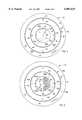
- FIG. 1is an exploded segmented cross-sectional view of the platform of the present invention
- FIG. 2is a segmented plan view of the platform with a semiconductor wafer supported thereon;
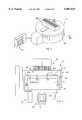
- FIG. 3is a perspective view of a suitable chemical vapor deposition reactor employing the platform of FIG. 1;
- FIG. 4is a schematic sectional view taken along line IV--IV of FIG. 3;
- FIG. 5is a plan view of a second embodiment of the platform
- FIG. 6is a plan view of a third embodiment of the platform.
- FIG. 7is sectional view taken along line VII--VII of FIG. 6.
- FIG. 8is an exploded segmented cross-sectional view of a fourth embodiment of the platform.
- FIG. 9is a top plan view of the platform in FIG. 8.
- platform 10comprises a single wafer processing platform that is suitable for supporting a semiconductor substrate 12 during various fabrication processes, such as thermal annealing, thermal reflow of boro-phosphorous gases, and chemical vapor deposition of thin film applications, including high temperature oxide, low temperature oxide, high temperature nitride, doped and undoped polysilicon, silicon epitaxial and tungsten metal and tungsten silicide films, in the fabrication of semiconductor devices.
- platform 10comprises a composite platform which is especially suited for use in a chemical vapor deposition reactor, such as reactor 13 shown in FIGS. 3 and 4, which is described in more detail in co-pending application Ser. No. 08/911,638 entitled REACTOR AND METHOD OF PROCESSING A SEMICONDUCTOR SUBSTRATE filed on Aug. 15, 1997, by Imad Mahawili, now U.S. Pat. No. 5,814,365, which is incorporated by reference in its entirety herein. But it should be understood that platform 10 may be used in other processing reactors.
- platform 10includes a first member 14, which provides a generally planar support surface 16 for substrate 12.
- Support surface 16is sized to permit unrestrained radial expansion of substrate 12 and, furthermore, is recessed to support substrate 12 substantially flush with an upper surface 14a of first member 14.
- Platform 10also includes a second member 18, which provides a support surface 20 for first member 14.
- Support surface 20is sized to permit radial expansion of first member 14 and recessed to support first member 14 and substrate 12 substantially flush with an upper surface 18a of second member 18. In this manner, processing gases may flow across substrate 12 unimpeded by an irregular surface topology created by the edges of substrate 12 or first member 14.
- heater assembly 24which provides heat to substrate 12 through platform 10 during processing.
- Heater assembly 24is designed to deliver radiant heat to substrate 12 through platform 10 in a manner such that the temperature in the substrate is substantially uniform.
- heater assembly 24includes an array of heating elements such as linear tungsten-halogen lamps (not shown), which emit peak radiation at 0.95 microns and are layered to form a plurality of heating zones, which provide a concentrated heating profile with a greater amount of heat being applied to the outer perimeter of the substrate than the center of the substrate.
- heater assembly 24For further details of heater assembly 24, reference is made to co-pending U.S. Patent application entitled RAPID THERMAL PROCESSING HEATER TECHNOLOGY AND METHOD OF USE, filed on Dec. 4, 1996, Ser. No. 08/759,559, which is incorporated herein by reference in its entirety. It should be understood that other heaters may be used to heat substrate 12; however, heater assembly 24 preferably delivers heat to substrate 12 in a substantially uniform manner.
- heater assembly 24is enclosed and, preferably, sealed in heater housing 22, which is mounted on a rotatable base 26 of reactor housing 28.
- Heater housing 22is made from a suitable material, such as a ceramic, graphite, or, more preferably, from silicon carbide coated graphite.
- Heater assembly 24, heater housing 22, and rotatable base 26are enclosed and vacuum sealed in outer, reactor housing 28 and are supported on a base wall 30 of reactor housing 28.
- Base 26 and housing 22are rotatably supported on base wall 30 of housing 28 and are rotated, preferably, using a conventional magnetically coupled drive 32 or other suitable driving devices, which can impart rotation to base 26 through a vacuum seal.
- Platform 10comprises a suitable material, such as quartz, pure silicon carbide, silicon carbide coated graphite, zirconia, alumina, aluminum, steel, or the like.
- platform 10when processing a silicon wafer, platform 10 preferably comprises silicon carbide coated graphite.
- platform 10is seated and supported in recessed annular support surface 21 provided in an upper wall 22a of heater housing 22.
- Annular recessed support surface 21is sized to permit unrestrained radial thermal expansion of platform 10.
- the depth of recessed annular support surface 21is sized so that semiconductor substrate 12, when seated in support surface 16 of platform 10, is substantially flush with the upper surface 22b of heater housing 22.
- support surface 16 of first member 14is recessed and defines a first well 38.
- Well 38is sized so that substrate 12 is substantially flush with upper surface 14a of first member 14.
- the depth of well 38is equal to the thickness of substrate 12 plus about twenty-thousandths of an inch.
- support surface 20defines a second well 40 with a depth, preferably, equal to the overall height or thickness of first member 14.
- recessed annular support surface 21is preferably recessed in upper wall 22a of housing 22 a depth equal to the thickness or overall height of second member 18.
- second member 18includes at least one positioning member 42 (FIG. 1), such as a downwardly extending positioning pin which cooperates with a corresponding cooperating surface 44 (FIG. 1), such as a recess, including a groove or an aperture, provided in upper wall 22a of housing 22.
- cooperating member 44is an elongated or slotted recess to permit unrestricted or unrestrained relative radial thermal expansion of second member 18 and housing 22 during the thermal processing of substrate 12.
- second member 18is rotatably coupled to first member 14 by a positioning member 46 (FIG.
- cooperating surface 48is a slotted or elongated recess to permit unrestricted or unrestrained relative radial thermal expansion between first member 14 and second member 18.
- composite platform 10provides a substantially planar stacking arrangement which permits unrestrained thermal expansion of the component parts of the platform and substrate 12 and permits the thickness of first member 14 to be minimized to increase the rate of heat transfer from the heater assembly 24 to substrate 12 during thermal processing.
- second member 18provides reinforcement to first member 14 without impeding the heat transfer rate from heater assembly 24 to substrate 12.
- second member 18preferably comprises a ring-shaped member with annular support surface 20 being defined radially inward of the outer perimeter of ring-shaped member.
- ring-shaped second member 18has a first cross-section at its outer perimeter and a second, reduced cross-section radially inward of its first cross-section, which defines recessed annular support surface 20. This may be achieved by grinding or machining of recessed annular support surface 20 or other fabrication or manufacturing techniques.
- First member 14preferably comprises a disc insert having a substantially uniform thickness across the disc-shaped insert with recessed support surface 16 being defined by a centrally located offset portion of the disc-shaped insert.
- first member 14is preferably formed by grinding or machining well 38 into the central portion of first member 14. Furthermore, in order to seat support surface 16 in the opening ring-shaped second member 18, a lower surface 14b of first member 14 is offset, preferably by grinding or machining. In this manner, when substrate 12 is placed in well 38 and first member 14 is inserted into well 40 of upper second member 18, the upper surface 18a of second member 18 will be substantially flush with upper surface 14a of first member 14 which will be substantially flush with the top surface 12a of substrate 12. Likewise, the lower most surface 14c of first member 14 will be substantially flush with lower surface 18b of second member 18.
- platform 10By constructing platform 10 from a relatively thin, first member (14), on the order of 0.04" thick, and a thicker second member (18), for example on the order of 0.10 to 0.25 inches thick which reinforces and supports first member 14, platform 10 can accommodate a wide range of substrate sizes.
- platform 10can support substrates having diameters of 150, 200, and 300 mm or more. Platform 10 permits the thickness of the member in contact with substrate 12 to be minimized and yet provides sufficient structural integrity to withstand the rapid heat up rates associated with the thermal processing of semiconductor substrates.
- reactor 13includes a gas injection manifold 50 which injects one or more gases onto a localized or discrete region of the substrate surface wherein thin film deposition takes place.
- Reactor 13further includes an emissivity measurement system 52 for measuring the emissivity and calculating the temperature of substrate 12 during the various fabrication processes in order to control the processes.
- a gas injection manifold and emissivity measurement systemfor measuring the emissivity and calculating the temperature of substrate 12 during the various fabrication processes in order to control the processes.
- substrate 12is raised off platform 10 by a plurality of lifter pins 53 which protrude through and lift substrate 12 off platform 10 for automatic loading and unloading of substrate 12 within reactor 13.
- Lifter pins 53are raised and lowered by magnetically coupled wafer lifters 54, which are conventionally known in the art.
- Pins 53are centrally located in housing 22 and project through a central portion of the heater assembly 24 and through a central portion of platform 10. In preferred form, at least three lifter pins 53 are provided.
- first member 14includes a corresponding number of openings 54a, 54b, 54c, and 54d to enable lifter pins 53 to protrude through first member 14 and lift substrate 12 off platform 10 for automatic loading and unloading of substrate 12.
- lifter pins 53can only be operated when housing 22 and platform 10 are positioned so that openings 54a, 54b, 54c, and 54d in first member 14 are aligned with lifter pins 53, for example in a "HOME" position.
- positioning members 42 and 46 and cooperating surfaces 44 and 48are aligned so that when platform 10 is positioned on heater housing 22, openings 54a, 54b, 54c, and 54d will be properly aligned to allow lifter pins 53 to extend through first member 14 to lift substrate 12 of platform 10 after processing.
- Platform 110includes a first member 114 with a first support surface 116, and a second member 118 with a second support surface 120. Similar to the previous embodiment, platform 110 is supported on a recessed annular support surface 21 of heater housing 22. Furthermore, second member 118 includes at least one positioning member 142 such as a downwardly extending positioning pin, which extends into a cooperating surface 44, preferably an elongated or slotted recess, of recessed annular support surface 21 of housing 22. In this manner, second member 118 is rotatably coupled with housing 22 and yet is unrestrained in the radial direction to permit radial thermal expansion of 118 during the thermal processing of substrate 12.
- positioning member 142such as a downwardly extending positioning pin
- second member 118includes at least one second positioning member 146, such as an upwardly extending position pin, which extends into a cooperating surface 148, such as an elongated or slotted or recess, which rotatably couples second member 118 with first member 114.
- second positioning member 146such as an upwardly extending position pin
- cooperating surface 148such as an elongated or slotted or recess
- support surface 116 of first membermay include a plurality of transverse holes or apertures 122 in addition to lift openings 154a, 154b, 154c, and 154d, which permit unimpeded heat transfer from heater assembly 24 to substrate 12 during the thermal processing of substrate 12.
- Apertures 122may be provided in a uniform pattern or may be provided in a non-uniform pattern, for example, with more apertures provided at the perimeter than at the central portion of support surface 116.
- apertures 122permit cooling of substrate 12 after the thermal processing of substrate 12.
- inert gasessuch as nitrogen, argon, or helium, may be injected into heater housing 22 and directed to substrate 12 through apertures 122 in platform 10 to cool substrate 12.
- apertures 122may permit transmission of photon energy from heater assembly 24 into the processing chamber of reactor 13 when semiconductor wafer 12 becomes opaque during heating, substrate 12 is opaque only for a discrete range of temperatures and remains opaque for a short duration. Furthermore, by including apertures 122, the heat up rate of substrate 12 is increased by locally eliminating a portion of platform 110. Moreover, apertures 122 may provide a substrate wafer backside showerhead gas injection system for cooling the wafer after processing with a suitable inert gas.
- first member 214for supporting substrate 12 and a second member 218 for supporting first member 214 and substrate 12 on housing 22.
- first member 214includes a transverse slot or splice 211, which extends radially outward from a central portion of support surface 216 to the free edge 214c of first member 214.
- transverse slot or splice 211extends from one of the substrate lifter holes 254a, 254b, 254c, or 254d to outer free edge 214c of first member 214.
- slot 211is preferably angled with respect to the support surface 216 of first member 214 so that leakage of light from heating assembly 24 into the processing chamber of reactor 13 is minimized. Furthermore, gas penetration from the processing chamber into the lamp area of heater housing 22 is minimized.
- slot 211forms acute angle "A" between support surface 216 of first member 214 and the longitudinal axis 211a of slot 211. More preferably, slot 211 forms angle "A" in a range of about ten to thirty degrees. Most preferably, angle "A" is about twenty degrees.
- Platform 310comprises a generally disc-shaped annular member or base 318 which includes an annular substrate support surface 316 on one side of member 318 and a mounting or platform support surface 319 on an opposed side of member 318.
- Platform 310is preferably constructed from silicon carbide coated graphite, or other suitable materials. Reference is made to the first embodiment of platform 10, for other examples of suitable materials.
- Substrate support surface 316is sized to support substrate 12 in a radially unrestrained manner.
- substrate support surface 316is sized to leave a gap, for example a gap of about 0.025 inches between the peripheral wall 316a surrounding recessed surface 316 and the perimeter 12c of substrate 12. In this way, when substrate 12 is subject to high temperatures, during processing, substrate 12 is radially unrestrained by platform 310 and is, therefore, free to undergo unrestrained thermal expansion.
- Substrate support surface 316is defined by a stepped or recessed annular surface which is preferably centrally located on annular base 318 and which defines a central opening 320.
- the size of central opening 320can be varied and is primarily a function of the size of substrate 12. Generally, the larger the substrate, the larger the central opening 320 may be. However, as central opening 320 is increased, central opening 320 encroaches on the width of support surface 316. Therefore, the size of central opening 320 is limited by a minimum support surface width, for example 0.050 inches. Central opening 320 permits a large section or portion of the non-device side 12b of substrate 12 to be directly exposed to the heat flux from heater assembly 24. This results in a substantially unimpeded heating of substrate 12 by heater assembly 24.
- central opening 320also may permit the transmission of photon energy from heater assembly 24 into the processing chamber of reactor 13 when substrate 12 becomes opaque during heating, substrate 12 is opaque only over a discrete range of temperatures. These temperatures are typically below the normal processing temperature of substrate 12; therefore, substrate 12 is opaque for a short duration only either during the ramp-up stages, when heater assembly 24 increases the heat flux to the processing temperature or during the ramp-down stages when heater assembly 24 is turned off and cools down.
- central opening 320permits lifter pins (not shown in this embodiment) to raise substrate 12 off platform 310 after processing.
- lifter pinsnot shown in this embodiment
- central opening 320may also be subsequently used to provide access to substrate 12 for cooling the substrate after processing. In other words, both sides 12a and 12b of substrate 12 are accessible and exposed for cooling, but only the device side 12a is exposed to the reactor gases when the substrate is placed in the processing chamber.
- annular base 318also includes at least two couplers, such as projecting positioning members 342, which releasably secure annular base 318 to second housing 22.
- couplerssuch as projecting positioning members 342
- positioning members 342seat in corresponding couplers, such as receiving structures or recesses 44, preferably slotted apertures or grooves, provided in platform support surface 21.
- platform 310is rotatably coupled to housing 22 and yet is radially unrestrained.
- support surface 21may include projecting positioning members, and platform 310 may include corresponding receiving structures.
- platform 310provides a stacking arrangement whereby each of the component parts, in this particular embodiment, annular base 320 and substrate 12, are thermally unrestrained. This is achieved by oversizing the recessed substrate surface and by over sizing the platform support surface 21 of housing 22 as will be more fully described below.
- recessed annular support surface 316is preferably recessed to a depth at least equal to the thickness of the substrate so that substrate 12, when seated on support surface 316, is substantially flush with a top surface 318a of annular base 318.
- support surface 316is preferably recessed in a range of about 1/8 to about 3/16 inch, which leaves 1/8 inch to 1/16 inch thickness of the platform for supporting substrate 12 thereon.
- support surface 21 of housing 22is similarly recessed at least equal to the thickness of platform 310. In this manner, when substrate 12 is seated on platform 310 and platform 310 is seated on support surface 21 of housing 22, both substrate 12 and platform 310 are substantially flush with a top surface 22a of housing 22.
- platform 310may also include a disc insert 322, which covers central opening 320 and provides a gas barrier for substrate 12.
- disc insert 32comprises a quartz material and includes at least three and, preferably, four lifter pin holes 324 to allow the lifter pins (shown in previous embodiments) to extend through disc 322 to lift substrate 12 from platform 310.
- substrate support surface 316is recessed further by the thickness of disc 322 to maintain the position of substrate 12 substantially flush with upper surface 318a of platform 310.
- the thickness of the platform membersmay be varied and the number of cooperating members and engagement surfaces may be increased.
- the form of the cooperating members and engagement surfacesmay be varied as would be understood by those persons having ordinary skill in the art.
- platforms 10, 110, 210, and 310may be used in other reactors with other lifting mechanisms, heating systems, and/or gas injection systems. Therefore, it will be understood that the embodiments shown in the drawings and described above are merely for illustrative purposes, and are not intended to limit the scope of the invention which is defined by the claims which follow.
Landscapes
- Chemical & Material Sciences (AREA)
- Engineering & Computer Science (AREA)
- Materials Engineering (AREA)
- Metallurgy (AREA)
- Organic Chemistry (AREA)
- Crystallography & Structural Chemistry (AREA)
- Physics & Mathematics (AREA)
- Power Engineering (AREA)
- Condensed Matter Physics & Semiconductors (AREA)
- Chemical Kinetics & Catalysis (AREA)
- General Chemical & Material Sciences (AREA)
- General Physics & Mathematics (AREA)
- Microelectronics & Electronic Packaging (AREA)
- Computer Hardware Design (AREA)
- Manufacturing & Machinery (AREA)
- Health & Medical Sciences (AREA)
- Toxicology (AREA)
- Mechanical Engineering (AREA)
- Chemical Vapour Deposition (AREA)
Abstract
Description
Claims (24)
Priority Applications (2)
| Application Number | Priority Date | Filing Date | Title |
|---|---|---|---|
| US08/979,604US6007635A (en) | 1997-11-26 | 1997-11-26 | Platform for supporting a semiconductor substrate and method of supporting a substrate during rapid high temperature processing |
| US09/419,555US6530994B1 (en) | 1997-08-15 | 1999-10-18 | Platform for supporting a semiconductor substrate and method of supporting a substrate during rapid high temperature processing |
Applications Claiming Priority (1)
| Application Number | Priority Date | Filing Date | Title |
|---|---|---|---|
| US08/979,604US6007635A (en) | 1997-11-26 | 1997-11-26 | Platform for supporting a semiconductor substrate and method of supporting a substrate during rapid high temperature processing |
Related Child Applications (1)
| Application Number | Title | Priority Date | Filing Date |
|---|---|---|---|
| US08/912,242Continuation-In-PartUS6090212A (en) | 1997-08-15 | 1997-08-15 | Substrate platform for a semiconductor substrate during rapid high temperature processing and method of supporting a substrate |
Publications (1)
| Publication Number | Publication Date |
|---|---|
| US6007635Atrue US6007635A (en) | 1999-12-28 |
Family
ID=25527006
Family Applications (1)
| Application Number | Title | Priority Date | Filing Date |
|---|---|---|---|
| US08/979,604Expired - LifetimeUS6007635A (en) | 1997-08-15 | 1997-11-26 | Platform for supporting a semiconductor substrate and method of supporting a substrate during rapid high temperature processing |
Country Status (1)
| Country | Link |
|---|---|
| US (1) | US6007635A (en) |
Cited By (152)
| Publication number | Priority date | Publication date | Assignee | Title |
|---|---|---|---|---|
| US6248671B1 (en)* | 1998-08-19 | 2001-06-19 | Micron Technology, Inc. | Semiconductor processing apparatuses, and methods of forming antireflective coating materials over substrates |
| US6425994B1 (en)* | 1998-11-04 | 2002-07-30 | Lg.Philips Lcd Co., Ltd. | Process chamber including stage having improved base and substrate mounting member |
| US6444040B1 (en)* | 2000-05-05 | 2002-09-03 | Applied Materials Inc. | Gas distribution plate |
| US6449428B2 (en)* | 1998-12-11 | 2002-09-10 | Mattson Technology Corp. | Gas driven rotating susceptor for rapid thermal processing (RTP) system |
| EP1274121A1 (en)* | 2001-06-29 | 2003-01-08 | Infineon Technologies SC300 GmbH & Co. KG | Wafer chuck for supporting a semiconductor wafer |
| US20030019585A1 (en)* | 2001-07-19 | 2003-01-30 | Hitachi Kokusai Electric Inc. | Substrate processing apparatus and method for fabricating semiconductor device |
| US6544339B1 (en) | 2000-03-22 | 2003-04-08 | Micro C Technologies, Inc. | Rectilinear wedge geometry for optimal process control in chemical vapor deposition and rapid thermal processing |
| US20030230562A1 (en)* | 2002-03-27 | 2003-12-18 | Tomohiro Yoshimura | Substrate processing apparatus and semiconductor device producing method |
| US20040261721A1 (en)* | 2003-06-30 | 2004-12-30 | Steger Robert J. | Substrate support having dynamic temperature control |
| US20060075972A1 (en)* | 2000-03-24 | 2006-04-13 | Hitachi Kokusai Electric Inc. | Substrate processing apparatus and substrate processing method |
| US20060118447A1 (en)* | 2004-12-02 | 2006-06-08 | Pei Chen | Direct cooling pallet assembly for temperature stability for deep ion mill etch process |
| US20060117762A1 (en)* | 2004-12-02 | 2006-06-08 | Pei Chen | Direct cooling pallet tray for temperature stability for deep ion mill etch process |
| US20070089836A1 (en)* | 2005-10-24 | 2007-04-26 | Applied Materials, Inc. | Semiconductor process chamber |
| US20080035632A1 (en)* | 2004-07-22 | 2008-02-14 | Toyo Tanso Co., Ltd. | Susceptor |
| US7381276B2 (en)* | 2002-07-16 | 2008-06-03 | International Business Machines Corporation | Susceptor pocket with beveled projection sidewall |
| US20120083130A1 (en)* | 2010-10-05 | 2012-04-05 | Skyworks Solutions, Inc. | Apparatus and methods for shielding a plasma etcher electrode |
| US20130052834A1 (en)* | 2011-08-30 | 2013-02-28 | Oc Oerlikon Balzers Ag | Wafer holder and temperature conditioning arrangement and method of manufacturing a wafer |
| US20130228125A1 (en)* | 2004-10-06 | 2013-09-05 | Texas Instruments Incorporated | Versatile system for self-aligning deposition equipment |
| US20130298832A1 (en)* | 2012-04-26 | 2013-11-14 | Applied Materials, Inc. | Substrate processing system with lamphead having temperature management |
| US20140099794A1 (en)* | 2012-09-21 | 2014-04-10 | Applied Materials, Inc. | Radical chemistry modulation and control using multiple flow pathways |
| US20140308028A1 (en)* | 2011-12-27 | 2014-10-16 | Canon Anelva Corporation | Substrate heat treatment apparatus |
| US9129778B2 (en) | 2011-03-18 | 2015-09-08 | Lam Research Corporation | Fluid distribution members and/or assemblies |
| US9269590B2 (en) | 2014-04-07 | 2016-02-23 | Applied Materials, Inc. | Spacer formation |
| US9287134B2 (en) | 2014-01-17 | 2016-03-15 | Applied Materials, Inc. | Titanium oxide etch |
| US9287095B2 (en) | 2013-12-17 | 2016-03-15 | Applied Materials, Inc. | Semiconductor system assemblies and methods of operation |
| US9293568B2 (en) | 2014-01-27 | 2016-03-22 | Applied Materials, Inc. | Method of fin patterning |
| US9299537B2 (en) | 2014-03-20 | 2016-03-29 | Applied Materials, Inc. | Radial waveguide systems and methods for post-match control of microwaves |
| US9299575B2 (en) | 2014-03-17 | 2016-03-29 | Applied Materials, Inc. | Gas-phase tungsten etch |
| US9299583B1 (en) | 2014-12-05 | 2016-03-29 | Applied Materials, Inc. | Aluminum oxide selective etch |
| US9299538B2 (en) | 2014-03-20 | 2016-03-29 | Applied Materials, Inc. | Radial waveguide systems and methods for post-match control of microwaves |
| US9309598B2 (en) | 2014-05-28 | 2016-04-12 | Applied Materials, Inc. | Oxide and metal removal |
| US9324576B2 (en) | 2010-05-27 | 2016-04-26 | Applied Materials, Inc. | Selective etch for silicon films |
| US9343272B1 (en) | 2015-01-08 | 2016-05-17 | Applied Materials, Inc. | Self-aligned process |
| US9349605B1 (en) | 2015-08-07 | 2016-05-24 | Applied Materials, Inc. | Oxide etch selectivity systems and methods |
| US9355856B2 (en) | 2014-09-12 | 2016-05-31 | Applied Materials, Inc. | V trench dry etch |
| US9355863B2 (en) | 2012-12-18 | 2016-05-31 | Applied Materials, Inc. | Non-local plasma oxide etch |
| US9355862B2 (en) | 2014-09-24 | 2016-05-31 | Applied Materials, Inc. | Fluorine-based hardmask removal |
| US9368364B2 (en) | 2014-09-24 | 2016-06-14 | Applied Materials, Inc. | Silicon etch process with tunable selectivity to SiO2 and other materials |
| US9373517B2 (en) | 2012-08-02 | 2016-06-21 | Applied Materials, Inc. | Semiconductor processing with DC assisted RF power for improved control |
| US9373522B1 (en) | 2015-01-22 | 2016-06-21 | Applied Mateials, Inc. | Titanium nitride removal |
| US9378969B2 (en) | 2014-06-19 | 2016-06-28 | Applied Materials, Inc. | Low temperature gas-phase carbon removal |
| US9378978B2 (en) | 2014-07-31 | 2016-06-28 | Applied Materials, Inc. | Integrated oxide recess and floating gate fin trimming |
| US9385028B2 (en) | 2014-02-03 | 2016-07-05 | Applied Materials, Inc. | Air gap process |
| US9384997B2 (en) | 2012-11-20 | 2016-07-05 | Applied Materials, Inc. | Dry-etch selectivity |
| US9390937B2 (en) | 2012-09-20 | 2016-07-12 | Applied Materials, Inc. | Silicon-carbon-nitride selective etch |
| US9396989B2 (en) | 2014-01-27 | 2016-07-19 | Applied Materials, Inc. | Air gaps between copper lines |
| US9406523B2 (en) | 2014-06-19 | 2016-08-02 | Applied Materials, Inc. | Highly selective doped oxide removal method |
| US9412608B2 (en) | 2012-11-30 | 2016-08-09 | Applied Materials, Inc. | Dry-etch for selective tungsten removal |
| US9418858B2 (en) | 2011-10-07 | 2016-08-16 | Applied Materials, Inc. | Selective etch of silicon by way of metastable hydrogen termination |
| US9425058B2 (en) | 2014-07-24 | 2016-08-23 | Applied Materials, Inc. | Simplified litho-etch-litho-etch process |
| US9437451B2 (en) | 2012-09-18 | 2016-09-06 | Applied Materials, Inc. | Radical-component oxide etch |
| US9449846B2 (en) | 2015-01-28 | 2016-09-20 | Applied Materials, Inc. | Vertical gate separation |
| US9449850B2 (en) | 2013-03-15 | 2016-09-20 | Applied Materials, Inc. | Processing systems and methods for halide scavenging |
| US9449845B2 (en) | 2012-12-21 | 2016-09-20 | Applied Materials, Inc. | Selective titanium nitride etching |
| US9472417B2 (en) | 2013-11-12 | 2016-10-18 | Applied Materials, Inc. | Plasma-free metal etch |
| US9472412B2 (en) | 2013-12-02 | 2016-10-18 | Applied Materials, Inc. | Procedure for etch rate consistency |
| US9478432B2 (en) | 2014-09-25 | 2016-10-25 | Applied Materials, Inc. | Silicon oxide selective removal |
| US9496167B2 (en) | 2014-07-31 | 2016-11-15 | Applied Materials, Inc. | Integrated bit-line airgap formation and gate stack post clean |
| US9493879B2 (en) | 2013-07-12 | 2016-11-15 | Applied Materials, Inc. | Selective sputtering for pattern transfer |
| US9499898B2 (en) | 2014-03-03 | 2016-11-22 | Applied Materials, Inc. | Layered thin film heater and method of fabrication |
| US9502258B2 (en) | 2014-12-23 | 2016-11-22 | Applied Materials, Inc. | Anisotropic gap etch |
| US9553102B2 (en) | 2014-08-19 | 2017-01-24 | Applied Materials, Inc. | Tungsten separation |
| US9576809B2 (en) | 2013-11-04 | 2017-02-21 | Applied Materials, Inc. | Etch suppression with germanium |
| US9607856B2 (en) | 2013-03-05 | 2017-03-28 | Applied Materials, Inc. | Selective titanium nitride removal |
| US9659753B2 (en) | 2014-08-07 | 2017-05-23 | Applied Materials, Inc. | Grooved insulator to reduce leakage current |
| US9691645B2 (en) | 2015-08-06 | 2017-06-27 | Applied Materials, Inc. | Bolted wafer chuck thermal management systems and methods for wafer processing systems |
| US9711364B2 (en) | 2010-10-05 | 2017-07-18 | Skyworks Solutions, Inc. | Methods for etching through-wafer vias in a wafer |
| US9721789B1 (en) | 2016-10-04 | 2017-08-01 | Applied Materials, Inc. | Saving ion-damaged spacers |
| US9728437B2 (en) | 2015-02-03 | 2017-08-08 | Applied Materials, Inc. | High temperature chuck for plasma processing systems |
| US9741593B2 (en) | 2015-08-06 | 2017-08-22 | Applied Materials, Inc. | Thermal management systems and methods for wafer processing systems |
| US9768034B1 (en) | 2016-11-11 | 2017-09-19 | Applied Materials, Inc. | Removal methods for high aspect ratio structures |
| US9773648B2 (en) | 2013-08-30 | 2017-09-26 | Applied Materials, Inc. | Dual discharge modes operation for remote plasma |
| US9842744B2 (en) | 2011-03-14 | 2017-12-12 | Applied Materials, Inc. | Methods for etch of SiN films |
| US9865484B1 (en) | 2016-06-29 | 2018-01-09 | Applied Materials, Inc. | Selective etch using material modification and RF pulsing |
| US9881805B2 (en) | 2015-03-02 | 2018-01-30 | Applied Materials, Inc. | Silicon selective removal |
| US9887096B2 (en) | 2012-09-17 | 2018-02-06 | Applied Materials, Inc. | Differential silicon oxide etch |
| US9885117B2 (en) | 2014-03-31 | 2018-02-06 | Applied Materials, Inc. | Conditioned semiconductor system parts |
| US9934942B1 (en) | 2016-10-04 | 2018-04-03 | Applied Materials, Inc. | Chamber with flow-through source |
| US9947549B1 (en) | 2016-10-10 | 2018-04-17 | Applied Materials, Inc. | Cobalt-containing material removal |
| US9978564B2 (en) | 2012-09-21 | 2018-05-22 | Applied Materials, Inc. | Chemical control features in wafer process equipment |
| US10026621B2 (en) | 2016-11-14 | 2018-07-17 | Applied Materials, Inc. | SiN spacer profile patterning |
| US10043684B1 (en) | 2017-02-06 | 2018-08-07 | Applied Materials, Inc. | Self-limiting atomic thermal etching systems and methods |
| US10043674B1 (en) | 2017-08-04 | 2018-08-07 | Applied Materials, Inc. | Germanium etching systems and methods |
| US10049891B1 (en) | 2017-05-31 | 2018-08-14 | Applied Materials, Inc. | Selective in situ cobalt residue removal |
| US10062578B2 (en) | 2011-03-14 | 2018-08-28 | Applied Materials, Inc. | Methods for etch of metal and metal-oxide films |
| US10062585B2 (en) | 2016-10-04 | 2018-08-28 | Applied Materials, Inc. | Oxygen compatible plasma source |
| US10062579B2 (en) | 2016-10-07 | 2018-08-28 | Applied Materials, Inc. | Selective SiN lateral recess |
| US10062587B2 (en) | 2012-07-18 | 2018-08-28 | Applied Materials, Inc. | Pedestal with multi-zone temperature control and multiple purge capabilities |
| US10062575B2 (en) | 2016-09-09 | 2018-08-28 | Applied Materials, Inc. | Poly directional etch by oxidation |
| US10128086B1 (en) | 2017-10-24 | 2018-11-13 | Applied Materials, Inc. | Silicon pretreatment for nitride removal |
| US10163696B2 (en) | 2016-11-11 | 2018-12-25 | Applied Materials, Inc. | Selective cobalt removal for bottom up gapfill |
| US10170336B1 (en) | 2017-08-04 | 2019-01-01 | Applied Materials, Inc. | Methods for anisotropic control of selective silicon removal |
| US10224210B2 (en) | 2014-12-09 | 2019-03-05 | Applied Materials, Inc. | Plasma processing system with direct outlet toroidal plasma source |
| US10242908B2 (en) | 2016-11-14 | 2019-03-26 | Applied Materials, Inc. | Airgap formation with damage-free copper |
| US10256079B2 (en) | 2013-02-08 | 2019-04-09 | Applied Materials, Inc. | Semiconductor processing systems having multiple plasma configurations |
| US10256112B1 (en) | 2017-12-08 | 2019-04-09 | Applied Materials, Inc. | Selective tungsten removal |
| US10283324B1 (en) | 2017-10-24 | 2019-05-07 | Applied Materials, Inc. | Oxygen treatment for nitride etching |
| US10283321B2 (en) | 2011-01-18 | 2019-05-07 | Applied Materials, Inc. | Semiconductor processing system and methods using capacitively coupled plasma |
| US10297458B2 (en) | 2017-08-07 | 2019-05-21 | Applied Materials, Inc. | Process window widening using coated parts in plasma etch processes |
| US10319739B2 (en) | 2017-02-08 | 2019-06-11 | Applied Materials, Inc. | Accommodating imperfectly aligned memory holes |
| US10319649B2 (en) | 2017-04-11 | 2019-06-11 | Applied Materials, Inc. | Optical emission spectroscopy (OES) for remote plasma monitoring |
| US10319600B1 (en) | 2018-03-12 | 2019-06-11 | Applied Materials, Inc. | Thermal silicon etch |
| US10354889B2 (en) | 2017-07-17 | 2019-07-16 | Applied Materials, Inc. | Non-halogen etching of silicon-containing materials |
| US10403507B2 (en) | 2017-02-03 | 2019-09-03 | Applied Materials, Inc. | Shaped etch profile with oxidation |
| US10424485B2 (en) | 2013-03-01 | 2019-09-24 | Applied Materials, Inc. | Enhanced etching processes using remote plasma sources |
| US10431429B2 (en) | 2017-02-03 | 2019-10-01 | Applied Materials, Inc. | Systems and methods for radial and azimuthal control of plasma uniformity |
| US10468267B2 (en) | 2017-05-31 | 2019-11-05 | Applied Materials, Inc. | Water-free etching methods |
| US10490418B2 (en) | 2014-10-14 | 2019-11-26 | Applied Materials, Inc. | Systems and methods for internal surface conditioning assessment in plasma processing equipment |
| US10490406B2 (en) | 2018-04-10 | 2019-11-26 | Appled Materials, Inc. | Systems and methods for material breakthrough |
| US10497573B2 (en) | 2018-03-13 | 2019-12-03 | Applied Materials, Inc. | Selective atomic layer etching of semiconductor materials |
| US10504754B2 (en) | 2016-05-19 | 2019-12-10 | Applied Materials, Inc. | Systems and methods for improved semiconductor etching and component protection |
| US10504700B2 (en) | 2015-08-27 | 2019-12-10 | Applied Materials, Inc. | Plasma etching systems and methods with secondary plasma injection |
| US10522371B2 (en) | 2016-05-19 | 2019-12-31 | Applied Materials, Inc. | Systems and methods for improved semiconductor etching and component protection |
| US10541246B2 (en) | 2017-06-26 | 2020-01-21 | Applied Materials, Inc. | 3D flash memory cells which discourage cross-cell electrical tunneling |
| US10541184B2 (en) | 2017-07-11 | 2020-01-21 | Applied Materials, Inc. | Optical emission spectroscopic techniques for monitoring etching |
| US10546729B2 (en) | 2016-10-04 | 2020-01-28 | Applied Materials, Inc. | Dual-channel showerhead with improved profile |
| US10566206B2 (en) | 2016-12-27 | 2020-02-18 | Applied Materials, Inc. | Systems and methods for anisotropic material breakthrough |
| US10573496B2 (en) | 2014-12-09 | 2020-02-25 | Applied Materials, Inc. | Direct outlet toroidal plasma source |
| US10573527B2 (en) | 2018-04-06 | 2020-02-25 | Applied Materials, Inc. | Gas-phase selective etching systems and methods |
| US10593523B2 (en) | 2014-10-14 | 2020-03-17 | Applied Materials, Inc. | Systems and methods for internal surface conditioning in plasma processing equipment |
| US10593560B2 (en) | 2018-03-01 | 2020-03-17 | Applied Materials, Inc. | Magnetic induction plasma source for semiconductor processes and equipment |
| US10615047B2 (en) | 2018-02-28 | 2020-04-07 | Applied Materials, Inc. | Systems and methods to form airgaps |
| US10629473B2 (en) | 2016-09-09 | 2020-04-21 | Applied Materials, Inc. | Footing removal for nitride spacer |
| US10672642B2 (en) | 2018-07-24 | 2020-06-02 | Applied Materials, Inc. | Systems and methods for pedestal configuration |
| US10679870B2 (en) | 2018-02-15 | 2020-06-09 | Applied Materials, Inc. | Semiconductor processing chamber multistage mixing apparatus |
| US10699879B2 (en) | 2018-04-17 | 2020-06-30 | Applied Materials, Inc. | Two piece electrode assembly with gap for plasma control |
| US10727080B2 (en) | 2017-07-07 | 2020-07-28 | Applied Materials, Inc. | Tantalum-containing material removal |
| US10755941B2 (en) | 2018-07-06 | 2020-08-25 | Applied Materials, Inc. | Self-limiting selective etching systems and methods |
| US10854426B2 (en) | 2018-01-08 | 2020-12-01 | Applied Materials, Inc. | Metal recess for semiconductor structures |
| US10872778B2 (en) | 2018-07-06 | 2020-12-22 | Applied Materials, Inc. | Systems and methods utilizing solid-phase etchants |
| US10886137B2 (en) | 2018-04-30 | 2021-01-05 | Applied Materials, Inc. | Selective nitride removal |
| US10892198B2 (en) | 2018-09-14 | 2021-01-12 | Applied Materials, Inc. | Systems and methods for improved performance in semiconductor processing |
| US10903054B2 (en) | 2017-12-19 | 2021-01-26 | Applied Materials, Inc. | Multi-zone gas distribution systems and methods |
| US10920320B2 (en) | 2017-06-16 | 2021-02-16 | Applied Materials, Inc. | Plasma health determination in semiconductor substrate processing reactors |
| US10920319B2 (en) | 2019-01-11 | 2021-02-16 | Applied Materials, Inc. | Ceramic showerheads with conductive electrodes |
| US10943834B2 (en) | 2017-03-13 | 2021-03-09 | Applied Materials, Inc. | Replacement contact process |
| US10964512B2 (en) | 2018-02-15 | 2021-03-30 | Applied Materials, Inc. | Semiconductor processing chamber multistage mixing apparatus and methods |
| US11049755B2 (en) | 2018-09-14 | 2021-06-29 | Applied Materials, Inc. | Semiconductor substrate supports with embedded RF shield |
| US11062887B2 (en) | 2018-09-17 | 2021-07-13 | Applied Materials, Inc. | High temperature RF heater pedestals |
| US11121002B2 (en) | 2018-10-24 | 2021-09-14 | Applied Materials, Inc. | Systems and methods for etching metals and metal derivatives |
| US11239061B2 (en) | 2014-11-26 | 2022-02-01 | Applied Materials, Inc. | Methods and systems to enhance process uniformity |
| US11257693B2 (en) | 2015-01-09 | 2022-02-22 | Applied Materials, Inc. | Methods and systems to improve pedestal temperature control |
| US11276559B2 (en) | 2017-05-17 | 2022-03-15 | Applied Materials, Inc. | Semiconductor processing chamber for multiple precursor flow |
| US11276590B2 (en) | 2017-05-17 | 2022-03-15 | Applied Materials, Inc. | Multi-zone semiconductor substrate supports |
| US11328909B2 (en) | 2017-12-22 | 2022-05-10 | Applied Materials, Inc. | Chamber conditioning and removal processes |
| CN114714268A (en)* | 2020-12-22 | 2022-07-08 | 浙江蓝晶芯微电子有限公司 | Ultrahigh frequency ultrathin quartz wafer mask positioning tool and positioning method |
| US11417534B2 (en) | 2018-09-21 | 2022-08-16 | Applied Materials, Inc. | Selective material removal |
| US11437242B2 (en) | 2018-11-27 | 2022-09-06 | Applied Materials, Inc. | Selective removal of silicon-containing materials |
| US11594428B2 (en) | 2015-02-03 | 2023-02-28 | Applied Materials, Inc. | Low temperature chuck for plasma processing systems |
| US11682560B2 (en) | 2018-10-11 | 2023-06-20 | Applied Materials, Inc. | Systems and methods for hafnium-containing film removal |
| US11721527B2 (en) | 2019-01-07 | 2023-08-08 | Applied Materials, Inc. | Processing chamber mixing systems |
| US12340979B2 (en) | 2017-05-17 | 2025-06-24 | Applied Materials, Inc. | Semiconductor processing chamber for improved precursor flow |
Citations (8)
| Publication number | Priority date | Publication date | Assignee | Title |
|---|---|---|---|---|
| US4550684A (en)* | 1983-08-11 | 1985-11-05 | Genus, Inc. | Cooled optical window for semiconductor wafer heating |
| US4680447A (en)* | 1983-08-11 | 1987-07-14 | Genus, Inc. | Cooled optical window for semiconductor wafer heating |
| US4993358A (en)* | 1989-07-28 | 1991-02-19 | Watkins-Johnson Company | Chemical vapor deposition reactor and method of operation |
| US5155336A (en)* | 1990-01-19 | 1992-10-13 | Applied Materials, Inc. | Rapid thermal heating apparatus and method |
| US5310260A (en)* | 1990-04-10 | 1994-05-10 | Luxtron Corporation | Non-contact optical techniques for measuring surface conditions |
| US5366002A (en)* | 1993-05-05 | 1994-11-22 | Applied Materials, Inc. | Apparatus and method to ensure heat transfer to and from an entire substrate during semiconductor processing |
| US5531835A (en)* | 1994-05-18 | 1996-07-02 | Applied Materials, Inc. | Patterned susceptor to reduce electrostatic force in a CVD chamber |
| US5673167A (en)* | 1993-06-07 | 1997-09-30 | Applied Materials, Inc. | Support platen with removable insert useful in semiconductor processing apparatus |
- 1997
- 1997-11-26USUS08/979,604patent/US6007635A/ennot_activeExpired - Lifetime
Patent Citations (12)
| Publication number | Priority date | Publication date | Assignee | Title |
|---|---|---|---|---|
| US4550684A (en)* | 1983-08-11 | 1985-11-05 | Genus, Inc. | Cooled optical window for semiconductor wafer heating |
| US4680447A (en)* | 1983-08-11 | 1987-07-14 | Genus, Inc. | Cooled optical window for semiconductor wafer heating |
| US4993358A (en)* | 1989-07-28 | 1991-02-19 | Watkins-Johnson Company | Chemical vapor deposition reactor and method of operation |
| US5155336A (en)* | 1990-01-19 | 1992-10-13 | Applied Materials, Inc. | Rapid thermal heating apparatus and method |
| US5317492A (en)* | 1990-01-19 | 1994-05-31 | Applied Materials, Inc. | Rapid thermal heating apparatus and method |
| US5487127A (en)* | 1990-01-19 | 1996-01-23 | Applied Materials, Inc. | Rapid thermal heating apparatus and method utilizing plurality of light pipes |
| US5310260A (en)* | 1990-04-10 | 1994-05-10 | Luxtron Corporation | Non-contact optical techniques for measuring surface conditions |
| US5490728A (en)* | 1990-04-10 | 1996-02-13 | Luxtron Corporation | Non-contact optical techniques for measuring surface conditions |
| US5366002A (en)* | 1993-05-05 | 1994-11-22 | Applied Materials, Inc. | Apparatus and method to ensure heat transfer to and from an entire substrate during semiconductor processing |
| US5566744A (en)* | 1993-05-05 | 1996-10-22 | Applied Materials, Inc. | Apparatus and method to ensure heat transfer to and from an entire substrate during semiconductor processing |
| US5673167A (en)* | 1993-06-07 | 1997-09-30 | Applied Materials, Inc. | Support platen with removable insert useful in semiconductor processing apparatus |
| US5531835A (en)* | 1994-05-18 | 1996-07-02 | Applied Materials, Inc. | Patterned susceptor to reduce electrostatic force in a CVD chamber |
Cited By (227)
| Publication number | Priority date | Publication date | Assignee | Title |
|---|---|---|---|---|
| US6293789B1 (en) | 1998-08-19 | 2001-09-25 | Micron Technology, Inc. | Semiconductor processing apparatuses |
| US6380100B2 (en)* | 1998-08-19 | 2002-04-30 | Micron Technology, Inc. | Semiconductor processing apparatuses, and methods of forming antireflective coating materials over substrates |
| US6248671B1 (en)* | 1998-08-19 | 2001-06-19 | Micron Technology, Inc. | Semiconductor processing apparatuses, and methods of forming antireflective coating materials over substrates |
| US6425994B1 (en)* | 1998-11-04 | 2002-07-30 | Lg.Philips Lcd Co., Ltd. | Process chamber including stage having improved base and substrate mounting member |
| US6449428B2 (en)* | 1998-12-11 | 2002-09-10 | Mattson Technology Corp. | Gas driven rotating susceptor for rapid thermal processing (RTP) system |
| US6544339B1 (en) | 2000-03-22 | 2003-04-08 | Micro C Technologies, Inc. | Rectilinear wedge geometry for optimal process control in chemical vapor deposition and rapid thermal processing |
| US20060075972A1 (en)* | 2000-03-24 | 2006-04-13 | Hitachi Kokusai Electric Inc. | Substrate processing apparatus and substrate processing method |
| US6444040B1 (en)* | 2000-05-05 | 2002-09-03 | Applied Materials Inc. | Gas distribution plate |
| US6767170B2 (en) | 2001-06-29 | 2004-07-27 | Infineon Technologies Sc300 Gmbh & Co. Kg | Wafer handling system and wafer handling method |
| EP1274121A1 (en)* | 2001-06-29 | 2003-01-08 | Infineon Technologies SC300 GmbH & Co. KG | Wafer chuck for supporting a semiconductor wafer |
| US20030019585A1 (en)* | 2001-07-19 | 2003-01-30 | Hitachi Kokusai Electric Inc. | Substrate processing apparatus and method for fabricating semiconductor device |
| US6780251B2 (en)* | 2001-07-19 | 2004-08-24 | Hitachi Kokusai Electric, Inc. | Substrate processing apparatus and method for fabricating semiconductor device |
| US20030230562A1 (en)* | 2002-03-27 | 2003-12-18 | Tomohiro Yoshimura | Substrate processing apparatus and semiconductor device producing method |
| US6790687B2 (en) | 2002-03-27 | 2004-09-14 | Hitachi Kokusai Electric Inc. | Substrate processing apparatus and semiconductor device producing method |
| US7381276B2 (en)* | 2002-07-16 | 2008-06-03 | International Business Machines Corporation | Susceptor pocket with beveled projection sidewall |
| US20040261721A1 (en)* | 2003-06-30 | 2004-12-30 | Steger Robert J. | Substrate support having dynamic temperature control |
| US8747559B2 (en) | 2003-06-30 | 2014-06-10 | Lam Research Corporation | Substrate support having dynamic temperature control |
| US7993460B2 (en)* | 2003-06-30 | 2011-08-09 | Lam Research Corporation | Substrate support having dynamic temperature control |
| US20080035632A1 (en)* | 2004-07-22 | 2008-02-14 | Toyo Tanso Co., Ltd. | Susceptor |
| US9612215B2 (en)* | 2004-07-22 | 2017-04-04 | Toyo Tanso Co., Ltd. | Susceptor |
| US9698006B2 (en)* | 2004-10-06 | 2017-07-04 | Texas Instruments Incorporated | Versatile system for self-aligning deposition equipment |
| US20130228125A1 (en)* | 2004-10-06 | 2013-09-05 | Texas Instruments Incorporated | Versatile system for self-aligning deposition equipment |
| US10400325B2 (en) | 2004-10-06 | 2019-09-03 | Texas Instruments Incorporated | Method of self-aligning deposition equipment |
| US20060118447A1 (en)* | 2004-12-02 | 2006-06-08 | Pei Chen | Direct cooling pallet assembly for temperature stability for deep ion mill etch process |
| US7481312B2 (en) | 2004-12-02 | 2009-01-27 | Hitachi Global Storage Technologies Netherlands B.V. | Direct cooling pallet assembly for temperature stability for deep ion mill etch process |
| US7296420B2 (en)* | 2004-12-02 | 2007-11-20 | Hitachi Global Storage Technologies Amsterdam, B.V. | Direct cooling pallet tray for temperature stability for deep ion mill etch process |
| US20060117762A1 (en)* | 2004-12-02 | 2006-06-08 | Pei Chen | Direct cooling pallet tray for temperature stability for deep ion mill etch process |
| WO2007050309A1 (en)* | 2005-10-24 | 2007-05-03 | Applied Materials, Inc. | Semiconductor process chamber |
| US20070089836A1 (en)* | 2005-10-24 | 2007-04-26 | Applied Materials, Inc. | Semiconductor process chamber |
| US9324576B2 (en) | 2010-05-27 | 2016-04-26 | Applied Materials, Inc. | Selective etch for silicon films |
| US9754800B2 (en) | 2010-05-27 | 2017-09-05 | Applied Materials, Inc. | Selective etch for silicon films |
| US20120083130A1 (en)* | 2010-10-05 | 2012-04-05 | Skyworks Solutions, Inc. | Apparatus and methods for shielding a plasma etcher electrode |
| US9478428B2 (en)* | 2010-10-05 | 2016-10-25 | Skyworks Solutions, Inc. | Apparatus and methods for shielding a plasma etcher electrode |
| US9905484B2 (en) | 2010-10-05 | 2018-02-27 | Skyworks Solutions, Inc. | Methods for shielding a plasma etcher electrode |
| US10453697B2 (en) | 2010-10-05 | 2019-10-22 | Skyworks Solutions, Inc. | Methods of measuring electrical characteristics during plasma etching |
| US9711364B2 (en) | 2010-10-05 | 2017-07-18 | Skyworks Solutions, Inc. | Methods for etching through-wafer vias in a wafer |
| US10083838B2 (en) | 2010-10-05 | 2018-09-25 | Skyworks Solutions, Inc. | Methods of measuring electrical characteristics during plasma etching |
| US10283321B2 (en) | 2011-01-18 | 2019-05-07 | Applied Materials, Inc. | Semiconductor processing system and methods using capacitively coupled plasma |
| US9842744B2 (en) | 2011-03-14 | 2017-12-12 | Applied Materials, Inc. | Methods for etch of SiN films |
| US10062578B2 (en) | 2011-03-14 | 2018-08-28 | Applied Materials, Inc. | Methods for etch of metal and metal-oxide films |
| US9129778B2 (en) | 2011-03-18 | 2015-09-08 | Lam Research Corporation | Fluid distribution members and/or assemblies |
| CN103814434A (en)* | 2011-08-30 | 2014-05-21 | 欧瑞康先进科技股份公司 | Wafer holder and temperature regulating device and method for manufacturing wafer |
| US12249523B2 (en)* | 2011-08-30 | 2025-03-11 | Evatec Ag | Wafer holder and temperature conditioning arrangement and method of manufacturing a wafer |
| US20130052834A1 (en)* | 2011-08-30 | 2013-02-28 | Oc Oerlikon Balzers Ag | Wafer holder and temperature conditioning arrangement and method of manufacturing a wafer |
| WO2013030190A1 (en)* | 2011-08-30 | 2013-03-07 | Oc Oerlikon Balzers Ag | Wafer holder and temperature conditioning arrangement and method of manufacturing a wafer |
| US9793144B2 (en)* | 2011-08-30 | 2017-10-17 | Evatec Ag | Wafer holder and temperature conditioning arrangement and method of manufacturing a wafer |
| US20180025925A1 (en)* | 2011-08-30 | 2018-01-25 | Evatec Ag | Wafer holder and temperature conditioning arrangement and method of manufacturing a wafer |
| CN107452655A (en)* | 2011-08-30 | 2017-12-08 | 欧瑞康先进科技股份公司 | Wafer holder and temperature regulating device and method for manufacturing wafer |
| US9418858B2 (en) | 2011-10-07 | 2016-08-16 | Applied Materials, Inc. | Selective etch of silicon by way of metastable hydrogen termination |
| US9603195B2 (en)* | 2011-12-27 | 2017-03-21 | Canon Anelva Corporation | Substrate heat treatment apparatus |
| US20140308028A1 (en)* | 2011-12-27 | 2014-10-16 | Canon Anelva Corporation | Substrate heat treatment apparatus |
| US20130298832A1 (en)* | 2012-04-26 | 2013-11-14 | Applied Materials, Inc. | Substrate processing system with lamphead having temperature management |
| US10202707B2 (en)* | 2012-04-26 | 2019-02-12 | Applied Materials, Inc. | Substrate processing system with lamphead having temperature management |
| US10062587B2 (en) | 2012-07-18 | 2018-08-28 | Applied Materials, Inc. | Pedestal with multi-zone temperature control and multiple purge capabilities |
| US9373517B2 (en) | 2012-08-02 | 2016-06-21 | Applied Materials, Inc. | Semiconductor processing with DC assisted RF power for improved control |
| US10032606B2 (en) | 2012-08-02 | 2018-07-24 | Applied Materials, Inc. | Semiconductor processing with DC assisted RF power for improved control |
| US9887096B2 (en) | 2012-09-17 | 2018-02-06 | Applied Materials, Inc. | Differential silicon oxide etch |
| US9437451B2 (en) | 2012-09-18 | 2016-09-06 | Applied Materials, Inc. | Radical-component oxide etch |
| US9390937B2 (en) | 2012-09-20 | 2016-07-12 | Applied Materials, Inc. | Silicon-carbon-nitride selective etch |
| US11264213B2 (en) | 2012-09-21 | 2022-03-01 | Applied Materials, Inc. | Chemical control features in wafer process equipment |
| US20140099794A1 (en)* | 2012-09-21 | 2014-04-10 | Applied Materials, Inc. | Radical chemistry modulation and control using multiple flow pathways |
| US9978564B2 (en) | 2012-09-21 | 2018-05-22 | Applied Materials, Inc. | Chemical control features in wafer process equipment |
| US10354843B2 (en) | 2012-09-21 | 2019-07-16 | Applied Materials, Inc. | Chemical control features in wafer process equipment |
| US9384997B2 (en) | 2012-11-20 | 2016-07-05 | Applied Materials, Inc. | Dry-etch selectivity |
| US9412608B2 (en) | 2012-11-30 | 2016-08-09 | Applied Materials, Inc. | Dry-etch for selective tungsten removal |
| US9355863B2 (en) | 2012-12-18 | 2016-05-31 | Applied Materials, Inc. | Non-local plasma oxide etch |
| US9449845B2 (en) | 2012-12-21 | 2016-09-20 | Applied Materials, Inc. | Selective titanium nitride etching |
| US11024486B2 (en) | 2013-02-08 | 2021-06-01 | Applied Materials, Inc. | Semiconductor processing systems having multiple plasma configurations |
| US10256079B2 (en) | 2013-02-08 | 2019-04-09 | Applied Materials, Inc. | Semiconductor processing systems having multiple plasma configurations |
| US10424485B2 (en) | 2013-03-01 | 2019-09-24 | Applied Materials, Inc. | Enhanced etching processes using remote plasma sources |
| US9607856B2 (en) | 2013-03-05 | 2017-03-28 | Applied Materials, Inc. | Selective titanium nitride removal |
| US9449850B2 (en) | 2013-03-15 | 2016-09-20 | Applied Materials, Inc. | Processing systems and methods for halide scavenging |
| US9659792B2 (en) | 2013-03-15 | 2017-05-23 | Applied Materials, Inc. | Processing systems and methods for halide scavenging |
| US9704723B2 (en) | 2013-03-15 | 2017-07-11 | Applied Materials, Inc. | Processing systems and methods for halide scavenging |
| US9493879B2 (en) | 2013-07-12 | 2016-11-15 | Applied Materials, Inc. | Selective sputtering for pattern transfer |
| US9773648B2 (en) | 2013-08-30 | 2017-09-26 | Applied Materials, Inc. | Dual discharge modes operation for remote plasma |
| US9576809B2 (en) | 2013-11-04 | 2017-02-21 | Applied Materials, Inc. | Etch suppression with germanium |
| US9472417B2 (en) | 2013-11-12 | 2016-10-18 | Applied Materials, Inc. | Plasma-free metal etch |
| US9520303B2 (en) | 2013-11-12 | 2016-12-13 | Applied Materials, Inc. | Aluminum selective etch |
| US9711366B2 (en) | 2013-11-12 | 2017-07-18 | Applied Materials, Inc. | Selective etch for metal-containing materials |
| US9472412B2 (en) | 2013-12-02 | 2016-10-18 | Applied Materials, Inc. | Procedure for etch rate consistency |
| US9287095B2 (en) | 2013-12-17 | 2016-03-15 | Applied Materials, Inc. | Semiconductor system assemblies and methods of operation |
| US9287134B2 (en) | 2014-01-17 | 2016-03-15 | Applied Materials, Inc. | Titanium oxide etch |
| US9396989B2 (en) | 2014-01-27 | 2016-07-19 | Applied Materials, Inc. | Air gaps between copper lines |
| US9293568B2 (en) | 2014-01-27 | 2016-03-22 | Applied Materials, Inc. | Method of fin patterning |
| US9385028B2 (en) | 2014-02-03 | 2016-07-05 | Applied Materials, Inc. | Air gap process |
| US9499898B2 (en) | 2014-03-03 | 2016-11-22 | Applied Materials, Inc. | Layered thin film heater and method of fabrication |
| US9299575B2 (en) | 2014-03-17 | 2016-03-29 | Applied Materials, Inc. | Gas-phase tungsten etch |
| US9299538B2 (en) | 2014-03-20 | 2016-03-29 | Applied Materials, Inc. | Radial waveguide systems and methods for post-match control of microwaves |
| US9564296B2 (en) | 2014-03-20 | 2017-02-07 | Applied Materials, Inc. | Radial waveguide systems and methods for post-match control of microwaves |
| US9299537B2 (en) | 2014-03-20 | 2016-03-29 | Applied Materials, Inc. | Radial waveguide systems and methods for post-match control of microwaves |
| US9837249B2 (en) | 2014-03-20 | 2017-12-05 | Applied Materials, Inc. | Radial waveguide systems and methods for post-match control of microwaves |
| US9903020B2 (en) | 2014-03-31 | 2018-02-27 | Applied Materials, Inc. | Generation of compact alumina passivation layers on aluminum plasma equipment components |
| US9885117B2 (en) | 2014-03-31 | 2018-02-06 | Applied Materials, Inc. | Conditioned semiconductor system parts |
| US9269590B2 (en) | 2014-04-07 | 2016-02-23 | Applied Materials, Inc. | Spacer formation |
| US10465294B2 (en) | 2014-05-28 | 2019-11-05 | Applied Materials, Inc. | Oxide and metal removal |
| US9309598B2 (en) | 2014-05-28 | 2016-04-12 | Applied Materials, Inc. | Oxide and metal removal |
| US9406523B2 (en) | 2014-06-19 | 2016-08-02 | Applied Materials, Inc. | Highly selective doped oxide removal method |
| US9378969B2 (en) | 2014-06-19 | 2016-06-28 | Applied Materials, Inc. | Low temperature gas-phase carbon removal |
| US9425058B2 (en) | 2014-07-24 | 2016-08-23 | Applied Materials, Inc. | Simplified litho-etch-litho-etch process |
| US9773695B2 (en) | 2014-07-31 | 2017-09-26 | Applied Materials, Inc. | Integrated bit-line airgap formation and gate stack post clean |
| US9378978B2 (en) | 2014-07-31 | 2016-06-28 | Applied Materials, Inc. | Integrated oxide recess and floating gate fin trimming |
| US9496167B2 (en) | 2014-07-31 | 2016-11-15 | Applied Materials, Inc. | Integrated bit-line airgap formation and gate stack post clean |
| US9659753B2 (en) | 2014-08-07 | 2017-05-23 | Applied Materials, Inc. | Grooved insulator to reduce leakage current |
| US9553102B2 (en) | 2014-08-19 | 2017-01-24 | Applied Materials, Inc. | Tungsten separation |
| US9355856B2 (en) | 2014-09-12 | 2016-05-31 | Applied Materials, Inc. | V trench dry etch |
| US9355862B2 (en) | 2014-09-24 | 2016-05-31 | Applied Materials, Inc. | Fluorine-based hardmask removal |
| US9368364B2 (en) | 2014-09-24 | 2016-06-14 | Applied Materials, Inc. | Silicon etch process with tunable selectivity to SiO2 and other materials |
| US9478434B2 (en) | 2014-09-24 | 2016-10-25 | Applied Materials, Inc. | Chlorine-based hardmask removal |
| US9837284B2 (en) | 2014-09-25 | 2017-12-05 | Applied Materials, Inc. | Oxide etch selectivity enhancement |
| US9613822B2 (en) | 2014-09-25 | 2017-04-04 | Applied Materials, Inc. | Oxide etch selectivity enhancement |
| US9478432B2 (en) | 2014-09-25 | 2016-10-25 | Applied Materials, Inc. | Silicon oxide selective removal |
| US10490418B2 (en) | 2014-10-14 | 2019-11-26 | Applied Materials, Inc. | Systems and methods for internal surface conditioning assessment in plasma processing equipment |
| US10593523B2 (en) | 2014-10-14 | 2020-03-17 | Applied Materials, Inc. | Systems and methods for internal surface conditioning in plasma processing equipment |
| US10796922B2 (en) | 2014-10-14 | 2020-10-06 | Applied Materials, Inc. | Systems and methods for internal surface conditioning assessment in plasma processing equipment |
| US10707061B2 (en) | 2014-10-14 | 2020-07-07 | Applied Materials, Inc. | Systems and methods for internal surface conditioning in plasma processing equipment |
| US11637002B2 (en) | 2014-11-26 | 2023-04-25 | Applied Materials, Inc. | Methods and systems to enhance process uniformity |
| US11239061B2 (en) | 2014-11-26 | 2022-02-01 | Applied Materials, Inc. | Methods and systems to enhance process uniformity |
| US9299583B1 (en) | 2014-12-05 | 2016-03-29 | Applied Materials, Inc. | Aluminum oxide selective etch |
| US10573496B2 (en) | 2014-12-09 | 2020-02-25 | Applied Materials, Inc. | Direct outlet toroidal plasma source |
| US10224210B2 (en) | 2014-12-09 | 2019-03-05 | Applied Materials, Inc. | Plasma processing system with direct outlet toroidal plasma source |
| US9502258B2 (en) | 2014-12-23 | 2016-11-22 | Applied Materials, Inc. | Anisotropic gap etch |
| US9343272B1 (en) | 2015-01-08 | 2016-05-17 | Applied Materials, Inc. | Self-aligned process |
| US11257693B2 (en) | 2015-01-09 | 2022-02-22 | Applied Materials, Inc. | Methods and systems to improve pedestal temperature control |
| US9373522B1 (en) | 2015-01-22 | 2016-06-21 | Applied Mateials, Inc. | Titanium nitride removal |
| US9449846B2 (en) | 2015-01-28 | 2016-09-20 | Applied Materials, Inc. | Vertical gate separation |
| US11594428B2 (en) | 2015-02-03 | 2023-02-28 | Applied Materials, Inc. | Low temperature chuck for plasma processing systems |
| US12009228B2 (en) | 2015-02-03 | 2024-06-11 | Applied Materials, Inc. | Low temperature chuck for plasma processing systems |
| US9728437B2 (en) | 2015-02-03 | 2017-08-08 | Applied Materials, Inc. | High temperature chuck for plasma processing systems |
| US10468285B2 (en) | 2015-02-03 | 2019-11-05 | Applied Materials, Inc. | High temperature chuck for plasma processing systems |
| US9881805B2 (en) | 2015-03-02 | 2018-01-30 | Applied Materials, Inc. | Silicon selective removal |
| US11158527B2 (en) | 2015-08-06 | 2021-10-26 | Applied Materials, Inc. | Thermal management systems and methods for wafer processing systems |
| US9691645B2 (en) | 2015-08-06 | 2017-06-27 | Applied Materials, Inc. | Bolted wafer chuck thermal management systems and methods for wafer processing systems |
| US10607867B2 (en) | 2015-08-06 | 2020-03-31 | Applied Materials, Inc. | Bolted wafer chuck thermal management systems and methods for wafer processing systems |
| US10468276B2 (en) | 2015-08-06 | 2019-11-05 | Applied Materials, Inc. | Thermal management systems and methods for wafer processing systems |
| US9741593B2 (en) | 2015-08-06 | 2017-08-22 | Applied Materials, Inc. | Thermal management systems and methods for wafer processing systems |
| US10147620B2 (en) | 2015-08-06 | 2018-12-04 | Applied Materials, Inc. | Bolted wafer chuck thermal management systems and methods for wafer processing systems |
| US10424463B2 (en) | 2015-08-07 | 2019-09-24 | Applied Materials, Inc. | Oxide etch selectivity systems and methods |
| US10424464B2 (en) | 2015-08-07 | 2019-09-24 | Applied Materials, Inc. | Oxide etch selectivity systems and methods |
| US9349605B1 (en) | 2015-08-07 | 2016-05-24 | Applied Materials, Inc. | Oxide etch selectivity systems and methods |
| US11476093B2 (en) | 2015-08-27 | 2022-10-18 | Applied Materials, Inc. | Plasma etching systems and methods with secondary plasma injection |
| US10504700B2 (en) | 2015-08-27 | 2019-12-10 | Applied Materials, Inc. | Plasma etching systems and methods with secondary plasma injection |
| US10522371B2 (en) | 2016-05-19 | 2019-12-31 | Applied Materials, Inc. | Systems and methods for improved semiconductor etching and component protection |
| US11735441B2 (en) | 2016-05-19 | 2023-08-22 | Applied Materials, Inc. | Systems and methods for improved semiconductor etching and component protection |
| US10504754B2 (en) | 2016-05-19 | 2019-12-10 | Applied Materials, Inc. | Systems and methods for improved semiconductor etching and component protection |
| US9865484B1 (en) | 2016-06-29 | 2018-01-09 | Applied Materials, Inc. | Selective etch using material modification and RF pulsing |
| US12057329B2 (en) | 2016-06-29 | 2024-08-06 | Applied Materials, Inc. | Selective etch using material modification and RF pulsing |
| US10629473B2 (en) | 2016-09-09 | 2020-04-21 | Applied Materials, Inc. | Footing removal for nitride spacer |
| US10062575B2 (en) | 2016-09-09 | 2018-08-28 | Applied Materials, Inc. | Poly directional etch by oxidation |
| US10541113B2 (en) | 2016-10-04 | 2020-01-21 | Applied Materials, Inc. | Chamber with flow-through source |
| US11049698B2 (en) | 2016-10-04 | 2021-06-29 | Applied Materials, Inc. | Dual-channel showerhead with improved profile |
| US9934942B1 (en) | 2016-10-04 | 2018-04-03 | Applied Materials, Inc. | Chamber with flow-through source |
| US10224180B2 (en) | 2016-10-04 | 2019-03-05 | Applied Materials, Inc. | Chamber with flow-through source |
| US10062585B2 (en) | 2016-10-04 | 2018-08-28 | Applied Materials, Inc. | Oxygen compatible plasma source |
| US10546729B2 (en) | 2016-10-04 | 2020-01-28 | Applied Materials, Inc. | Dual-channel showerhead with improved profile |
| US9721789B1 (en) | 2016-10-04 | 2017-08-01 | Applied Materials, Inc. | Saving ion-damaged spacers |
| US10062579B2 (en) | 2016-10-07 | 2018-08-28 | Applied Materials, Inc. | Selective SiN lateral recess |
| US10319603B2 (en) | 2016-10-07 | 2019-06-11 | Applied Materials, Inc. | Selective SiN lateral recess |
| US9947549B1 (en) | 2016-10-10 | 2018-04-17 | Applied Materials, Inc. | Cobalt-containing material removal |
| US10770346B2 (en) | 2016-11-11 | 2020-09-08 | Applied Materials, Inc. | Selective cobalt removal for bottom up gapfill |
| US10186428B2 (en) | 2016-11-11 | 2019-01-22 | Applied Materials, Inc. | Removal methods for high aspect ratio structures |
| US10163696B2 (en) | 2016-11-11 | 2018-12-25 | Applied Materials, Inc. | Selective cobalt removal for bottom up gapfill |
| US9768034B1 (en) | 2016-11-11 | 2017-09-19 | Applied Materials, Inc. | Removal methods for high aspect ratio structures |
| US10026621B2 (en) | 2016-11-14 | 2018-07-17 | Applied Materials, Inc. | SiN spacer profile patterning |
| US10242908B2 (en) | 2016-11-14 | 2019-03-26 | Applied Materials, Inc. | Airgap formation with damage-free copper |
| US10600639B2 (en) | 2016-11-14 | 2020-03-24 | Applied Materials, Inc. | SiN spacer profile patterning |
| US10566206B2 (en) | 2016-12-27 | 2020-02-18 | Applied Materials, Inc. | Systems and methods for anisotropic material breakthrough |
| US10431429B2 (en) | 2017-02-03 | 2019-10-01 | Applied Materials, Inc. | Systems and methods for radial and azimuthal control of plasma uniformity |
| US10403507B2 (en) | 2017-02-03 | 2019-09-03 | Applied Materials, Inc. | Shaped etch profile with oxidation |
| US10903052B2 (en) | 2017-02-03 | 2021-01-26 | Applied Materials, Inc. | Systems and methods for radial and azimuthal control of plasma uniformity |
| US10043684B1 (en) | 2017-02-06 | 2018-08-07 | Applied Materials, Inc. | Self-limiting atomic thermal etching systems and methods |
| US10325923B2 (en) | 2017-02-08 | 2019-06-18 | Applied Materials, Inc. | Accommodating imperfectly aligned memory holes |
| US10319739B2 (en) | 2017-02-08 | 2019-06-11 | Applied Materials, Inc. | Accommodating imperfectly aligned memory holes |
| US10529737B2 (en) | 2017-02-08 | 2020-01-07 | Applied Materials, Inc. | Accommodating imperfectly aligned memory holes |
| US10943834B2 (en) | 2017-03-13 | 2021-03-09 | Applied Materials, Inc. | Replacement contact process |
| US10319649B2 (en) | 2017-04-11 | 2019-06-11 | Applied Materials, Inc. | Optical emission spectroscopy (OES) for remote plasma monitoring |
| US11276590B2 (en) | 2017-05-17 | 2022-03-15 | Applied Materials, Inc. | Multi-zone semiconductor substrate supports |
| US11361939B2 (en) | 2017-05-17 | 2022-06-14 | Applied Materials, Inc. | Semiconductor processing chamber for multiple precursor flow |
| US11276559B2 (en) | 2017-05-17 | 2022-03-15 | Applied Materials, Inc. | Semiconductor processing chamber for multiple precursor flow |
| US12340979B2 (en) | 2017-05-17 | 2025-06-24 | Applied Materials, Inc. | Semiconductor processing chamber for improved precursor flow |
| US11915950B2 (en) | 2017-05-17 | 2024-02-27 | Applied Materials, Inc. | Multi-zone semiconductor substrate supports |
| US10468267B2 (en) | 2017-05-31 | 2019-11-05 | Applied Materials, Inc. | Water-free etching methods |
| US10497579B2 (en) | 2017-05-31 | 2019-12-03 | Applied Materials, Inc. | Water-free etching methods |
| US10049891B1 (en) | 2017-05-31 | 2018-08-14 | Applied Materials, Inc. | Selective in situ cobalt residue removal |
| US10920320B2 (en) | 2017-06-16 | 2021-02-16 | Applied Materials, Inc. | Plasma health determination in semiconductor substrate processing reactors |
| US10541246B2 (en) | 2017-06-26 | 2020-01-21 | Applied Materials, Inc. | 3D flash memory cells which discourage cross-cell electrical tunneling |
| US10727080B2 (en) | 2017-07-07 | 2020-07-28 | Applied Materials, Inc. | Tantalum-containing material removal |
| US10541184B2 (en) | 2017-07-11 | 2020-01-21 | Applied Materials, Inc. | Optical emission spectroscopic techniques for monitoring etching |
| US10354889B2 (en) | 2017-07-17 | 2019-07-16 | Applied Materials, Inc. | Non-halogen etching of silicon-containing materials |
| US10593553B2 (en) | 2017-08-04 | 2020-03-17 | Applied Materials, Inc. | Germanium etching systems and methods |
| US10170336B1 (en) | 2017-08-04 | 2019-01-01 | Applied Materials, Inc. | Methods for anisotropic control of selective silicon removal |
| US10043674B1 (en) | 2017-08-04 | 2018-08-07 | Applied Materials, Inc. | Germanium etching systems and methods |
| US11101136B2 (en) | 2017-08-07 | 2021-08-24 | Applied Materials, Inc. | Process window widening using coated parts in plasma etch processes |
| US10297458B2 (en) | 2017-08-07 | 2019-05-21 | Applied Materials, Inc. | Process window widening using coated parts in plasma etch processes |
| US10128086B1 (en) | 2017-10-24 | 2018-11-13 | Applied Materials, Inc. | Silicon pretreatment for nitride removal |
| US10283324B1 (en) | 2017-10-24 | 2019-05-07 | Applied Materials, Inc. | Oxygen treatment for nitride etching |
| US10256112B1 (en) | 2017-12-08 | 2019-04-09 | Applied Materials, Inc. | Selective tungsten removal |
| US10903054B2 (en) | 2017-12-19 | 2021-01-26 | Applied Materials, Inc. | Multi-zone gas distribution systems and methods |
| US12148597B2 (en) | 2017-12-19 | 2024-11-19 | Applied Materials, Inc. | Multi-zone gas distribution systems and methods |
| US11328909B2 (en) | 2017-12-22 | 2022-05-10 | Applied Materials, Inc. | Chamber conditioning and removal processes |
| US10861676B2 (en) | 2018-01-08 | 2020-12-08 | Applied Materials, Inc. | Metal recess for semiconductor structures |
| US10854426B2 (en) | 2018-01-08 | 2020-12-01 | Applied Materials, Inc. | Metal recess for semiconductor structures |
| US10679870B2 (en) | 2018-02-15 | 2020-06-09 | Applied Materials, Inc. | Semiconductor processing chamber multistage mixing apparatus |
| US10964512B2 (en) | 2018-02-15 | 2021-03-30 | Applied Materials, Inc. | Semiconductor processing chamber multistage mixing apparatus and methods |
| US10699921B2 (en) | 2018-02-15 | 2020-06-30 | Applied Materials, Inc. | Semiconductor processing chamber multistage mixing apparatus |
| US10615047B2 (en) | 2018-02-28 | 2020-04-07 | Applied Materials, Inc. | Systems and methods to form airgaps |
| US10593560B2 (en) | 2018-03-01 | 2020-03-17 | Applied Materials, Inc. | Magnetic induction plasma source for semiconductor processes and equipment |
| US10319600B1 (en) | 2018-03-12 | 2019-06-11 | Applied Materials, Inc. | Thermal silicon etch |
| US11004689B2 (en) | 2018-03-12 | 2021-05-11 | Applied Materials, Inc. | Thermal silicon etch |
| US10497573B2 (en) | 2018-03-13 | 2019-12-03 | Applied Materials, Inc. | Selective atomic layer etching of semiconductor materials |
| US10573527B2 (en) | 2018-04-06 | 2020-02-25 | Applied Materials, Inc. | Gas-phase selective etching systems and methods |
| US10490406B2 (en) | 2018-04-10 | 2019-11-26 | Appled Materials, Inc. | Systems and methods for material breakthrough |
| US10699879B2 (en) | 2018-04-17 | 2020-06-30 | Applied Materials, Inc. | Two piece electrode assembly with gap for plasma control |
| US10886137B2 (en) | 2018-04-30 | 2021-01-05 | Applied Materials, Inc. | Selective nitride removal |
| US10755941B2 (en) | 2018-07-06 | 2020-08-25 | Applied Materials, Inc. | Self-limiting selective etching systems and methods |
| US10872778B2 (en) | 2018-07-06 | 2020-12-22 | Applied Materials, Inc. | Systems and methods utilizing solid-phase etchants |
| US10672642B2 (en) | 2018-07-24 | 2020-06-02 | Applied Materials, Inc. | Systems and methods for pedestal configuration |
| US11049755B2 (en) | 2018-09-14 | 2021-06-29 | Applied Materials, Inc. | Semiconductor substrate supports with embedded RF shield |
| US10892198B2 (en) | 2018-09-14 | 2021-01-12 | Applied Materials, Inc. | Systems and methods for improved performance in semiconductor processing |
| US11062887B2 (en) | 2018-09-17 | 2021-07-13 | Applied Materials, Inc. | High temperature RF heater pedestals |
| US11417534B2 (en) | 2018-09-21 | 2022-08-16 | Applied Materials, Inc. | Selective material removal |
| US11682560B2 (en) | 2018-10-11 | 2023-06-20 | Applied Materials, Inc. | Systems and methods for hafnium-containing film removal |
| US11121002B2 (en) | 2018-10-24 | 2021-09-14 | Applied Materials, Inc. | Systems and methods for etching metals and metal derivatives |
| US11437242B2 (en) | 2018-11-27 | 2022-09-06 | Applied Materials, Inc. | Selective removal of silicon-containing materials |
| US11721527B2 (en) | 2019-01-07 | 2023-08-08 | Applied Materials, Inc. | Processing chamber mixing systems |
| US10920319B2 (en) | 2019-01-11 | 2021-02-16 | Applied Materials, Inc. | Ceramic showerheads with conductive electrodes |
| CN114714268A (en)* | 2020-12-22 | 2022-07-08 | 浙江蓝晶芯微电子有限公司 | Ultrahigh frequency ultrathin quartz wafer mask positioning tool and positioning method |
Similar Documents
| Publication | Publication Date | Title |
|---|---|---|
| US6007635A (en) | Platform for supporting a semiconductor substrate and method of supporting a substrate during rapid high temperature processing | |
| US6090212A (en) | Substrate platform for a semiconductor substrate during rapid high temperature processing and method of supporting a substrate | |
| US6530994B1 (en) | Platform for supporting a semiconductor substrate and method of supporting a substrate during rapid high temperature processing | |
| US6343183B1 (en) | Wafer support system | |
| US5938850A (en) | Single wafer heat treatment apparatus | |
| US5848889A (en) | Semiconductor wafer support with graded thermal mass | |
| US7648579B2 (en) | Substrate support system for reduced autodoping and backside deposition | |
| EP2311076B1 (en) | Rapid thermal processing chamber with shower head | |
| US6709267B1 (en) | Substrate holder with deep annular groove to prevent edge heat loss | |
| US7070660B2 (en) | Wafer holder with stiffening rib | |
| US20030168174A1 (en) | Gas cushion susceptor system | |
| US20050092439A1 (en) | Low/high temperature substrate holder to reduce edge rolloff and backside damage | |
| US6462411B1 (en) | Semiconductor wafer processing apparatus for transferring a wafer mount | |
| US6888104B1 (en) | Thermally matched support ring for substrate processing chamber | |
| WO1998032893A9 (en) | Wafer support system | |
| KR20010042416A (en) | Substrate support for a thermal processing chamber | |
| US6861321B2 (en) | Method of loading a wafer onto a wafer holder to reduce thermal shock | |
| KR20230138547A (en) | Flat pocket susceptor design for improved heat transfer | |
| JPH09237763A (en) | Single wafer processing heat treatment apparatus | |
| US20240350994A1 (en) | Orifice driven hydroxyl combustion oxidation | |
| KR20240070720A (en) | Bottom cover plate to reduce wafer plane unevenness |
Legal Events
| Date | Code | Title | Description |
|---|---|---|---|
| AS | Assignment | Owner name:MICRO C TECHNOLOGIES, INC., MICHIGAN Free format text:ASSIGNMENT OF ASSIGNORS INTEREST;ASSIGNOR:MAHAWILI, PHD, IMAD;REEL/FRAME:008854/0429 Effective date:19971126 | |
| STCF | Information on status: patent grant | Free format text:PATENTED CASE | |
| FEPP | Fee payment procedure | Free format text:PAT HOLDER NO LONGER CLAIMS SMALL ENTITY STATUS, ENTITY STATUS SET TO UNDISCOUNTED (ORIGINAL EVENT CODE: STOL); ENTITY STATUS OF PATENT OWNER: LARGE ENTITY | |
| REFU | Refund | Free format text:REFUND - SURCHARGE, PETITION TO ACCEPT PYMT AFTER EXP, UNINTENTIONAL (ORIGINAL EVENT CODE: R2551); ENTITY STATUS OF PATENT OWNER: LARGE ENTITY | |
| FPAY | Fee payment | Year of fee payment:4 | |
| AS | Assignment | Owner name:KOKUSAI SEMICONDUCTOR EQUIPMENT CORPORATION, CALIF Free format text:ASSIGNMENT OF ASSIGNORS INTEREST;ASSIGNOR:MICRO C TECHNOLOGIES, INC.;REEL/FRAME:014709/0282 Effective date:20031110 | |
| FPAY | Fee payment | Year of fee payment:8 | |
| FPAY | Fee payment | Year of fee payment:12 |