US6005753A - Magnetic tunnel junction magnetoresistive read head with longitudinal and transverse bias - Google Patents
Magnetic tunnel junction magnetoresistive read head with longitudinal and transverse biasDownload PDFInfo
- Publication number
- US6005753A US6005753AUS09/087,322US8732298AUS6005753AUS 6005753 AUS6005753 AUS 6005753AUS 8732298 AUS8732298 AUS 8732298AUS 6005753 AUS6005753 AUS 6005753A
- Authority
- US
- United States
- Prior art keywords
- layer
- ferromagnetic layer
- sensing
- biasing
- ferromagnetic
- Prior art date
- Legal status (The legal status is an assumption and is not a legal conclusion. Google has not performed a legal analysis and makes no representation as to the accuracy of the status listed.)
- Expired - Lifetime
Links
Images


Classifications
- G—PHYSICS
- G11—INFORMATION STORAGE
- G11B—INFORMATION STORAGE BASED ON RELATIVE MOVEMENT BETWEEN RECORD CARRIER AND TRANSDUCER
- G11B5/00—Recording by magnetisation or demagnetisation of a record carrier; Reproducing by magnetic means; Record carriers therefor
- G11B5/127—Structure or manufacture of heads, e.g. inductive
- G11B5/33—Structure or manufacture of flux-sensitive heads, i.e. for reproduction only; Combination of such heads with means for recording or erasing only
- G11B5/39—Structure or manufacture of flux-sensitive heads, i.e. for reproduction only; Combination of such heads with means for recording or erasing only using magneto-resistive devices or effects
- G11B5/3903—Structure or manufacture of flux-sensitive heads, i.e. for reproduction only; Combination of such heads with means for recording or erasing only using magneto-resistive devices or effects using magnetic thin film layers or their effects, the films being part of integrated structures
- B—PERFORMING OPERATIONS; TRANSPORTING
- B82—NANOTECHNOLOGY
- B82Y—SPECIFIC USES OR APPLICATIONS OF NANOSTRUCTURES; MEASUREMENT OR ANALYSIS OF NANOSTRUCTURES; MANUFACTURE OR TREATMENT OF NANOSTRUCTURES
- B82Y10/00—Nanotechnology for information processing, storage or transmission, e.g. quantum computing or single electron logic
- B—PERFORMING OPERATIONS; TRANSPORTING
- B82—NANOTECHNOLOGY
- B82Y—SPECIFIC USES OR APPLICATIONS OF NANOSTRUCTURES; MEASUREMENT OR ANALYSIS OF NANOSTRUCTURES; MANUFACTURE OR TREATMENT OF NANOSTRUCTURES
- B82Y25/00—Nanomagnetism, e.g. magnetoimpedance, anisotropic magnetoresistance, giant magnetoresistance or tunneling magnetoresistance
- G—PHYSICS
- G01—MEASURING; TESTING
- G01R—MEASURING ELECTRIC VARIABLES; MEASURING MAGNETIC VARIABLES
- G01R33/00—Arrangements or instruments for measuring magnetic variables
- G01R33/02—Measuring direction or magnitude of magnetic fields or magnetic flux
- G01R33/06—Measuring direction or magnitude of magnetic fields or magnetic flux using galvano-magnetic devices
- G—PHYSICS
- G11—INFORMATION STORAGE
- G11B—INFORMATION STORAGE BASED ON RELATIVE MOVEMENT BETWEEN RECORD CARRIER AND TRANSDUCER
- G11B5/00—Recording by magnetisation or demagnetisation of a record carrier; Reproducing by magnetic means; Record carriers therefor
- G11B5/127—Structure or manufacture of heads, e.g. inductive
- G11B5/33—Structure or manufacture of flux-sensitive heads, i.e. for reproduction only; Combination of such heads with means for recording or erasing only
- G11B5/39—Structure or manufacture of flux-sensitive heads, i.e. for reproduction only; Combination of such heads with means for recording or erasing only using magneto-resistive devices or effects
- G11B2005/3996—Structure or manufacture of flux-sensitive heads, i.e. for reproduction only; Combination of such heads with means for recording or erasing only using magneto-resistive devices or effects large or giant magnetoresistive effects [GMR], e.g. as generated in spin-valve [SV] devices
Definitions
- This inventionrelates in general to magnetic tunnel junction (MTJ) devices, and more particularly to an MTJ device with both longitudinal and transverse biasing for use as a magnetoresistive (MR) head for reading magnetically-recorded data.
- MTJmagnetic tunnel junction
- MRmagnetoresistive
- a magnetic tunnel junction (MTJ) deviceis comprised of two ferromagnetic layers separated by a thin insulating tunnel barrier layer and is based on the phenomenon of spin-polarized electron tunneling.
- One of the ferromagnetic layershas a higher saturation field in one direction of an applied magnetic field, typically due to its higher coercivity than the other ferromagnetic layer.
- the insulating tunnel barrier layeris thin enough that quantum mechanical tunneling occurs between the ferromagnetic layers.
- the tunneling phenomenonis electron-spin dependent, making the magnetic response of the MTJ a function of the relative orientations and spin polarizations of the two ferromagnetic layers.
- the state of the MTJ memory cellis determined by measuring the resistance of the MTJ when a sense current is passed perpendicularly through the MTJ from one ferromagnetic layer to the other.
- the probability of tunneling of charge carriers across the insulating tunnel barrier layerdepends on the relative alignment of the magnetic moments (magnetization directions) of the two ferromagnetic layers.
- the tunneling currentis spin polarized, which means that the electrical current passing from one of the ferromagnetic layers, for example, a layer whose magnetic moment is fixed or prevented from rotation, is predominantly composed of electrons of one spin type (spin up or spin down, depending on the orientation of the magnetic moment of the ferromagnetic layer).
- the degree of spin polarization of the tunneling currentis determined by the electronic band structure of the magnetic material comprising the ferromagnetic layer at the interface of the ferromagnetic layer with the tunnel barrier layer.
- the first ferromagnetic layerthus acts as a spin filter.
- the probability of tunneling of the charge carriersdepends on the availability of electronic states of the same spin polarization as the spin polarization of the electrical current in the second ferromagnetic layer. Usually, when the magnetic moment of the second ferromagnetic layer is parallel to the magnetic moment of the first ferromagnetic layer, there are more available electronic states than when the magnetic moment of the second ferromagnetic layer is aligned antiparallel to that of the first ferromagnetic layer.
- the tunneling probability of the charge carriersis highest when the magnetic moments of both layers are parallel, and is lowest when the magnetic moments are antiparallel.
- the tunneling probabilitytakes an intermediate value.
- the electrical resistance of the MTJ memory celldepends on both the spin polarization of the electrical current and the electronic states in both of the ferromagnetic layers.
- the two possible magnetization directions of the ferromagnetic layer whose magnetization direction is not fixeduniquely define two possible bit states (0 or 1) of the memory cell.
- a magnetoresistive (MR) sensordetects magnetic field signals through the resistance changes of a sensing element, fabricated of a magnetic material, as a function of the strength and direction of magnetic flux being sensed by the sensing element.
- Conventional MR sensorssuch as those used as a MR read heads for reading data in magnetic recording disk drives, operate on the basis of the anisotropic magnetoresistive (AMR) effect of the bulk magnetic material, which is typically permalloy (Ni 81 Fe 19 ).
- a component of the read element resistancevaries as the square of the cosine of the angle between the magnetization direction in the read element and the direction of sense current through the read element.
- Recorded datacan be read from a magnetic medium, such as the disk in a disk drive, because the external magnetic field from the recorded magnetic medium (the signal field) causes a change in the direction of magnetization in the read element, which in turn causes a change in resistance of the read element and a corresponding change in the sensed current or voltage.
- the sense currentis in a direction parallel to the ferromagnetic layer of the read element.
- 5,729,410describes a MTJ MR read head with ferromagnetic material for longitudinally stabilizing or biasing the sensing ferromagnetic layer, wherein the biasing material is located outside the MTJ stack and separated from the stack by electrically insulating material.
- an MTJ MR read headin which the performance of the device can be optimized to give a linear output signal by controlling the transverse bias field and in which a longitudinal bias field provides a stable output signal.
- the inventionis an MTJ MR read head with one fixed ferromagnetic layer and one generally rectangularly shaped sensing ferromagnetic layer on opposite sides of the tunnel barrier layer, and with a biasing ferromagnetic layer located around the side edges and back edges of the sensing ferromagnetic layer.
- An electrically insulating layerseparates the biasing layer from the edges of the sensing layer.
- the biasing layeris a continuous boundary biasing layer that has side regions and a back region to surround the three edges of the sensing layer. When the biasing layer is a single layer with contiguous side and back regions its magnetic moment can be selected to make an angle with the long edges of the sensing layer.
- the biasing layerprovides both a transverse bias field to compensate for transverse ferromagnetic coupling and magnetostatic coupling fields acting on the sensing layer to thus provide for a linear response of the MTJ MR read head and a longitudinal bias field to stabilize the head.
- the biasing layermay also be formed with discrete side regions and a back region. The discrete side regions may have a magnetic moment oriented in a different direction from the moment of the back region in order to provide the correct combination of transverse and longitudinal bias fields.
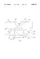
- FIG. 1is a simplified block diagram of a conventional magnetic recording disk drive for use with the MTJ MR read head according to the present invention.
- FIG. 2is a top view of the disk drive of FIG. 1 with the cover removed.
- FIG. 3is a vertical cross-section of a conventional integrated inductive write head/MR read head with the MR read head located between shields and adjacent to the inductive write head.
- FIG. 4is a cross-section of the magnetic tunnel junction layers and conducting leads for use in the MTJ MR read head of the present invention.
- FIGS. 5A and 5Bare top and cross-sectional views of a prior art MTJ read head with electrically isolated longitudinal bias regions to the left and right side of the MTJ device.
- FIG. 6is a top view of the prior art MTJ read head of FIG. 5 illustrating the disposition of the MTJ read head with regard to the air bearing surface.
- FIG. 7illustrates the ferromagnetic coupling field and magnetostatic coupling field acting on an MTJ sensing layer from the pinned or fixed ferromagnetic layer.
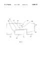
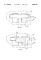
- FIG. 8is a top view of the MTJ MR read head of the present invention with an ferromagnetic bias region around three sides of the tunnel junction which provides both longitudinal and transverse bias fields.
- FIG. 9is a top view of the MTJ MR read head of the present invention with separate ferromagnetic bias regions around three sides of the tunnel junction in which one bias region at the back edge of the tunnel junction provides a transverse bias field while separate regions on the sides of the tunnel junction provide a longitudinal bias field.
- FIGS. 10A-10Eillustrate steps in the fabrication of the MTJ MR read head of the present invention according to FIG. 8.
- FIGS. 11A-11Eillustrate steps in the fabrication of the MTJ MR read head of the present invention according to FIG. 9.
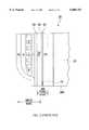
- FIG. 1there is illustrated in sectional view a schematic of a prior art disk drive of the type using a MR sensor.
- the disk drivecomprises a base 10 to which are secured a disk drive motor 12 and an actuator 14, and a cover 11.
- the base 10 and cover 11provide a substantially sealed housing for the disk drive.
- a magnetic recording disk 16is connected to drive motor 12 by means of hub 18 to which it is attached for rotation by the drive motor 12.
- a thin lubricant film 50is maintained on the surface of disk 16.
- a read/write head or transducer 25is formed on the trailing end of a carrier, such as an air-bearing slider 20.
- Transducer 25is a read/write head comprising an inductive write head portion and a MR read head portion, as will be described with respect to FIG. 3.
- the slider 20is connected to the actuator 14 by means of a rigid arm 22 and a suspension 24.
- the suspension 24provides a biasing force which urges the slider 20 onto the surface of the recording disk 16.
- the drive motor 12rotates the disk 16 at a constant speed
- the actuator 14, which is typically a linear or rotary voice coil motor (VCM)moves the slider 20 generally radially across the surface of the disk 16 so that the read/write head 25 may access different data tracks on disk 16.
- VCMlinear or rotary voice coil motor
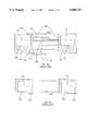
- FIG. 2is a top view of the interior of the disk drive with the cover 11 removed, and illustrates in better detail the suspension 24 which provides a force to the slider 20 to urge it toward the disk 16.
- the suspensionmay be a conventional type of suspension, such as the well-known Watrous suspension, as described in IBM's U.S. Pat. No. 4,167,765. This type of suspension also provides a gimbaled attachment of the slider which allows the slider to pitch and roll as it rides on the air bearing.
- the data detected from disk 16 by the transducer 25is processed into a data readback signal by signal amplification and processing circuitry in the integrated circuit chip 15 located on arm 22.
- the signals from transducer 25travel via flex cable 17 to chip 15, which sends its output signals to the disk drive electronics (not shown) via cable 19.
- FIG. 3is a cross-sectional schematic view of the integrated read/write head 25 which includes a MR read head portion and an inductive write head portion.
- the head 25is lapped to form an air-bearing surface (ABS), the ABS being spaced from the surface of the rotating disk 16 (FIG. 1) by the air bearing as discussed above.
- the read headincludes a MR sensor 40 sandwiched between first and second gap layers G1 and G2 which are, in turn, sandwiched between first and second magnetic shield layers S1 and S2.
- the MR sensor 40is an AMR sensor.
- the write headincludes a coil layer C and insulation layer I2 which are sandwiched between insulation layers I1 and I3 which are, in turn, sandwiched between first and second pole pieces P1 and P2.
- a gap layer G3is sandwiched between the first and second pole pieces P1, P2 at their pole tips adjacent to the ABS for providing a magnetic gap.
- signal currentis conducted through the coil layer C and flux is induced into the first and second pole layers P1, P2 causing flux to fringe across the pole tips at the ABS.
- This fluxmagnetizes circular tracks on the rotating disk 16 during a write operation.
- magnetized regions on the rotating disk 16inject flux into the MR sensor 40 of the read head, causing resistance changes in the MR sensor 40. These resistance changes are detected by detecting voltage changes across the MR sensor 40.
- the voltage changesare processed by the chip 15 (FIG. 2) and drive electronics and converted into user data.
- the combined head 25 shown in FIG. 3is a "merged" head in which the second shield layer S2 of the read head is employed as a first pole piece P1 for the write head. In a piggyback head (not shown), the second shield layer S2 and the first pole piece P1 are separate layers.
- Disk drivesmay contain a large number of disks and actuators, and each actuator may support a number of sliders.
- the head carriermay be one which maintains the head in contact or near contact with the disk, such as in liquid bearing and other contact and near-contact recording disk drives.
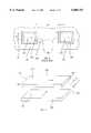
- FIG. 4illustrates a prior art MTJ MR read head with an MTJ sensor for use in place of the MR sensor 40 in the read/write head 25 of FIG. 3.
- a bottom electrical lead 102is formed on a suitable substrate 9.
- the substratemay the gap layer G1 or alternatively the lead 102 may be formed directly on the magnetic shield S1.
- the MTJ 100is then formed as a stack of layers between the bottom electrical lead 102 and a top electrical lead 104.
- the top electrical leadmay be electrically isolated from the shield S2 or may be directly connected to the shield S2 which may form itself part of the electrical circuit to the MTJ device.
- the MTJ 100includes a first or bottom electrode multilayer stack 110, an insulating tunnel barrier layer 120, and a second or top electrode stack 130.
- Each of the electrodesincludes a ferromagnetic layer in direct contact with tunnel barrier layer 120, i.e., ferromagnetic layers 118 and 132.
- the electrode layer stack 110 formed on electrical lead 102includes a seed or "template” layer 112 on the lead 102, a layer of antiferromagnetic material 116 on the template layer 112, and a "fixed” ferromagnetic layer 118 formed on and exchange coupled with the underlying antiferromagnetic layer 116.
- the ferromagnetic layer 118is called the fixed layer because its magnetic moment or magnetization direction is prevented from rotation in the presence of applied magnetic fields in the desired range of interest.
- the top electrode stack 130includes a "free” or “sensing” ferromagnetic layer 132 and a protective or capping layer 134 formed on the sensing layer 132.
- the sensing ferromagnetic layer 132is not exchange coupled to an antiferromagnetic layer, and its magnetization direction is thus free to rotate in the presence of applied magnetic fields in the range of interest.
- the sensing ferromagnetic layer 132is fabricated so as to have its magnetic moment or magnetization direction (shown by arrow 133) oriented generally parallel to the ABS (the ABS is a plane parallel to the paper in FIG. 4; see also FIG. 3) and generally perpendicular to the magnetization direction of the fixed ferromagnetic layer 118 in the absence of an applied magnetic field.
- the fixed ferromagnetic layer 118 in electrode stack 110 just beneath the tunnel barrier layer 120has its magnetization direction fixed by interfacial exchange coupling with the immediately underlying antiferromagnetic layer 116, which also forms part of bottom electrode stack 110.
- the magnetization direction of the fixed ferromagnetic layer 118is oriented generally perpendicular to the ABS, i.e., out of or into the paper in FIG. 4 (as shown by arrow tail 119).
- FIG. 5A and FIG. 5Bshow respectively, a sectional and a top view of the MTJ MR read head of FIG. 4 with additionally a biasing ferrromagnetic layer 150 for longitudinally biasing the magnetization of the sensing ferromagnetic layer 132, and an insulating layer 160 separating and isolating the biasing layer 150 from the sensing ferromagnetic layer 132 and the other layers of the MTJ 100.
- the device of FIGS. 5A-5Bis described in more detail in IBM's U.S. Pat. No. 5,729,410.
- the biasing ferromagnetic layer 150is comprised of a hard magnetic material, such as a CoPtCr alloy, that has its magnetic moment (shown by arrow 151) aligned in the same direction as the magnetic moment 133 of the sensing ferromagnetic layer 132 in the absence of an applied magnetic field.
- the insulating layer 160which is preferably alumina (AI 2 O 3 ) or silica (SiO 2 ), has a thickness sufficient to electrically isolate the biasing ferromagnetic layer 150 from the MTJ 100 and the electrical leads 102, 104, but is still thin enough to permit magnetostatic coupling with the sensing ferromagnetic layer 132.
- the product M*t of the biasing ferromagnetic layer 150(where M is the magnetic moment per unit area of the material in the ferromagnetic layer and t is the thickness of the ferromagnetic layer) must be greater than or equal to the M*t of the sensing ferromagnetic layer 132 to assure stable longitudinal biasing.
- the thickness of the biasing ferromagnetic layer 150is at least approximately twice that of the sensing ferromagnetic layer 132.
- FIG. 6is a similar top view of the MTJ MR head shown in FIG. 5B but showing the disposition of the MTJ head with respect to the ABS.
- the dashed line 161represents the ABS and the line to which the layers are lapped back after the MTJ MR head is fabricated.
- the MTJ 100is depicted as a stripe having a width TW, appropriate to the track width of the recorded data on the disk, and a final stripe height SH after lapping.
- the width of the recorded data trackis typically wider than TW. Note that for purposes of clarity we shall refer to the edges of the MTJ sensor where the longitudinal bias regions 150 are disposed as the left and right edges 180.
- a sense current Iis directed from the first electrical lead 102 perpendicularly through the antiferromagnetic layer 116, the fixed ferromagnetic layer 118, the tunnel barrier layer 120, and the sensing ferromagnetic layer 132 and then out through the second electrical lead 104.
- the amount of tunneling current through the tunnel barrier layer 120is a function of the relative orientations of the magnetizations of the fixed and sensing ferromagnetic layers 118, 132 that are adjacent to and in contact with the tunnel barrier layer 120.
- the magnetic field from the recorded datacauses the magnetization direction of the sensing ferromagnetic layer 132 to rotate away from the direction 133, i.e., either into or out of the paper of FIG. 4.
- This change in resistanceis detected by the disk drive electronics and processed into data read back from the disk.
- the sense currentis prevented from reaching the biasing ferromagnetic layer 150 by the electrical insulating layer 160, which also insulates the biasing ferromagnetic layer 150 from the electrical leads 102, 104.
- FIGS. 5A-5B and 6allow for stabilization of the MTJ ferromagnetic sensing layer into a largely single magnetic domain state.
- the regions 150it is very likely that the magnetic poles which would then be present at the edges 180 of the sensing layer 132 would result in the formation of closure domains at these edges.
- the multi-domain state of the sensing layerwould then give rise to noise and irreproducible signals for otherwise the same sense field.
- the longitudinal bias regionseliminate the closure domains for proper operation of the MTJ read head there is, in addition, a requirement that the response of the head be linear in the applied sense field. This is achieved by properly transversely biasing the magnetic moment of the sensing layer 132.
- the optimum configuration of the MTJ read headis one in which the magnetic moment of the sensing layer 132 is oriented approximately parallel to the ABS 161 and approximately perpendicular to the magnetic moment of the pinned or fixed ferromagnetic layer 118.
- the moment of the fixed ferromagnetic layer 118is oriented largely perpendicular to the ABS.
- the magnetic moment of the sensing layeris arranged such that the MTJ device has maximum sensitivity to the sense field since the tunneling conductance of the MTJ device varies cosinusoidally as the angle between the directions of the magnetic moments of the sensing layer 132 and the fixed layer 118. Moreover, the maximum angular excursion of the magnetic moment of the sensing layer, resulting from the presence of the sense field before saturation of the tunneling conductance of the device, is the same for either direction of the sense field parallel and antiparallel to the normal to the ABS.
- the sensing layer 132has a front edge 182 that faces the ABS, a back edge 190 and side edges 180.
- the orientation of the magnetic moment of the sensing layer 132, in the absence of any sense field,is determined by the net effective magnetic field acting on the sensing ferromagnetic layer. As illustrated schematically in FIG. 7 this is largely the result of a balance between any ferromagnetic coupling field H F between the sensing layer 132 and the fixed ferromagnetic layer 118 and the magnetostatic coupling field H D on the sensing layer arising largely from the magnetic poles at the edges 185 of the fixed ferromagnetic layer.
- the sensing layer 132may exhibit some magnetic anisotropy which may favor the orientation of the magnetic moment of the sensing layer along a particular direction in the plane of the sensing layer.
- the magnetic anisotropymay arise from the intrinsic magnetocrystalline anisotropy of the ferromagnetic material comprising the sensing layer or may be induced via the deposition of the sensing ferromagnetic layer in a magnetic field or via the sensing layer's magnetostriction from stress in the sensing layer, for example, introduced during the processing of the MTJ device.
- the magnetostatic coupling field H Dmay be varied by varying the thickness and magnetic moment of the fixed ferromagnetic layer or by forming the fixed ferromagnetic layer from an antiferromagnetically coupled sandwich of two ferromagnetic layers separated by a thin antiferromagnetically coupling layer, as described in IBM's pending application Ser. No. 08/895,118 filed Jul. 16, 1997.
- the ferromagnetic coupling field H Fmay be varied by introducing a thin non-ferromagnetic layer between the tunnel barrier layer 120 and the ferromagnetic sensing layer 132, as described in IBM's pending application Ser. No. 08/758,614 filed Nov. 27, 1996.
- the use of additional non-ferromagnetic layersreduces the magnitude of the magneto-tunneling response of the MTJ device.
- these methodsrequire a more complicated MTJ device 100 which may be more difficult to manufacture and may require additional deposition sources for the additional layers which may not be available.
- the magnetic moment (and consequently the thickness) of the sensing layermay be fixed by the density of recorded magnetic bits for optimum performance of the magnetic recording read head.
- a mechanism to provide an additional transverse magnetic bias fieldis needed to optimally bias the MTJ device. As illustrated in FIG. 8 such a transverse bias field is provided by a ferromagnetic biasing layer 320 that has longitudinal bias regions 322 near the left and right edges 180 of the sensing layer 132 (as shown in FIG.
- the biasing layer 320will be referred to as the continuous boundary biasing (CBB) layer.
- the front edge 182 of the sensing layer in MTJ sensor 100i.e., the edge located at the ABS, remains uncovered so that magnetic flux from recorded bits in the magnetic medium may be detected by the sensing layer.
- the front edge of the MTJ sensormay be situated directly at the ABS as in FIG. 8 or may be recessed from the ABS and the flux may be brought to the recessed front edge of the sensor by means of a flux guide.
- the use of the additional bias region 324 at the back edge 190allows for a moderate amount of transverse bias field (along the direction indicated by the arrow 382 in FIG.
- a longitudinal bias field(along the direction of the arrow 384 in FIG. 8) may be applied to the MTJ 100 by canting the direction of the magnetic moment of the CBB layer 320 away from the ABS in the plane of the film, as indicated by the arrow 380 in FIG. 8.
- the magnitude of the transverse bias field from the CBB layer 320can be arbitrarily varied, within a certain range, so as to obtain a more complete compensation of the transverse fields H D and H F on the MTJ ferromagnetic sensing layer.
- the CBB layer 320provides a sufficient longitudinal bias field for stabilization of the MTJ sensor.
- the magnetic momentcan have a direction 380 between ⁇ 90 degrees, where 0 degrees corresponds to a purely longitudinal direction parallel to the long edges of the rectangularly shaped sensing layer 132 and in the same direction as the moment of the sensing layer in the absence of an applied field.
- 0 degreescorresponds to a purely longitudinal direction parallel to the long edges of the rectangularly shaped sensing layer 132 and in the same direction as the moment of the sensing layer in the absence of an applied field.
- a CBB layer 425may be formed as three distinct portions, the two longitudinal bias portions 420 at the side edges of the sensing ferromagnetic layer of the MTJ 100 and the rear or back transverse bias portion 425.
- the longitudinal bias fieldis provided by the bias portions 420 at the left and right sides edges 180 of the MTJ 100 but in this embodiment the biasing portion at the rear edge 190 is fabricated as a separate region 425.
- the magnetic moments of the two biasing regions 420 and 425can be independently designed to provide the appropriate strengths and directions of transverse and longitudinal bias fields.
- the direction of the magnetic moments of the transverse and longitudinal bias regions 420 and 425are oriented along a common canting angle along the direction indicated by the arrow 480 in FIG. 9.
- the longitudinal and transverse bias fieldsare along the directions indicated by the arrows 484 and 482 in FIG. 9.
- the canting angle ⁇ T of the transverse bias region 425 and the canting angle ⁇ L of the longitudinal bias region 420may be set at different canting angles.
- a representative set of materials for MTJ 100(FIG. 4) will now be described. All of the layers of the MTJ 100 are grown in the presence of a magnetic field applied parallel to the surface of the substrate. The magnetic field serves to orient the easy axis of all of the ferromagnetic layers.
- a 5 nm Ta seed layer(not shown) is first formed on a 10-50 nm Au layer that serves as the electrical lead 102.
- the seed layeris comprised of a material which encourages the (111) growth of the face-centered cubic (fcc) Ni 81 Fe 19 template layer 112.
- the template ferromagnetic layer 112encourages the growth of the antiferromagnetic layer 116.
- Suitable seed layer materialsinclude fcc metals, such as Cu, as well as Ta or a combination of layers, such as 3-5 nm Ta/3-5 nm Cu.
- the MTJ base electrode stack 110comprises a stack of 4 nm Ni 81 Fe 19 /10 nm Fe 50 Mn 50 /8 nm Ni 81 Fe 19 (layers 112, 116, 118, respectively) grown on the Ta seed layer on the 10-20 nm Au layer 102.
- the Au lead layer 102is formed on the alumina gap material G1 that serves as the substrate.
- the tunnel barrier layer 120is formed by depositing and then plasma oxidizing a 0.5-2 nm AI layer. This creates the AI 2 O 3 insulating tunnel barrier layer 120.
- the top electrode stack 130is a 5 nm Ni--Fe/10 nm Ta stack (layers 132,134, respectively).
- the Ta layer 134serves as a protective capping layer.
- the top electrode stack 130is contacted by a 20 nm Au layer that serves as the electrical lead 104.
- the resistance of the MTJ devicewill be largely dominated by that of the tunnel barrier layer 120.
- the resistance per unit area of the conducting leads 102, 104can be much higher than in conventional MR read heads in which the current flows parallel to the layers.
- the leads 102, 104can be made thinner and/or narrower than in conventional MR head structures, and/or can be made from intrinsically more resistive materials, such as alloys or combinations of elements.
- the layers in the bottom electrode stack 110be smooth, and that the AI 2 O 3 tunnel barrier layer 120 be free of pinholes which would electrically short the junction.
- growth by sputtering techniques known to produce good giant magnetoresistance effects in metallic multilayer stacksis sufficient.
- An alternative sensing ferromagnetic layer 132may be comprised of a thin Co or Co.sub.(100-x) Fe.sub.(x) or Ni.sub.(100-x) Fe x (x is approximately 60) layer at the interface between the sensing ferromagnetic layer 132 and the tunnel barrier layer 120, with the bulk of layer 132 being a low magnetostriction material, such as Ni.sub.(100-x) Fe x (x is approximately 19).
- An alternative fixed ferromagnetic layer 118may be comprised largely of a bulk Ni.sub.(100-x) Fe.sub.(x) layer with a thin layer of a Co or Co.sub.(100-x) Fe.sub.(x) or Ni.sub.(100-x) Fe x (x is approximately 60) layer at the interface with the tunnel barrier layer 120.
- the largest signalis obtained with Co or with the highest polarization Ni.sub.(100-x) Fe x (x is approximately 60) or Co.sub.(100-x) Fe.sub.(x) alloy (x is approximately 70).
- the interface layeris optimally about 1-2 nm thick.
- the net magnetostriction of the combined layeris arranged to be close to zero by small variations of the composition. If the bulk of layer 118 is Ni--Fe, then the composition is Ni 81 Fe 19 , the composition for which bulk Ni--Fe has zero magnetostriction.
- the Fe--Mn antiferromagnetic layer 116may be replaced with a Ni--Mn or Ir--Mn layer or other suitable antiferromagnetic layer which exchange biases the ferromagnetic material in the fixed layer 118 and which has a resistance which is substantially less than that of the AI 2 O 3 barrier layer 120.
- a Ni--Mn or Ir--Mn layer or other suitable antiferromagnetic layerwhich exchange biases the ferromagnetic material in the fixed layer 118 and which has a resistance which is substantially less than that of the AI 2 O 3 barrier layer 120.
- antiferromagnetic oxide layers with sufficient conductivitymay be used.
- the fixed ferromagnetic layerhas its magnetic moment fixed by interfacial exchange coupling with an antiferromagnetic layer
- the fixed ferromagnetic layermay be formed of a magnetically "hard" high coercivity material, thereby avoiding the need for an antiferromagnetic layer.
- the hard fixed ferromagnetic layermay thus be formed from a variety of ferromagnetic materials, such as alloys of Co and one or more other elements, including Co--Pt alloys, Co--Pt--Cr alloys, Co--Cr--Ta alloys, Co--Cr alloys, Co--Sm alloys, Co--Re alloys, Co--Ru alloys, and Co--Ni--X alloys (X ⁇ Pt, Pd, or Cr), as well as a variety of quaternary alloys, such as Co--Ni--Cr--Pt and Co--Pt--Cr--B.
- alloys of Co and one or more other elementsincluding Co--Pt alloys, Co--Pt--Cr alloys, Co--Cr--Ta alloys, Co--Cr alloys, Co--Sm alloys, Co--Re alloys, Co--Ru alloys, and Co--Ni--X alloys
- the MTJ device described and shown in FIG. 4has the fixed ferromagnetic layer on the bottom of MTJ 100
- the devicecan also be formed by depositing the sensing ferromagnetic layer first, followed by the tunnel barrier layer, the fixed ferromagnetic layer, and the antiferromagnetic layer. Such an MTJ device would then have the layers essentially inverted from the MTJ 100 shown in FIG. 4.
- FIGS. 10A-10EThe process for forming the MTJ MR read head with the CBB layer 320 of the present invention will first be described with reference to the process flow diagram of FIGS. 10A-10E. In this series of figures only the top view of the device is shown to illustrate the basic lithographic patterning steps necessary to create the MTJ MR head shown in FIG. 8.
- the substrate (not shown) onto which the layers are depositedis the either the G1 alumina gap layer or the shield S1. Film growths are carried out by magnetron sputtering with argon (Ar) gas with the substrate at ambient temperature. Care must be taken to ensure that the sputter growth produces very smooth films.
- An applied magnetic field of magnitude 20-100 Oe, with the field direction in the plane of the substratemay be used to induce magnetic anisotropy into the ferromagnetic layers as they are grown.
- the aluminum layer which is to become the tunnel barrier layer 120is deposited and then subsequently plasma oxidized at an oxygen pressure of 100 mTorr and a power density of 25 W/cm 2 for 30-240 seconds. This forms the insulating tunnel barrier layer 120 of alumina.
- the plasma oxidation of the aluminum layeris done without breaking vacuum in the process.
- the substratePrior to the deposition of the sensing ferromagnetic layer 132 in the MTJ 100 and after formation of the alumina tunnel barrier layer 120, the substrate is rotated approximately 90 degrees in the plane of the substrate so as to be generally transverse to the applied magnetic field. Alternatively, the external applied magnetic field can be rotated.
- bottom lead 102 and MTJ 100(which includes the top capping layer 134). These layers are then patterned into the shape of the bottom electrical lead 102, a part of which is shown by FIG. 10A.
- FIG. 10Blithography is used to form an open region 325 corresponding to the continuous boundary bias region. This is accomplished by first covering the MTJ 100 with a layer of photoresist 310 which is subsequently exposed and patterned to form the open region 325. This step also defines the effective track width TW of the MTJ 100 as the inside dimension of the opening 325 which is formed. As shown in FIG.
- a positive photoresist 310has been applied to the lead 102 and MTJ 100 and developed to define the track width TW. Subsequently, material in the form of the shape 325 is removed from the MTJ 100 by ion milling down to the electrical lead layer 102.
- capping layer 134By suitable choice of material for capping layer 134 (FIG. 4), it may also be possible to reactively ion etch the capping layer 134 before ion milling the remaining MTJ layers.
- the deposition of the initial alumina insulator layer 330, CoPtCr hard ferromagnetic CBB layer 320, and subsequent alumina insulator layer 330are deposited through the opening 325 in photoresist 310, leaving a region of electrically isolated biasing material that forms the CBB layer 320.
- the insulating layer 330 and the hard ferromagnetic layer 320are formed using three distinct depositions.
- a first alumina depositionforms the bottom portion of layer 330 and also conforms onto the side walls and back wall of the MTJ 100 or the top part or layers of the MTJ 100 (FIG. 4), depending on the depth to which the region 325 is ion milled.
- the thickness of the insulating layer on the side wallis less than on a flat surface. Typical sputter efficiencies on side walls are 1/2 to 3/4 that of the sputter efficiencies on flat surfaces.
- the hard biasing ferromagnetic layer 320is deposited using a directional deposition technique, such as ion beam deposition.
- a directional deposition techniquesuch as ion beam deposition.
- the alumina from the first insulating layer deposition that conforms to the side and back walls of the MTJ 100serves to insulate the CBB layer 320 from the MTJ 100.
- a final insulating layer depositionforms the top region of layer 330 and caps or seals the top surface of the CBB layer 320.
- the initial and subsequent alumina layers 330are preferably formed by RF sputtering to provide full coverage over electrical lead 102 and at the edges of MTJ 100 and are each formed to a thickness of 100-500 ⁇ . This process results in an insulator with high integrity since it is important that the sense current not be shunted through the CBB layer 320.
- the CBB layer 320which is preferably a CoPtCr alloy, is preferably formed by a directional deposition process, such as ion beam sputter deposition, so there is no edge overlap, and is deposited to a thickness of approximately twice the thickness of the sensing layer 132.
- the photoresist 310 and the alumina and hard biasing layers on top of itare then removed in a lift-off process, resulting in an electrically isolated continuous boundary bias region of hard biasing ferromagnetic layer 320 that is located at the left, rear and right side edges of the MTJ 100.
- FIG. 10Cshows the final result of this process and for clarity the insulator isolation edge is shown.
- lithographyis used to form the initial stripe height (before lapping) of the MTJ 100 by deposition and patterning of photoresist 340 (FIG. 10D).
- excess tunnel junction materialis removed by a process of ion milling down to the electrical conductor 102 to complete the definition of the MTJ read head as illustrated in FIG. 10E.
- the fabrication of the MTJ MR head structureis then essentially complete, requiring only the final definition of the electrical leads to the device.
- the first lithography stepdefines both the width of the sensor and the back edge of the sensor.
- this process sequenceprovides only a single continuous boundary bias region 320, which means that the strength of the transverse and longitudinal bias fields cannot be independently varied but are coupled to one another.
- the process sequencecan modified as shown in FIGS. 11A-11E to form the embodiment of the MTJ MR read head shown in FIG. 9.
- FIGS. 11A-EThe process flow sequence required for the MTJ read head of FIG. 9 is illustrated in FIGS. 11A-E.
- This processrequires an additional lithography step to define the separate rear edge transverse bias region 425.
- the processstarts with the sequential deposition of bottom lead 102 and MTJ 100 (which includes the top capping layer 134). These layers are then patterned into the shape of the bottom electrical lead 102, a part of which is shown by FIG. 11A.
- FIG. 11Blithography is used to form the two open regions 421 in which will be deposited the longitudinal bias regions at the left and right edges of the MTJ sensor 100.
- This stepalso defines the effective track width TW of the MTJ 100. As shown in FIG.
- a positive photoresist 410has been applied to the lead 102 and MTJ 100 and developed to define the track width TW. Subsequently, material in the form of the two shapes 421 is removed from the MTJ 100 by ion milling down to the electrical lead layer 102.
- the deposition of the initial alumina insulator layer 430, CoPtCr hard biasing ferromagnetic layer 420, and subsequent alumina insulator layer 430are deposited through the openings 421 in photoresist 410, leaving a region of electrically isolated biasing material that forms the longitudinal biasing ferromagnetic portions 420.
- the initial and subsequent alumina layers 430are preferably formed by RF sputtering to provide full coverage over electrical lead 102 and at the edges of MTJ 100 and are each formed to a thickness of 100-500 ⁇ . This process results in an insulator with high integrity since it is important that the sense current not be shunted through the hard longitudinal biasing regions 420.
- the hard biasing layer 420which is preferably a CoPtCr alloy, is preferably formed directionally by a directional deposition process, such as ion beam sputter deposition, so there is no edge overlap, and is deposited to a thickness of approximately twice the thickness of the sensing layer 132.
- the photoresist 410 and the alumina and hard biasing layers on top of itare then removed in a lift-off process, resulting in electrically isolated longitudinal bias regions 420 that are located at the left and right side edges of the MTJ 100.
- FIG. 11Cshows the final result of this process and for clarity the insulator isolation edge is shown.
- FIG. 11Cshows the final result of this process and for clarity the insulator isolation edge is shown.
- an additional lithography step using photoresist 440is used to define an opening 445 in which will be deposited the ferromagnetic material for the rear transverse bias region 425.
- This lithography stepalso defines the rear edge of the MTJ sensor 100.
- a series of steps of ion milling, deposition of alumina insulator 460 and hard ferromagnetic material and lift-offare performed to form the rear region 425 similar to those described above to form the left and right edge hard bias regions 420, leaving the structure as shown in FIG. 11E.
- lithographyis used to form the initial stripe height (before lapping) of the MTJ 100 by deposition and patterning of photoresist 470 (FIG. 11F).
- the magnetization direction 133 of the ferromagnetic sensing layer 132must be maintained in the direction shown in FIG. 4, i.e., along the longitudinal direction with no transverse components. This is accomplished by balancing the various effective transverse magnetic fields to which the ferromagnetic sensing layer is subjected in the absence of any sense field from the recorded medium. Thus a balance is maintained between predominantly the ferromagnetic coupling field H F between the sensing and fixed ferromagnetic layers, the demagnetization field H D from the fixed ferromagnetic layer and the transverse bias field arising from either the continuous boundary biasing layer 320 or the transverse biasing layer 420.
- H Fdepends critically on the nature of the interfaces between the ferromagnetic films and the actual junction and the thickness of the junction. H F can vary from several Oersteds (Oe) to 20-50 Oe.
- H Ddepends on the geometry of the sensor, i.e., final stripe height SH and fixed ferromagnetic layer thickness t, and the fixed ferromagnetic magnetization M, and varies as [4 ⁇ (t/SH) ⁇ M].
- H d and H Fcan be varied by varying the geometry of the sensor and the characteristics of the interfaces.
- H dcan be minimized by using the laminated antiparallel fixed layer described in the previously-cited IBM U.S. Pat. No. 5,465,185.
- the net magnetic moment of such a layeris equivalent to the difference between the two pinned films, this difference being approximately 5 ⁇ , so that H D is reduced to approximately 4 Oe.
- H Fcan be varied by varying the nature of the interfaces.
- the Fe--Mn layer 116 for exchange coupling with the fixed ferromagnetic layer 118is antiferromagnetic as deposited. However, its magnetization must be realigned so that it can exchange couple the fixed ferromagnetic layer 118 in the proper orientation.
- the structureis placed in an annealing oven and the temperature is raised to approximately 180° C., which is greater than the blocking temperature of Fe--Mn. At this temperature, the Fe--Mn layer no longer gives rise to an exchange anisotropy with the fixed ferromagnetic layer 118.
- An exchange anisotropy of the ferromagnetic layer 118is developed by cooling the pair of layers 116, 118 in a magnetic field.
- the orientation of the magnetization of the fixed ferromagnetic layer 118will be along the direction of the applied magnetic field.
- the applied magnetic field in the annealing oventhus causes the moment of the fixed ferromagnetic layer 118 to be fixed along the required direction perpendicular to the ABS, as shown by the arrow 119 in FIG. 4.
- Thisis a result of cooling the Fe--Mn layer in the presence of the ferromagnetic layer 118, magnetized by the applied magnetic field, in the required direction.
- the magnetization of the fixed ferromagnetic layer 118will not substantially rotate.
- the final stripe height SH of the MTJ 100 in the deviceis formed by lapping the lithographically-formed front sensing edge to a final dimension back to line 161 (FIG. 6), thereby completing the structures shown in FIGS. 8 and 9.
- the biasing ferromagnetic layers 320 and 420, 425may be formed from a single layer of a high coercivity material such as an alloy of Co and one or more other elements, such as a Co--Pt binary alloy, or a Co--Pt--Cr ternary alloy (e.g. Co 75 Pt 12 Cr 13 ) or a Co--Pt--Ni ternary alloy or a Co--Cr--Ta ternary alloy.
- a high coercivity materialsuch as an alloy of Co and one or more other elements, such as a Co--Pt binary alloy, or a Co--Pt--Cr ternary alloy (e.g. Co 75 Pt 12 Cr 13 ) or a Co--Pt--Ni ternary alloy or a Co--Cr--Ta ternary alloy.
- the biasing ferromagnetic layermay be a dual-film structure comprising a first ferromagnetic film and an antiferromagnetic film in contact with and interfacially exchange coupled with the first ferromagnetic film.
- the antiferromagnetic filmsecures the magnetic moment of the first ferromagnetic film in the desired direction.
- the ferromagnetic filmmay be Ni--Fe and the antiferromagnetic film may be Ni--Mn.
- the antiferromagnetic filmmust be made of a material that has a blocking temperature sufficiently distinct from the blocking temperature of the material used for the antiferromagnetic layer 116.
- Ni--Mnhas a blocking temperature of up to higher than approximately 450° C. and Fe--Mn has a blocking temperature of approximately 200° C.
- the exchange bias field provided by the antiferromagnetic layer with the higher blocking temperatureis set first by heating the device to a temperature above this blocking temperature and cooling in a magnetic field oriented along the direction of whichever ferromagnetic layer (either 150 or 118) is exchange coupled to the antiferromagnetic layer with the higher blocking temperature. Then, in a second step, after cooling to a temperature slightly greater than the blocking temperature of the other antiferromagnetic layer, the magnetic field orientation (or alternatively the device orientation) is rotated by 90 degree and the device is further cooled.
- the MTJ devicehas been presented above with respect to its use as a MR read head.
- the inventionis fully applicable to other applications of MR sensors, for example in sensors designed to measure the rotation of a device, e.g., automobile wheels or gears, or to sensors designed to measure linear position.
Landscapes
- Engineering & Computer Science (AREA)
- Chemical & Material Sciences (AREA)
- Nanotechnology (AREA)
- Physics & Mathematics (AREA)
- Crystallography & Structural Chemistry (AREA)
- Manufacturing & Machinery (AREA)
- Condensed Matter Physics & Semiconductors (AREA)
- General Physics & Mathematics (AREA)
- Mathematical Physics (AREA)
- Theoretical Computer Science (AREA)
- Magnetic Heads (AREA)
- Hall/Mr Elements (AREA)
Abstract
Description
Claims (20)
Priority Applications (6)
| Application Number | Priority Date | Filing Date | Title |
|---|---|---|---|
| US09/087,322US6005753A (en) | 1998-05-29 | 1998-05-29 | Magnetic tunnel junction magnetoresistive read head with longitudinal and transverse bias |
| MYPI99001819AMY116029A (en) | 1998-05-29 | 1999-05-07 | Magnetic tunnel junction magnetoresistive read head with longitudinal and transverse bias |
| SG9902429ASG82614A1 (en) | 1998-05-29 | 1999-05-13 | Magnetic tunnel junction magnetoresistive read head with longitudinal and transverse bias |
| CN99106498ACN1113334C (en) | 1998-05-29 | 1999-05-14 | Magnetic tunnel junction magnetoresistive read head with longitudinal and transverse bias |
| KR1019990018344AKR100304024B1 (en) | 1998-05-29 | 1999-05-20 | Magnetic tunnel junction magnetoresistive read head with longitudinal and transverse bias |
| JP14418599AJP3177229B2 (en) | 1998-05-29 | 1999-05-25 | Magnetic tunnel junction type magnetoresistive read head with longitudinal and lateral bias |
Applications Claiming Priority (1)
| Application Number | Priority Date | Filing Date | Title |
|---|---|---|---|
| US09/087,322US6005753A (en) | 1998-05-29 | 1998-05-29 | Magnetic tunnel junction magnetoresistive read head with longitudinal and transverse bias |
Publications (1)
| Publication Number | Publication Date |
|---|---|
| US6005753Atrue US6005753A (en) | 1999-12-21 |
Family
ID=22204484
Family Applications (1)
| Application Number | Title | Priority Date | Filing Date |
|---|---|---|---|
| US09/087,322Expired - LifetimeUS6005753A (en) | 1998-05-29 | 1998-05-29 | Magnetic tunnel junction magnetoresistive read head with longitudinal and transverse bias |
Country Status (6)
| Country | Link |
|---|---|
| US (1) | US6005753A (en) |
| JP (1) | JP3177229B2 (en) |
| KR (1) | KR100304024B1 (en) |
| CN (1) | CN1113334C (en) |
| MY (1) | MY116029A (en) |
| SG (1) | SG82614A1 (en) |
Cited By (70)
| Publication number | Priority date | Publication date | Assignee | Title |
|---|---|---|---|---|
| US6178074B1 (en)* | 1998-11-19 | 2001-01-23 | International Business Machines Corporation | Double tunnel junction with magnetoresistance enhancement layer |
| US6183859B1 (en)* | 1998-07-20 | 2001-02-06 | Motorola, Inc | Low resistance MTJ |
| US6333842B1 (en)* | 1997-12-05 | 2001-12-25 | Nec Corporation | Magneto-resistance effect type composite head and production method thereof |
| US6344954B1 (en)* | 1999-07-02 | 2002-02-05 | Tdk Corporation | Magneto-resistive tunnel junction head with specific flux guide structure |
| US6421212B1 (en)* | 1999-09-21 | 2002-07-16 | Read-Rite Corporation | Thin film read head structure with improved bias magnet-to-magnetoresistive element interface and method of fabrication |
| US6462919B1 (en)* | 1999-04-28 | 2002-10-08 | Seagate Technology Llc | Spin valve sensor with exchange tabs |
| WO2002088765A1 (en)* | 2001-04-24 | 2002-11-07 | Matsushita Electric Industrial Co., Ltd. | Magnetoresistive element and magnetoresistive magnetic head, magnetic recording apparatus and magnetoresistive memory device using the same |
| US6480411B1 (en)* | 1999-10-25 | 2002-11-12 | Canon Kabushiki Kaisha | Magnetoresistance effect type memory, and method and device for reproducing information from the memory |
| WO2003001225A1 (en)* | 2001-06-06 | 2003-01-03 | Brown University Research Foundation | Scanning magnetic microscope having improved magnetic sensor |
| US20030011946A1 (en)* | 2001-07-10 | 2003-01-16 | International Business Machines Corporation | Method and apparatus for achieving physical connection between the flux guide and the free layer and that insulates the flux guide from the shields |
| US6512660B1 (en)* | 2000-08-07 | 2003-01-28 | Tdk Corporation | Current perpendicular-to-the-plane magnetoresistance read head with longitudinal or transverse bias provided by current |
| US20030030948A1 (en)* | 2001-08-13 | 2003-02-13 | Eiji Umetsu | CPP type magnetic sensor or magnetic sensor using tunnel effect, and manufacturing method therefor |
| US6542340B1 (en)* | 1999-09-01 | 2003-04-01 | Nec Corporation | Magnetoresistance element, manufacturing method thereof, magnetic field detection system and magnetic recording system |
| US20030086216A1 (en)* | 2001-10-25 | 2003-05-08 | Tdk Corporation | Magneto-resistive device, and magnetic head and head suspension assembly using same |
| US6563679B1 (en) | 2000-08-08 | 2003-05-13 | Tdk Corporation | Current perpendicular-to-the-plane magnetoresistance read heads with transverse magnetic bias |
| US20030134096A1 (en)* | 2000-04-28 | 2003-07-17 | Chen Eugene Youjun | Magnetic element with insulating veils and fabricating method thereof |
| US6597546B2 (en)* | 2001-04-19 | 2003-07-22 | International Business Machines Corporation | Tunnel junction sensor with an antiferromagnetic (AFM) coupled flux guide |
| US20030137780A1 (en)* | 2002-01-18 | 2003-07-24 | International Business Machines Corporation | High linear density tunnel junction flux guide read head with in-stack longitudinal bias stack (LBS) |
| US20030178705A1 (en)* | 2002-03-25 | 2003-09-25 | International Business Machines | System and method for stabilizing a magnetic tunnel junction sensor |
| US6657825B2 (en) | 2001-08-02 | 2003-12-02 | International Business Machines Corporation | Self aligned magnetoresistive flux guide read head with exchange bias underneath free layer |
| US6661625B1 (en) | 2001-02-20 | 2003-12-09 | Kyusik Sin | Spin-dependent tunneling sensor with low resistance metal oxide tunnel barrier |
| US6667862B2 (en) | 2001-02-20 | 2003-12-23 | Carnegie Mellon University | Magnetoresistive read head having permanent magnet on top of magnetoresistive element |
| US6671141B2 (en)* | 2000-03-17 | 2003-12-30 | Tdk Corporation | Tunnel magnetoresistive effective element, a thin film magnetic head, a magnetic head device and a magnetic disk drive device |
| US20040038596A1 (en)* | 2000-04-15 | 2004-02-26 | Mario Bartholoma | Plug-in connector with a bushing |
| US6700759B1 (en) | 2000-06-02 | 2004-03-02 | Western Digital (Fremont), Inc. | Narrow track width magnetoresistive sensor and method of making |
| US6704175B2 (en) | 2001-03-28 | 2004-03-09 | Tdk Corporation | Current perpendicular-to-the-plane magnetoresistance read head |
| US20040047083A1 (en)* | 2000-07-17 | 2004-03-11 | Naoya Hasegawa | Tunneling magneoresistive element and method of manufacturing the same |
| US6724586B2 (en) | 2001-03-27 | 2004-04-20 | Hitachi Global Storage Technologies Netherlands B.V. | Bias structure for magnetic tunnel junction magnetoresistive sensor |
| US20040095690A1 (en)* | 2001-03-14 | 2004-05-20 | Beach Robert S. | Method of simultaneously initializing two antiferromagnetic layers in a magnetic sensor |
| US20040115839A1 (en)* | 2002-04-23 | 2004-06-17 | Matsushita Electric Industrial Co., | Magnetoresistive element and method for producing the same, as well as magnetic head, magnetic memory and magnetic recording device using the same |
| US6754056B2 (en) | 2002-01-18 | 2004-06-22 | International Business Machines Corporation | Read head having a tunnel junction sensor with a free layer biased by exchange coupling with insulating antiferromagnetic (AFM) layers |
| US6757144B2 (en) | 2002-01-18 | 2004-06-29 | International Business Machines Corporation | Flux guide read head with in stack biased current perpendicular to the planes (CPP) sensor |
| US20040196681A1 (en)* | 2002-03-25 | 2004-10-07 | Gang Xiao | Reduction of noise, and optimization of magnetic field sensitivity and electrical properties in magnetic tunnel junction devices |
| US6833982B2 (en) | 2001-05-03 | 2004-12-21 | Hitachi Global Storage Technologies Netherlands B.V. | Magnetic tunnel junction sensor with a free layer biased by longitudinal layers interfacing top surfaces of free layer extensions which extend beyond an active region of the sensor |
| US20050018365A1 (en)* | 2003-07-25 | 2005-01-27 | Hitachi Global Storage Technologies | Structure providing enhanced self-pinning for CPP GMR and tunnel valve heads |
| US20050063100A1 (en)* | 2003-09-23 | 2005-03-24 | Seagate Technology Llc | Magnetic sensor with adjustable electrical dimensions |
| US20050088789A1 (en)* | 2003-10-27 | 2005-04-28 | Seagate Technology Llc | Biasing for tri-layer magnetoresistive sensors |
| US6950290B2 (en)* | 1998-11-30 | 2005-09-27 | Nec Corporation | Magnetoresistive effect transducer having longitudinal bias layer directly connected to free layer |
| US6956763B2 (en) | 2003-06-27 | 2005-10-18 | Freescale Semiconductor, Inc. | MRAM element and methods for writing the MRAM element |
| US6967366B2 (en) | 2003-08-25 | 2005-11-22 | Freescale Semiconductor, Inc. | Magnetoresistive random access memory with reduced switching field variation |
| US20060002032A1 (en)* | 2004-06-30 | 2006-01-05 | Seagate Technology Llc | Differential/dual CPP recording head |
| US20060092582A1 (en)* | 2004-11-04 | 2006-05-04 | Hitachi Global Storage Technologies | CPP sensor having hard bias stabilization placed at back edge of the stripe |
| US20060232893A1 (en)* | 2005-04-18 | 2006-10-19 | Hitachi Global Storage Technologies | Current in plane magnetoresistive sensor having a contiguous hard bias layer located at back edge of stripe height |
| US7129098B2 (en) | 2004-11-24 | 2006-10-31 | Freescale Semiconductor, Inc. | Reduced power magnetoresistive random access memory elements |
| US7145330B2 (en) | 2002-08-16 | 2006-12-05 | Brown University Research Foundation | Scanning magnetic microscope having improved magnetic sensor |
| US7151654B1 (en)* | 2002-03-12 | 2006-12-19 | Seagate Technology Llc | TMR head structure with conductive shunt |
| US20060291107A1 (en)* | 2005-06-22 | 2006-12-28 | Tdk Corporation | Magnetoresistive element with tilted in-stack bias |
| US7184300B2 (en) | 2001-10-16 | 2007-02-27 | Freescale Semiconductor, Inc. | Magneto resistance random access memory element |
| US20070076331A1 (en)* | 2005-10-05 | 2007-04-05 | Hitachi Global Storage Technologies | Magnetoresistive sensor having an improved pinning structure |
| US7224556B2 (en) | 2002-10-24 | 2007-05-29 | Hitachi Global Storage Technologies Netherlands B.V. | Self-pinned CPP magnetoresistive sensor |
| US20070217085A1 (en)* | 2006-03-14 | 2007-09-20 | Hitachi Global Storage Technologies | Current perpendicular to plane (CPP) magnetoresistive sensor with free layer biasing by exchange pinning at back edge |
| US7423826B2 (en) | 2006-03-10 | 2008-09-09 | Seagate Technology Llc | Readback system providing a combined sample output including multiple samples per bit |
| US20080285178A1 (en)* | 2007-05-16 | 2008-11-20 | Tdk Corporation | Thin film magnetic head characterized in bias-applying layer |
| US7465589B2 (en) | 2002-07-17 | 2008-12-16 | Everspin Technologies, Inc. | Multi-state magnetoresistance random access cell with improved memory storage density |
| US20090021870A1 (en)* | 2007-07-17 | 2009-01-22 | Mustafa Michael Pinarbasi | Magnetic head having CPP sensor with improved stabilization of the magnetization of the pinned magnetic layer |
| US20090034126A1 (en)* | 2007-08-01 | 2009-02-05 | Mustafa Michael Pinarbasi | Magnetic head having CPP sensor with improved biasing for free magnetic layer |
| US20090080125A1 (en)* | 2007-03-20 | 2009-03-26 | Fujitsu Limited | Magnetic head |
| US20090166331A1 (en)* | 2007-12-28 | 2009-07-02 | Arley Cleveland Marley | Dynamic hard magnet thickness adjustment for reduced variation in free layer stabilization field in a magnetoresistive sensor |
| US20100328823A1 (en)* | 2009-06-25 | 2010-12-30 | Seagate Technology Llc | Magnetoresistive reader with demagnetization flux guide |
| US20110215800A1 (en)* | 2010-03-05 | 2011-09-08 | Headway Technologies, Inc. | MR sensor with flux guide enhanced hard bias structure |
| US20120218667A1 (en)* | 2009-09-29 | 2012-08-30 | Kabushiki Kaisha Toshiba | Magnetic oscillator |
| US8514525B2 (en) | 2010-09-13 | 2013-08-20 | HGST Netherlands B.V. | Current-perpendicular-to-the-plane (CPP) magnetoresistive (MR) sensor with reference layer integrated in magnetic shield |
| US8701274B2 (en) | 2011-12-30 | 2014-04-22 | HGST Netherlands B.V. | Method for manufacturing a magnetic head |
| US8797694B2 (en) | 2011-12-22 | 2014-08-05 | HGST Netherlands B.V. | Magnetic sensor having hard bias structure for optimized hard bias field and hard bias coercivity |
| US8873203B2 (en)* | 2012-12-21 | 2014-10-28 | HGST Netherlands B.V. | Magnetic head having a soft magnetic layer formed behind a tunneling magnetoresistance (TMR) sensor in an element height direction |
| US8907666B2 (en) | 2011-09-30 | 2014-12-09 | HGST Netherlands B.V. | Magnetic bias structure for magnetoresistive sensor having a scissor structure |
| DE102019107444A1 (en) | 2018-03-23 | 2019-09-26 | Tdk Corporation | Magnetoresistive device |
| US11276423B1 (en)* | 2020-07-02 | 2022-03-15 | Seagate Technology Llc | Reader with a compensating layer |
| US11380355B2 (en)* | 2020-10-27 | 2022-07-05 | Headway Technologies, Inc. | Adaptive bias control for magnetic recording head |
| US20230122220A1 (en)* | 2021-10-14 | 2023-04-20 | Seagate Technology Llc | Shielding structure for a magnetic storage reader |
Families Citing this family (6)
| Publication number | Priority date | Publication date | Assignee | Title |
|---|---|---|---|---|
| US6738234B1 (en)* | 2000-03-15 | 2004-05-18 | Tdk Corporation | Thin film magnetic head and magnetic transducer |
| JP3474523B2 (en)* | 2000-06-30 | 2003-12-08 | Tdk株式会社 | Thin film magnetic head and method of manufacturing the same |
| JP4693292B2 (en)* | 2000-09-11 | 2011-06-01 | 株式会社東芝 | Ferromagnetic tunnel junction device and manufacturing method thereof |
| KR100754304B1 (en)* | 2002-12-20 | 2007-09-03 | 인터내셔널 비지네스 머신즈 코포레이션 | Method for measuring magnetostriction in magnetoresistive elements |
| KR100688577B1 (en)* | 2005-10-14 | 2007-03-02 | 삼성전자주식회사 | Magnetic Heads, Disk Drive Systems Employing the Same, and Method for Correcting Asymmetry of Magnetic Heads |
| KR102678768B1 (en)* | 2015-10-29 | 2024-06-27 | 삼성전자주식회사 | Method of forming layers and method of forming magnetic memory devices using the same |
Citations (18)
| Publication number | Priority date | Publication date | Assignee | Title |
|---|---|---|---|---|
| US3623038A (en)* | 1969-12-19 | 1971-11-23 | Gte Sylvania Inc | Pheral layer magnetic thin film element |
| US4277808A (en)* | 1978-05-26 | 1981-07-07 | Sony Corporation | Magnetic transducer head |
| US4899240A (en)* | 1988-07-28 | 1990-02-06 | Eastman Kodak Company | Biasing for a UMR head |
| US4972284A (en)* | 1989-01-03 | 1990-11-20 | Eastman Kodak Company | Deposited permanent magnet for hard and easy axes biasing of a magnetoresistive head |
| US4987508A (en)* | 1988-12-23 | 1991-01-22 | Eastman Kodak Company | Permanent magnet shaped to provide uniform biasing of a magnetoresistive reproduce head |
| US5018037A (en)* | 1989-10-10 | 1991-05-21 | Krounbi Mohamad T | Magnetoresistive read transducer having hard magnetic bias |
| US5021909A (en)* | 1988-04-20 | 1991-06-04 | Sharp Kabushiki Kaisha | Yoke type thin-film magnetic head and method for suppressing Barkhausen noise |
| US5390061A (en)* | 1990-06-08 | 1995-02-14 | Hitachi, Ltd. | Multilayer magnetoresistance effect-type magnetic head |
| WO1995010123A1 (en)* | 1993-10-06 | 1995-04-13 | Philips Electronics N.V. | Magneto-resistance device, and magnetic head employing such a device |
| US5416353A (en)* | 1992-09-11 | 1995-05-16 | Kabushiki Kaisha Toshiba | Netoresistance effect element |
| US5428491A (en)* | 1993-12-03 | 1995-06-27 | Eastman Kodak Company | Magnetoresistive head with deposited biasing magnet |
| US5432734A (en)* | 1993-08-30 | 1995-07-11 | Mitsubishi Denki Kabushiki Kaisha | Magnetoresistive element and devices utilizing the same |
| US5465185A (en)* | 1993-10-15 | 1995-11-07 | International Business Machines Corporation | Magnetoresistive spin valve sensor with improved pinned ferromagnetic layer and magnetic recording system using the sensor |
| US5528440A (en)* | 1994-07-26 | 1996-06-18 | International Business Machines Corporation | Spin valve magnetoresistive element with longitudinal exchange biasing of end regions abutting the free layer, and magnetic recording system using the element |
| US5650958A (en)* | 1996-03-18 | 1997-07-22 | International Business Machines Corporation | Magnetic tunnel junctions with controlled magnetic response |
| US5729410A (en)* | 1996-11-27 | 1998-03-17 | International Business Machines Corporation | Magnetic tunnel junction device with longitudinal biasing |
| US5764567A (en)* | 1996-11-27 | 1998-06-09 | International Business Machines Corporation | Magnetic tunnel junction device with nonferromagnetic interface layer for improved magnetic field response |
| US5801984A (en)* | 1996-11-27 | 1998-09-01 | International Business Machines Corporation | Magnetic tunnel junction device with ferromagnetic multilayer having fixed magnetic moment |
- 1998
- 1998-05-29USUS09/087,322patent/US6005753A/ennot_activeExpired - Lifetime
- 1999
- 1999-05-07MYMYPI99001819Apatent/MY116029A/enunknown
- 1999-05-13SGSG9902429Apatent/SG82614A1/enunknown
- 1999-05-14CNCN99106498Apatent/CN1113334C/ennot_activeExpired - Fee Related
- 1999-05-20KRKR1019990018344Apatent/KR100304024B1/ennot_activeExpired - Fee Related
- 1999-05-25JPJP14418599Apatent/JP3177229B2/ennot_activeExpired - Fee Related
Patent Citations (18)
| Publication number | Priority date | Publication date | Assignee | Title |
|---|---|---|---|---|
| US3623038A (en)* | 1969-12-19 | 1971-11-23 | Gte Sylvania Inc | Pheral layer magnetic thin film element |
| US4277808A (en)* | 1978-05-26 | 1981-07-07 | Sony Corporation | Magnetic transducer head |
| US5021909A (en)* | 1988-04-20 | 1991-06-04 | Sharp Kabushiki Kaisha | Yoke type thin-film magnetic head and method for suppressing Barkhausen noise |
| US4899240A (en)* | 1988-07-28 | 1990-02-06 | Eastman Kodak Company | Biasing for a UMR head |
| US4987508A (en)* | 1988-12-23 | 1991-01-22 | Eastman Kodak Company | Permanent magnet shaped to provide uniform biasing of a magnetoresistive reproduce head |
| US4972284A (en)* | 1989-01-03 | 1990-11-20 | Eastman Kodak Company | Deposited permanent magnet for hard and easy axes biasing of a magnetoresistive head |
| US5018037A (en)* | 1989-10-10 | 1991-05-21 | Krounbi Mohamad T | Magnetoresistive read transducer having hard magnetic bias |
| US5390061A (en)* | 1990-06-08 | 1995-02-14 | Hitachi, Ltd. | Multilayer magnetoresistance effect-type magnetic head |
| US5416353A (en)* | 1992-09-11 | 1995-05-16 | Kabushiki Kaisha Toshiba | Netoresistance effect element |
| US5432734A (en)* | 1993-08-30 | 1995-07-11 | Mitsubishi Denki Kabushiki Kaisha | Magnetoresistive element and devices utilizing the same |
| WO1995010123A1 (en)* | 1993-10-06 | 1995-04-13 | Philips Electronics N.V. | Magneto-resistance device, and magnetic head employing such a device |
| US5465185A (en)* | 1993-10-15 | 1995-11-07 | International Business Machines Corporation | Magnetoresistive spin valve sensor with improved pinned ferromagnetic layer and magnetic recording system using the sensor |
| US5428491A (en)* | 1993-12-03 | 1995-06-27 | Eastman Kodak Company | Magnetoresistive head with deposited biasing magnet |
| US5528440A (en)* | 1994-07-26 | 1996-06-18 | International Business Machines Corporation | Spin valve magnetoresistive element with longitudinal exchange biasing of end regions abutting the free layer, and magnetic recording system using the element |
| US5650958A (en)* | 1996-03-18 | 1997-07-22 | International Business Machines Corporation | Magnetic tunnel junctions with controlled magnetic response |
| US5729410A (en)* | 1996-11-27 | 1998-03-17 | International Business Machines Corporation | Magnetic tunnel junction device with longitudinal biasing |
| US5764567A (en)* | 1996-11-27 | 1998-06-09 | International Business Machines Corporation | Magnetic tunnel junction device with nonferromagnetic interface layer for improved magnetic field response |
| US5801984A (en)* | 1996-11-27 | 1998-09-01 | International Business Machines Corporation | Magnetic tunnel junction device with ferromagnetic multilayer having fixed magnetic moment |
Non-Patent Citations (6)
| Title |
|---|
| J. S. Moodera et al., "Ferromagnetic-insulator-ferromagnetic Tunneling: Spin-dependent Tunneling and Large Magnetoresistance in Trilayer Junctions", Symposium on Spin Tunneling and Injection Phenomena, Journal of Applied Physics, vol. 79, No. 8, Apr. 15, 1996, pp. 4724-4729. |
| J. S. Moodera et al., Ferromagnetic insulator ferromagnetic Tunneling: Spin dependent Tunneling and Large Magnetoresistance in Trilayer Junctions , Symposium on Spin Tunneling and Injection Phenomena, Journal of Applied Physics, vol. 79, No. 8, Apr. 15, 1996, pp. 4724 4729.* |
| K. Matsuyama et al., "Fabrication of Microstructured Magnetic Tunneling Valve Junction", IEEE Transactions on Magnetics, vol. 31, NO. 6, Nov. 1995, pp. 3176-3178. |
| K. Matsuyama et al., Fabrication of Microstructured Magnetic Tunneling Valve Junction , IEEE Transactions on Magnetics, vol. 31, NO. 6, Nov. 1995, pp. 3176 3178.* |
| M. Julliere, "Tunneling Between Ferromagnetic Films", Physics Letters, vol. 54A, No. 3, Sep. 8, 1975, pp. 225-226. |
| M. Julliere, Tunneling Between Ferromagnetic Films , Physics Letters, vol. 54A, No. 3, Sep. 8, 1975, pp. 225 226.* |
Cited By (119)
| Publication number | Priority date | Publication date | Assignee | Title |
|---|---|---|---|---|
| US6333842B1 (en)* | 1997-12-05 | 2001-12-25 | Nec Corporation | Magneto-resistance effect type composite head and production method thereof |
| US6639766B2 (en) | 1997-12-05 | 2003-10-28 | Nec Corporation | Magneto-resistance effect type composite head and production method thereof |
| US6183859B1 (en)* | 1998-07-20 | 2001-02-06 | Motorola, Inc | Low resistance MTJ |
| US6261646B1 (en) | 1998-07-20 | 2001-07-17 | Motorola, Inc. | Method of making a low resistance MTJ |
| US6178074B1 (en)* | 1998-11-19 | 2001-01-23 | International Business Machines Corporation | Double tunnel junction with magnetoresistance enhancement layer |
| US6606781B1 (en)* | 1998-11-19 | 2003-08-19 | Hitachi Global Storage Technologies Netherlands B.V. | Method of making double tunnel junction with magnetoresistance enhancement layer |
| US6950290B2 (en)* | 1998-11-30 | 2005-09-27 | Nec Corporation | Magnetoresistive effect transducer having longitudinal bias layer directly connected to free layer |
| US6462919B1 (en)* | 1999-04-28 | 2002-10-08 | Seagate Technology Llc | Spin valve sensor with exchange tabs |
| US6344954B1 (en)* | 1999-07-02 | 2002-02-05 | Tdk Corporation | Magneto-resistive tunnel junction head with specific flux guide structure |
| US6542340B1 (en)* | 1999-09-01 | 2003-04-01 | Nec Corporation | Magnetoresistance element, manufacturing method thereof, magnetic field detection system and magnetic recording system |
| US6735850B1 (en) | 1999-09-21 | 2004-05-18 | Western Digital (Fremont), Inc. | Thin film read head structure with improved bias magnet-to-magnetoresistive element interface and method of fabrication |
| US6421212B1 (en)* | 1999-09-21 | 2002-07-16 | Read-Rite Corporation | Thin film read head structure with improved bias magnet-to-magnetoresistive element interface and method of fabrication |
| US6480411B1 (en)* | 1999-10-25 | 2002-11-12 | Canon Kabushiki Kaisha | Magnetoresistance effect type memory, and method and device for reproducing information from the memory |
| US6671141B2 (en)* | 2000-03-17 | 2003-12-30 | Tdk Corporation | Tunnel magnetoresistive effective element, a thin film magnetic head, a magnetic head device and a magnetic disk drive device |
| US20040038596A1 (en)* | 2000-04-15 | 2004-02-26 | Mario Bartholoma | Plug-in connector with a bushing |
| US6835423B2 (en) | 2000-04-28 | 2004-12-28 | Freescale Semiconductor, Inc. | Method of fabricating a magnetic element with insulating veils |
| US20030134096A1 (en)* | 2000-04-28 | 2003-07-17 | Chen Eugene Youjun | Magnetic element with insulating veils and fabricating method thereof |
| US7134185B1 (en) | 2000-06-02 | 2006-11-14 | Western Digital (Fremont), Inc. | Method of making narrow track width magnetoresistive sensor |
| US6700759B1 (en) | 2000-06-02 | 2004-03-02 | Western Digital (Fremont), Inc. | Narrow track width magnetoresistive sensor and method of making |
| US6657431B2 (en)* | 2000-06-06 | 2003-12-02 | Brown University Research Foundation | Scanning magnetic microscope having improved magnetic sensor |
| US6751073B2 (en) | 2000-07-17 | 2004-06-15 | Alps Electric Co., Ltd. | Tunneling magnetoresistive element and method of manufacturing the same |
| US7178222B2 (en) | 2000-07-17 | 2007-02-20 | Alps Electric Co., Ltd. | Method of manufacturing a tunneling magnetoresistive element |
| US20040047083A1 (en)* | 2000-07-17 | 2004-03-11 | Naoya Hasegawa | Tunneling magneoresistive element and method of manufacturing the same |
| US6512660B1 (en)* | 2000-08-07 | 2003-01-28 | Tdk Corporation | Current perpendicular-to-the-plane magnetoresistance read head with longitudinal or transverse bias provided by current |
| US6563679B1 (en) | 2000-08-08 | 2003-05-13 | Tdk Corporation | Current perpendicular-to-the-plane magnetoresistance read heads with transverse magnetic bias |
| US6661625B1 (en) | 2001-02-20 | 2003-12-09 | Kyusik Sin | Spin-dependent tunneling sensor with low resistance metal oxide tunnel barrier |
| US6667862B2 (en) | 2001-02-20 | 2003-12-23 | Carnegie Mellon University | Magnetoresistive read head having permanent magnet on top of magnetoresistive element |
| US7166173B2 (en) | 2001-03-14 | 2007-01-23 | Hitachi Global Storage Technologies Netherlands B.V. | Method of simultaneously initializing two antiferromagnetic layers in a magnetic sensor |
| US20040095690A1 (en)* | 2001-03-14 | 2004-05-20 | Beach Robert S. | Method of simultaneously initializing two antiferromagnetic layers in a magnetic sensor |
| US6724586B2 (en) | 2001-03-27 | 2004-04-20 | Hitachi Global Storage Technologies Netherlands B.V. | Bias structure for magnetic tunnel junction magnetoresistive sensor |
| US6704175B2 (en) | 2001-03-28 | 2004-03-09 | Tdk Corporation | Current perpendicular-to-the-plane magnetoresistance read head |
| US6597546B2 (en)* | 2001-04-19 | 2003-07-22 | International Business Machines Corporation | Tunnel junction sensor with an antiferromagnetic (AFM) coupled flux guide |
| US7079361B2 (en) | 2001-04-24 | 2006-07-18 | Matsushita Electric Industrial Co., Ltd. | Magnetoresistive element and magnetoresistive magnetic head, magnetic recording apparatus and magnetoresistive memory device using the same |
| US20050135020A1 (en)* | 2001-04-24 | 2005-06-23 | Matsushita Electric Industrial Co., Ltd. | Magnetoresistive element and magetoresistive magnetic head, magnetic recording apparatus and magnetoresistive memory device using the same |
| WO2002088765A1 (en)* | 2001-04-24 | 2002-11-07 | Matsushita Electric Industrial Co., Ltd. | Magnetoresistive element and magnetoresistive magnetic head, magnetic recording apparatus and magnetoresistive memory device using the same |
| US6833982B2 (en) | 2001-05-03 | 2004-12-21 | Hitachi Global Storage Technologies Netherlands B.V. | Magnetic tunnel junction sensor with a free layer biased by longitudinal layers interfacing top surfaces of free layer extensions which extend beyond an active region of the sensor |
| WO2003001225A1 (en)* | 2001-06-06 | 2003-01-03 | Brown University Research Foundation | Scanning magnetic microscope having improved magnetic sensor |
| US20030011946A1 (en)* | 2001-07-10 | 2003-01-16 | International Business Machines Corporation | Method and apparatus for achieving physical connection between the flux guide and the free layer and that insulates the flux guide from the shields |
| US7057864B2 (en) | 2001-07-10 | 2006-06-06 | Hitachi Global Storage Technologies Netherlands B.V. | Method and apparatus for achieving physical connection between the flux guide and the free layer and that insulates the flux guide from the shields |
| US20050064092A1 (en)* | 2001-07-10 | 2005-03-24 | Hitachi Global Storage Technologies Netherlands B.V. | Method and apparatus for achieving physical connection between the flux guide and the free layer and that insulates the flux guide from the shields |
| US7237322B2 (en) | 2001-07-10 | 2007-07-03 | Hitachi Global Storage Technologies Netherlands B.V. | Method for making a tunnel valve head with a flux guide |
| US7036208B2 (en) | 2001-08-02 | 2006-05-02 | Hitachi Global Storagetechnologies Netherlands B.V | Self aligned magnetoresistive flux guide read head with exchange bias underneath free layer |
| US20040061979A1 (en)* | 2001-08-02 | 2004-04-01 | Ho Kuok San | Self aligned magnetoresistive flux guide read head with exchange bias underneath free layer |
| US6657825B2 (en) | 2001-08-02 | 2003-12-02 | International Business Machines Corporation | Self aligned magnetoresistive flux guide read head with exchange bias underneath free layer |
| US6826022B2 (en) | 2001-08-13 | 2004-11-30 | Alps Electric Co., Ltd. | CPP type magnetic sensor or magnetic sensor using tunnel effect, and manufacturing method therefor |
| US20030030948A1 (en)* | 2001-08-13 | 2003-02-13 | Eiji Umetsu | CPP type magnetic sensor or magnetic sensor using tunnel effect, and manufacturing method therefor |
| US7184300B2 (en) | 2001-10-16 | 2007-02-27 | Freescale Semiconductor, Inc. | Magneto resistance random access memory element |
| US6992870B2 (en) | 2001-10-25 | 2006-01-31 | Tdk Corporation | Magneto-resistive device, and magnetic head and head suspension assembly using same |
| US20030086216A1 (en)* | 2001-10-25 | 2003-05-08 | Tdk Corporation | Magneto-resistive device, and magnetic head and head suspension assembly using same |
| US7161773B2 (en) | 2002-01-18 | 2007-01-09 | Hitachi Global Storage Technologies Netherlands B.V. | High linear density tunnel junction flux guide read head with in-stack longitudinal bias stack (LBS) |
| US20030137780A1 (en)* | 2002-01-18 | 2003-07-24 | International Business Machines Corporation | High linear density tunnel junction flux guide read head with in-stack longitudinal bias stack (LBS) |
| US20050146812A1 (en)* | 2002-01-18 | 2005-07-07 | Hitachi Global Storage Technologies Netherlands B.V. | High linear density tunnel junction flux guide read head with in-stack longitudinal bias stack (LBS) |
| US6757144B2 (en) | 2002-01-18 | 2004-06-29 | International Business Machines Corporation | Flux guide read head with in stack biased current perpendicular to the planes (CPP) sensor |
| US6754056B2 (en) | 2002-01-18 | 2004-06-22 | International Business Machines Corporation | Read head having a tunnel junction sensor with a free layer biased by exchange coupling with insulating antiferromagnetic (AFM) layers |
| US6888705B2 (en) | 2002-01-18 | 2005-05-03 | Hitachi Global Storage Technologies Netherlands B.V. | High linear density tunnel junction flux guide read head with in-stack longitudinal bias stack (LBS) |
| US20040196596A1 (en)* | 2002-01-18 | 2004-10-07 | Ho Kuok San | Method of making a read head having a tunnel junction sensor with a free layer biased by exchange coupling with insulating antiferromagnetic (AFM) layers |
| US7151654B1 (en)* | 2002-03-12 | 2006-12-19 | Seagate Technology Llc | TMR head structure with conductive shunt |
| US20040196681A1 (en)* | 2002-03-25 | 2004-10-07 | Gang Xiao | Reduction of noise, and optimization of magnetic field sensitivity and electrical properties in magnetic tunnel junction devices |
| US20030178705A1 (en)* | 2002-03-25 | 2003-09-25 | International Business Machines | System and method for stabilizing a magnetic tunnel junction sensor |
| US6756648B2 (en) | 2002-03-25 | 2004-06-29 | International Business Machines Corporation | System and method for stabilizing a magnetic tunnel junction sensor |
| US20040115839A1 (en)* | 2002-04-23 | 2004-06-17 | Matsushita Electric Industrial Co., | Magnetoresistive element and method for producing the same, as well as magnetic head, magnetic memory and magnetic recording device using the same |
| US20040235202A1 (en)* | 2002-04-23 | 2004-11-25 | Matsushita Electric Industrial Co., Ltd. | Magnetoresistive element and method for producing the same, as well as magnetic head, magnetic memory and magnetic recording device using the same |
| US6943041B2 (en) | 2002-04-23 | 2005-09-13 | Matsushita Electric Industrial Co., Ltd. | Magnetoresistive element and method for producing the same, as well as magnetic head, magnetic memory and magnetic recording device using the same |
| US7465589B2 (en) | 2002-07-17 | 2008-12-16 | Everspin Technologies, Inc. | Multi-state magnetoresistance random access cell with improved memory storage density |
| US7145330B2 (en) | 2002-08-16 | 2006-12-05 | Brown University Research Foundation | Scanning magnetic microscope having improved magnetic sensor |
| US7224556B2 (en) | 2002-10-24 | 2007-05-29 | Hitachi Global Storage Technologies Netherlands B.V. | Self-pinned CPP magnetoresistive sensor |
| US6956763B2 (en) | 2003-06-27 | 2005-10-18 | Freescale Semiconductor, Inc. | MRAM element and methods for writing the MRAM element |
| US20050018365A1 (en)* | 2003-07-25 | 2005-01-27 | Hitachi Global Storage Technologies | Structure providing enhanced self-pinning for CPP GMR and tunnel valve heads |
| US7330339B2 (en) | 2003-07-25 | 2008-02-12 | Hitachi Global Storage Technologies Netherlands B.V. | Structure providing enhanced self-pinning for CPP GMR and tunnel valve heads |
| US6967366B2 (en) | 2003-08-25 | 2005-11-22 | Freescale Semiconductor, Inc. | Magnetoresistive random access memory with reduced switching field variation |
| US20050063100A1 (en)* | 2003-09-23 | 2005-03-24 | Seagate Technology Llc | Magnetic sensor with adjustable electrical dimensions |
| US7719802B2 (en) | 2003-09-23 | 2010-05-18 | Seagate Technology Llc | Magnetic sensor with electrically defined active area dimensions |
| US20050088789A1 (en)* | 2003-10-27 | 2005-04-28 | Seagate Technology Llc | Biasing for tri-layer magnetoresistive sensors |
| US7177122B2 (en) | 2003-10-27 | 2007-02-13 | Seagate Technology Llc | Biasing for tri-layer magnetoresistive sensors |
| US20060002032A1 (en)* | 2004-06-30 | 2006-01-05 | Seagate Technology Llc | Differential/dual CPP recording head |
| US7436632B2 (en) | 2004-06-30 | 2008-10-14 | Seagate Technology Llc | Differential/dual CPP recording head |
| US20060092582A1 (en)* | 2004-11-04 | 2006-05-04 | Hitachi Global Storage Technologies | CPP sensor having hard bias stabilization placed at back edge of the stripe |
| US7333304B2 (en)* | 2004-11-04 | 2008-02-19 | Hitachi Global Storage Technologies Netherlands B.V. | CPP sensor having hard bias stabilization placed at back edge of the stripe |
| US7129098B2 (en) | 2004-11-24 | 2006-10-31 | Freescale Semiconductor, Inc. | Reduced power magnetoresistive random access memory elements |
| US7369374B2 (en)* | 2005-04-18 | 2008-05-06 | Hitachi Global Storage Technologies Netherlands B.V. | Current in plane magnetoresistive sensor having a contiguous hard bias layer located at back edge of stripe height |
| US20060232893A1 (en)* | 2005-04-18 | 2006-10-19 | Hitachi Global Storage Technologies | Current in plane magnetoresistive sensor having a contiguous hard bias layer located at back edge of stripe height |
| US20060291107A1 (en)* | 2005-06-22 | 2006-12-28 | Tdk Corporation | Magnetoresistive element with tilted in-stack bias |
| US20070076331A1 (en)* | 2005-10-05 | 2007-04-05 | Hitachi Global Storage Technologies | Magnetoresistive sensor having an improved pinning structure |
| US7436637B2 (en)* | 2005-10-05 | 2008-10-14 | Hitachi Global Storage Technologies Netherlands B.V. | Magnetoresistive sensor having an improved pinning structure |
| US7423826B2 (en) | 2006-03-10 | 2008-09-09 | Seagate Technology Llc | Readback system providing a combined sample output including multiple samples per bit |
| US20070217085A1 (en)* | 2006-03-14 | 2007-09-20 | Hitachi Global Storage Technologies | Current perpendicular to plane (CPP) magnetoresistive sensor with free layer biasing by exchange pinning at back edge |
| US7405909B2 (en) | 2006-03-14 | 2008-07-29 | Hitachi Global Storage Technologies Netherlands B.V. | Current perpendicular to plane (CPP) magnetoresistive sensor with free layer biasing by exchange pinning at back edge |
| US20090080125A1 (en)* | 2007-03-20 | 2009-03-26 | Fujitsu Limited | Magnetic head |
| US20080285178A1 (en)* | 2007-05-16 | 2008-11-20 | Tdk Corporation | Thin film magnetic head characterized in bias-applying layer |
| US7817381B2 (en)* | 2007-05-16 | 2010-10-19 | Tdk Corporation | Thin film magnetic head which suppresses inflow of magnetic generated by bias-applying layers into a free layer from a layering direction |
| US9007727B2 (en) | 2007-07-17 | 2015-04-14 | HGST Netherlands B.V. | Magnetic head having CPP sensor with improved stabilization of the magnetization of the pinned magnetic layer |
| US20090021870A1 (en)* | 2007-07-17 | 2009-01-22 | Mustafa Michael Pinarbasi | Magnetic head having CPP sensor with improved stabilization of the magnetization of the pinned magnetic layer |
| US20090034126A1 (en)* | 2007-08-01 | 2009-02-05 | Mustafa Michael Pinarbasi | Magnetic head having CPP sensor with improved biasing for free magnetic layer |
| US8031442B2 (en) | 2007-08-01 | 2011-10-04 | Hitachi Global Storage Technologies Netherlands B.V. | Magnetic head having CPP sensor with improved biasing for free magnetic layer |
| US20090166331A1 (en)* | 2007-12-28 | 2009-07-02 | Arley Cleveland Marley | Dynamic hard magnet thickness adjustment for reduced variation in free layer stabilization field in a magnetoresistive sensor |
| US8066897B2 (en) | 2007-12-28 | 2011-11-29 | Hitachi Global Storage Technologies Netherlands B.V. | Dynamic hard magnet thickness adjustment for reduced variation in free layer stabilization field in a magnetoresistive sensor |
| US20100328823A1 (en)* | 2009-06-25 | 2010-12-30 | Seagate Technology Llc | Magnetoresistive reader with demagnetization flux guide |
| US8238062B2 (en) | 2009-06-25 | 2012-08-07 | Seagate Technology Llc | Magnetoresistive reader with demagnetization flux guide |
| US8553372B2 (en)* | 2009-09-29 | 2013-10-08 | Kabushiki Kaisha Toshiba | Magnetic oscillator |
| US20120218667A1 (en)* | 2009-09-29 | 2012-08-30 | Kabushiki Kaisha Toshiba | Magnetic oscillator |
| US8982514B2 (en) | 2009-09-29 | 2015-03-17 | Kabushiki Kaisha Toshiba | Magnetic oscillator |
| WO2011109069A1 (en)* | 2010-03-05 | 2011-09-09 | Headway Technologies, Inc. | Mr sensor with flux guide enhanced hard bias structure |
| US8659292B2 (en)* | 2010-03-05 | 2014-02-25 | Headway Technologies, Inc. | MR sensor with flux guide enhanced hard bias structure |
| US20110215800A1 (en)* | 2010-03-05 | 2011-09-08 | Headway Technologies, Inc. | MR sensor with flux guide enhanced hard bias structure |
| US8514525B2 (en) | 2010-09-13 | 2013-08-20 | HGST Netherlands B.V. | Current-perpendicular-to-the-plane (CPP) magnetoresistive (MR) sensor with reference layer integrated in magnetic shield |
| US8907666B2 (en) | 2011-09-30 | 2014-12-09 | HGST Netherlands B.V. | Magnetic bias structure for magnetoresistive sensor having a scissor structure |
| US8797694B2 (en) | 2011-12-22 | 2014-08-05 | HGST Netherlands B.V. | Magnetic sensor having hard bias structure for optimized hard bias field and hard bias coercivity |
| US8701274B2 (en) | 2011-12-30 | 2014-04-22 | HGST Netherlands B.V. | Method for manufacturing a magnetic head |
| US8873203B2 (en)* | 2012-12-21 | 2014-10-28 | HGST Netherlands B.V. | Magnetic head having a soft magnetic layer formed behind a tunneling magnetoresistance (TMR) sensor in an element height direction |
| DE102019107444A1 (en) | 2018-03-23 | 2019-09-26 | Tdk Corporation | Magnetoresistive device |
| US20190293732A1 (en)* | 2018-03-23 | 2019-09-26 | Tdk Corporation | Magnetoresistive device |
| US10672421B2 (en) | 2018-03-23 | 2020-06-02 | Tdk Corporation | Magnetoresistive device with bias magnetic field generation unit having main and side portions partially surrounding free layer perimeter |
| DE102019107444B4 (en) | 2018-03-23 | 2024-09-26 | Tdk Corporation | Magnetoresistive device |
| US11276423B1 (en)* | 2020-07-02 | 2022-03-15 | Seagate Technology Llc | Reader with a compensating layer |
| US11380355B2 (en)* | 2020-10-27 | 2022-07-05 | Headway Technologies, Inc. | Adaptive bias control for magnetic recording head |
| US11887635B2 (en) | 2020-10-27 | 2024-01-30 | Headway Technologies, Inc. | Adaptive bias control for magnetic recording head |
| US12211526B2 (en) | 2020-10-27 | 2025-01-28 | Headway Technologies, Inc. | Adaptive bias control for magnetic recording head |
| US20230122220A1 (en)* | 2021-10-14 | 2023-04-20 | Seagate Technology Llc | Shielding structure for a magnetic storage reader |
| US11875828B2 (en)* | 2021-10-14 | 2024-01-16 | Seagate Technology Llc | Magnetic storage reader having a bridge to align magnetic moments |
Also Published As
| Publication number | Publication date |
|---|---|
| CN1237755A (en) | 1999-12-08 |
| JPH11353621A (en) | 1999-12-24 |
| KR19990088455A (en) | 1999-12-27 |
| JP3177229B2 (en) | 2001-06-18 |
| KR100304024B1 (en) | 2001-09-26 |
| MY116029A (en) | 2003-10-31 |
| CN1113334C (en) | 2003-07-02 |
| SG82614A1 (en) | 2001-08-21 |
Similar Documents
| Publication | Publication Date | Title |
|---|---|---|
| US6005753A (en) | Magnetic tunnel junction magnetoresistive read head with longitudinal and transverse bias | |
| US5729410A (en) | Magnetic tunnel junction device with longitudinal biasing | |
| US6023395A (en) | Magnetic tunnel junction magnetoresistive sensor with in-stack biasing | |
| US5898547A (en) | Magnetic tunnel junction magnetoresistive read head with sensing layer as flux guide | |
| US5901018A (en) | Magnetic tunnel junction magnetoresistive read head with sensing layer as rear flux guide | |
| US5898548A (en) | Shielded magnetic tunnel junction magnetoresistive read head | |
| US5966012A (en) | Magnetic tunnel junction device with improved fixed and free ferromagnetic layers | |
| US10777222B1 (en) | Two-dimensional magnetic recording (TDMR) read head structure with different stacked sensors and disk drive incorporating the structure | |
| KR100261385B1 (en) | Spin Valve Magnetoresistive Sensor with Anti-Parallel Constraint Layer and Improved Bias Layer and Its Magnetic Recording System | |
| US6097579A (en) | Tunnel junction head structure without current shunting | |
| US6127045A (en) | Magnetic tunnel junction device with optimized ferromagnetic layer | |
| US6473275B1 (en) | Dual hybrid magnetic tunnel junction/giant magnetoresistive sensor | |
| US6985338B2 (en) | Insulative in-stack hard bias for GMR sensor stabilization | |
| US6223420B1 (en) | Method of making a read head with high resistance soft magnetic flux guide layer for enhancing read sensor efficiency | |
| US20020008949A1 (en) | Magneto-resistance effect type head and information reproducing apparatus | |
| US20020167767A1 (en) | Magnetic tunnel junction sensor with non-shunting stabilization | |
| KR20000016943A (en) | Low moment/high coercivity pinned layer for magnetic tunnel junction sensors | |
| US10249329B1 (en) | Current-perpendicular-to-the-plane (CPP) magnetoresistive (MR) sensor with wedge shaped free layer | |
| US6728083B2 (en) | Method of making a spin valve sensor with a controlled ferromagnetic coupling field | |
| US7088561B2 (en) | Method of making a tunnel valve sensor with improved free layer sensitivity |
Legal Events
| Date | Code | Title | Description |
|---|---|---|---|
| AS | Assignment | Owner name:INTERNATIONAL BUSINESS MACHINES CORPORATION, NEW Y Free format text:ASSIGNMENT OF ASSIGNORS INTEREST;ASSIGNORS:FONTANA JR., ROBERT EDWARD;PARKIN, STUART STEPHEN PAPWORTH;TSANG, CHING HWA;REEL/FRAME:009241/0694;SIGNING DATES FROM 19980514 TO 19980518 | |
| STCF | Information on status: patent grant | Free format text:PATENTED CASE | |
| FPAY | Fee payment | Year of fee payment:4 | |
| AS | Assignment | Owner name:MARIANA HDD B.V., NETHERLANDS Free format text:ASSIGNMENT OF ASSIGNORS INTEREST;ASSIGNOR:INTERNATIONAL BUSINESS MACHINES CORPORATION;REEL/FRAME:013663/0348 Effective date:20021231 | |
| AS | Assignment | Owner name:HITACHI GLOBAL STORAGE TECHNOLOGIES NETHERLANDS B. Free format text:CHANGE OF NAME;ASSIGNOR:MARIANA HDD B.V.;REEL/FRAME:013746/0146 Effective date:20021231 | |
| FEPP | Fee payment procedure | Free format text:PAYOR NUMBER ASSIGNED (ORIGINAL EVENT CODE: ASPN); ENTITY STATUS OF PATENT OWNER: LARGE ENTITY | |
| FPAY | Fee payment | Year of fee payment:8 | |
| FPAY | Fee payment | Year of fee payment:12 | |
| AS | Assignment | Owner name:HGST, NETHERLANDS B.V., NETHERLANDS Free format text:CHANGE OF NAME;ASSIGNOR:HGST, NETHERLANDS B.V.;REEL/FRAME:029341/0777 Effective date:20120723 Owner name:HGST NETHERLANDS B.V., NETHERLANDS Free format text:CHANGE OF NAME;ASSIGNOR:HITACHI GLOBAL STORAGE TECHNOLOGIES NETHERLANDS B.V.;REEL/FRAME:029341/0777 Effective date:20120723 | |
| AS | Assignment | Owner name:WESTERN DIGITAL TECHNOLOGIES, INC., CALIFORNIA Free format text:ASSIGNMENT OF ASSIGNORS INTEREST;ASSIGNOR:HGST NETHERLANDS B.V.;REEL/FRAME:040818/0551 Effective date:20160831 |