US6004874A - Method for forming an interconnect - Google Patents
Method for forming an interconnectDownload PDFInfo
- Publication number
- US6004874A US6004874AUS08/672,050US67205096AUS6004874AUS 6004874 AUS6004874 AUS 6004874AUS 67205096 AUS67205096 AUS 67205096AUS 6004874 AUS6004874 AUS 6004874A
- Authority
- US
- United States
- Prior art keywords
- layer
- conductive material
- etch stop
- insulating layer
- etching
- Prior art date
- Legal status (The legal status is an assumption and is not a legal conclusion. Google has not performed a legal analysis and makes no representation as to the accuracy of the status listed.)
- Expired - Lifetime
Links
- 238000000034methodMethods0.000titleclaimsabstractdescription31
- 239000004020conductorSubstances0.000claimsabstractdescription144
- 238000005530etchingMethods0.000claimsabstractdescription31
- 238000000059patterningMethods0.000claimsabstract3
- 239000010410layerSubstances0.000claimsdescription198
- 239000012790adhesive layerSubstances0.000claimsdescription42
- 239000000758substrateSubstances0.000claimsdescription38
- 229920002120photoresistant polymerPolymers0.000claimsdescription35
- MAKDTFFYCIMFQP-UHFFFAOYSA-Ntitanium tungstenChemical group[Ti].[W]MAKDTFFYCIMFQP-UHFFFAOYSA-N0.000claimsdescription25
- 229910052751metalInorganic materials0.000claimsdescription23
- 239000002184metalSubstances0.000claimsdescription23
- 229910001080W alloyInorganic materials0.000claimsdescription20
- RTAQQCXQSZGOHL-UHFFFAOYSA-NTitaniumChemical group[Ti]RTAQQCXQSZGOHL-UHFFFAOYSA-N0.000claimsdescription17
- 239000000463materialSubstances0.000claimsdescription17
- 229910052719titaniumInorganic materials0.000claimsdescription17
- 239000010936titaniumSubstances0.000claimsdescription17
- WFKWXMTUELFFGS-UHFFFAOYSA-NtungstenChemical group[W]WFKWXMTUELFFGS-UHFFFAOYSA-N0.000claimsdescription17
- 229910052721tungstenInorganic materials0.000claimsdescription17
- 239000010937tungstenSubstances0.000claimsdescription17
- VZGDMQKNWNREIO-UHFFFAOYSA-NtetrachloromethaneChemical compoundClC(Cl)(Cl)ClVZGDMQKNWNREIO-UHFFFAOYSA-N0.000claimsdescription4
- 239000004065semiconductorSubstances0.000description25
- 239000011651chromiumSubstances0.000description18
- VYZAMTAEIAYCRO-UHFFFAOYSA-NChromiumChemical compound[Cr]VYZAMTAEIAYCRO-UHFFFAOYSA-N0.000description17
- 229910052782aluminiumInorganic materials0.000description17
- XAGFODPZIPBFFR-UHFFFAOYSA-NaluminiumChemical compound[Al]XAGFODPZIPBFFR-UHFFFAOYSA-N0.000description17
- 229910052804chromiumInorganic materials0.000description17
- VYPSYNLAJGMNEJ-UHFFFAOYSA-NSilicium dioxideChemical compoundO=[Si]=OVYPSYNLAJGMNEJ-UHFFFAOYSA-N0.000description15
- ZOKXTWBITQBERF-UHFFFAOYSA-NMolybdenumChemical compound[Mo]ZOKXTWBITQBERF-UHFFFAOYSA-N0.000description11
- QCWXUUIWCKQGHC-UHFFFAOYSA-NZirconiumChemical compound[Zr]QCWXUUIWCKQGHC-UHFFFAOYSA-N0.000description11
- 229910045601alloyInorganic materials0.000description11
- 239000000956alloySubstances0.000description11
- 229910052735hafniumInorganic materials0.000description11
- VBJZVLUMGGDVMO-UHFFFAOYSA-Nhafnium atomChemical compound[Hf]VBJZVLUMGGDVMO-UHFFFAOYSA-N0.000description11
- 229910052750molybdenumInorganic materials0.000description11
- 239000011733molybdenumSubstances0.000description11
- 229910052726zirconiumInorganic materials0.000description11
- 229910021420polycrystalline siliconInorganic materials0.000description10
- 229920005591polysiliconPolymers0.000description10
- 238000007796conventional methodMethods0.000description9
- BASFCYQUMIYNBI-UHFFFAOYSA-NplatinumChemical compound[Pt]BASFCYQUMIYNBI-UHFFFAOYSA-N0.000description8
- 150000004767nitridesChemical class0.000description7
- 229910052581Si3N4Inorganic materials0.000description6
- 229920000642polymerPolymers0.000description6
- 235000012239silicon dioxideNutrition0.000description6
- 239000000377silicon dioxideSubstances0.000description6
- HQVNEWCFYHHQES-UHFFFAOYSA-Nsilicon nitrideChemical compoundN12[Si]34N5[Si]62N3[Si]51N64HQVNEWCFYHHQES-UHFFFAOYSA-N0.000description6
- 238000001465metallisationMethods0.000description5
- RYGMFSIKBFXOCR-UHFFFAOYSA-NCopperChemical compound[Cu]RYGMFSIKBFXOCR-UHFFFAOYSA-N0.000description4
- BQCADISMDOOEFD-UHFFFAOYSA-NSilverChemical compound[Ag]BQCADISMDOOEFD-UHFFFAOYSA-N0.000description4
- 239000000853adhesiveSubstances0.000description4
- 230000001070adhesive effectEffects0.000description4
- 229910052802copperInorganic materials0.000description4
- 239000010949copperSubstances0.000description4
- PCHJSUWPFVWCPO-UHFFFAOYSA-NgoldChemical compound[Au]PCHJSUWPFVWCPO-UHFFFAOYSA-N0.000description4
- 229910052737goldInorganic materials0.000description4
- 239000010931goldSubstances0.000description4
- 229910052697platinumInorganic materials0.000description4
- 229910052709silverInorganic materials0.000description4
- 239000004332silverSubstances0.000description4
- 238000004544sputter depositionMethods0.000description4
- ZAMOUSCENKQFHK-UHFFFAOYSA-NChlorine atomChemical compound[Cl]ZAMOUSCENKQFHK-UHFFFAOYSA-N0.000description3
- 230000015572biosynthetic processEffects0.000description3
- 229910052801chlorineInorganic materials0.000description3
- 239000000460chlorineSubstances0.000description3
- 238000011109contaminationMethods0.000description3
- 238000004519manufacturing processMethods0.000description3
- 150000002739metalsChemical class0.000description3
- 238000002360preparation methodMethods0.000description3
- 229910021332silicideInorganic materials0.000description3
- 229910052814silicon oxideInorganic materials0.000description3
- 239000000126substanceSubstances0.000description3
- YCKRFDGAMUMZLT-UHFFFAOYSA-NFluorine atomChemical compound[F]YCKRFDGAMUMZLT-UHFFFAOYSA-N0.000description2
- XUIMIQQOPSSXEZ-UHFFFAOYSA-NSiliconChemical compound[Si]XUIMIQQOPSSXEZ-UHFFFAOYSA-N0.000description2
- 238000001505atmospheric-pressure chemical vapour depositionMethods0.000description2
- 238000005229chemical vapour depositionMethods0.000description2
- 238000000151depositionMethods0.000description2
- 230000008021depositionEffects0.000description2
- 239000003989dielectric materialSubstances0.000description2
- 229920001971elastomerPolymers0.000description2
- 238000005516engineering processMethods0.000description2
- 229910052731fluorineInorganic materials0.000description2
- 239000011737fluorineSubstances0.000description2
- 238000004518low pressure chemical vapour depositionMethods0.000description2
- 238000012986modificationMethods0.000description2
- 230000004048modificationEffects0.000description2
- 238000005498polishingMethods0.000description2
- FVBUAEGBCNSCDD-UHFFFAOYSA-Nsilicide(4-)Chemical compound[Si-4]FVBUAEGBCNSCDD-UHFFFAOYSA-N0.000description2
- 229910052710siliconInorganic materials0.000description2
- 239000010703siliconSubstances0.000description2
- QTWJRLJHJPIABL-UHFFFAOYSA-N2-methylphenol;3-methylphenol;4-methylphenolChemical compoundCC1=CC=C(O)C=C1.CC1=CC=CC(O)=C1.CC1=CC=CC=C1OQTWJRLJHJPIABL-UHFFFAOYSA-N0.000description1
- 229910000838Al alloyInorganic materials0.000description1
- KZBUYRJDOAKODT-UHFFFAOYSA-NChlorineChemical compoundClClKZBUYRJDOAKODT-UHFFFAOYSA-N0.000description1
- 239000004593EpoxySubstances0.000description1
- XPDWGBQVDMORPB-UHFFFAOYSA-NFluoroformChemical compoundFC(F)FXPDWGBQVDMORPB-UHFFFAOYSA-N0.000description1
- 229910008486TiSixInorganic materials0.000description1
- GWEVSGVZZGPLCZ-UHFFFAOYSA-NTitan oxideChemical compoundO=[Ti]=OGWEVSGVZZGPLCZ-UHFFFAOYSA-N0.000description1
- 241001000346ZunigaSpecies0.000description1
- 239000012670alkaline solutionSubstances0.000description1
- 244000309464bullSpecies0.000description1
- 239000003795chemical substances by applicationSubstances0.000description1
- 238000004140cleaningMethods0.000description1
- 230000001010compromised effectEffects0.000description1
- 239000000356contaminantSubstances0.000description1
- 229930003836cresolNatural products0.000description1
- 230000007547defectEffects0.000description1
- 230000005611electricityEffects0.000description1
- 239000003292glueSubstances0.000description1
- 238000010438heat treatmentMethods0.000description1
- 230000000873masking effectEffects0.000description1
- 230000008018meltingEffects0.000description1
- 238000002844meltingMethods0.000description1
- 229910052755nonmetalInorganic materials0.000description1
- 229920003986novolacPolymers0.000description1
- 238000002161passivationMethods0.000description1
- -1silicon nitrideChemical class0.000description1
- 239000002904solventSubstances0.000description1
- OGIDPMRJRNCKJF-UHFFFAOYSA-Ntitanium oxideInorganic materials[Ti]=OOGIDPMRJRNCKJF-UHFFFAOYSA-N0.000description1
- WQJQOUPTWCFRMM-UHFFFAOYSA-Ntungsten disilicideChemical compound[Si]#[W]#[Si]WQJQOUPTWCFRMM-UHFFFAOYSA-N0.000description1
- 229910021342tungsten silicideInorganic materials0.000description1
Images


Classifications
- H—ELECTRICITY
- H01—ELECTRIC ELEMENTS
- H01L—SEMICONDUCTOR DEVICES NOT COVERED BY CLASS H10
- H01L23/00—Details of semiconductor or other solid state devices
- H01L23/48—Arrangements for conducting electric current to or from the solid state body in operation, e.g. leads, terminal arrangements ; Selection of materials therefor
- H01L23/482—Arrangements for conducting electric current to or from the solid state body in operation, e.g. leads, terminal arrangements ; Selection of materials therefor consisting of lead-in layers inseparably applied to the semiconductor body (electrodes)
- H01L23/485—Arrangements for conducting electric current to or from the solid state body in operation, e.g. leads, terminal arrangements ; Selection of materials therefor consisting of lead-in layers inseparably applied to the semiconductor body (electrodes) consisting of layered constructions comprising conductive layers and insulating layers, e.g. planar contacts
- H—ELECTRICITY
- H01—ELECTRIC ELEMENTS
- H01L—SEMICONDUCTOR DEVICES NOT COVERED BY CLASS H10
- H01L21/00—Processes or apparatus adapted for the manufacture or treatment of semiconductor or solid state devices or of parts thereof
- H01L21/70—Manufacture or treatment of devices consisting of a plurality of solid state components formed in or on a common substrate or of parts thereof; Manufacture of integrated circuit devices or of parts thereof
- H01L21/71—Manufacture of specific parts of devices defined in group H01L21/70
- H01L21/768—Applying interconnections to be used for carrying current between separate components within a device comprising conductors and dielectrics
- H01L21/76838—Applying interconnections to be used for carrying current between separate components within a device comprising conductors and dielectrics characterised by the formation and the after-treatment of the conductors
- H01L21/76885—By forming conductive members before deposition of protective insulating material, e.g. pillars, studs
- H—ELECTRICITY
- H01—ELECTRIC ELEMENTS
- H01L—SEMICONDUCTOR DEVICES NOT COVERED BY CLASS H10
- H01L21/00—Processes or apparatus adapted for the manufacture or treatment of semiconductor or solid state devices or of parts thereof
- H01L21/70—Manufacture or treatment of devices consisting of a plurality of solid state components formed in or on a common substrate or of parts thereof; Manufacture of integrated circuit devices or of parts thereof
- H01L21/71—Manufacture of specific parts of devices defined in group H01L21/70
- H01L21/768—Applying interconnections to be used for carrying current between separate components within a device comprising conductors and dielectrics
- H01L21/76897—Formation of self-aligned vias or contact plugs, i.e. involving a lithographically uncritical step
- H—ELECTRICITY
- H01—ELECTRIC ELEMENTS
- H01L—SEMICONDUCTOR DEVICES NOT COVERED BY CLASS H10
- H01L23/00—Details of semiconductor or other solid state devices
- H01L23/52—Arrangements for conducting electric current within the device in operation from one component to another, i.e. interconnections, e.g. wires, lead frames
- H01L23/522—Arrangements for conducting electric current within the device in operation from one component to another, i.e. interconnections, e.g. wires, lead frames including external interconnections consisting of a multilayer structure of conductive and insulating layers inseparably formed on the semiconductor body
- H01L23/5226—Via connections in a multilevel interconnection structure
- H—ELECTRICITY
- H01—ELECTRIC ELEMENTS
- H01L—SEMICONDUCTOR DEVICES NOT COVERED BY CLASS H10
- H01L2924/00—Indexing scheme for arrangements or methods for connecting or disconnecting semiconductor or solid-state bodies as covered by H01L24/00
- H01L2924/0001—Technical content checked by a classifier
- H01L2924/0002—Not covered by any one of groups H01L24/00, H01L24/00 and H01L2224/00
Definitions
- the present inventionrelates to a semiconductor manufacturing method, and more particularly to a method for forming an interconnect that serves as a contact between regions of an electronic device.
- conductive layerssuch as metal or polysilicon layers are often deposited on a semiconductor substrate. Conductive layers are sometimes separated from each other by an insulating dielectric layer, such as silicon dioxide. These conductive layers are often selectively connected or "wired" together in order to allow for conduction of electricity in a desired pattern.
- FIGS. 1A-FIG. 1Jillustrate a method of making a connection between different conductive layers of a semiconductor substrate.
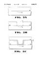
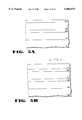
- LI 102may be a metal (e.g. titanium tungsten (TiW)) or a polysilicon gate member or other conductive material, such as a silicide, or doped polysilicon.
- the dielectric oxide layer 104is polished.
- a contact or a via 106 through the dielectric oxide 104is created by a suitable technique such as with a mask and etching, ending at the patterned LI 102.
- the next stepis to deposit an adhesive layer 108 over the dielectric oxide 104 and into the opening 106, without completely filling the opening 106.
- An adhesive layerhelps an overlying conductive layer adhere to dielectric oxide layer 104 and may itself be formed of a conductive material such as titanium.
- Wtungsten
- FIG. 1Fan etch back is performed on the conductive 110 layer but the etch is stopped at the adhesive layer 108. Thus, a portion of the surface of the conductive layer is exposed as shown in FIG. 1F.
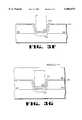
- a layer of a photoresist 114is deposited covering adhesive layer 108 and onto the exposed portion of conductor 110.
- a mask 112is used to pattern a local interconnect ("LI") 116 by etching the adhesive layer 108.
- the LI 116has been formed by adhesive layer 108 and stripping photoresist 114.
- FIG. 1Iillustrates a dielectric oxide layer 118 which has been deposited over dielectric oxide 104 and a contact formed such as by a mask and etch of dielectric oxide 118. The result is an opening 120 formed in the dielectric oxide layer 118.
- the contact surface of opening 120 in FIG. 1Iis often compromised due to insufficient cleaning of the bottom of the contact opening 120.
- LI 116is made of a material having a low melting point (e.g. titanium), it is difficult to heat treat the bottom of the contact opening 120 to remove contaminants without causing LI 116 to reflow. Difficulties in getting adhesive layer 122 to the bottom of the opening 120 can also occur, especially when an opening has a high aspect ratio.
- This methodis labor-intensive (i.e., two conductive material depositions and two etch-backs), thus increasing the possibility of error or contamination from the increased complexity of processing.
- the present inventionprovides a method of forming an interconnect, such as a contact, metal post or via to a region of an electronic device and a semiconductor comprising such an interconnect.
- an interconnectcomprising:
- Another embodiment of the inventionconcerns a method for forming an interconnect comprising:
- first conductive material structure and said second conductive material structuresubstantially fills said opening
- FIGS. 1A-1Jillustrate a conventional method of forming a metal post.
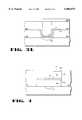
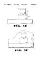
- FIG. 2illustrates a conductive material post that is formed according to a first embodiment of the present invention.
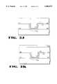
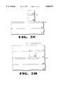
- FIGS. 3A-3Lillustrate steps for forming an interconnect according to a first embodiment of the present invention.
- FIG. 4illustrates an interconnect that is formed according to a second embodiment of the present invention.
- FIGS. 5A-5Jillustrate steps for forming an interconnect according to a second embodiment of the present invention.
- a method for forming an interconnect between regions of an electronic device using conductive materials in structuresis described.
- numerous detailsare set forth, such as the use of photoresist or the use of a self-aligned contact etch. It will be apparent, however, to one skilled in the art, that the present invention may be practiced other than as specifically described herein. In other instances, well-known structures and processes have not been set forth in detail in order to avoid obscuring the present invention.
- FIG. 2illustrates a conductive material post that was formed according to one embodiment of the present invention.
- the top surface 202 of a conductive material post 206(which may comprise, e.g., titanium, zirconium, hafnium, chromium, molybdenum, tungsten, alloys thereof such as titanium-tungsten, polysilicon, etc.) is exposed after an oxide polish or oxide etch step.
- the conductive materialis preferably tungsten.
- the conductive material post 206is shown surrounded by dielectric layers 208 and 210 (for example silicon dioxide, silicon nitride, oxide/nitride/oxide or SiO x N y ).
- the conductive material post 206makes contact to a substrate region 216 of an electronic device, such as a source or drain region of a MOS transistor, a gate material of a gate electrode, a conductive region of a local interconnect or a conductive material.
- the conductive material post 206may be aligned with the substrate region 216; however, conductive material post 206 does not necessarily have to be completely aligned with the substrate region 216 to which contact is made.
- an etch stop layer 214e.g. metals such as titanium, zirconium, hafnium, chromium, molybdenum, tungsten, alloys thereof such as titanium-tungsten; oxides, nitrides and oxynitrides of such metals or of Si, such as silicon dioxide, silicon nitride, silicon oxynitride, and silicides such as WSi x and TiSi x
- metalssuch as titanium, zirconium, hafnium, chromium, molybdenum, tungsten, alloys thereof such as titanium-tungsten; oxides, nitrides and oxynitrides of such metals or of Si, such as silicon dioxide, silicon nitride, silicon oxynitride, and silicides such as WSi x and TiSi x
- etch stop layer 214primarily prevents etchants from etching underlying layer of materials but may also form a local interconnect as well as
- An adhesive or glue layer 212(e.g titanium, zirconium, hafnium, chromium, molybdenum, tungsten, alloys thereof such as titanium-tungsten) may also be provided which assists adherence of an overlying etch stop and/or conductive material layer (e.g. metal such as tungsten or doped polysilicon) to an adjacent dielectric layer (e.g. an oxide, nitride or other dielectric).
- the upper portion of the conductive material post 206is not necessarily surrounded by an adhesive layer, but rather, may be surrounded by an insulating dielectric layer 208.
- the etch stop and/or the adhesive layermay also be made of a conductive material.
- FIGS. 3A--3Lillustrate one method for practicing the present invention.
- FIG. 3Aillustrates a dielectric layer 302 that has been deposited by a technique conventionally known to those of ordinary skill in the art for example by atmospheric pressure Chemical Vapor Deposition (APCVD), low pressure Chemical Vapor Deposition (LPCVD), plasma-enhance Chemical Vapor Deposition (EPCVD), sputtering or thermally grown.
- the thickness of dielectric layer 302is not particularly limited but preferably is in the range of about 0.3-3 ⁇ m, more preferably 0.5-1 ⁇ m.
- Dielectric layer 302overlies a substrate region 304 to which contact will be made.
- the substrate region 304is typically either a source or a drain region of a semiconductor substrate, a gate material of a gate electrode, a contact for a local interconnect or a conductive material.
- an opening 306 through dielectric layer 302 to substrate region 304 to which contact will be made,is made by conventional methods known to those of ordinary skill in the art such as by a self-aligned contact etch to form an opening. A non self-aligned mask may also be used.
- an etch stop layer 308(e.g., titanium, zirconium, hafnium, chromium, molybdenum, tungsten, alloys thereof such as titanium-tungsten alloy, etc.) is deposited over the dielectric layer 302 and into the opening 306, without completely filling the opening 306.
- the thickness of the etch stop layeris not particularly limited and generally ranges from 50-2,500 ⁇ , preferably 70-2,000 ⁇ , more preferably 100-1,500 ⁇ .
- a thicknessis preferably in the range of about 100-2,000 ⁇ , preferably 100-1,500 ⁇ , more preferably 120-1,200 ⁇ .
- conductors or metalsmay be used as an etch stop layer besides titanium, titanium tungsten alloy or Cr in the present invention, provided that the etch stop layer is sufficiently resistant to etching under the selected etching conditions to allow for selectively etching the conductive material layer 312 at a greater rate relative to the rate of etching of the dielectric layer 302.
- the etch stop materialit is also possible to use nitrides such as silicon nitride, especially when the conductive material layer is tungsten.
- adhesive layer 310e.g. titanium, zirconium, hafnium, chromium, molybdenum, tungsten, copper, silver, gold, platinum, alloys thereof such as titanium-tungsten alloy, etc.
- the thickness of the adhesive layeris not particularly limited and generally ranges from 50-2,500 ⁇ .
- a thicknessis preferably in the range of approximately 400-1,500 ⁇ .
- a stuffing stepmay be used after the etch stop layer 308 and optional adhesive layer 310 have been deposited.
- This stuffing stepis a heat treatment to get better contact resistance and better resistance to the conductive material deposition.
- a layer of conductive material 312is deposited that substantially fills the contact opening 306.
- the thickness of the conductive material layermay vary depending on the desired height of the conductive material post, but is preferably of a thickness of about 0.4-4.0 ⁇ m, preferably 0.5-3.0 ⁇ m, more preferably 0.7-2.5 ⁇ m.
- Non-limiting examples of conductive materialsare titanium, zirconium, hafnium, chromium, molybdenum, tungsten, alloys thereof such as titanium-tungsten alloy etc. aluminum and polysilicon.
- the conductive material layeris tungsten.
- the present inventionmay advantageously deposit one conductive material layer.
- the present inventionprovides a more streamlined and cost-efficient method for forming a conductive material post.
- a metal contact mask 314is used to pattern a layer of deposited photoresist 316.
- a reverse metal contact mask and positive photoresist systemis illustrated in FIG. D, however those of ordinary skill in the art will appreciate that masking can be accomplished with a metal contact mask and negative photoresist system. Exemplary positive and negative photoresist systems are described later in this application. It is to be appreciated that other conventional techniques may be used to pattern the photoresist or to etch the conductive material 312.
- the photoresist 316is developed by conventional methods know to those of ordinary skill in the art.
- the conductive material 312is preferably anisotropically etched as illustrated in FIG. 3E.
- control of lateral etchingduring formation of the conductive material post 318.
- Control of lateral etchingmay be obtained by conventionally maintaining a low wafer electrode temperature of about 10° C. and by introducing N 2 gas or a polymer forming gas, such as CHF 3 , into the etch chamber for sidewall passivation.
- the protocol of this preferred embodimentresults in a conductive material post 318 with a layer of photoresist 316 on top of it.
- Another advantage of the present inventionis that it only requires one conductive material etch, unlike other methods which required two etches. This reduces the possibility of contamination and defects due to contamination during the etching process.
- adhesive layer 310may also be etched, either during the etch of the conductive material or in a separate etch step.
- the photoresist 316is stripped and a conductive material post 318 is shown protruding above etch stop layer 308, adhesive layer 310 and dielectric layer 302 as shown in FIG. 3F.
- etch stop layer 308may be patterned into a local interconnect.
- the local interconnectis formed such that there is an axis normal to said semiconductor substrate which passes through said etch stop layer but does not pass through said conductive material structure.
- a local interconnectmay serve to electrically connect a second contact or via to an additional metal line. It is sometimes desirable to provide multiple points of electrical connection to a substrate region, such as when two or more parallel planes of perpendicular metal lines are used to provide a conductive network across a plane of an integrated circuit.
- a layer of photoresist 322is deposited around the conductive material post 318.
- a local interconnect mask 320is used to pattern a photoresist 322 and etch stop layer 308. It is to be appreciated that the local interconnect may be formed using other conventional techniques.
- the photoresist 322is developed and a local interconnect ("LI") 324 is etched and formed from the adhesive layer 308 of FIG. 3G. The remaining photoresist 322 is then stripped.
- LIlocal interconnect
- a layer of dielectric 326is deposited using any of the conventional techniques, such as sputtering or chemical vapor deposition.
- the dielectric layer 326is polished to expose the top layer of conductive material post 318 as described in FIG. 3J.
- Dielectric layer 326may be planarized utilizing techniques other than polishing.
- a metallization layer of a conductor 328such as aluminum, is deposited over the dielectric layer 326.
- metallization layer 328has been patterned using a mask or any other conventional technique to form a local interconnect ("LI”) 330.
- metallization layer 328is not necessarily drawn to scale and in actuality, may be almost as thick as dielectric layer 326.
- FIG. 4illustrates an interconnect that was formed according to a second embodiment of the present invention.
- Non-limiting examples of a regioninclude a source or a drain region of a substrate, a gate material of a gate electrode, a metallization layer or a local interconnect.
- the first conductive structureis a conductive material post 413 comprising a conductive material layer 407, optionally comprising a cap 409 such as chromium.
- the conductive material layer 407may preferably be a metal such as aluminum, doped polysilicon, titanium, zirconium, hafnium, chromium, molybdenum, tungsten, copper, silver, gold, platinum, conductive alloys thereof such as titanium-tungsten alloy etc., more preferably aluminum.
- the cap 409may also be made of aluminum, silicon, titanium, zirconium, hafnium, chromium, molybdenum, tungsten, copper, silver, gold, platinum, conductive alloys thereof such as titanium-tungsten alloy, and is preferably a titanium tungsten alloy.
- a second conductive structure 415is formed from, in one embodiment, a conductive material layer 403 such as aluminum, doped polysilicon, titanium, zirconium, hafnium, chromium, molybdenum, tungsten, copper, silver, gold, platinum, conductive alloys thereof such as titanium-tungsten alloy, aluminum, preferably aluminum and a etch stop layer 405 such as titanium, zirconium, hafnium, chromium, molybdenum, tungsten, alloys thereof such as titanium-tungsten alloy, preferably titanium tungsten alloy. If the cap 409 is made of titanium tungsten alloy, etch stop layer 405 may be made of chromium.
- the conductive material posts 413 and 415are surrounded by an insulating dielectric layer 401, such as silicon dioxide, silicon nitride, a conventional oxide/nitride/oxide or Si x N y . although conductive material posts 413 and 415 are shown as being aligned along one edge, they do not necessarily have to be aligned as shown in FIG. 4. The top surface 411 of cap 409 is exposed and is ready to make contact to another conductive material layer.
- an insulating dielectric layer 401such as silicon dioxide, silicon nitride, a conventional oxide/nitride/oxide or Si x N y .
- FIGS. 5A-5Jillustrate the steps for preparing a conducting means according to a second embodiment of the present invention.
- Substrate layer 501contains a substrate region to which contact is made.
- substrate regionsare a source or a drain region of a substrate, a gate material of a gate electrode, a metallization layer or a local interconnect.
- the above-identified substrate regionsare typically only a portion of the substrate layer 501, the remaining material typically being a dielectric material such as silicon dioxide, silicon nitride, a conventional oxide/nitride/oxide or SiO x N y .
- conductive material 502 and 506are illustrated.
- conductive materialare titanium, zirconium, hafnium, chromium, molybdenum, tungsten, alloys thereof such as titanium-tungsten alloy, polysilicon, aluminum, aluminum alloys, tungsten silicide, a silicide, a salicide, a polycide, a doped polysilicon etc.
- the conductive material layers 502 and 506are aluminum.
- etch stop layer 504is illustrated.
- etch stop layerincluding chromium, titanium-tungsten alloy, and others as mentioned above.
- the etch stop layer 504may provide an adhesive interface between conductive material layers 502 and 506 and acts as an etch stop during the formation of a first conductive material post.
- the etch stop layer 504is most preferably sufficiently resistant to etching, under the selected etching conditions, to allow for etching of a conductive material layer 506 and optional cap layer 508 without substantially etching the conductive material layer 502.
- the etch stop materialis etched more slowly than the overlying layer(s) being etched, preferably at a relative rate selectivity of ⁇ 1:2, more preferably ⁇ 1:5.
- adhesive layer 508is illustrated.
- adhesive layerinclude chromium, titanium-tungsten alloy and others as indicated above.
- Adhesive layer 504in particular provides an adhesive interface between conductive material layers 502 and 506 and may act as an etch stop during the formation of a first conductive material post.
- resist layers 510, 514 and 516are illustrated.
- Negative resist materialsmay contain chemically inert polymer components such as rubber and/or photoreactive agents that react with light to form cross-links, e.g. with the rubber. When placed in an organic developer solvent, the unexposed and unpolymerized resist dissolves, leaving a polymeric pattern in the exposed regions.
- suitable negative resist materialsinclude cresol epoxy novolac-based negative resists as well as negative resists containing the photoreactive polymers described in Kirk-Othmer Encyclopedia of Chemical Technology, 3rd Edition, vol 17, entitled “Photoreactive Polymers", pages 680-708, the relevant portions of which are hereby incorporated by references.
- Positive resistshave photoreactive components which are destroyed in the regions exposed to light. Typically the resist is removed in an aqueous alkaline solution, where the exposed region dissolves away.
- suitable positive resist materialsare within the level of skill of one of ordinary skill in the art without undue experimentation.
- Specific non-limiting examples of suitable positive resist systemsinclude Shipley XP9402, JSR KRK-K2G and JSR KRF-L7 positive resists as well as positive resists containing the photoreactive polymers described in Kirk-Othmer Encyclopedia of Chemical Technology, 3rd Edition, vol 17, entitled “Photoreactive Polymers", pages 680-708, the relevant portions of which are hereby incorporated by references.
- Exemplary resist materialsare also described by Bayer et al, IBM Tech. Discl. Bull (USA) vol 22, No 5 October 1979 pp 1855; Tabei, U.S. Pat. No. 4,613,404; Taylor et al, J. Vac. Sci, Technol. B. Vol 13, No. 6, 95 pp 3078-3081; Argitis et al, J. Vac. Sci, Technol. B. Vol 13, No. 6, 95 pp 3030-3034; Itani et al, J. Vac. Sci, Technol. B. Vol 13, No. 6, 95 pp 3026-3029; Ohfuji et al, J. Vac. Sci, Technol. B. Vol 13, No.
- dielectric layer 522is illustrated.
- dielectric materialare silicon dioxide, silicon nitride, a conventional oxide/nitride/oxide, tetraorthosilicate based oxides, titanium oxide and SiO x N y .
- a first conductive material layer 502such as aluminum that is about 1 ⁇ m thick in one embodiment is deposited on a substrate layer 501.
- the substrate layer 501may have an opening in it or, a metal line or a local interconnect under it such that it will connect the first conductive material layer 502 to another region underneath the substrate layer 501.
- an opening in substrate layer 501may expose an underlying interconnect such as interconnect 108 shown in FIG. 1D.
- the first conductive material layer 502may be deposited such as by a sputtering.
- an etch stop layer 504such as of titanium tungsten alloy that is about 1,000 ⁇ thick is deposited.
- another layer of conductive material 506such as aluminum that is about 1 micron thick is deposited over etch stop layer 504.
- adhesive layer 508such as of titanium tungsten alloy that is about 1,500 ⁇ thick is deposited over the conductive material layer 506.
- the conductive material layer 502, the etch stop layer 504, the conductive material layer 506, and the adhesive layer 508are sputter deposited in one pass through a sputter deposition processing equipment. It is to be appreciated that these layers may also be formed using other conventional techniques and that these layers may be of different conductive materials and different thicknesses without departing from the spirit and scope of the present invention.
- a layer of photoresist 510is deposited over the top layer of adhesive layer 508.
- a post mask 511is then applied and etched to form a first conductive material post.
- the photoresist 510is developed and a fluorine etch may be used to etch the top layer of adhesive layer 508, when adhesive layer 508 is chromium or titanium-tungsten alloy.
- a chlorine etchmay be used to etch conductive material (e.g., aluminum) layer 506, stopping at etch stop layer 504 when conductive material layer 506 is aluminum and etch stop layer 504 is titanium-tungsten alloy.
- Etch stop layer 504 and adhesive layer 508may be thinned during the etch of conductive material layer 506.
- this or any conductive material layermay be conventionally polished, such as by chemical mechanical polishing.
- etch stop layer 504 and optional adhesive layer 508may be selected in accordance with the etching process used such that etching of the conductive material 506, and adhesive layer 508 when present is conducted in the substantial absence of etching of conductive layer 502, preferably in the substantial absence of etching of the etch stop layer 504.
- a metal pattern resistis then applied to form a second conductive material post.
- Metal mask 512is used to pattern the conductive material post.
- the length of metal mask 512is preferably greater than the length of mask 511 such that an axis normal to said substrate may pass through said second conductive material post without passing through said first conductive material post.
- a mask 511 and a metal mask 512was used, other conventional techniques may be used to pattern a conductive material post.
- the photoresistmay be applied in two different ways. The photoresist may be applied as shown in area 516 such that the top adhesive layer 508 is exposed during the etch of etch stop layer 504 and conductive material layer 502. On the other hand, the positive photoresist may be applied so as to cover the adhesive layer 508 as shown in area 514 and area 516.
- Etch stop layer 504may be etched using fluorine and conductive material layer 502 is etched using chlorine to produce the structure shown in FIG. 5E when etch stop layer is titanium-tungsten alloy and conductive material layer is aluminum. The chlorine etch stops on substrate layer 501. The result is a conductive material post 520 which is formed below conductive material post 518 that was formed from the earlier etch, as illustrated in FIG. 5C. The result is a multidimensional interconnect to which multiple sites of attachment are possible.
- etch stop layer 504 and substrate layer 501may be selected in accordance with the etching process and etchant used such that etching of the conductive material layer 502 is conducted in the substantial absence of etching of the substrate layer 501.
- the next step, as illustrated in FIG. 5F,is to deposit an insulating dielectric layer, such as a blanket layer of dielectric 522 over the semiconductor substrate.
- an insulating dielectric layersuch as a blanket layer of dielectric 522 over the semiconductor substrate.
- the dielectric 522is polished or planarized using conventional techniques so that a surface 524 of the top layer of adhesive layer 508 is exposed. It is to be appreciated that this top adhesive layer 508 may be replaced with chromium in a preferred embodiment.
- a second conductive material layer 526is deposited over the structure shown in FIG. 5G.
- a layer of photoresist 528has been deposited over the layer of conductive material 526.
- conductive material 526is preferably a metal such as aluminum.
- aluminummay be replaced by a different metal or a conductive non-metal.
- a mask or any other conventional meansis used to pattern and develop the photoresist 528 and etch conductive material layer 526 to form a conductive structure, such as an interconnect.
- FIG. 5Jthe photoresist 528 is stripped and a conductive material structure 526 is formed which can then be used to connect conductive material post 518 and conductive material post 520 to another conductive structure.
Landscapes
- Engineering & Computer Science (AREA)
- Physics & Mathematics (AREA)
- Condensed Matter Physics & Semiconductors (AREA)
- General Physics & Mathematics (AREA)
- Computer Hardware Design (AREA)
- Microelectronics & Electronic Packaging (AREA)
- Power Engineering (AREA)
- Manufacturing & Machinery (AREA)
- Internal Circuitry In Semiconductor Integrated Circuit Devices (AREA)
Abstract
Description
Claims (8)
Priority Applications (1)
| Application Number | Priority Date | Filing Date | Title |
|---|---|---|---|
| US08/672,050US6004874A (en) | 1996-06-26 | 1996-06-26 | Method for forming an interconnect |
Applications Claiming Priority (1)
| Application Number | Priority Date | Filing Date | Title |
|---|---|---|---|
| US08/672,050US6004874A (en) | 1996-06-26 | 1996-06-26 | Method for forming an interconnect |
Publications (1)
| Publication Number | Publication Date |
|---|---|
| US6004874Atrue US6004874A (en) | 1999-12-21 |
Family
ID=24696949
Family Applications (1)
| Application Number | Title | Priority Date | Filing Date |
|---|---|---|---|
| US08/672,050Expired - LifetimeUS6004874A (en) | 1996-06-26 | 1996-06-26 | Method for forming an interconnect |
Country Status (1)
| Country | Link |
|---|---|
| US (1) | US6004874A (en) |
Cited By (20)
| Publication number | Priority date | Publication date | Assignee | Title |
|---|---|---|---|---|
| US6171954B1 (en)* | 1998-06-12 | 2001-01-09 | United Microelectronics Corp. | Method of manufacturing self-aligned contact |
| US6232224B1 (en)* | 1999-04-20 | 2001-05-15 | Nec Corporation | Method of manufacturing semiconductor device having reliable contact structure |
| US6258709B1 (en)* | 2000-06-07 | 2001-07-10 | Micron Technology, Inc. | Formation of electrical interconnect lines by selective metal etch |
| WO2002023627A1 (en)* | 2000-09-14 | 2002-03-21 | Infineon Technologies North America Corp. | Semiconductor interconnection structure and method of fabrication |
| WO2002023626A1 (en)* | 2000-09-14 | 2002-03-21 | Infineon Technologies North America Corp. | Improved semiconductor structure and method of fabrication |
| US6423644B1 (en) | 2000-07-12 | 2002-07-23 | Applied Materials, Inc. | Method of etching tungsten or tungsten nitride electrode gates in semiconductor structures |
| US6440870B1 (en) | 2000-07-12 | 2002-08-27 | Applied Materials, Inc. | Method of etching tungsten or tungsten nitride electrode gates in semiconductor structures |
| US6613687B2 (en)* | 2001-03-28 | 2003-09-02 | Lexmark International, Inc. | Reverse reactive ion patterning of metal oxide films |
| US20040071034A1 (en)* | 2002-06-27 | 2004-04-15 | Vyvoda Michael A. | Electrically isolated pillars in active devices |
| US20040110318A1 (en)* | 1999-04-19 | 2004-06-10 | Murata Manufacturing Co., Ltd. | Method of manufacturing an external force detection sensor |
| US6756315B1 (en) | 2000-09-29 | 2004-06-29 | Cypress Semiconductor Corporation | Method of forming contact openings |
| US20040197966A1 (en)* | 2003-04-03 | 2004-10-07 | Heung-Lyul Cho | Manufacturing method of liquid crystal display device |
| US20040266206A1 (en)* | 2003-06-30 | 2004-12-30 | Matrix Semiconductor, Inc. | Post vertical interconnects formed with silicide etch stop and method of making |
| US20080296778A1 (en)* | 2007-05-30 | 2008-12-04 | Qimonda Ag | Interconnection Structure and Integrated Circuit |
| US20090224244A1 (en)* | 2005-02-17 | 2009-09-10 | Sandisk 3D Llc | Patterning of submicron pillars in a memory array |
| US20120211721A1 (en)* | 2011-02-23 | 2012-08-23 | Kabushiki Kaisha Toshiba | Semiconductor storage device and manufacturing method thereof |
| US8399360B1 (en) | 2005-11-17 | 2013-03-19 | Cypress Semiconductor Corporation | Process for post contact-etch clean |
| US8927869B2 (en) | 2012-04-11 | 2015-01-06 | International Business Machines Corporation | Semiconductor structures and methods of manufacture |
| US20160064610A1 (en)* | 2013-05-14 | 2016-03-03 | Osram Opto Semiconductors Gmbh | Optoelectronic Device and Method for Producing Same |
| US20220246557A1 (en)* | 2021-06-30 | 2022-08-04 | Shennan Circuits Co., Ltd. | Package chip and method of manufacturing the same, rewiring package chip and method of manufacturing the same |
Citations (20)
| Publication number | Priority date | Publication date | Assignee | Title |
|---|---|---|---|---|
| US4410622A (en)* | 1978-12-29 | 1983-10-18 | International Business Machines Corporation | Forming interconnections for multilevel interconnection metallurgy systems |
| US4536951A (en)* | 1983-06-16 | 1985-08-27 | Plessey Overseas Limited | Method of producing a layered structure |
| US4624864A (en)* | 1984-06-14 | 1986-11-25 | Commissariat A L'energie Atomique | Process for the autopositioning of an interconnection line on an electric contact hole of an integrated circuit |
| EP0242893A1 (en)* | 1986-03-26 | 1987-10-28 | Koninklijke Philips Electronics N.V. | Method of manufacturing a semiconductor device |
| US4711701A (en)* | 1986-09-16 | 1987-12-08 | Texas Instruments Incorporated | Self-aligned transistor method |
| EP0303061A2 (en)* | 1987-08-13 | 1989-02-15 | International Business Machines Corporation | Process for forming a planarized, metal-strapped polysilicon gate FET |
| US4824521A (en)* | 1987-04-01 | 1989-04-25 | Fairchild Semiconductor Corporation | Planarization of metal pillars on uneven substrates |
| US4866008A (en)* | 1987-12-11 | 1989-09-12 | Texas Instruments Incorporated | Methods for forming self-aligned conductive pillars on interconnects |
| US4892835A (en)* | 1987-03-24 | 1990-01-09 | U.S. Philips Corporation | Method of manufacturing a field effect transistor |
| US4914056A (en)* | 1985-05-13 | 1990-04-03 | Kabushiki Kaisha Toshiba | Method of manufacturing a semiconductor device having tapered pillars |
| US4917759A (en)* | 1989-04-17 | 1990-04-17 | Motorola, Inc. | Method for forming self-aligned vias in multi-level metal integrated circuits |
| US4954423A (en)* | 1985-08-06 | 1990-09-04 | Texas Instruments Incorporated | Planar metal interconnection for a VLSI device |
| US4996133A (en)* | 1987-07-31 | 1991-02-26 | Texas Instruments Incorporated | Self-aligned tungsten-filled via process and via formed thereby |
| US5065208A (en)* | 1987-01-30 | 1991-11-12 | Texas Instruments Incorporated | Integrated bipolar and CMOS transistor with titanium nitride interconnections |
| US5166771A (en)* | 1990-01-12 | 1992-11-24 | Paradigm Technology, Inc. | Self-aligning contact and interconnect structure |
| US5219784A (en)* | 1990-04-02 | 1993-06-15 | National Semiconductor Corporation | Spacer formation in a bicmos device |
| US5258096A (en)* | 1992-08-20 | 1993-11-02 | Micron Semiconductor, Inc. | Method of forming local etch stop landing pads for simultaneous, self-aligned dry etching of contact vias with various depths |
| US5385634A (en)* | 1990-04-05 | 1995-01-31 | Ramtron International Corporation | Sealed self aligned contact process |
| US5436199A (en)* | 1988-02-26 | 1995-07-25 | Texas Instruments Incorporated | Pillar alignment and formation process |
| US5514622A (en)* | 1994-08-29 | 1996-05-07 | Cypress Semiconductor Corporation | Method for the formation of interconnects and landing pads having a thin, conductive film underlying the plug or an associated contact of via hole |
- 1996
- 1996-06-26USUS08/672,050patent/US6004874A/ennot_activeExpired - Lifetime
Patent Citations (20)
| Publication number | Priority date | Publication date | Assignee | Title |
|---|---|---|---|---|
| US4410622A (en)* | 1978-12-29 | 1983-10-18 | International Business Machines Corporation | Forming interconnections for multilevel interconnection metallurgy systems |
| US4536951A (en)* | 1983-06-16 | 1985-08-27 | Plessey Overseas Limited | Method of producing a layered structure |
| US4624864A (en)* | 1984-06-14 | 1986-11-25 | Commissariat A L'energie Atomique | Process for the autopositioning of an interconnection line on an electric contact hole of an integrated circuit |
| US4914056A (en)* | 1985-05-13 | 1990-04-03 | Kabushiki Kaisha Toshiba | Method of manufacturing a semiconductor device having tapered pillars |
| US4954423A (en)* | 1985-08-06 | 1990-09-04 | Texas Instruments Incorporated | Planar metal interconnection for a VLSI device |
| EP0242893A1 (en)* | 1986-03-26 | 1987-10-28 | Koninklijke Philips Electronics N.V. | Method of manufacturing a semiconductor device |
| US4711701A (en)* | 1986-09-16 | 1987-12-08 | Texas Instruments Incorporated | Self-aligned transistor method |
| US5065208A (en)* | 1987-01-30 | 1991-11-12 | Texas Instruments Incorporated | Integrated bipolar and CMOS transistor with titanium nitride interconnections |
| US4892835A (en)* | 1987-03-24 | 1990-01-09 | U.S. Philips Corporation | Method of manufacturing a field effect transistor |
| US4824521A (en)* | 1987-04-01 | 1989-04-25 | Fairchild Semiconductor Corporation | Planarization of metal pillars on uneven substrates |
| US4996133A (en)* | 1987-07-31 | 1991-02-26 | Texas Instruments Incorporated | Self-aligned tungsten-filled via process and via formed thereby |
| EP0303061A2 (en)* | 1987-08-13 | 1989-02-15 | International Business Machines Corporation | Process for forming a planarized, metal-strapped polysilicon gate FET |
| US4866008A (en)* | 1987-12-11 | 1989-09-12 | Texas Instruments Incorporated | Methods for forming self-aligned conductive pillars on interconnects |
| US5436199A (en)* | 1988-02-26 | 1995-07-25 | Texas Instruments Incorporated | Pillar alignment and formation process |
| US4917759A (en)* | 1989-04-17 | 1990-04-17 | Motorola, Inc. | Method for forming self-aligned vias in multi-level metal integrated circuits |
| US5166771A (en)* | 1990-01-12 | 1992-11-24 | Paradigm Technology, Inc. | Self-aligning contact and interconnect structure |
| US5219784A (en)* | 1990-04-02 | 1993-06-15 | National Semiconductor Corporation | Spacer formation in a bicmos device |
| US5385634A (en)* | 1990-04-05 | 1995-01-31 | Ramtron International Corporation | Sealed self aligned contact process |
| US5258096A (en)* | 1992-08-20 | 1993-11-02 | Micron Semiconductor, Inc. | Method of forming local etch stop landing pads for simultaneous, self-aligned dry etching of contact vias with various depths |
| US5514622A (en)* | 1994-08-29 | 1996-05-07 | Cypress Semiconductor Corporation | Method for the formation of interconnects and landing pads having a thin, conductive film underlying the plug or an associated contact of via hole |
Non-Patent Citations (2)
| Title |
|---|
| Lee, et al., "A Process Technology For 1 Giga-Bit Dram", IEDM Tech. Dig, Dec. 1995, pp. 907-910. |
| Lee, et al., A Process Technology For 1 Giga Bit Dram , IEDM Tech. Dig, Dec. 1995, pp. 907 910.* |
Cited By (41)
| Publication number | Priority date | Publication date | Assignee | Title |
|---|---|---|---|---|
| US6171954B1 (en)* | 1998-06-12 | 2001-01-09 | United Microelectronics Corp. | Method of manufacturing self-aligned contact |
| US7067344B1 (en)* | 1999-04-19 | 2006-06-27 | Murata Manufacturing Co., Ltd. | Method of manufacturing an external force detection sensor |
| US7393714B2 (en) | 1999-04-19 | 2008-07-01 | Murata Manufacturing Co., Ltd. | Method of manufacturing external force detection sensor |
| US20060110843A1 (en)* | 1999-04-19 | 2006-05-25 | Takahiro Oguchi | Method of manufacturing an external force detection sensor |
| US20040110318A1 (en)* | 1999-04-19 | 2004-06-10 | Murata Manufacturing Co., Ltd. | Method of manufacturing an external force detection sensor |
| US7049165B2 (en) | 1999-04-19 | 2006-05-23 | Murata Manufacturing Co., Ltd. | Method of manufacturing an external force detection sensor |
| US6232224B1 (en)* | 1999-04-20 | 2001-05-15 | Nec Corporation | Method of manufacturing semiconductor device having reliable contact structure |
| US6258709B1 (en)* | 2000-06-07 | 2001-07-10 | Micron Technology, Inc. | Formation of electrical interconnect lines by selective metal etch |
| US6440870B1 (en) | 2000-07-12 | 2002-08-27 | Applied Materials, Inc. | Method of etching tungsten or tungsten nitride electrode gates in semiconductor structures |
| US6579806B2 (en) | 2000-07-12 | 2003-06-17 | Applied Materials Inc. | Method of etching tungsten or tungsten nitride in semiconductor structures |
| US6423644B1 (en) | 2000-07-12 | 2002-07-23 | Applied Materials, Inc. | Method of etching tungsten or tungsten nitride electrode gates in semiconductor structures |
| WO2002023626A1 (en)* | 2000-09-14 | 2002-03-21 | Infineon Technologies North America Corp. | Improved semiconductor structure and method of fabrication |
| WO2002023627A1 (en)* | 2000-09-14 | 2002-03-21 | Infineon Technologies North America Corp. | Semiconductor interconnection structure and method of fabrication |
| US6756315B1 (en) | 2000-09-29 | 2004-06-29 | Cypress Semiconductor Corporation | Method of forming contact openings |
| US6613687B2 (en)* | 2001-03-28 | 2003-09-02 | Lexmark International, Inc. | Reverse reactive ion patterning of metal oxide films |
| US20040087072A1 (en)* | 2002-06-27 | 2004-05-06 | Vyvoda Michael A. | Electrically isolated pillars in active devices |
| US6952043B2 (en) | 2002-06-27 | 2005-10-04 | Matrix Semiconductor, Inc. | Electrically isolated pillars in active devices |
| US7413945B2 (en) | 2002-06-27 | 2008-08-19 | Sandisk 3D Llc | Electrically isolated pillars in active devices |
| US20040071034A1 (en)* | 2002-06-27 | 2004-04-15 | Vyvoda Michael A. | Electrically isolated pillars in active devices |
| US7245000B2 (en) | 2002-06-27 | 2007-07-17 | Sandisk Corporation | Electrically isolated pillars in active devices |
| US7256076B2 (en)* | 2003-04-03 | 2007-08-14 | Lg.Philips Lcd Co., Ltd. | Manufacturing method of liquid crystal display device |
| US20040197966A1 (en)* | 2003-04-03 | 2004-10-07 | Heung-Lyul Cho | Manufacturing method of liquid crystal display device |
| US20080029901A1 (en)* | 2003-06-30 | 2008-02-07 | Cleeves James M | Post vertical interconnects formed with silicide etch stop and method of making |
| US20040266206A1 (en)* | 2003-06-30 | 2004-12-30 | Matrix Semiconductor, Inc. | Post vertical interconnects formed with silicide etch stop and method of making |
| US7307012B2 (en) | 2003-06-30 | 2007-12-11 | Sandisk 3D Llc | Post vertical interconnects formed with silicide etch stop and method of making |
| US7768038B2 (en) | 2003-06-30 | 2010-08-03 | Sandisk 3D Llc | Post vertical interconnects formed with silicide etch stop and method of making |
| US8759176B2 (en) | 2005-02-17 | 2014-06-24 | Sandisk 3D Llc | Patterning of submicron pillars in a memory array |
| US20090224244A1 (en)* | 2005-02-17 | 2009-09-10 | Sandisk 3D Llc | Patterning of submicron pillars in a memory array |
| US8399360B1 (en) | 2005-11-17 | 2013-03-19 | Cypress Semiconductor Corporation | Process for post contact-etch clean |
| DE102007032269A1 (en)* | 2007-05-30 | 2008-12-04 | Qimonda Ag | Connection structure and integrated circuit |
| US20080296778A1 (en)* | 2007-05-30 | 2008-12-04 | Qimonda Ag | Interconnection Structure and Integrated Circuit |
| DE102007032269B4 (en)* | 2007-05-30 | 2014-07-10 | Qimonda Ag | Connection structure and integrated circuit and method for their production |
| DE102007063844B3 (en)* | 2007-05-30 | 2014-11-20 | Qimonda Ag | Integrated circuit and method for its production, electronic system |
| US20120211721A1 (en)* | 2011-02-23 | 2012-08-23 | Kabushiki Kaisha Toshiba | Semiconductor storage device and manufacturing method thereof |
| US8772754B2 (en)* | 2011-02-23 | 2014-07-08 | Kabushiki Kaisha Toshiba | Semiconductor storage device comprising a memory cell array including a rectifying element and a variable resistor |
| US8927869B2 (en) | 2012-04-11 | 2015-01-06 | International Business Machines Corporation | Semiconductor structures and methods of manufacture |
| US9230929B2 (en) | 2012-04-11 | 2016-01-05 | Globalfoundries Inc. | Semiconductor structures and methods of manufacture |
| US20160064610A1 (en)* | 2013-05-14 | 2016-03-03 | Osram Opto Semiconductors Gmbh | Optoelectronic Device and Method for Producing Same |
| US9882090B2 (en)* | 2013-05-14 | 2018-01-30 | Osram Opto Semiconductors Gmbh | Method for producing an optoelectronic device with a contact area of accurately and reproducibily defined size |
| US10026871B2 (en) | 2013-05-14 | 2018-07-17 | Osram Opto Semiconductors Gmbh | Method for producing an optoelectronic device with a contact area of accurately and reproducibly defined size |
| US20220246557A1 (en)* | 2021-06-30 | 2022-08-04 | Shennan Circuits Co., Ltd. | Package chip and method of manufacturing the same, rewiring package chip and method of manufacturing the same |
Similar Documents
| Publication | Publication Date | Title |
|---|---|---|
| US6004874A (en) | Method for forming an interconnect | |
| US4948459A (en) | Method of enabling electrical connection to a substructure forming part of an electronic device | |
| US5872385A (en) | Conductive interconnect structure and method of formation | |
| US4917759A (en) | Method for forming self-aligned vias in multi-level metal integrated circuits | |
| US6495452B1 (en) | Method to reduce capacitance for copper interconnect structures | |
| US4824803A (en) | Multilayer metallization method for integrated circuits | |
| US6016012A (en) | Thin liner layer providing reduced via resistance | |
| US5838051A (en) | Tungsten policide contacts for semiconductor devices | |
| US7960240B1 (en) | System and method for providing a dual via architecture for thin film resistors | |
| US6187663B1 (en) | Method of optimizing device performance via use of copper damascene structures, and HSQ/FSG, hybrid low dielectric constant materials | |
| EP1235264A2 (en) | Direct etch for thin film resistor using a hard mask | |
| US5654216A (en) | Formation of a metal via structure from a composite metal layer | |
| EP0388862B1 (en) | Fabrication method of a semiconductor device having a planarized surface | |
| US5641710A (en) | Post tungsten etch back anneal, to improve aluminum step coverage | |
| US5895975A (en) | Optimized process for creating and passivating a metal pillar via structure located between two metal interconnect structures | |
| US7808048B1 (en) | System and method for providing a buried thin film resistor having end caps defined by a dielectric mask | |
| US5057186A (en) | Method of taper-etching with photoresist adhesion layer | |
| US6350682B1 (en) | Method of fabricating dual damascene structure using a hard mask | |
| EP1183724A1 (en) | A method of manufacturing a semiconductor device | |
| US4855252A (en) | Process for making self-aligned contacts | |
| US5897374A (en) | Vertical via/contact with undercut dielectric | |
| EP0405660B1 (en) | A method of manufacturing a semiconductor device | |
| US6667217B1 (en) | Method of fabricating a damascene copper inductor structure using a sub-0.18 um CMOS process | |
| US20020030277A1 (en) | Novel self-aligned, low contact resistance, via fabrication process | |
| JP2002299437A (en) | Method for manufacturing semiconductor device |
Legal Events
| Date | Code | Title | Description |
|---|---|---|---|
| AS | Assignment | Owner name:CYPRESS SEMICONDUCTOR CORPORATION, CALIFORNIA Free format text:ASSIGNMENT OF ASSIGNORS INTEREST;ASSIGNOR:CLEEVES, JAMES M.;REEL/FRAME:008149/0373 Effective date:19960911 | |
| STCF | Information on status: patent grant | Free format text:PATENTED CASE | |
| FPAY | Fee payment | Year of fee payment:4 | |
| FPAY | Fee payment | Year of fee payment:8 | |
| FEPP | Fee payment procedure | Free format text:PAYER NUMBER DE-ASSIGNED (ORIGINAL EVENT CODE: RMPN); ENTITY STATUS OF PATENT OWNER: LARGE ENTITY Free format text:PAYOR NUMBER ASSIGNED (ORIGINAL EVENT CODE: ASPN); ENTITY STATUS OF PATENT OWNER: LARGE ENTITY | |
| FPAY | Fee payment | Year of fee payment:12 | |
| AS | Assignment | Owner name:MORGAN STANLEY SENIOR FUNDING, INC., NEW YORK Free format text:SECURITY INTEREST;ASSIGNORS:CYPRESS SEMICONDUCTOR CORPORATION;SPANSION LLC;REEL/FRAME:035240/0429 Effective date:20150312 | |
| AS | Assignment | Owner name:CYPRESS SEMICONDUCTOR CORPORATION, CALIFORNIA Free format text:PARTIAL RELEASE OF SECURITY INTEREST IN PATENTS;ASSIGNOR:MORGAN STANLEY SENIOR FUNDING, INC., AS COLLATERAL AGENT;REEL/FRAME:039708/0001 Effective date:20160811 Owner name:SPANSION LLC, CALIFORNIA Free format text:PARTIAL RELEASE OF SECURITY INTEREST IN PATENTS;ASSIGNOR:MORGAN STANLEY SENIOR FUNDING, INC., AS COLLATERAL AGENT;REEL/FRAME:039708/0001 Effective date:20160811 | |
| AS | Assignment | Owner name:MORGAN STANLEY SENIOR FUNDING, INC., NEW YORK Free format text:CORRECTIVE ASSIGNMENT TO CORRECT THE 8647899 PREVIOUSLY RECORDED ON REEL 035240 FRAME 0429. ASSIGNOR(S) HEREBY CONFIRMS THE SECURITY INTERST;ASSIGNORS:CYPRESS SEMICONDUCTOR CORPORATION;SPANSION LLC;REEL/FRAME:058002/0470 Effective date:20150312 |