US6004437A - Thin-film magnetic recording head manufacturing method - Google Patents
Thin-film magnetic recording head manufacturing methodDownload PDFInfo
- Publication number
- US6004437A US6004437AUS08/810,837US81083797AUS6004437AUS 6004437 AUS6004437 AUS 6004437AUS 81083797 AUS81083797 AUS 81083797AUS 6004437 AUS6004437 AUS 6004437A
- Authority
- US
- United States
- Prior art keywords
- structural element
- recording head
- layer
- marker
- particle beam
- Prior art date
- Legal status (The legal status is an assumption and is not a legal conclusion. Google has not performed a legal analysis and makes no representation as to the accuracy of the status listed.)
- Expired - Lifetime
Links
Images


Classifications
- G—PHYSICS
- G11—INFORMATION STORAGE
- G11B—INFORMATION STORAGE BASED ON RELATIVE MOVEMENT BETWEEN RECORD CARRIER AND TRANSDUCER
- G11B5/00—Recording by magnetisation or demagnetisation of a record carrier; Reproducing by magnetic means; Record carriers therefor
- G11B5/127—Structure or manufacture of heads, e.g. inductive
- G11B5/33—Structure or manufacture of flux-sensitive heads, i.e. for reproduction only; Combination of such heads with means for recording or erasing only
- G11B5/39—Structure or manufacture of flux-sensitive heads, i.e. for reproduction only; Combination of such heads with means for recording or erasing only using magneto-resistive devices or effects
- G11B5/3903—Structure or manufacture of flux-sensitive heads, i.e. for reproduction only; Combination of such heads with means for recording or erasing only using magneto-resistive devices or effects using magnetic thin film layers or their effects, the films being part of integrated structures
- G11B5/3967—Composite structural arrangements of transducers, e.g. inductive write and magnetoresistive read
- G—PHYSICS
- G11—INFORMATION STORAGE
- G11B—INFORMATION STORAGE BASED ON RELATIVE MOVEMENT BETWEEN RECORD CARRIER AND TRANSDUCER
- G11B5/00—Recording by magnetisation or demagnetisation of a record carrier; Reproducing by magnetic means; Record carriers therefor
- G11B5/127—Structure or manufacture of heads, e.g. inductive
- G11B5/187—Structure or manufacture of the surface of the head in physical contact with, or immediately adjacent to the recording medium; Pole pieces; Gap features
- G11B5/1871—Shaping or contouring of the transducing or guiding surface
- G—PHYSICS
- G11—INFORMATION STORAGE
- G11B—INFORMATION STORAGE BASED ON RELATIVE MOVEMENT BETWEEN RECORD CARRIER AND TRANSDUCER
- G11B5/00—Recording by magnetisation or demagnetisation of a record carrier; Reproducing by magnetic means; Record carriers therefor
- G11B5/127—Structure or manufacture of heads, e.g. inductive
- G11B5/31—Structure or manufacture of heads, e.g. inductive using thin films
- G11B5/3109—Details
- G11B5/3116—Shaping of layers, poles or gaps for improving the form of the electrical signal transduced, e.g. for shielding, contour effect, equalizing, side flux fringing, cross talk reduction between heads or between heads and information tracks
- G—PHYSICS
- G11—INFORMATION STORAGE
- G11B—INFORMATION STORAGE BASED ON RELATIVE MOVEMENT BETWEEN RECORD CARRIER AND TRANSDUCER
- G11B5/00—Recording by magnetisation or demagnetisation of a record carrier; Reproducing by magnetic means; Record carriers therefor
- G11B5/127—Structure or manufacture of heads, e.g. inductive
- G11B5/31—Structure or manufacture of heads, e.g. inductive using thin films
- G11B5/3163—Fabrication methods or processes specially adapted for a particular head structure, e.g. using base layers for electroplating, using functional layers for masking, using energy or particle beams for shaping the structure or modifying the properties of the basic layers
- G11B5/3166—Testing or indicating in relation thereto, e.g. before the fabrication is completed
- H—ELECTRICITY
- H01—ELECTRIC ELEMENTS
- H01J—ELECTRIC DISCHARGE TUBES OR DISCHARGE LAMPS
- H01J37/00—Discharge tubes with provision for introducing objects or material to be exposed to the discharge, e.g. for the purpose of examination or processing thereof
- H01J37/30—Electron-beam or ion-beam tubes for localised treatment of objects
- H01J37/305—Electron-beam or ion-beam tubes for localised treatment of objects for casting, melting, evaporating, or etching
- H01J37/3053—Electron-beam or ion-beam tubes for localised treatment of objects for casting, melting, evaporating, or etching for evaporating or etching
- H01J37/3056—Electron-beam or ion-beam tubes for localised treatment of objects for casting, melting, evaporating, or etching for evaporating or etching for microworking, e. g. etching of gratings or trimming of electrical components
- H—ELECTRICITY
- H01—ELECTRIC ELEMENTS
- H01J—ELECTRIC DISCHARGE TUBES OR DISCHARGE LAMPS
- H01J2237/00—Discharge tubes exposing object to beam, e.g. for analysis treatment, etching, imaging
- H01J2237/30—Electron or ion beam tubes for processing objects
- H01J2237/304—Controlling tubes
- H01J2237/30433—System calibration
- H01J2237/30438—Registration
- Y—GENERAL TAGGING OF NEW TECHNOLOGICAL DEVELOPMENTS; GENERAL TAGGING OF CROSS-SECTIONAL TECHNOLOGIES SPANNING OVER SEVERAL SECTIONS OF THE IPC; TECHNICAL SUBJECTS COVERED BY FORMER USPC CROSS-REFERENCE ART COLLECTIONS [XRACs] AND DIGESTS
- Y10—TECHNICAL SUBJECTS COVERED BY FORMER USPC
- Y10S—TECHNICAL SUBJECTS COVERED BY FORMER USPC CROSS-REFERENCE ART COLLECTIONS [XRACs] AND DIGESTS
- Y10S430/00—Radiation imagery chemistry: process, composition, or product thereof
- Y10S430/143—Electron beam
- Y—GENERAL TAGGING OF NEW TECHNOLOGICAL DEVELOPMENTS; GENERAL TAGGING OF CROSS-SECTIONAL TECHNOLOGIES SPANNING OVER SEVERAL SECTIONS OF THE IPC; TECHNICAL SUBJECTS COVERED BY FORMER USPC CROSS-REFERENCE ART COLLECTIONS [XRACs] AND DIGESTS
- Y10—TECHNICAL SUBJECTS COVERED BY FORMER USPC
- Y10T—TECHNICAL SUBJECTS COVERED BY FORMER US CLASSIFICATION
- Y10T428/00—Stock material or miscellaneous articles
- Y10T428/11—Magnetic recording head
- Y10T428/1171—Magnetic recording head with defined laminate structural detail
- Y10T428/1186—Magnetic recording head with defined laminate structural detail with head pole component
Definitions
- Thinner data tracksallow a storage device to store more data tracks per area of media and therefore more data per device. Accordingly, precisely forming the pole-tip assembly of the recording head results in an increase in the total data storage capacity of a magnetic memory device. Manufacturers seek to form the geometry of the pole-tip assembly with high precision, and to thereby achieve pole-tip assemblies capable of providing magnetic field patterns suitable for writing narrow tracks of recorded data.
- both the MRS and the write headcan each have sublayers.
- MRS'scan include thin-film sublayers five to six angstroms thick.
- the focused particle beam systemcannot image the first structure to determine the desired shape and location of the second structure because the first structure could be damaged by the imaging process.
- the associated layer-to-layer registration errors due to lithographic overlay tolerancesare larger than the accuracy to which the system must shape the second structure.
- the inventionprovides lithographic methods and apparatus for manufacturing improved thin-film recording heads. Furthermore, the invention provides methods and apparatus for employing a focused particle beam to mill a recording head pole-tip assembly without irradiating a sensitive structure, e.g. a read head, of the pole-tip assembly.
- a focused particle beam for practice of the inventioncan include an ion beam, electron beam, x-ray beam, optical beam or other similar source of directable radiant energy.
- One embodiment of the lithographic methodincludes the following steps: i) pattern, in a common first lithographic layer, a first structural element and, at a known distance and direction, a first marker element; and ii) pattern, in a common second lithographic layer, a second structural element and a second marker element.
- the above patterning stepsprovide the structural elements and the marker elements in a spatial arrangement such that they intersect a geometrical surface that extends transversely to the first and second lithographic layers. Consequently, viewing the first marker element and at least one of the second structural element or the second marker element, at the geometrical surface, provides information for locating the second structural element relative to the first structural element.
- the second structural element and the second marker elementare the same element.
- the second marker elementis located at a known distance and direction relative to the second structural element.
- One embodiment of the process described aboveprovides a multi-layer lithographically fabricated device including a first and second layer.
- the first layerhas a first structural element, and, at a known distance and direction relative thereto, a first marker element.
- the second layerhas a second structural element, and, a second marker element.
- the structural and marker elementsintersect a geometrical surface that extends transversely to the first and second layers so that viewing the first marker element and at least one of the second structural element and the second marker element, at the geometrical surface, provides information for locating the second structural element relative to the first structural element.
- the second structural element and the second marker elementare the same element.
- the second marker elementis located at a known distance and direction relative to the second structural element.
- manufacturerscleave the device along the above mentioned geometrical surface. Cleaving the device along the geometrical surface exposes the structural and marker elements.
- the inventionprovides methods and apparatus for employing a focused particle beam system to image marker elements on a multi-layer lithographically fabricated device containing the structure for a magnetic recording head. These processes further employ a processor to generate milling signals based on the physical location of the marker elements as determined from an imaging step. Those signals direct a focused particle beam to remove selected portions of the recording head and thereby shape the recording head. More specifically, according to this method, the focused particle beam can remove selected portions of the write head without irradiation of the read head.
- This aspect of the inventionthus locates a first structural element with respect to a second structural element in a multi-layer lithographically fabricated device in the following manner.
- imagewith a focused particle beam, the first marker element and at least one of the second structural element and the second marker element on the multi-layer device.
- the first structural elementis in a first lithographic layer, and the first marker element is in the same first lithographic layer at a known distance and direction from the first structural element.
- the second structural elementis in a second lithographic layer, and the second marker element is in the same second lithographic layer.
- the structural elements and the marker elementsintersect a geometrical surface that extends transversely to the first and second lithographic layers.
- a second stepdetermine, responsive to the first imaging step, the location of the second structural element relative to the location of the first structural element.
- This determining stepcan include the processing of information provided by the imaging step for providing information concerning the location of the marker elements.
- the second structural element and the second marker elementare the same element.
- the second marker elementis located at a known distance and direction relative to the second structural element.
- the inventionprovides an apparatus for shaping a pole-tip assembly of a recording head.
- the apparatusincludes a focused particle beam for selectively interacting with the multi-layer device describe above.
- the apparatusincludes a platform for receiving the multi-layer device containing the structure for the recording head with a pole-tip assembly and for disposing the multi-layer device for contact with the focused particle beam.
- the apparatusincludes a system for generating image signals responsive to the interaction of the focused particle beam with the first marker element and at least one of the second structural element and the second marker element on the multi-layer device and for generating, responsive to the image signals, a coordinate signal representative of a position of the second structural element relative to the first structural element and relative to the focused particle beam.
- the apparatusfurther includes a processor responsive to the coordinate signal for generating a milling signal representative of an instruction for applying the focused particle beam to a selected portion of the second structural element for milling the selected portion of the second structural element.
- the focused particle beam systemimages the first marker element and the second structural element located in the multi-layer device. From the location of the first marker element and the second structural element, derived from the images of these elements, the system determines, without irradiating a sensitive first structural element, which portions of the second structural element require milling so as to produce a desired pole-tip configuration. By producing a desired pole-tip configuration, these methods and apparatus produce an improved recording head capable of higher storage density than prior art techniques.
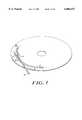
- FIG. 1is a simplified view of a thin-film magnetic recording head according to the invention disposed above a data track of a magnetic medium;
- FIG. 2is a cross sectional view, along section 2--2 of FIG. 1, showing one embodiment of the thin-film magnetic recording head, disposed above a data track of a magnetic medium;
- FIGS. 3(a) and 3(b)are perspective views from above a lithographically fabricated multi-layer device, which contains part of the recording head of FIG. 1, at the completion of a first and second step in the fabrication process, respectively;
- FIGS. 4(a)-4(e)are cross sectional views of the multi-layer device of FIGS. 3(a) and 3(b) at various stages in one embodiment of the fabrication process;
- FIG. 5is a perspective view from above the multi-layer device of FIG. 3(b) after cleaving the device to expose the read and write heads and their associated marker elements;
- FIG. 6shows the cleaved, multi-layer device of FIG. 5 containing a defective write head, seen from the plane of the cleaved surface;
- FIG. 7is a schematic view of one system for manufacturing the thin-film recording head of FIG. 1 according to the invention.
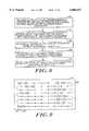
- FIG. 8is a flow chart illustrating one process according to the invention for manufacturing the thin-film recording head of FIG. 1;
- FIG. 9illustrates schematically the sequence of a raster scan of a focused particle beam within the trim outlines of FIG. 6;
- FIG. 10(a)shows one embodiment of the recording head of FIG. 1 with desired pole-tip configuration as seen from the plane of the cleaved surface;
- FIG. 1illustrates an example of one type of thin-film recording head.
- FIG. 1depicts a hard computer-memory disk 15, a recording head 13, a pole-tip assembly 14, a data track 16, and an extension arm 18.
- the illustrated recording head 13is disposed at the distal end of the arm 18 and is located just above the rotating disk 15.
- the recording headrecords and reads digital data by generating or detecting magnetization states that form the data track 16 on the disk 15.
- a write headtypically includes at least three parts: the core, the coil and the gap.
- the coreincludes poles 21b and 24b.
- the coil 23, shown in cross section,is wrapped around the core.
- the write gap 26separates the pole-tips 21 and 24 of the pole-tip assembly.
- the core structureis usually called the yoke.
- Thin-film headscan be made of thin layers of permalloy (81Ni/19Fe) or AlFeSil (an aluminum, iron and silicon alloy) in, typically, two to four ⁇ m thicknesses.
- the coilcan be made of copper and the gap can be made of Al 2 O 3 .
- FIGS. 3(a) and 3(b)are perspective views from above of one embodiment of a lithographically fabricated multi-layer device, which manufacturers can use to produce the recording head of FIG. 1.
- FIGS. 3(a) and 3(b)show the multi-layer device at the completion of a first and second step in the fabrication process, respectively.
- FIG. 3(a)shows the multi-layer device after completion of a first patterning step and before completion of a second patterning step.
- a first structural element 11 and a first marker element 12are present in the multi-layer device.
- element 12need not be a square.
- the marker element 12has a similar configuration to the structural element 11.
- FIG. 3(b)shows the multilayer device after completion of the second patterning step.
- Photoresistis a polymeric mixture that is deposited as a thin layer, perhaps one ⁇ m thick, upon the multi-layer device. Irradiation with light in the near ultraviolet region of the spectrum modifies the chemical properties of the photoresist, and in "positive" photoresist, makes it more soluble to certain developers. Thus, one step frequently employed in microstructure fabrication is the projection of the image of a mask onto the photoresist layer. It becomes possible to remove the exposed region of the photoresist by dissolving it with a suitable developer.
- the inventionis understood as a lithographic process including the steps of 1) patterning in a first common lithographic layer 1a, a first structural element 11 (e.g. a read head) and, at a known distance and direction, a first marker element 11a; and 2) patterning in a second common lithographic layer 21a, a second structural element 21 (e.g. a write head) and a second marker element 22.
- the above patterning stepsprovide the structural and marker elements so that they intersect a single geometrical surface 32 that extends transversely to the first and second lithographic layers.
- the geometrical surfaceis planar.
- the ion column 72includes an ion source 74, an extraction electrode 76, a focusing element 78, deflection elements 79, and a focused ion beam 80.
- the ion column 72sits above the vacuum chamber 82, and the vacuum chamber 82 houses a stage 84, a platform 86, a read/write head 90, a secondary particle detector 88 and a charge neutralization element 92.
- the optional reactant material delivery system 94includes a reservoir 96, a manometer 100, a motorized valve element 102, and delivery conduit 104.
- the user control station 110can include a processor 112, a pattern recognition element 114, a memory element 116, a display element 120, a scan generator element 122, and dwell registers 124.
- a Z axis, that is generally understood as extending parallel to the path of the focused ion beam 80is also generally orthogonal to the plane defined by the X and Y axis of the surface of the recording head 90.
- FIG. 10(c)shows the first two steps in a four step process for fabricating the thin-film recording head of FIG. 2 using the multi-layer device of FIG. 10(b).
- the focused ion beam system 70locates the top edge of layer 24a.
- the system 70locates the top edge of layer 24a by imaging a vertical section 99 of the multi-layer device avoiding the structural and marker elements. For example, the system can image a vertical section on the far left side 99 of the multi-layer device.
- the systemobtains a vertical reference point.
- the vertical axisis the Y axis.
Landscapes
- Engineering & Computer Science (AREA)
- Manufacturing & Machinery (AREA)
- Physics & Mathematics (AREA)
- Plasma & Fusion (AREA)
- Chemical & Material Sciences (AREA)
- Analytical Chemistry (AREA)
- Magnetic Heads (AREA)
Abstract
Description
Claims (4)
Priority Applications (6)
| Application Number | Priority Date | Filing Date | Title |
|---|---|---|---|
| US08/810,837US6004437A (en) | 1996-04-19 | 1997-03-04 | Thin-film magnetic recording head manufacturing method |
| AU66752/98AAU6675298A (en) | 1997-03-04 | 1998-03-02 | Thin-film magnetic recording head manufacture |
| PCT/US1998/003964WO1998039770A1 (en) | 1997-03-04 | 1998-03-02 | Thin-film magnetic recording head manufacture |
| US09/370,753US6354438B1 (en) | 1996-04-19 | 1999-08-09 | Focused ion beam apparatus for forming thin-film magnetic recording heads |
| US10/085,490US6579665B2 (en) | 1996-04-19 | 2002-02-28 | Thin-film magnetic recording head manufacture |
| US10/462,389US7045275B2 (en) | 1996-04-19 | 2003-06-16 | Thin-film magnetic recording head manufacture |
Applications Claiming Priority (2)
| Application Number | Priority Date | Filing Date | Title |
|---|---|---|---|
| US08/635,063US5916424A (en) | 1996-04-19 | 1996-04-19 | Thin film magnetic recording heads and systems and methods for manufacturing the same |
| US08/810,837US6004437A (en) | 1996-04-19 | 1997-03-04 | Thin-film magnetic recording head manufacturing method |
Related Parent Applications (2)
| Application Number | Title | Priority Date | Filing Date |
|---|---|---|---|
| US08/635,063Continuation-In-PartUS5916424A (en) | 1996-04-19 | 1996-04-19 | Thin film magnetic recording heads and systems and methods for manufacturing the same |
| US08/635,063ContinuationUS5916424A (en) | 1996-04-19 | 1996-04-19 | Thin film magnetic recording heads and systems and methods for manufacturing the same |
Related Child Applications (1)
| Application Number | Title | Priority Date | Filing Date |
|---|---|---|---|
| US09/370,753ContinuationUS6354438B1 (en) | 1996-04-19 | 1999-08-09 | Focused ion beam apparatus for forming thin-film magnetic recording heads |
Publications (1)
| Publication Number | Publication Date |
|---|---|
| US6004437Atrue US6004437A (en) | 1999-12-21 |
Family
ID=24546287
Family Applications (5)
| Application Number | Title | Priority Date | Filing Date |
|---|---|---|---|
| US08/635,063Expired - LifetimeUS5916424A (en) | 1996-04-19 | 1996-04-19 | Thin film magnetic recording heads and systems and methods for manufacturing the same |
| US08/810,837Expired - LifetimeUS6004437A (en) | 1996-04-19 | 1997-03-04 | Thin-film magnetic recording head manufacturing method |
| US09/370,753Expired - LifetimeUS6354438B1 (en) | 1996-04-19 | 1999-08-09 | Focused ion beam apparatus for forming thin-film magnetic recording heads |
| US10/085,490Expired - LifetimeUS6579665B2 (en) | 1996-04-19 | 2002-02-28 | Thin-film magnetic recording head manufacture |
| US10/462,389Expired - Fee RelatedUS7045275B2 (en) | 1996-04-19 | 2003-06-16 | Thin-film magnetic recording head manufacture |
Family Applications Before (1)
| Application Number | Title | Priority Date | Filing Date |
|---|---|---|---|
| US08/635,063Expired - LifetimeUS5916424A (en) | 1996-04-19 | 1996-04-19 | Thin film magnetic recording heads and systems and methods for manufacturing the same |
Family Applications After (3)
| Application Number | Title | Priority Date | Filing Date |
|---|---|---|---|
| US09/370,753Expired - LifetimeUS6354438B1 (en) | 1996-04-19 | 1999-08-09 | Focused ion beam apparatus for forming thin-film magnetic recording heads |
| US10/085,490Expired - LifetimeUS6579665B2 (en) | 1996-04-19 | 2002-02-28 | Thin-film magnetic recording head manufacture |
| US10/462,389Expired - Fee RelatedUS7045275B2 (en) | 1996-04-19 | 2003-06-16 | Thin-film magnetic recording head manufacture |
Country Status (6)
| Country | Link |
|---|---|
| US (5) | US5916424A (en) |
| EP (1) | EP0894320B1 (en) |
| JP (1) | JP4236058B2 (en) |
| CA (1) | CA2252979A1 (en) |
| DE (1) | DE69723069T2 (en) |
| WO (1) | WO1997040493A1 (en) |
Cited By (6)
| Publication number | Priority date | Publication date | Assignee | Title |
|---|---|---|---|---|
| US6238582B1 (en)* | 1999-03-30 | 2001-05-29 | Veeco Instruments, Inc. | Reactive ion beam etching method and a thin film head fabricated using the method |
| US6354438B1 (en)* | 1996-04-19 | 2002-03-12 | Micrion Corporation | Focused ion beam apparatus for forming thin-film magnetic recording heads |
| US20030228542A1 (en)* | 2002-06-06 | 2003-12-11 | Seagate Technology Llc | Method and structure to reduce e-beam and magnetic material interactions |
| US6824644B2 (en)* | 1997-06-13 | 2004-11-30 | Fei Company | Thin-film magnetic recording head manufacture using selective imaging |
| US20040264046A1 (en)* | 2003-06-25 | 2004-12-30 | Hitachi Global Storage Technologies | Magnetic head with thinned T-shaped write pole and its fabrication |
| US6987067B2 (en) | 2002-08-21 | 2006-01-17 | International Business Machines Corporation | Semiconductor copper line cutting method |
Families Citing this family (65)
| Publication number | Priority date | Publication date | Assignee | Title |
|---|---|---|---|---|
| AU6675298A (en)* | 1997-03-04 | 1998-09-22 | Micrion Corporation | Thin-film magnetic recording head manufacture |
| JPH117608A (en)* | 1997-04-25 | 1999-01-12 | Fujitsu Ltd | Magnetic head and method of manufacturing the same |
| FR2764110B1 (en)* | 1997-05-28 | 1999-08-20 | Univ Paris Curie | DEVICE AND METHOD FOR ION ETCHING |
| US6459949B1 (en)* | 1998-10-21 | 2002-10-01 | Advanced Micro Devices, Inc. | System and method for corrective action tracking in semiconductor processing |
| US7773340B2 (en) | 1999-02-23 | 2010-08-10 | Advanced Research Corporation | Patterned magnetic recording head having a gap pattern with substantially elliptical or substantially diamond-shaped termination pattern |
| US7196870B2 (en) | 1999-02-23 | 2007-03-27 | Advanced Research Corporation | Patterned magnetic recording head with termination pattern having a curved portion |
| US20030093894A1 (en) | 1999-02-23 | 2003-05-22 | Dugas Matthew P. | Double layer patterning and technique for making a magnetic recording head |
| US6269533B2 (en) | 1999-02-23 | 2001-08-07 | Advanced Research Corporation | Method of making a patterned magnetic recording head |
| US6331711B1 (en)* | 1999-08-06 | 2001-12-18 | Etec Systems, Inc. | Correction for systematic, low spatial frequency critical dimension variations in lithography |
| WO2001054163A1 (en)* | 2000-01-21 | 2001-07-26 | Koninklijke Philips Electronics N.V. | Shaped and low density focused ion beams |
| US6419566B1 (en) | 2000-02-11 | 2002-07-16 | International Business Machines Corporation | System for cleaning contamination from magnetic recording media rows |
| US6977386B2 (en)* | 2001-01-19 | 2005-12-20 | Fei Company | Angular aperture shaped beam system and method |
| FR2823005B1 (en)* | 2001-03-28 | 2003-05-16 | Centre Nat Rech Scient | DEVICE FOR GENERATING AN ION BEAM AND METHOD OF ADJUSTING THE BEAM |
| JP2003151479A (en)* | 2001-11-15 | 2003-05-23 | Hitachi Ltd | Charge neutralization control method and charged particle beam apparatus using the same |
| US20030127424A1 (en)* | 2002-01-08 | 2003-07-10 | Seagate Technology Llc | Method of fabricating magnetic recording heads using asymmetric focused-Ion-beam trimming |
| US6996033B2 (en) | 2002-06-19 | 2006-02-07 | Advanced Research Corporation | Optical path for a thermal-assisted magnetic recording head |
| US20040045671A1 (en)* | 2002-09-10 | 2004-03-11 | Ed Rejda | Selective etching device |
| US7008803B2 (en)* | 2002-10-24 | 2006-03-07 | International Business Machines Corporation | Method of reworking structures incorporating low-k dielectric materials |
| US6979389B2 (en)* | 2003-06-30 | 2005-12-27 | Seagate Technology Llc | Micro-actuation apparatus for head ABS planarity (PTR) control during slider machining |
| US7511280B2 (en)* | 2003-10-16 | 2009-03-31 | Alis Corporation | Ion sources, systems and methods |
| US7557360B2 (en)* | 2003-10-16 | 2009-07-07 | Alis Corporation | Ion sources, systems and methods |
| US7554097B2 (en)* | 2003-10-16 | 2009-06-30 | Alis Corporation | Ion sources, systems and methods |
| US7786451B2 (en)* | 2003-10-16 | 2010-08-31 | Alis Corporation | Ion sources, systems and methods |
| US8110814B2 (en) | 2003-10-16 | 2012-02-07 | Alis Corporation | Ion sources, systems and methods |
| US7557359B2 (en)* | 2003-10-16 | 2009-07-07 | Alis Corporation | Ion sources, systems and methods |
| US7521693B2 (en)* | 2003-10-16 | 2009-04-21 | Alis Corporation | Ion sources, systems and methods |
| US7554096B2 (en)* | 2003-10-16 | 2009-06-30 | Alis Corporation | Ion sources, systems and methods |
| US7786452B2 (en)* | 2003-10-16 | 2010-08-31 | Alis Corporation | Ion sources, systems and methods |
| US7495232B2 (en)* | 2003-10-16 | 2009-02-24 | Alis Corporation | Ion sources, systems and methods |
| US7485873B2 (en)* | 2003-10-16 | 2009-02-03 | Alis Corporation | Ion sources, systems and methods |
| US7511279B2 (en)* | 2003-10-16 | 2009-03-31 | Alis Corporation | Ion sources, systems and methods |
| US7557358B2 (en) | 2003-10-16 | 2009-07-07 | Alis Corporation | Ion sources, systems and methods |
| US7414243B2 (en)* | 2005-06-07 | 2008-08-19 | Alis Corporation | Transmission ion microscope |
| US7601953B2 (en)* | 2006-03-20 | 2009-10-13 | Alis Corporation | Systems and methods for a gas field ion microscope |
| US7321118B2 (en)* | 2005-06-07 | 2008-01-22 | Alis Corporation | Scanning transmission ion microscope |
| US7504639B2 (en)* | 2003-10-16 | 2009-03-17 | Alis Corporation | Ion sources, systems and methods |
| US7368727B2 (en)* | 2003-10-16 | 2008-05-06 | Alis Technology Corporation | Atomic level ion source and method of manufacture and operation |
| US7518122B2 (en) | 2003-10-16 | 2009-04-14 | Alis Corporation | Ion sources, systems and methods |
| US7557361B2 (en)* | 2003-10-16 | 2009-07-07 | Alis Corporation | Ion sources, systems and methods |
| US9159527B2 (en)* | 2003-10-16 | 2015-10-13 | Carl Zeiss Microscopy, Llc | Systems and methods for a gas field ionization source |
| US7488952B2 (en)* | 2003-10-16 | 2009-02-10 | Alis Corporation | Ion sources, systems and methods |
| US7611610B2 (en) | 2003-11-18 | 2009-11-03 | Fei Company | Method and apparatus for controlling topographical variation on a milled cross-section of a structure |
| US7015146B2 (en)* | 2004-01-06 | 2006-03-21 | International Business Machines Corporation | Method of processing backside unlayering of MOSFET devices for electrical and physical characterization including a collimated ion plasma |
| US7129484B2 (en)* | 2004-01-21 | 2006-10-31 | Hitachi Global Storage Technologies Netherlands B.V. | Method for pattern recognition in energized charge particle beam wafer/slider inspection/measurement systems in presence of electrical charge |
| US7086139B2 (en)* | 2004-04-30 | 2006-08-08 | Hitachi Global Storage Technologies Netherlands B.V. | Methods of making magnetic write heads using electron beam lithography |
| JP4486462B2 (en)* | 2004-09-29 | 2010-06-23 | 日本電子株式会社 | Sample preparation method and sample preparation apparatus |
| WO2006098828A2 (en)* | 2005-03-10 | 2006-09-21 | Matsushita Electric Industrial Co., Ltd. | Structured diamond tool made by focused ion beam nanomachining |
| EP1722398B1 (en)* | 2005-05-14 | 2009-11-25 | FEI Company | Deflection Signal Compensation for Charged Particle Beam |
| US20070116373A1 (en)* | 2005-11-23 | 2007-05-24 | Sonosite, Inc. | Multi-resolution adaptive filtering |
| WO2007067296A2 (en)* | 2005-12-02 | 2007-06-14 | Alis Corporation | Ion sources, systems and methods |
| JP5600371B2 (en)* | 2006-02-15 | 2014-10-01 | エフ・イ−・アイ・カンパニー | Sputtering coating of protective layer for charged particle beam processing |
| TW200737267A (en)* | 2006-03-20 | 2007-10-01 | Alis Corp | Systems and methods for a helium ion pump |
| US8357913B2 (en) | 2006-10-20 | 2013-01-22 | Fei Company | Method and apparatus for sample extraction and handling |
| US8134124B2 (en) | 2006-10-20 | 2012-03-13 | Fei Company | Method for creating S/tem sample and sample structure |
| US7804068B2 (en)* | 2006-11-15 | 2010-09-28 | Alis Corporation | Determining dopant information |
| US7880151B2 (en) | 2008-02-28 | 2011-02-01 | Fei Company | Beam positioning for beam processing |
| WO2010132221A2 (en)* | 2009-05-12 | 2010-11-18 | Carl Zeiss Nts, Llc. | Gas field ion microscopes having multiple operation modes |
| JP2010277624A (en)* | 2009-05-26 | 2010-12-09 | Toshiba Storage Device Corp | Magnetic recording device, head evaluation device, spin stand device, and write pole erasure evaluation method |
| NL2004888A (en)* | 2009-06-29 | 2010-12-30 | Asml Netherlands Bv | Deposition method and apparatus. |
| WO2011025998A2 (en) | 2009-08-28 | 2011-03-03 | Fei Company | Pattern modification schemes for improved fib patterning |
| US8350237B2 (en)* | 2010-03-31 | 2013-01-08 | Fei Company | Automated slice milling for viewing a feature |
| EP3528276A3 (en) | 2011-05-13 | 2019-09-04 | Fibics Incorporated | Microscopy imaging method |
| EP2610889A3 (en) | 2011-12-27 | 2015-05-06 | Fei Company | Drift control in a charged particle beam system |
| CN111508535B (en) | 2020-03-13 | 2021-08-13 | 华为技术有限公司 | A data writing and reading method, device and system |
| US20250112024A1 (en)* | 2023-09-28 | 2025-04-03 | Fei Company | Adaptive slice depth in slice & view workflow |
Citations (20)
| Publication number | Priority date | Publication date | Assignee | Title |
|---|---|---|---|---|
| US4457803A (en)* | 1981-12-18 | 1984-07-03 | Tokyo Shibaura Denki Kabushiki Kaisha | Processing method using a focused ion beam |
| JPS6010407A (en)* | 1983-06-29 | 1985-01-19 | Hitachi Ltd | Production of magnetic head |
| GB2166888A (en)* | 1984-11-13 | 1986-05-14 | Magnetic Peripherals Inc | Process for producing negative pressure slider using a photoresist |
| US4639301A (en)* | 1985-04-24 | 1987-01-27 | Micrion Limited Partnership | Focused ion beam processing |
| US4874947A (en)* | 1988-02-26 | 1989-10-17 | Micrion Corporation | Focused ion beam imaging and process control |
| GB2227601A (en)* | 1988-12-01 | 1990-08-01 | Seiko Instr Inc | "Preparing a micro-section in a sample for observation" |
| EP0452846A2 (en)* | 1990-04-16 | 1991-10-23 | Hitachi, Ltd. | Narrow track thin film magnetic head and fabrication method thereof |
| US5079662A (en)* | 1988-09-30 | 1992-01-07 | Hitachi, Ltd. | Compound magnetic head having a recording head and a reproducing magnetoresitive head integrated therein |
| JPH0444610A (en)* | 1990-06-12 | 1992-02-14 | Hitachi Ltd | Composite thin film magnetic head and its manufacturing method |
| JPH04205705A (en)* | 1990-11-29 | 1992-07-27 | Hitachi Ltd | Thin film magnetic head and magnetic disk device |
| JPH05143939A (en)* | 1991-11-20 | 1993-06-11 | Nec Corp | Composite type thin-film magnetic head and production thereof |
| JPH05143938A (en)* | 1991-11-22 | 1993-06-11 | Sony Corp | Magneto-resistance effect type magnetic head |
| US5314596A (en)* | 1990-06-29 | 1994-05-24 | Digital Equipment Corporation | Process for fabricating magnetic film recording head for use with a magnetic recording media |
| JPH06338033A (en)* | 1993-05-26 | 1994-12-06 | Sanyo Electric Co Ltd | Composite thin film magnetic head |
| JPH06349026A (en)* | 1993-06-08 | 1994-12-22 | Hitachi Metals Ltd | Thin-film magnetic head |
| US5401972A (en)* | 1993-09-02 | 1995-03-28 | Schlumberger Technologies, Inc. | Layout overlay for FIB operations |
| US5404635A (en)* | 1992-05-21 | 1995-04-11 | Das Devices, Inc. | Method of making a narrow track thin film head |
| US5452166A (en)* | 1993-10-01 | 1995-09-19 | Applied Magnetics Corporation | Thin film magnetic recording head for minimizing undershoots and a method for manufacturing the same |
| US5495378A (en)* | 1995-01-30 | 1996-02-27 | Seagate Technology, Inc. | Magnetoresistive sensor with improved performance and processability |
| WO1997040493A1 (en)* | 1996-04-19 | 1997-10-30 | Micrion Corporation | Thin-film magnetic recording heads and systems and methods for manufacturing the same |
Family Cites Families (18)
| Publication number | Priority date | Publication date | Assignee | Title |
|---|---|---|---|---|
| US4078300A (en)* | 1975-01-10 | 1978-03-14 | Compagnie Internationale Pour L'informatique | Method of making an integrated magnetic head having pole-pieces of a reduced frontal width |
| JPH0616391B2 (en)* | 1984-07-13 | 1994-03-02 | 株式会社日立製作所 | Ion beam irradiation device |
| JPS61175914A (en)* | 1985-01-30 | 1986-08-07 | Nec Kansai Ltd | Working method of magnetic head core |
| JPS61237216A (en)* | 1985-04-12 | 1986-10-22 | Fujitsu Ltd | Manufacturing method of thin film magnetic head |
| JP2713923B2 (en)* | 1987-10-07 | 1998-02-16 | 株式会社日立製作所 | Device processing method using focused ion beam |
| DE3818393A1 (en)* | 1988-05-30 | 1989-12-14 | Siemens Ag | THIN FILM MAGNET HEAD WITH HIGH SUB-TRACK DAMPING |
| SE8904179L (en) | 1988-12-29 | 1990-06-30 | Colgate Palmolive Co | PRE-PACKED ORAL ANTI-PLAQUE COMPOSITIONS |
| JP3639603B2 (en)* | 1991-06-03 | 2005-04-20 | 株式会社日立製作所 | Magnetic disk unit |
| US5149976A (en)* | 1990-08-31 | 1992-09-22 | Hughes Aircraft Company | Charged particle beam pattern generation apparatus and method |
| JP3005969B2 (en)* | 1990-10-05 | 2000-02-07 | ティーディーケイ株式会社 | Magnetic head |
| US5217819A (en)* | 1991-05-08 | 1993-06-08 | U.S. Philips Corporation | Method of manufacturing a thin-film magnetic head and magnetic head |
| JPH05101352A (en)* | 1991-10-02 | 1993-04-23 | Matsushita Electric Ind Co Ltd | Method for polishing magnetic head and method for adjusting height of magnetic head |
| JPH05298612A (en)* | 1992-04-13 | 1993-11-12 | Nec Corp | Magnetic head and its manufacture |
| JPH06103512A (en)* | 1992-09-18 | 1994-04-15 | Sony Corp | Method and device matching magnetic head block |
| JPH06243430A (en)* | 1993-02-22 | 1994-09-02 | General Signal Japan Kk | Exposure method and device for bar substrate for thin-film magnetic head |
| JP3117836B2 (en)* | 1993-03-02 | 2000-12-18 | セイコーインスツルメンツ株式会社 | Focused ion beam equipment |
| DE4421517A1 (en)* | 1993-06-28 | 1995-01-05 | Schlumberger Technologies Inc | Method for removing or depositing material by means of a particle beam and device for carrying out the method |
| US5630949A (en)* | 1995-06-01 | 1997-05-20 | Tfr Technologies, Inc. | Method and apparatus for fabricating a piezoelectric resonator to a resonant frequency |
- 1996
- 1996-04-19USUS08/635,063patent/US5916424A/ennot_activeExpired - Lifetime
- 1997
- 1997-03-04USUS08/810,837patent/US6004437A/ennot_activeExpired - Lifetime
- 1997-04-16JPJP53814197Apatent/JP4236058B2/ennot_activeExpired - Fee Related
- 1997-04-16EPEP97918610Apatent/EP0894320B1/ennot_activeExpired - Lifetime
- 1997-04-16CACA002252979Apatent/CA2252979A1/ennot_activeAbandoned
- 1997-04-16WOPCT/US1997/006158patent/WO1997040493A1/enactiveIP Right Grant
- 1997-04-16DEDE69723069Tpatent/DE69723069T2/ennot_activeExpired - Lifetime
- 1999
- 1999-08-09USUS09/370,753patent/US6354438B1/ennot_activeExpired - Lifetime
- 2002
- 2002-02-28USUS10/085,490patent/US6579665B2/ennot_activeExpired - Lifetime
- 2003
- 2003-06-16USUS10/462,389patent/US7045275B2/ennot_activeExpired - Fee Related
Patent Citations (22)
| Publication number | Priority date | Publication date | Assignee | Title |
|---|---|---|---|---|
| US4457803A (en)* | 1981-12-18 | 1984-07-03 | Tokyo Shibaura Denki Kabushiki Kaisha | Processing method using a focused ion beam |
| JPS6010407A (en)* | 1983-06-29 | 1985-01-19 | Hitachi Ltd | Production of magnetic head |
| GB2166888A (en)* | 1984-11-13 | 1986-05-14 | Magnetic Peripherals Inc | Process for producing negative pressure slider using a photoresist |
| US4639301A (en)* | 1985-04-24 | 1987-01-27 | Micrion Limited Partnership | Focused ion beam processing |
| US4639301B1 (en)* | 1985-04-24 | 1989-06-27 | Micrion Limited Partnership | Focused ion beam processing |
| US4639301B2 (en)* | 1985-04-24 | 1999-05-04 | Micrion Corp | Focused ion beam processing |
| US4874947A (en)* | 1988-02-26 | 1989-10-17 | Micrion Corporation | Focused ion beam imaging and process control |
| US5079662A (en)* | 1988-09-30 | 1992-01-07 | Hitachi, Ltd. | Compound magnetic head having a recording head and a reproducing magnetoresitive head integrated therein |
| GB2227601A (en)* | 1988-12-01 | 1990-08-01 | Seiko Instr Inc | "Preparing a micro-section in a sample for observation" |
| EP0452846A2 (en)* | 1990-04-16 | 1991-10-23 | Hitachi, Ltd. | Narrow track thin film magnetic head and fabrication method thereof |
| JPH0444610A (en)* | 1990-06-12 | 1992-02-14 | Hitachi Ltd | Composite thin film magnetic head and its manufacturing method |
| US5314596A (en)* | 1990-06-29 | 1994-05-24 | Digital Equipment Corporation | Process for fabricating magnetic film recording head for use with a magnetic recording media |
| JPH04205705A (en)* | 1990-11-29 | 1992-07-27 | Hitachi Ltd | Thin film magnetic head and magnetic disk device |
| JPH05143939A (en)* | 1991-11-20 | 1993-06-11 | Nec Corp | Composite type thin-film magnetic head and production thereof |
| JPH05143938A (en)* | 1991-11-22 | 1993-06-11 | Sony Corp | Magneto-resistance effect type magnetic head |
| US5404635A (en)* | 1992-05-21 | 1995-04-11 | Das Devices, Inc. | Method of making a narrow track thin film head |
| JPH06338033A (en)* | 1993-05-26 | 1994-12-06 | Sanyo Electric Co Ltd | Composite thin film magnetic head |
| JPH06349026A (en)* | 1993-06-08 | 1994-12-22 | Hitachi Metals Ltd | Thin-film magnetic head |
| US5401972A (en)* | 1993-09-02 | 1995-03-28 | Schlumberger Technologies, Inc. | Layout overlay for FIB operations |
| US5452166A (en)* | 1993-10-01 | 1995-09-19 | Applied Magnetics Corporation | Thin film magnetic recording head for minimizing undershoots and a method for manufacturing the same |
| US5495378A (en)* | 1995-01-30 | 1996-02-27 | Seagate Technology, Inc. | Magnetoresistive sensor with improved performance and processability |
| WO1997040493A1 (en)* | 1996-04-19 | 1997-10-30 | Micrion Corporation | Thin-film magnetic recording heads and systems and methods for manufacturing the same |
Non-Patent Citations (4)
| Title |
|---|
| Futamoto, Masaaki et al., "Development of Technologies for 2-Gb/in2 Areal Density Recording", Electronics and Communications in Japan, Part II-Electronics, vol. 76, No. 3 (Mar. 1993) pp. 94-103. |
| Futamoto, Masaaki et al., Development of Technologies for 2 Gb/in2 Areal Density Recording , Electronics and Communications in Japan, Part II Electronics , vol. 76, No. 3 (Mar. 1993) pp. 94 103.* |
| Mallinson, John C., Magneto Resistive Heads, Fundamentals and Applications , (Academic Press, Inc., San Diego 1996) Chapter 8, pp. 66 78 and Chapter 14, pp. 110 119.* |
| Mallinson, John C., Magneto-Resistive Heads, Fundamentals and Applications, (Academic Press, Inc., San Diego 1996) Chapter 8, pp. 66-78 and Chapter 14, pp. 110-119. |
Cited By (13)
| Publication number | Priority date | Publication date | Assignee | Title |
|---|---|---|---|---|
| US6354438B1 (en)* | 1996-04-19 | 2002-03-12 | Micrion Corporation | Focused ion beam apparatus for forming thin-film magnetic recording heads |
| US6579665B2 (en)* | 1996-04-19 | 2003-06-17 | Fei Company | Thin-film magnetic recording head manufacture |
| US20040253543A1 (en)* | 1996-04-19 | 2004-12-16 | Lee Randall Grafton | Thin-film magnetic recording head manufacture |
| US7045275B2 (en)* | 1996-04-19 | 2006-05-16 | Fei Company | Thin-film magnetic recording head manufacture |
| US20050139320A1 (en)* | 1997-06-13 | 2005-06-30 | Fei Company | Thin-film magnetic recording head manufacture using selective imaging |
| US7378003B2 (en) | 1997-06-13 | 2008-05-27 | Fei Company | Thin-film magnetic recording head manufacture using selective imaging |
| US6824644B2 (en)* | 1997-06-13 | 2004-11-30 | Fei Company | Thin-film magnetic recording head manufacture using selective imaging |
| US6238582B1 (en)* | 1999-03-30 | 2001-05-29 | Veeco Instruments, Inc. | Reactive ion beam etching method and a thin film head fabricated using the method |
| US20030228542A1 (en)* | 2002-06-06 | 2003-12-11 | Seagate Technology Llc | Method and structure to reduce e-beam and magnetic material interactions |
| WO2003105129A1 (en)* | 2002-06-06 | 2003-12-18 | Seagate Technology Llc | Method and structure to reduce e-beam and magnetic material interactions |
| US6987067B2 (en) | 2002-08-21 | 2006-01-17 | International Business Machines Corporation | Semiconductor copper line cutting method |
| US20040264046A1 (en)* | 2003-06-25 | 2004-12-30 | Hitachi Global Storage Technologies | Magnetic head with thinned T-shaped write pole and its fabrication |
| US7092206B2 (en) | 2003-06-25 | 2006-08-15 | Hitachi Global Storage Technologies Netherlands B.V. | Magnetic head with magnetic layers of differing widths and third pole with reduced thickness |
Also Published As
| Publication number | Publication date |
|---|---|
| US20020144892A1 (en) | 2002-10-10 |
| US20040253543A1 (en) | 2004-12-16 |
| US6579665B2 (en) | 2003-06-17 |
| DE69723069T2 (en) | 2004-04-29 |
| US6354438B1 (en) | 2002-03-12 |
| JP2000509181A (en) | 2000-07-18 |
| JP4236058B2 (en) | 2009-03-11 |
| CA2252979A1 (en) | 1997-10-30 |
| EP0894320A1 (en) | 1999-02-03 |
| DE69723069D1 (en) | 2003-07-31 |
| EP0894320B1 (en) | 2003-06-25 |
| US7045275B2 (en) | 2006-05-16 |
| US5916424A (en) | 1999-06-29 |
| WO1997040493A1 (en) | 1997-10-30 |
Similar Documents
| Publication | Publication Date | Title |
|---|---|---|
| US6004437A (en) | Thin-film magnetic recording head manufacturing method | |
| US8163145B2 (en) | Method and apparatus for controlling topographical variation on a milled cross-section of a structure | |
| US6104576A (en) | Inductive head with reduced height insulation stack due to partial coverage zero throat height defining insulation layer | |
| US5752309A (en) | Method and apparatus for precisely dimensioning pole tips of a magnetic transducing head structure | |
| US6332962B1 (en) | Thin-film magnetic recording head manufacture using selective imaging | |
| JP2961452B2 (en) | Information processing device | |
| JP2004206862A (en) | Double layer patterning method and pattern milling method | |
| JP2000040208A (en) | Thin-film magnetic head and magnetic disk drive equipped with the same | |
| JP2000207738A (en) | Manufacturing method of information carrier | |
| US5910871A (en) | Magnetic head having track width specified by grooves formed with projection ion beam | |
| WO1998039770A1 (en) | Thin-film magnetic recording head manufacture | |
| US6539610B1 (en) | Method for manufacturing a magnetic write head | |
| KR19990036438A (en) | Method and apparatus for precise dimension determination of pole tip of magnetic conversion head structure | |
| US7480983B2 (en) | Method for making magnetic write head | |
| US7527917B2 (en) | Exposure method and exposure apparatus | |
| US20030228542A1 (en) | Method and structure to reduce e-beam and magnetic material interactions | |
| JPH11219680A (en) | Focused ion beam processing method | |
| JP2000222725A5 (en) | ||
| JP2000222725A (en) | Pattern formation to disk-like recording medium, pattern forming device and disk-like recording medium | |
| JP2001256609A (en) | Method for manufacturing thin-film magnetic head |
Legal Events
| Date | Code | Title | Description |
|---|---|---|---|
| AS | Assignment | Owner name:MICRION CORPORATION, MASSACHUSETTS Free format text:ASSIGNMENT OF ASSIGNORS INTEREST;ASSIGNORS:LEE, RANDALL GRAFTON;LIBBY, CHARLES J.;REEL/FRAME:008556/0007 Effective date:19970527 | |
| AS | Assignment | Owner name:FLEET NATIONAL BANK, MASSACHUSETTS Free format text:SECURITY INTEREST;ASSIGNOR:MICRION CORPORATION;REEL/FRAME:008709/0125 Effective date:19970731 | |
| STCF | Information on status: patent grant | Free format text:PATENTED CASE | |
| AS | Assignment | Owner name:FEI COMPANY, OREGON Free format text:MERGER;ASSIGNOR:MICRION CORPORATION;REEL/FRAME:012906/0394 Effective date:20011231 Owner name:MICRION CORPORATION, ONTARIO Free format text:CHANGE OF NAME;ASSIGNOR:M.C. ACQUISITION CORPORATION;REEL/FRAME:012906/0404 Effective date:19990805 Owner name:M.C. ACQUISITION CORPORATION, OREGON Free format text:MERGER;ASSIGNOR:MICRION CORPORATION;REEL/FRAME:012906/0422 Effective date:19990813 | |
| FEPP | Fee payment procedure | Free format text:PAT HOLDER NO LONGER CLAIMS SMALL ENTITY STATUS, ENTITY STATUS SET TO UNDISCOUNTED (ORIGINAL EVENT CODE: STOL); ENTITY STATUS OF PATENT OWNER: LARGE ENTITY | |
| FEPP | Fee payment procedure | Free format text:PAYOR NUMBER ASSIGNED (ORIGINAL EVENT CODE: ASPN); ENTITY STATUS OF PATENT OWNER: LARGE ENTITY Free format text:PAYER NUMBER DE-ASSIGNED (ORIGINAL EVENT CODE: RMPN); ENTITY STATUS OF PATENT OWNER: LARGE ENTITY | |
| FPAY | Fee payment | Year of fee payment:4 | |
| REMI | Maintenance fee reminder mailed | ||
| FPAY | Fee payment | Year of fee payment:8 | |
| AS | Assignment | Owner name:J.P. MORGAN EUROPE LIMITED, AS ALTERNATIVE CURRENC Free format text:SECURITY AGREEMENT;ASSIGNOR:FEI COMPANY;REEL/FRAME:021064/0319 Effective date:20080604 Owner name:JP MORGAN CHASE BANK, N.A. (AS ADMINISTRATIVE AGEN Free format text:SECURITY AGREEMENT;ASSIGNOR:FEI COMPANY;REEL/FRAME:021064/0319 Effective date:20080604 | |
| FPAY | Fee payment | Year of fee payment:12 | |
| AS | Assignment | Owner name:FEI COMPANY, OREGON Free format text:RELEASE BY SECURED PARTY;ASSIGNORS:JPMORGAN CHASE BANK, N.A.;J.P. MORGAN EUROPE LIMITED;REEL/FRAME:038328/0787 Effective date:20160324 |