US6002614A - Memory apparatus including programmable non-volatile multi-bit memory cell, and apparatus and method for demarcating memory states of the cell - Google Patents
Memory apparatus including programmable non-volatile multi-bit memory cell, and apparatus and method for demarcating memory states of the cellDownload PDFInfo
- Publication number
- US6002614A US6002614AUS08/975,919US97591997AUS6002614AUS 6002614 AUS6002614 AUS 6002614AUS 97591997 AUS97591997 AUS 97591997AUS 6002614 AUS6002614 AUS 6002614A
- Authority
- US
- United States
- Prior art keywords
- cell
- programming
- signals
- eanvm
- memory
- Prior art date
- Legal status (The legal status is an assumption and is not a legal conclusion. Google has not performed a legal analysis and makes no representation as to the accuracy of the status listed.)
- Expired - Lifetime
Links
- 230000015654memoryEffects0.000titleclaimsabstractdescription257
- 238000000034methodMethods0.000titleclaimsabstractdescription59
- 230000008569processEffects0.000claimsabstractdescription17
- 230000001419dependent effectEffects0.000claimsabstractdescription13
- 238000010276constructionMethods0.000claimsdescription13
- 238000010586diagramMethods0.000description31
- 101100537098Mus musculus Alyref geneProteins0.000description13
- 101100269674Mus musculus Alyref2 geneProteins0.000description13
- 101150095908apex1 geneProteins0.000description13
- 238000013459approachMethods0.000description13
- 239000000872bufferSubstances0.000description9
- 238000013461designMethods0.000description9
- 230000000694effectsEffects0.000description6
- 238000012986modificationMethods0.000description5
- 230000004048modificationEffects0.000description5
- 229910002056binary alloyInorganic materials0.000description4
- 230000006870functionEffects0.000description4
- 230000007274generation of a signal involved in cell-cell signalingEffects0.000description4
- 230000008901benefitEffects0.000description3
- 238000005094computer simulationMethods0.000description3
- 239000007943implantSubstances0.000description3
- 238000002347injectionMethods0.000description3
- 239000007924injectionSubstances0.000description3
- 230000008859changeEffects0.000description2
- 238000012937correctionMethods0.000description2
- 239000002784hot electronSubstances0.000description2
- 230000000977initiatory effectEffects0.000description2
- 238000004519manufacturing processMethods0.000description2
- 230000005689Fowler Nordheim tunnelingEffects0.000description1
- 230000003213activating effectEffects0.000description1
- 238000004364calculation methodMethods0.000description1
- 239000003990capacitorSubstances0.000description1
- 238000013500data storageMethods0.000description1
- 238000001514detection methodMethods0.000description1
- 238000005265energy consumptionMethods0.000description1
- 230000005669field effectEffects0.000description1
- 238000001459lithographyMethods0.000description1
- 238000011017operating methodMethods0.000description1
- 238000005457optimizationMethods0.000description1
- 230000009467reductionEffects0.000description1
- 238000000926separation methodMethods0.000description1
- 239000007787solidSubstances0.000description1
- 238000003860storageMethods0.000description1
- 238000012795verificationMethods0.000description1
Images


Classifications
- G—PHYSICS
- G11—INFORMATION STORAGE
- G11C—STATIC STORES
- G11C11/00—Digital stores characterised by the use of particular electric or magnetic storage elements; Storage elements therefor
- G11C11/56—Digital stores characterised by the use of particular electric or magnetic storage elements; Storage elements therefor using storage elements with more than two stable states represented by steps, e.g. of voltage, current, phase, frequency
- G11C11/5621—Digital stores characterised by the use of particular electric or magnetic storage elements; Storage elements therefor using storage elements with more than two stable states represented by steps, e.g. of voltage, current, phase, frequency using charge storage in a floating gate
- G11C11/5628—Programming or writing circuits; Data input circuits
- G—PHYSICS
- G11—INFORMATION STORAGE
- G11C—STATIC STORES
- G11C11/00—Digital stores characterised by the use of particular electric or magnetic storage elements; Storage elements therefor
- G11C11/56—Digital stores characterised by the use of particular electric or magnetic storage elements; Storage elements therefor using storage elements with more than two stable states represented by steps, e.g. of voltage, current, phase, frequency
- G11C11/5621—Digital stores characterised by the use of particular electric or magnetic storage elements; Storage elements therefor using storage elements with more than two stable states represented by steps, e.g. of voltage, current, phase, frequency using charge storage in a floating gate
- G11C11/5642—Sensing or reading circuits; Data output circuits
- G—PHYSICS
- G11—INFORMATION STORAGE
- G11C—STATIC STORES
- G11C16/00—Erasable programmable read-only memories
- G11C16/02—Erasable programmable read-only memories electrically programmable
- G11C16/06—Auxiliary circuits, e.g. for writing into memory
- G11C16/10—Programming or data input circuits
- G11C16/14—Circuits for erasing electrically, e.g. erase voltage switching circuits
- G11C16/16—Circuits for erasing electrically, e.g. erase voltage switching circuits for erasing blocks, e.g. arrays, words, groups
- G—PHYSICS
- G11—INFORMATION STORAGE
- G11C—STATIC STORES
- G11C16/00—Erasable programmable read-only memories
- G11C16/02—Erasable programmable read-only memories electrically programmable
- G11C16/06—Auxiliary circuits, e.g. for writing into memory
- G11C16/32—Timing circuits
- G—PHYSICS
- G11—INFORMATION STORAGE
- G11C—STATIC STORES
- G11C2211/00—Indexing scheme relating to digital stores characterized by the use of particular electric or magnetic storage elements; Storage elements therefor
- G11C2211/56—Indexing scheme relating to G11C11/56 and sub-groups for features not covered by these groups
- G11C2211/562—Multilevel memory programming aspects
- G11C2211/5621—Multilevel programming verification
- G—PHYSICS
- G11—INFORMATION STORAGE
- G11C—STATIC STORES
- G11C2211/00—Indexing scheme relating to digital stores characterized by the use of particular electric or magnetic storage elements; Storage elements therefor
- G11C2211/56—Indexing scheme relating to G11C11/56 and sub-groups for features not covered by these groups
- G11C2211/563—Multilevel memory reading aspects
- G11C2211/5634—Reference cells
- G—PHYSICS
- G11—INFORMATION STORAGE
- G11C—STATIC STORES
- G11C2211/00—Indexing scheme relating to digital stores characterized by the use of particular electric or magnetic storage elements; Storage elements therefor
- G11C2211/56—Indexing scheme relating to G11C11/56 and sub-groups for features not covered by these groups
- G11C2211/564—Miscellaneous aspects
- G11C2211/5642—Multilevel memory with buffers, latches, registers at input or output
- G—PHYSICS
- G11—INFORMATION STORAGE
- G11C—STATIC STORES
- G11C7/00—Arrangements for writing information into, or reading information out from, a digital store
- G11C7/10—Input/output [I/O] data interface arrangements, e.g. I/O data control circuits, I/O data buffers
- G11C7/1006—Data managing, e.g. manipulating data before writing or reading out, data bus switches or control circuits therefor
Definitions
- This inventionrelates to non-volatile memory devices and is more particularly concerned with certain apparatus and methods based on new concepts of memory state demarcation and programming reference signal generation for multi-bit electrically alterable non-volatile memory (EANVM) cells.
- EANVMelectrically alterable non-volatile memory
- the memory cellassumes one of two information storage states, either an "on” state or an “off” state. This combination of either "on” or “off” defines one bit of information.
- a memory device using such single-bit cells to store n bits of datathus requires n separate memory cells.
- Increasing the number of bits which can be stored in a single-bit per cell memory deviceinvolves increasing the number of memory cells on a one-for-one basis with the number of bits of data to be stored.
- Methods for increasing the number of memory cells in a single memory devicehave relied upon advanced manufacturing techniques that produce larger chips containing more memory cells or that produce smaller memory cells (e.g., by high resolution lithography) to allow more memory cells to be placed in a given area on a single chip.
- ROMsmask-programmable read only memories
- the channel width and/or length of the memory cellis varied such that 2 n different conductivity values are obtained which correspond to 2 n different states, whereby n bits of data can be stored by a single memory cell.
- the ion implant for the threshold voltageis varied such that the memory cell will have 2 n different voltage thresholds (Vt) corresponding to 2 n different conductivity levels corresponding to 2 n different states, whereby n bits of data can be stored by a single memory cell.
- EANVMElectrically alterable non-volatile memory
- the multiple memory states of the cellare demarcated by predetermined reference signal levels that define boundaries between adjacent memory states.
- the memory cellis read out by comparing a signal from the cell with the reference signals to determine the relative levels of the cell signal and the reference signals.
- the comparison resultsindicate whether the cell signal level is above or below the respective memory state boundaries, and thus collectively indicate the programmed state of the cell corresponding to the stored data.
- the comparison resultsare encoded to reproduce the stored data and complete the cell readout operation.
- the number of reference levels required to demarcate n memory states for storing n bits of datais 2 n -1. The number may be greater if, for example, the uppermost or lowermost memory state is to be bounded on both sides.
- Previous approaches to programming multi-bit EANVM cellsare based on a repeated cycle of programming and readout of the cell.
- the cellis programmed incrementally, by the application of programming pulses, and the programmed status of the cell is checked repeatedly during the programming process by reading out the memory state of the cell as described above to verify the attained level of programming. Programming is continued until the target memory state has been reached, as indicated by the readout of the cell.
- the programming level of a multi-bit EANVM cellshould be set with a margin relative to the reference signal level or levels that demarcate the target memory state.
- the programming marginshould be sufficient to avoid readout errors that might occur due to variations in operating characteristics of the cell with changing conditions such as temperature, system voltages, or mere passage of time. More particularly, if the cell is programmed too close to a memory state boundary, slight variations in the operating characteristics could shift the cell signal level relative to the state boundary level, resulting in an error upon subsequent readout of the cell.
- Program marginingis not particularly problematical in single-bit per cell memory devices, since there are only two memory states, and thus no intermediate memory states. Because it is impossible to overshoot the target state by overprogramming the cell, the cell may simply be programmed to set the cell signal level as far as possible from the reference level bounding the two memory states.
- Previous program margining techniquesinclude techniques that, for programming purposes, shift the cell signal level or the reference signal levels relative to their values during normal memory readout. The effect in either case is that, for a given programming amount of the cell, the cell will read differently during programming than during a normal readout operation. The difference corresponds to the shift amount of cell signal or the reference signals and provides a programming margin. Examples of these techniques are found in U.S. Pat. No. 5,172,338 to Mehrotra et al. and in Beliker et al., "A Four-State EEPROM Using Floating-Gate Memory Cells," IEEE Journal of Solid State Circuits, Vol. SC-22, No. 3, June 1987, pp. 460-463.
- Another margining techniqueinvolves the provision of additional reference signals having levels intermediate those of the state-demarcating reference levels.
- the intermediate reference levelsdefine program margin ranges in conjunction with the state-demarcating levels.
- the programming speed(total time to program a cell to a target state) is substantially limited by the need for repeated readout of the memory cell during the programming process.
- the aforementioned program margining techniquesimpose substantial complications on the overall circuit design due to the need to shift the cell signal level or the state-demarcating reference signal levels, or to provide intermediate reference levels for establishing program margin ranges in conjunction with the state-demarcating reference signal levels.
- these margining techniquesdo not assure an optimum programming margin throughout variations in operating characteristics of the cell, because they do not precisely track such variations with changing conditions that affect the operating characteristics.
- the programming control schemeuses a programming reference signal corresponding to the target memory state to program the memory cell, and does not require reading out the memory state of the cell during programming.
- the invention claimed in the present applicationis based on new concepts of memory state demarcation and programming reference signal generation that can be applied with great advantage to the aforementioned approach.
- a plurality of programming reference signals(or signals set in substantial correspondence therewith) are used to generate the state-demarcating reference signals. This is done in such a manner that each programming reference signal (or correspondingly set signal) has a level unique to its corresponding memory state.
- each programming reference signalor correspondingly set signal
- the present inventionthus provides an apparatus for demarcating memory states of an EANVM cell having more than two memory states.
- the apparatuscomprises a reference signal generating circuit which generates a plurality of signals corresponding to memory states of the cell, each signal having a level unique to its corresponding memory state and substantially the same as a programming reference level for controlling programming of the cell to the corresponding memory state.
- the reference signal generating circuituses the plurality of signals to generate reference signals having levels that constitute boundaries of memory states of the cell.
- the inventionalso provides a programmable multi-level memory apparatus, which comprises an EANVM cell having more than two memory states, a programming circuit for programming the EANVM cell, and a reference signal generating circuit as described above.
- the present inventionprovides an apparatus for demarcating memory states of an EANVM cell having more than two memory states, the apparatus comprising a reference signal generating circuit which generates reference signals having levels that constitute boundaries of memory states of the cell.
- the reference signalsare generated dependent upon a plurality of signal levels that are set in substantial correspondence with programming reference levels for controlling programming of the cell, with each programming reference level being unique to a different memory state of the cell.
- the inventionalso provides a programmable multi-level memory apparatus, which comprises an EANVM cell having more than two memory states, a programming circuit for programming the cell, and a reference signal generating circuit as just described.
- the plurality of signals used to generate state-bounding the reference signalsare themselves generated by reference cells that substantially track changes in operating characteristics of the EANVM cell with changes in conditions that affect the operating characteristics.
- the reference cellsmay have substantially the same construction as the EANVM cell, and be manufactured concurrently with the EANVM cell, by the same fabrication process, as elements of the same integrated circuit with the EANVM cell.
- the signals that are used to generate the state-bounding reference signalscan track changes in the operating characteristics of the EANVM cell with high accuracy. This makes it possible to maintain optimum programming margins throughout variations in operating characteristics of the EANVM cell.
- Another new concept of the present inventionrelates to programming reference signal generation, and in particular the use of reference cells for this purpose.
- the programming reference signalsare generated by corresponding reference cells which substantially track changes in operating characteristics of the EANVM cell with changes in conditions that affect the characteristics. This assures a stable relationship between the cell signal level and the programming reference signal levels and leads to better programming consistency.
- the present inventionprovides a programmable multi-level memory apparatus which comprises an EANVM cell having more than two memory states, a programming reference signal generating circuit, and a programming circuit.
- the programming reference signal generating circuitincludes a plurality of reference cells which substantially track changes in operating characteristics in the EANVM cell with changes in conditions that affect the operating characteristics.
- the reference cellsinclude a corresponding reference cell for each memory state, with each reference cell being programmed such that the programming reference signal generating circuit generates a programming reference signal having a level unique to the corresponding memory state.
- the programming circuitselectively programs the EANVM cell in accordance with the level of each programming reference cell.
- Still further aspects of the inventionrelate to the methodology of demarcating memory states of a multi-level EANVM cell based on the principles discussed above.
- FIG. 1is a generic schematic representation of a non-volatile floating gate memory cell.
- FIG. 2is a block diagram of a prior art single-bit memory system.
- FIG. 3is a timing diagram of the voltage threshold of a prior art single-bit per cell EANVM system being programmed from an erased "1" state to a programmed "0" state.
- FIG. 4is a timing diagram of the bit line voltage of a prior single-bit per cell EANVM during a read operation. It illustrates VOLTAGE signals for both the programmed and erased conditions.
- FIG. 5is a block diagram of an M ⁇ N memory array implementing a multi-bit per cell EANVM system.
- FIG. 6is a block diagram of a circuit for reading a multi-bit EANVM cell.
- FIG. 7shows the bit line voltage as a function of time during a read cycle for a 2-bit per cell EANVM which has been programmed to one of four possible states, (0,0), (1,0), (0,1) and a fully erased condition (1,1).
- Four separate voltage levelsare represented in this figure, each representing one of the four possible states. Only one of these would be present for any given read operation.
- FIG. 8is a block diagram of a multi-bit per cell system combining program/verify and read circuitry.
- FIG. 9is a timing diagram for the voltage threshold of a 2-bit EANVM cell being programmed from a fully erased (1,1) state to one of the other three possible states.
- FIG. 10is a timing diagram which illustrates the voltage threshold of a 2-bit EANVM cell being erased from a fully programmed (0,0) state to one of the other three possible states.
- FIG. 11is a timing diagram illustrating the voltage threshold of a 2-bit EANVM cell during a program/verify cycle using fixed width program pulses.
- FIG. 12is a timing diagram illustrating the bit line voltage of a 2-bit EANVM cell during a program/verify process which uses fixed width program pulses.
- FIG. 13is a timing diagram illustrating the voltage threshold of a 2-bit EANVM cell during a program/verify cycle using variable width program pulses.
- FIG. 14is a timing diagram illustrating the bit line voltage of a 2-bit EANVM cell during a program/verify process which uses variable width program pulses.
- FIG. 15is a simplified diagram of a circuit for generating read reference voltages for demarcating memory states in a 2-bit per cell EANVM in accordance with the present invention.
- FIG. 16is a diagram showing the relationship between the read and programming reference voltages in a memory system using the circuit of FIG. 15.
- FIG. 17illustrates a modification to the circuit of FIG. 15.
- FIG. 18illustrates another circuit for generating read reference voltages.
- FIG. 19is a more generalized diagram illustrating how the circuit of FIG. 16 can be applied to a 2-bit per cell EANVM array.
- FIG. 20is a simplified diagram of a circuit for generating programming reference voltages in accordance with the present invention.
- the circuitis shown coupled to a verify reference select circuit for selecting among the programming reference voltages.
- FIGS. 21A-21Dare timing diagrams of the bit line voltage during readout of a 2-bit EANVM cell programmed according to programming reference signals for each of the four possible memory states.
- FIG. 22is a simplified diagram illustrating a combined circuit for generating both read and programming reference voltages in accordance with the present invention.
- FIG. 23is a diagram similar to FIG. 22, but in which the reference cells are in the form of ROM cells.
- the invention described hereinallows multiple bits of information to be efficiently and reliably stored in and read from an electrically alterable non-volatile memory (EANVM).
- EANVMelectrically alterable non-volatile memory
- nis the number of bits stored per cell (n ⁇ 2).
- the conductivity rangeis then sensed and encoded based on reference signal levels corresponding to boundaries of the conductivity ranges to read out the memory cell.
- the floating gate FET conductivityis electrically modified using programming hardware and algorithms which supply appropriate signals to the EANVM memory device in a program/verify control cycle which incrementally stores electrons on the floating gate until the desired conductivity level is achieved.
- programming hardware and algorithmswhich supply appropriate signals to the EANVM memory device in a program/verify control cycle which incrementally stores electrons on the floating gate until the desired conductivity level is achieved.
- the systems described hereinwill assume a binary system which stores 2-bits per memory cell.
- FIG. 1is a generic schematic representation of a non-volatile floating gate FET memory cell 10.
- the FET memory cell 10includes a control gate 12 which is used either to select the memory cell for reading or is used to cause electrons to be injected onto a floating gate 14 during the programming process.
- Floating gate 14is an electrically isolated structure which can indefinitely store electrons.
- a drain region 16 of the FETis coupled to a source region 18 by a channel region 19.
- the presence or absence of electrons on floating gate 14alters the voltage threshold of the memory cell 10 and, as a result, alters the conductivity of its channel region.
- FIG. 2is a block diagram of a conventional single-bit EANVM memory system 30.
- the memory system 30stores a single bit of information in an EANVM cell (FET) 32.
- the cell 32which has the same construction as FET 10 in FIG. 1, is selected for reading or writing when a row, or word, select signal is applied to a control gate terminal 34.
- a source terminal 36 for the cell 32is connected to a reference ground potential.
- a drain terminal 38is connected through a pull-up device (resistor) 39 to a voltage Vpull-up at a terminal 40. Terminal 38 serves as the output terminal of the cell 32.
- resistorpull-up device
- the channel of the FETWhen the cell 32 stores a "0" bit, the channel of the FET is in a low conductivity, or high impedance, state so that the voltage at terminal 38 is pulled up to the voltage level Vpull-up on terminal 40. When the cell 32 stores a "1" bit, the channel of the FET is in a high conductivity, or low impedance, state so that the voltage at terminal 38 is pulled-down by the ground potential at terminal 36.
- a sense amplifier 42compares the voltage at terminal 38 with a reference voltage Ref at terminal 43. If a "0" is stored on the EANVM cell 32, the cell is in a low conductivity state and, as a result, the voltage at terminal 38 is above the reference voltage at terminal 43. The output terminal 44 of the sense amplifier 42 will be at a low voltage, which will be transmitted through an output buffer 46 to a terminal 48 and then coupled to an I/O terminal 50 as a logical "0". If a "1" is stored in the EANVM cell 32, the cell is in a high conductivity state and, as a result, the voltage at terminal 38 is below the reference voltage at terminal 43. The output of the sense amplifier 42 will be a high voltage which will be transmitted to the I/O terminal 50 as a logical "1".
- the I/O terminal 50is connected to the input terminal of an input latch/buffer 52.
- the output of the input latch/buffer 52is connected to an enable/disable terminal 54 of a program voltage switch 56.
- the program voltage switch 56provides a bit-line program voltage on a signal line 58 connected to terminal 38.
- Another output from the program voltage switch 56is the word line program voltage on a signal line 62, which is connected to the control gate terminal 34 of the EANVM cell 32.
- the program voltage switch 56When a logical "0" is present at terminal 54 of the program voltage switch 56 from the output of input latch/buffer 52 and the program voltage switch 56 is activated by a program pulse on a signal line 64 from a program pulse generator 66, activated by a PGM/Write (Program/Write) signal, the program voltage switch 56 provides the program voltage Vpp (typically 12 volts) from a terminal 68 to the control gate terminal 34 of the EANVM cell 32 via signal line 62. The program voltage switch 56 also biases the drain of the EANVM cell 32 to a voltage somewhat less that Vpp, typically about 8 to 9 volts. Under these conditions, electrons are injected into the floating gate by a phenomenon known as hot electron injection.
- Vpptypically 12 volts
- FIG. 3is a timing diagram showing the change in voltage threshold of the EANVM cell 32 under control of the word line and bit line programming voltages as the memory cell is being programmed from the fully erased "1" state to the fully programmed “0" state.
- the word line and bit line programming voltageswhich are controlled by the PGM/Write signal, are shown as a single pulse.
- the bit and word line program voltagesare respectively applied to the drain of the memory cell 32 via the bit line terminal 38 and to the control gate via the control gate terminal 34 of the memory cell 32.
- the voltage threshold of the memory cellbegins to increase. Once the voltage threshold has been increased beyond a specific threshold value indicated by the dashed horizontal line, the memory cell 32 is programmed to a "0" state.
- Fowler-Nordheim tunnelingcan also be used instead of hot electron injection to place electrons on the floating gate.
- the multi-bit EANVM device described hereinfunctions with either memory cell programming technique.
- the conventional programming algorithms and circuits for either type of programmingare designed to program a single-bit cell with as much margin as possible in as short a time as possible.
- marginis defined as the additional voltage threshold needed to insure that the programmed cell will retain its stored value over time.
- FIG. 4is a timing diagram showing the bit line voltage at terminal 38 as a function of time during a memory read operation.
- the bit lineis charged to the Vpull-up condition. Note that it is also possible that the bit line may start at any other voltage level prior to time t1.
- the EANVM cell 32is selected and, if the cell 32 is in the erased or "1" state, the cell 32 provides a low impedance path to ground. As a result, the bit line is pulled-down to near the ground potential provided at terminal 36 in FIG. 2. If the EANVM cell 32 were in the "0" or fully programmed state, the bit line voltage would remain at the Vpull-up voltage after time t1.
- the voltage on the bit-line terminal 38 and the reference voltage Ref at terminal 43are compared by the sense amplifier 42, whose buffered output drives I/O terminal 50.
- the output on I/O terminal 50is a logical "1".
- the output on I/O terminal 50is a logical "0".
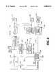
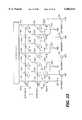
- FIG. 5is a block diagram of a multi-bit per cell EANVM system 100 in accordance with the present invention, which includes an M ⁇ N array of EANVM cells.
- the cellsare shown as floating gate FET cells 102, having the same construction as described in connection with FIG. 1.
- the general arrangement of the systemis similar to that used for conventional single-bit per cell memory devices, although on a detailed level there are significant differences related to the multi-bit per cell implementation as will be apparent later.
- Each cell 102 in FIG. 5belongs to a row and a column of the array and has its source connected to a ground reference potential and its drain connected to a corresponding column bit line 106.
- the column bit linesare connected to corresponding pull-up devices indicated collectively by the block 105. All control gates of a row of cells are connected to a corresponding row select, or word, line 104. Rows are selected with a row select circuit 108 and columns are selected with a column select circuit 110 in the usual manner. Row and column address signals are provided over corresponding address busses 103A and 103B. Sense amplifiers 112 are provided for each of the columns of the array.
- a PGM/Write signalis provided at an input terminal 118 for activating a mode control circuit 120 and a timing circuit 122.
- a significant advantage of this multi-bit per cell system 100 as compared to a single-bit per cell implementationis that the memory density is increased by a factor of n, where n is the number of bits which can be stored in an individual multi-bit memory cell.
- FIG. 6shows a binary system 150 for reading the state of multi-bit floating gate memory cell 102.
- the number of bits per cell (n)is assumed to be 2, so that one of four states of the memory cell must be detected, the four possible states being (0,0), (0,1), (1,0), and (1,1).
- a 4-level sense amplifier 152is provided. This amplifier includes three sense amplifiers 154, 156, and 158, each of which has its negative input terminal connected to the output terminal 138 of the memory cell 102.
- Sense amplifier 154has a reference voltage Ref3 connected to its positive input terminal
- sense amplifier 156has a reference voltage Ref2 connected to its positive input terminal
- sense amplifier 158has a reference voltage Ref1 connected to its positive input terminal.
- These reference voltagesdemarcate the four memory states of the cell 102 and are set so as to satisfy the relationship Vpull-up>Ref3>Ref2>Ref1 (preferred techniques for generating these reference voltages will be described later).
- the respective output signals S3, S2, S1 of the three sense amplifiersdrive an encode logic circuit 160, which encodes the sensed signals S3, S2, S1 into an appropriate 2-bit data format. Bit 0 is provided at an I/O terminal 162, and Bit 1 is provided at an I/O terminal 164.
- a truth table for the encode logic circuit 160is as follows:
- the levels of the respective output signals S3, S2, S1 of the sense amplifiers 154, 156, 158are determined by the conductivity value to which the memory cell has been set during a programming operation (to be described later).
- EANVM cell 102When fully erased, EANVM cell 102 will be in its lowest threshold voltage state--that is, the highest conductivity state. Consequently, all of the reference voltages will be higher than the bit line voltage at terminal 138, indicating a (1,1) state.
- EANVM cell 102When fully programmed, EANVM cell 102 will be in its highest threshold voltage state, that is, its lowest conductivity state. Consequently, all reference voltages will be lower than the bit line voltage at terminal 138, indicating a (0,0) state.
- the intermediate threshold statesare encoded as illustrated in the previous truth table for the logic circuit 160.
- FIG. 7shows the bit line voltage at terminal 138 as a function of time during a read cycle for the memory cell 102.
- each of the four possible voltage signals corresponding to the four possible programmed states of the memory cellare shown.
- the signal corresponding to the actual programmed state of the EANVM cellwould occur.
- the EANVM memory cell 102has been programmed to a (1,0) state.
- the bit line 106is pulled up to Vpull-up.
- the EANVM cellis selected using standard memory address decoding techniques.
- the bit lineis pulled down to a specific voltage level corresponding to the amount of current that the cell can sink at this specific conductivity level.
- the bit line voltagestabilizes at a voltage level Vref3 between reference voltages Ref 3 and Ref 2 which bound the (1,0) state.
- the bit line voltagewill return to its pulled-up condition.
- the bit-line voltagestabilizes at Vref2 for the (0,1) state or at 0 volts for the (1,1) state.
- FIG. 8is a block diagram of circuitry 200 for programming and reading memory cell 102. Although a binary 2-bit per cell system is shown for purposes of illustration, it is to be understood that the principles of the invention are similarly applicable to any system where the EANVM cell has more than two states. For example, in a non-binary system, the memory states can be three or some other multiple of a non-binary base.
- the system 200includes a memory cell 102 with a bit line output terminal 138.
- the 4-level sense amplifier 152supplied with read reference voltages Ref1, Ref2, and Ref3, and the encoder 160 are provided.
- Read datais provided at the Bit 0 I/O terminal 162 and at the Bit 1 I/O terminal 164.
- a verify reference select circuit 222provides an analog programming voltage reference level signal X to one input terminal of an analog comparator 202.
- the programming reference voltagesare chosen so that as soon as the bit line voltage on bit line 106 has reached the programming reference voltage level corresponding to a target memory state, the EANVM cell 102 is set to a proper threshold corresponding to the target memory state.
- the programming reference voltages Vref1, Vref2, Vref3, and Vref4are set such that Vref4 is above Ref3, Vref3 is between Ref3 and Ref2, Vref2 is between Ref1 and Ref2, and Vref1 is below Ref1.
- the bit line voltagewill thus settle substantially midway between the read reference voltages demarcating the intermediate state to insure that the memory contents will be read accurately.
- the verify reference select circuit 222is controlled by the two output bits from a 2-bit input latch/buffer circuit 224, which receives binary input bits from the I/O terminals 162 and 164.
- the Y signal input terminal of the analog comparator 202is connected to the bit line output terminal 138 of the multi-level memory cell 102.
- the output signal from the analog comparatoris provided on a signal line 204 as an enable/disable signal for a program voltage switch 220.
- An output signal line 206 from the program voltage switch 220provides the word line program voltage to the control gate of the EANVM cell 102.
- Another output signal line 106provides the bit line programming voltage to the bit line terminal 138 of EANVM cell 102.
- the timing circuit 208After the program/verify timing circuit 208 is enabled by a PGM/Write signal provided on signal line 212 from a PGM/Write terminal 214, the timing circuit 208 provides a series of program/verify timing pulses to the program voltage switch 220 on a signal line 210.
- the pulse widthsare set to control the programming process so that the voltage threshold of the EANVM cell 102 is incrementally altered by controlling the injection of charge onto the floating gate of the EANVM cell.
- Each programming cyclechanges the voltage threshold and, as a result, the conductivity of the memory cell 102.
- the program voltages provided by the program voltage switch 220After each internal program cycle is complete, as indicated by signal line 210 going "high", the program voltages provided by the program voltage switch 220 are removed, and a verify cycle begins.
- the voltage threshold of memory cell 102is then determined by using the comparator 202 to compare the bit line voltage at terminal 138 with the selected programming reference voltage from the verify reference select circuit 222. When the bit line voltage has reached the level of the programming reference voltage supplied by the verify reference select circuit 222, the output signal from the comparator on line 204 will disable the program voltage switch 220, ending the programming cycle.
- the analog comparator 202For this embodiment of the invention, during a write operation, comparison of the current memory cell analog contents with the analog information to be programmed on the memory cell 102 is performed by the analog comparator 202.
- the verify reference select circuit 222 analog output voltage Xis determined by decoding the output of the 2-bit input latch/buffer 224.
- the Y input signal to the analog comparator 202is taken directly from the bit line terminal 138.
- the 4-level sense/encode circuits 152, 160, and verify reference select circuit 222may be completely independent, as indicated in the drawing. Alternatively, they may be coupled together to alternately time share common circuit components. This is possible because the 4-level sense/encode circuits 152 and 160 are used in the read mode of operation while the verify reference select circuit 222 is used only in the write/verify mode of operation.
- nthe number of bits per cell.
- a first such thresholdis determined so that, in the read mode, the bit line voltage will fall between Ref1 and Ref2.
- Another such thresholdis determined so that, in the read mode, the bit line voltage will fall between Ref2 and Ref3.
- the third such thresholdis determined so that, in the read mode, the bit line voltage will be greater than Ref3.
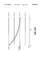
- FIG. 9illustrates the change in voltage threshold of a 4-level, or 2-bit, EANVM cell as the floating gate is being charged from an erased (1,1) threshold state to any one of the three other possible states (the charging being shown as continuous for simplicity).
- Vt1, Vt2, and Vt3 in FIG. 9are thresholds corresponding to the read reference levels Ref1, Ref2, and Ref3, respectively.
- the plots labeled (0,1), (1,0), and (0,0)correspond to the programming thresholds for those states, which are the three non-erased states.
- the design objectiveis to provide enough charge to the floating gate to insure that the cell's voltage threshold is programmed as high as possible, as shown in FIG. 3. Because there is no upper threshold limit in a single-bit per cell system, overprogramming the cell will not cause incorrect data to be stored on the memory cell.
- the memory cellin a multi-bit per cell system, the memory cell must be charged to a point so that the voltage threshold is within a specific voltage threshold range.
- the proper threshold rangeis defined as being above a threshold level Vt2 and as being below a threshold level Vt3.
- the prior art EANVM circuitryis modified to the arrangement shown in FIG. 8.
- the comparator in FIG. 8, incidentally,is preferably analog as shown. However, a digital comparator could be used.
- FIG. 10illustrates the voltage threshold of a 4-level, or 2-bit, EANVM cell as the floating gate is being erased from a (0,0) state (the erasing being shown as continuous for simplicity).
- the EANVM programming operating proceduremay call for a memory cell to be erased prior to being programmed. This erasure can be performed at the byte, block, or chip level and can be performed by electrical, UV, or other means. In this type of system, the cell would be completely erased to a (1,1) state prior to initiating a programming cycle. If a system has the capability to erase an individual memory cell, then it is not necessary to erase all of the cells of a group prior to initiating a programming operation. It is then possible to incrementally erase an individual memory cell as necessary to program the cell to the appropriate one of the voltage thresholds indicated by the plots labeled (1,0), (0,1), and (1,1).
- FIG. 11is a voltage threshold timing diagram which illustrates how the system of FIG. 8 programs the 2-bit EANVM cell 102 from an erased (1,1) state to a (1,0) state using the timing circuitry 208 to generate fixed-width timing pulses.
- a low logic level state of the PGM/Write signal on signal line 212enables the timing circuit 208.
- the timing circuit 208After being enabled at time t1, the timing circuit 208 provides an internal fixed-width low-level internal PGM timing pulse on signal line 210 to the program voltage switch 220. This pulse is output following an initial verify cycle which will be discussed in connection with FIG. 12.
- the bit line and word line program voltage outputs on lines 106 and 206will be raised to their respective programming voltage levels as indicated in FIG. 11.
- chargeis added to the floating gate of the memory cell 102.
- the programming voltagesare removed and a verify cycle begins.
- verify reference voltage Vref3is compared with the bit line voltage.
- This internally controlled program/verify cyclerepeats itself until the bit line voltage on terminal 138 has reached Vref3.
- t2the EANVM cell 102 is verified to have been programmed to a (1,0) state, and programming is halted by the comparator 222 providing a disable signal on signal line 204 to the program voltage switch 220.
- FIG. 12illustrates the bit line voltage of the 2-bit EANVM cell 102 as it is being programmed from the fully erased, or fully “on”, state (1,1) to the partially “off” state (1,0) using fixed-width program pulses.
- the program/verify timing circuit 208first initiates a verify cycle to determine the current status of the memory cell 102. This is indicated by the bit line voltage being pulled to a ground condition (corresponding to the erased state) from, in this example, Vpull-up, although prior to time t1, the bit line voltage could be pre-set to any voltage level. Once the cell has been determined to be in the erased state, the first program cycle is initiated.
- bit line voltagebeing pulled up to Vprogram.
- a verify cyclebegins. This is represented by the bit line voltage being pulled down to a point midway between ground potential and Ref1. During each successive verify cycle, the bit line voltage is observed to incrementally increase. This program/verify cycle continues until the bit line voltage has reached the selected programming reference voltage, in this case Vref3, which indicates a memory state of (1,0), at time t2.
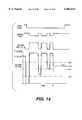
- FIG. 13illustrates how the 2-bit EANVM cell 102 is programmed from the erased (1,1) state to the (1,0) state using a timing circuit 208 that generates variable-width programming pulses.
- the internal PGM pulses for this implementationstart with a low state longer than for the fixed-width implementation of FIGS. 11 and 12.
- the low state pulse widthsgrow progressively shorter as the memory cell approaches the target voltage threshold. This approach requires more precise control than the fixed-width approach. However, programming times can be greatly reduced on average.
- FIG. 14illustrates the bit line voltage of cell 102 as it is being programmed from the fully erased, or fully “on”, state (1,1) to the partially “off” state (1,0) using variable length program pulses.
- the program/verify timing circuit 208first initiates a verify cycle to determine the current status of the memory cell 102. This is indicated by the bit line voltage being pulled to a ground condition (corresponding to the erased state) from, in this example, Vpull-up, although prior to time t1, the bit line voltage could be preset to any voltage level. Once the cell has been determined to be in the erased state, the first program cycle is initiated.
- the programming process for the multi-bit per cell EANVMuses program/verify cycles, to incrementally program the cell.
- the durations of these cyclesare determined by the timing circuit 208.
- a key element of the systemis to provide a programming scheme which provides for accurate programming of the memory cell 102. This is accomplished by matching the pulse widths of the timing pulses of the timing circuitry 208 to the program time of the EANVM cell being used. As seen from FIGS. 11 and 13, a desired voltage threshold actually falls within a range of threshold voltages. If the program pulses are too long, then too much charge may be added to the floating gate of the memory cell 102. This may result in an overshoot of the target voltage threshold, resulting in incorrect data being stored in the memory cell.
- the programming pulse widthis set such that if the voltage threshold of the cell 102 after the (N-l)Th programming pulse is at a point just below the target voltage threshold, then the (N)Th, or final, program pulse will not cause an overshoot resulting in an over programmed condition for a memory cell.
- the program and read circuitry in FIG. 8uses selectable programming reference voltage signals supplied to a bit line comparator to control programming of the multi-bit memory cell. Programming is accomplished without reading out the cell. This allows for a significant reduction in programming time relative to previous systems that require repeated readout of the memory state of the cell during the programming process.
- FIG. 8is not limited as to the manner in which the programming and read reference signals are established.
- the embodiments described in this sectionimplement important new concepts in memory state demarcation and programming control to enhance the reliability of the system.
- the embodiments for memory state demarcationare based on a new concept whereby the read reference signals are generated using the programming reference signals, or signals set in substantial correspondence with the programming reference signals.
- the read reference signalsare thus effectively dependent upon the programming reference signals. Because of this dependence, the system design can guarantee that the two sets of signals will closely conform with a predetermined relationship for program margining.
- the programming reference voltages of two adjacent memory statesmay be subjected to voltage division to generate the intervening read reference voltage. The read reference voltage will then fall midway between the two programming reference voltages. As a result, the two programming reference voltages are equally marginate from the read reference voltage.
- the embodiments related to programming controlparticularly address programming reference voltage generation. These embodiments employ reference cells which substantially track changes in operating characteristics of the memory cell (and thus its bit line signal) with changing conditions that affect the operating characteristics, such as temperature, system voltages, or mere passage of time.
- the use of such reference cellswhich preferably have the same (or at least in large part the same) construction as the memory cell, assures a stable relationship between the programming reference voltages and the operating characteristics of the memory cell.
- the read reference voltageswill also closely track the changes in operating characteristics of the memory cell. This assures that data stored in the memory cell over a long period of time can be read out accurately.
- An alternative to using the programming reference cells for this purposeis to use a separate group of reference cells to generate voltages substantially the same as the programming reference voltages. Using the voltages from the separate group of cells to generate the read reference voltages would provide a similar tracking effect of the read reference voltages.
- FIG. 15is a simplified diagram illustrating a circuit for generating the read reference voltages Ref1, Ref2, and Ref3.
- the read reference voltagesare generated by corresponding columns 1210, 1211, and 1212 of the circuit, each comprising a pair of reference cells connected in a voltage divider arrangement to generate the corresponding read reference signal.
- Column 1210includes a first pair of reference cells 1203, 1204 for generating voltage Ref1.
- Column 1211includes a second pair of reference cells 1205, 1206 for generating voltage Ref2.
- Column 1212includes a third pair of reference cells 1207, 1208 for generating voltage Ref3.
- a bit line column 1209The bit line column constitutes a portion of the main memory cell array and includes a memory cell 1202.
- reference cells 1203-1208 of the reference voltage generating circuitmay, in one preferred mode, be of the same type and construction as their associated memory cells (e.g., cell 1202) of the main array.
- all of the cells 1202-1208 in FIG. 15are assumed to be floating-gate-FET EANVM cells as previously described, all having the same construction.
- the reference cells, and indeed the reference columns,are preferably fabricated simultaneously with and by the same method as the columns of the main array, as part of the same integrated circuit with the array. Alternatively, the reference columns may be fabricated by way of the same method as the main memory cell array, but at a different time and/or as parts of a different integrated circuit.
- Each of the reference cells 1203-1208 in FIG. 15shares a common word (row select) line 1243 with the memory cell 1202.
- Each reference cellis also coupled, at its bit line, to a column pull-up voltage Vpull-up and the associated column output terminal via associated select transistors (FETs) 1201 and 1213, which may be NMOS or PMOS devices, for example.
- FETsselect transistors
- the select transistors 1201are controlled via respective select lines 1214'
- the select transistors 1213are controlled via respective select lines 1215'.
- the bit lines of each pair of reference cellsare connected together, as shown, to form the respective voltage divider arrangements.
- the memory cell 1202is also coupled to a column pull-up voltage and the associated column bit line output via a pair of select transistors 1201, 1213 controlled respectively by select lines 1214, 1215.
- the reference cells 1203-1208are pre-programmed at the factory to voltage thresholds corresponding to the programming reference voltages Vref1-Vref4. Specifically, reference cells 1203 and 1204 are programmed respectively to voltage thresholds V1 and V2 to produce voltages equal to programming reference voltages Vref1 and Vref2 on their respective bit lines. Reference cells 1205 and 1206 are respectively programmed to voltage thresholds V2 and V3 to produce voltages equal to programming reference voltages Vref2 and Vref3. Reference cells 1207 and 1208 are respectively programmed to voltage thresholds V3 and V4 to produce voltages equal to programming references Vref3 and Vref4. The programming of the reference cells may be accomplished in any suitable manner.
- the memory devicemay be provided with dedicated pins for external application of standard reference voltages to charge the cells.
- the memory devicemay incorporate an on-board set of ROM cells having implant dosages for providing bit line voltages corresponding to the desired programming reference voltages.
- the ROM bit line voltageswould be used as programming reference voltages for initially programming the EANVM reference cells.
- the EANVM reference cellscould be selectively coupled to the program verification comparator 202 (FIG. 8) to provide signal Y, and the ROM bit line voltages could be selectively applied to the comparator as signal X to program the EANVM reference cells by a programming operation as previously described. By using programming pulses of small width(s), the reference cells would be programmed with good accuracy.
- the ROM cellscould also be used to reprogram the EANVM reference cells (under predetermined standard conditions) to restore the voltage thresholds of the reference cells to design values, if necessary.
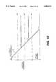
- the reference signal generating circuit shown in FIG. 15establishes relationships between the programming reference voltages and the read reference voltages as shown in FIG. 16. It should be noted that the assignment of particular memory states to the programming reference voltages Vref1-Vref4 is not a critical matter, although good design practice dictates that the assignments should be consistent throughout the memory system. In a system employing error correction, it may be advantageous to assign the memory states out of binary sequence to facilitate optimization of error detection and correction algorithms. The present discussion assumes assignment of the memory states to the programming reference voltages in a non-binary sequence.
- memory state (1,1)is assigned to the first (lowest) programming reference voltage Vref1
- memory state (0,1)is assigned to the second programming reference voltage Vref2
- memory state (1,0)is assigned to the third programming reference voltage Vref3
- memory state (0,0)is assigned to the fourth (highest) programming reference voltage Vref4.
- each read reference voltageis established so that the programming reference voltages for the memory states immediately above and below are equally margined relative to the read reference voltage. More particularly, the read reference voltages are defined as follows:
- each read reference levelwill always be optimally margined relative to the adjacent programming reference levels at a position midway between the programming reference levels.
- the operating characteristics of the reference cellstrack variations in the operating characteristics of the memory cell with changing conditions that affect the operating characteristics, the relationships shown in FIG. 16 are maintained throughout such variations. This ensures that data stored in the memory cell over a long period of time can be read out accurately despite differences in temperature, system voltages, etc. at the time of readout relative to the time of data storage.
- the curve shown in FIG. 16indicates the bit line voltage of the memory cell during readout, assuming the cell is programmed to programming reference voltage Vref1.
- Deviationsmay occur, for example, due to asymmetries in the physical arrangement of the circuit components, which are ordinarily laid out to maximize the compactness of the integrated circuit. Such asymmetries may result in differing line lengths and capacitance effects, for example, relative to the individual reference cells of a given pair.
- the deviationscan be determined in advance by computer simulation of the circuit using standard computer simulation techniques. It is then possible to compensate for the deviations by adding appropriate signal pulling devices on the read reference lines to pull the divided outputs of the reference cells to the design values. Such devices may also be provided for similar reasons on the memory cell bit lines of the main array.
- FIG. 17shows a read-reference signal generating circuit as just described.
- the circuitis identical to that of FIG. 15, except for the addition of the aforementioned signal pulling devices.
- These devicesmay be constituted by field effect transistors 1220-1223, as shown, or by any other suitable type of device for this purpose, such as capacitor and resistor combinations, etc.
- the signal pulling devicesare preferably connected as closely as possible to the points where the read reference signals (and memory bit line signals) feed into the multi-level sense amplifier for reading out the memory cell. Such an arrangement will optimize the accuracy of the voltage values supplied to the sense amplifier relative to the design values. This is, of course, desirable from the standpoint of high accuracy program margining and memory readout.
- FIG. 18is a simplified diagram showing another embodiment of a circuit 1200" for generating the read reference signals Ref1, Ref2, and Ref3
- This circuitis based on the design of the circuit in FIG. 17, but the higher-value reference cell and signal puller of each reference column are replaced by a corresponding single pull-up device 1321, 1322, or 1323 to provide the voltage divider arrangements, as shown.
- the pull-up devices on the individual read reference lines in FIG. 18have their respective signal-pulling capacities set so that the read reference voltages will assume the same relationships relative to the programming reference voltages as shown in FIG. 16. It should be noted that this embodiment is less preferred than the arrangement of FIG. 17 from the standpoint of tracking the memory cell, since the pull-up devices 1321, 1322, and 1323 on the read reference lines will not track the memory cell 1202 as closely as the reference cells with changing operating conditions.
- FIG. 19is a more generalized diagram illustrating how the reference signal generating circuit of FIG. 15 can be applied to a memory array.
- the select line 1214 and select transistors 1201which are not required but may be desirable to reduce energy consumption, for example, have been replaced by a generic network of column pull-ups (so designated).
- each row of memory cells in the arrayis provided with a corresponding set of reference cells 1203-1208 connected to form voltage divider arrangements as previously described.
- Each set (row) of reference cellswould be selected individually for providing signals on the reference column bit lines for readout of a memory cell of the corresponding row of the main array.
- the use of dedicated sets of reference cells for each row of the arrayis preferred for accuracy. More particularly, the use of dedicated reference cells allows for better symmetry in the arrangement of each set of reference cells relative to that of the corresponding row of memory cells within the overall memory circuit.
- a reference cell for row M of the memory array in FIG. 20will have the same number and type of components connected between its bit line terminal and the reference column output as does each corresponding memory cell 1202 between its bit line terminal and the column bit line output.
- the line length from the bit line terminal of the reference cell to the reference column outputcan made close to or the same as the line length from the bit line terminal of each corresponding memory cell to its associated column bit line output.
- Signal pulling devicesmay be added on the bit and read reference lines in a manner similar to FIG. 17. In this case, the signal pulling capacity of each device would be determined by suitable calculation during the computer simulation process to provide the best overall accuracy of the signal levels provided by the different cells within each column of the system.
- FIG. 20is a simplified diagram showing a circuit 1500 (above the dashed line) for generating programming references Vref1-Vref4 and an associated verify reference select circuit 222 (below the dashed line) for outputting the selected signal X for program verification.
- each row of the memory arrayis coupled with a set of reference cells 1503-1506 having the same construction as the memory cells.
- the reference cellsneed not be part of the same integrated circuit as the memory array, but they are preferably fabricated simultaneously with and by the same process as the array, as part of the same integrated circuit, for the reasons previously explained.
- the use of a dedicated set of programming reference cells for each row of the arrayis preferable for the same reasons as were discussed in connection with the arrangement of FIG. 20.
- the reference cells for producing the programming reference signals Vref1-Vref4are arranged in corresponding columns 1511-1514, with their bit line terminals commonly connected to a corresponding bit line and a network of column pull-ups (so designated). Each set (row) of reference cells would be individually selected, via an associated word line 1543, for providing signals on the corresponding column bit lines for programming verification of a memory cell of the corresponding row of the main memory array.
- Each reference cell 1503 in column 1511is pre-programmed at the factory (for example, as previously described in connection with FIG. 15) to the voltage threshold V1 to produce voltage Vref1 on the column bit line.
- Each reference cell 1504 in column 1512is pre-programmed to the voltage threshold V2 to produce voltage Vref2 on the column bit line.
- Each reference cell in column 1513is pre-programmed to the voltage threshold V3 to produce voltage Vref3 on the column bit line.
- Each reference cell in column 1514is pre-programmed to the voltage threshold V4 to produce voltage Vref4 on the column bit line.
- Signal pulling devicesmay be added on the column bit lines as previously explained if necessary to compensate for deviations of the column bit line voltages due to effects of layout asymmetries and the like.
- the bit lines of columns 1511-1514are coupled to corresponding select transistors (e.g., FETs) 271-274 of verify reference select circuit 222.
- the select transistorswhich may be NMOS or PMOS devices, for example, can be controlled by a simple logic circuit, such as the logic circuit LC shown in FIG. 20.
- the circuit LC in FIG. 20operates in accordance with the following truth table. Note that the signals I/O0 and I/O1 are provided as inputs from the input latch/buffer 224 (see FIG. 8).
- FIGS. 21A-21Dare readout timing diagrams showing the bit line voltage level of a selected memory cell in FIG. 20 after programming to each of the four memory states.
- the bit line voltageis at its pre-charged value of Vpull-up, which is at or very near the value of Vref4.
- the voltage levelhas dropped to the range indicated by the two closely spaced lines which are centered around the Vref level for the programmed state. The two lines indicate that there is a slight range of tolerance for the bit line voltage level relative to the programming voltage reference level during read out of the memory cell.
- FIG. 21Aillustrates the bit line voltage when the memory cell has been programmed to the voltage threshold V1 corresponding to the programming reference level Vref1.
- FIG. 21Billustrates the bit line voltage when the memory cell has been programmed to the voltage threshold V2 corresponding to the programming reference level Vref2.
- FIG. 21Cillustrates the bit line voltage when the memory cell has been programmed to the voltage threshold V3 corresponding to the programming reference level Vref3.
- FIG. 21Dillustrates the bit line voltage when the memory cell has been programmed to the voltage threshold V4 corresponding to the programming reference level Vref4.
- the read reference and programming reference generating circuitshave been shown and described as separate circuits above, the circuits may readily be combined to share components as shown in FIG. 22. This is possible because the programming reference signals and the read reference signals need not be used at the same time. More particularly, the programming reference signals need only be used during the memory cell programming operation, whereas the read reference signals need only be used during the memory cell readout operation.
- the circuit shown in FIG. 22is a modification of the circuit of FIG. 19.
- the bit line of reference cells 1203is connected to provide programming reference voltage Vref1
- the bit line of reference cells 1204is connected to provide programming reference voltage Vref2
- the bit line of reference cells 1207is connected to provide programming reference voltage Vref3
- the bit line of reference cells 1208is connected to provide programming reference voltage Vref4.
- Select transistors 271-274correspond to the select transistors shown in FIG. 20.
- FIG. 23shows a modification of the circuit in FIG. 22, in which the EANVM reference cells 1203-1208 are replaced by ROM cells 2203-2208, respectively.
- ROM cellsas reference cells is advantageous because it avoids the initial programming requirement of EANVM reference cells, although the tracking effect of the reference signals relative to the EANVM cells of the main array may be reduced somewhat.
- corresponding portions of the ROM cells and the EANVM cellscan be fabricated by the same process steps. For example, the sources, drains, channel regions, and control gates of the EANVM cells and the ROM cells may be fabricated in this manner, with separate process steps being used to provide the EANVM floating gates and the ROM threshold implants.
Landscapes
- Engineering & Computer Science (AREA)
- Computer Hardware Design (AREA)
- Read Only Memory (AREA)
Abstract
Description
______________________________________ S3 S2 S1 I/O 1 I/O 0 State ______________________________________L L L 0 0 (0,0) H L L 1 (1,0) H H L 0 (0,1) H H H 1 (1,1) ______________________________________
______________________________________ I/O 0 I/O 1 Vref1 Select Vref2 Select Vref3 Select Vref4 Select ______________________________________ 0 0L L L H 1 0L L 0 1L L 1 1 H L ______________________________________
Claims (77)
Priority Applications (26)
| Application Number | Priority Date | Filing Date | Title |
|---|---|---|---|
| US08/975,919US6002614A (en) | 1991-02-08 | 1997-11-21 | Memory apparatus including programmable non-volatile multi-bit memory cell, and apparatus and method for demarcating memory states of the cell |
| JP2000522592AJP3693915B2 (en) | 1997-11-21 | 1997-12-11 | Storage device having programmable non-volatile multi-bit memory cell and device and method for demarcating storage state of the cell |
| DE69736493TDE69736493T2 (en) | 1997-11-21 | 1997-12-11 | Memory device with programmable non-volatile multi-bit memory cell and apparatus and method for delimiting memory states of the cell |
| AU56009/98AAU5600998A (en) | 1997-11-21 | 1997-12-11 | Memory apparatus including programmable non-volatile multi-bit memory cell, and apparatus and method for demarcating memory states of the cell |
| EP06118606AEP1715490A1 (en) | 1997-11-21 | 1997-12-11 | A non-volatile semiconductor memory |
| EP01126898AEP1211692B1 (en) | 1997-11-21 | 1997-12-11 | Memory apparatus including programmable non-volatile multi-bit memory cell, and apparatus and method for demarcating memory states of the cell |
| AT01126898TATE336069T1 (en) | 1997-11-21 | 1997-12-11 | MEMORY DEVICE WITH A PROGRAMMABLE NON-VOLATILE MULTI-BIT MEMORY CELL AND DEVICE AND METHOD FOR DETERMINING MEMORY STATES OF THE CELL |
| KR10-2000-7005519AKR100518494B1 (en) | 1991-02-08 | 1997-12-11 | Non-volatile semiconductor memory device |
| EP97952391AEP1032938A1 (en) | 1997-11-21 | 1997-12-11 | Memory apparatus including programmable non-volatile multi-bit memory cell, and apparatus and method for demarcating memory states of the cell |
| EP10185592AEP2273507A3 (en) | 1997-11-21 | 1997-12-11 | Memory apparatus including programmable non-volatile multi-bit memory cell, and apparatus for demarcating memory states of the cell |
| KR10-2001-7015722AKR100518499B1 (en) | 1991-02-08 | 1997-12-11 | Memory apparatus including programmable non-volatile multi-bit memory cell, and apparatus and method for demarcating memory states of the cell |
| PCT/US1997/022809WO1999027539A1 (en) | 1997-11-21 | 1997-12-11 | Memory apparatus including programmable non-volatile multi-bit memory cell, and apparatus and method for demarcating memory states of the cell |
| US09/311,749US6011716A (en) | 1991-02-08 | 1999-05-14 | Memory apparatus including programmable non-volatile multi-bit memory cell, and apparatus and method for demarcating memory states of the cell |
| US09/311,750US6118692A (en) | 1991-02-08 | 1999-05-14 | Memory apparatus including programmable non-volatile multi-bit memory cell, and apparatus and method for demarcating memory states of the cell |
| US09/311,748US6014327A (en) | 1991-02-08 | 1999-05-14 | Memory apparatus including programmable non-volatile multi-bit memory cell, and apparatus and method for demarcating memory states of the cell |
| US09/411,315US6246613B1 (en) | 1991-02-08 | 1999-10-04 | Memory apparatus including programmable non-volatile multi-bit memory cell, and apparatus and method for demarcating memory states of the cell |
| US09/733,937US6353554B1 (en) | 1995-02-27 | 2000-12-12 | Memory apparatus including programmable non-volatile multi-bit memory cell, and apparatus and method for demarcating memory states of the cell |
| US09/893,545US6434050B2 (en) | 1995-02-27 | 2001-06-29 | Memory apparatus including programmable non-volatile multi-bit memory cell, and apparatus and method for demarcating memory states of the cell |
| US09/894,134US6381172B2 (en) | 1995-02-27 | 2001-06-29 | Memory apparatus including programmable non-volatile multi-bit memory cell, and apparatus and method for demarcating memory states of the cell |
| JP2002132946AJP3735082B2 (en) | 1997-11-21 | 2002-05-08 | Storage device having programmable non-volatile multi-bit memory cell and device and method for demarcating storage state of the cell |
| US10/188,835US6714455B2 (en) | 1995-02-27 | 2002-07-05 | Memory apparatus including programmable non-volatile multi-bit memory cell, and apparatus and method for demarcating memory states of the cell |
| US10/742,890US7006384B2 (en) | 1995-02-27 | 2003-12-23 | Memory apparatus including programmable non-volatile multi-bit memory cell, and apparatus and method for demarcating memory states of the cell |
| US10/944,194US7068542B2 (en) | 1995-02-27 | 2004-09-20 | Memory apparatus including programmable non-volatile multi-bit memory cell, and apparatus and method for demarcating memory states of the cell |
| US11/407,148US7286414B2 (en) | 1995-02-27 | 2006-04-20 | Memory apparatus including programmable non-volatile multi-bit memory cell, and apparatus and method for demarcating memory states of the cell |
| US11/876,683US7911851B2 (en) | 1995-02-27 | 2007-10-22 | Memory apparatus including programmable non-volatile multi-bit memory cell, and apparatus and method for demarcating memory states of the cell |
| US13/041,340US8570814B2 (en) | 1995-02-27 | 2011-03-04 | Memory apparatus including programmable non-volatile multi-bit memory cell, and apparatus and method for demarcating memory states of the cell |
Applications Claiming Priority (4)
| Application Number | Priority Date | Filing Date | Title |
|---|---|---|---|
| US07/652,878US5218569A (en) | 1991-02-08 | 1991-02-08 | Electrically alterable non-volatile memory with n-bits per memory cell |
| US08/071,816US5394362A (en) | 1991-02-08 | 1993-06-04 | Electrically alterable non-voltatile memory with N-bits per memory cell |
| US08/410,200US5764571A (en) | 1991-02-08 | 1995-02-27 | Electrically alterable non-volatile memory with N-bits per cell |
| US08/975,919US6002614A (en) | 1991-02-08 | 1997-11-21 | Memory apparatus including programmable non-volatile multi-bit memory cell, and apparatus and method for demarcating memory states of the cell |
Related Parent Applications (1)
| Application Number | Title | Priority Date | Filing Date |
|---|---|---|---|
| US08/410,200Continuation-In-PartUS5764571A (en) | 1991-02-08 | 1995-02-27 | Electrically alterable non-volatile memory with N-bits per cell |
Related Child Applications (4)
| Application Number | Title | Priority Date | Filing Date |
|---|---|---|---|
| US09/311,749DivisionUS6011716A (en) | 1991-02-08 | 1999-05-14 | Memory apparatus including programmable non-volatile multi-bit memory cell, and apparatus and method for demarcating memory states of the cell |
| US09/311,750DivisionUS6118692A (en) | 1991-02-08 | 1999-05-14 | Memory apparatus including programmable non-volatile multi-bit memory cell, and apparatus and method for demarcating memory states of the cell |
| US09/311,748DivisionUS6014327A (en) | 1991-02-08 | 1999-05-14 | Memory apparatus including programmable non-volatile multi-bit memory cell, and apparatus and method for demarcating memory states of the cell |
| US09/411,315DivisionUS6246613B1 (en) | 1991-02-08 | 1999-10-04 | Memory apparatus including programmable non-volatile multi-bit memory cell, and apparatus and method for demarcating memory states of the cell |
Publications (1)
| Publication Number | Publication Date |
|---|---|
| US6002614Atrue US6002614A (en) | 1999-12-14 |
Family
ID=27371972
Family Applications (5)
| Application Number | Title | Priority Date | Filing Date |
|---|---|---|---|
| US08/975,919Expired - LifetimeUS6002614A (en) | 1991-02-08 | 1997-11-21 | Memory apparatus including programmable non-volatile multi-bit memory cell, and apparatus and method for demarcating memory states of the cell |
| US09/311,749Expired - Fee RelatedUS6011716A (en) | 1991-02-08 | 1999-05-14 | Memory apparatus including programmable non-volatile multi-bit memory cell, and apparatus and method for demarcating memory states of the cell |
| US09/311,748Expired - Fee RelatedUS6014327A (en) | 1991-02-08 | 1999-05-14 | Memory apparatus including programmable non-volatile multi-bit memory cell, and apparatus and method for demarcating memory states of the cell |
| US09/311,750Expired - Fee RelatedUS6118692A (en) | 1991-02-08 | 1999-05-14 | Memory apparatus including programmable non-volatile multi-bit memory cell, and apparatus and method for demarcating memory states of the cell |
| US09/411,315Expired - Fee RelatedUS6246613B1 (en) | 1991-02-08 | 1999-10-04 | Memory apparatus including programmable non-volatile multi-bit memory cell, and apparatus and method for demarcating memory states of the cell |
Family Applications After (4)
| Application Number | Title | Priority Date | Filing Date |
|---|---|---|---|
| US09/311,749Expired - Fee RelatedUS6011716A (en) | 1991-02-08 | 1999-05-14 | Memory apparatus including programmable non-volatile multi-bit memory cell, and apparatus and method for demarcating memory states of the cell |
| US09/311,748Expired - Fee RelatedUS6014327A (en) | 1991-02-08 | 1999-05-14 | Memory apparatus including programmable non-volatile multi-bit memory cell, and apparatus and method for demarcating memory states of the cell |
| US09/311,750Expired - Fee RelatedUS6118692A (en) | 1991-02-08 | 1999-05-14 | Memory apparatus including programmable non-volatile multi-bit memory cell, and apparatus and method for demarcating memory states of the cell |
| US09/411,315Expired - Fee RelatedUS6246613B1 (en) | 1991-02-08 | 1999-10-04 | Memory apparatus including programmable non-volatile multi-bit memory cell, and apparatus and method for demarcating memory states of the cell |
Country Status (1)
| Country | Link |
|---|---|
| US (5) | US6002614A (en) |
Cited By (32)
| Publication number | Priority date | Publication date | Assignee | Title |
|---|---|---|---|---|
| US6424568B2 (en) | 1999-12-28 | 2002-07-23 | Hyundai Electronics Industries Co., Ltd. | Code addressable memory cell in flash memory device |
| US6466476B1 (en) | 2001-01-18 | 2002-10-15 | Multi Level Memory Technology | Data coding for multi-bit-per-cell memories having variable numbers of bits per memory cell |
| US6515904B2 (en) | 2001-03-21 | 2003-02-04 | Matrix Semiconductor, Inc. | Method and system for increasing programming bandwidth in a non-volatile memory device |
| US6532556B1 (en) | 2000-01-27 | 2003-03-11 | Multi Level Memory Technology | Data management for multi-bit-per-cell memories |
| US6538922B1 (en) | 2000-09-27 | 2003-03-25 | Sandisk Corporation | Writable tracking cells |
| US6574145B2 (en) | 2001-03-21 | 2003-06-03 | Matrix Semiconductor, Inc. | Memory device and method for sensing while programming a non-volatile memory cell |
| US20030103406A1 (en)* | 1999-01-14 | 2003-06-05 | Tran Hieu Van | Digital multilevel memory system having multistage autozero sensing |
| US20030103400A1 (en)* | 1999-01-14 | 2003-06-05 | Hieu Van Tran | Multistage autozero sensing for a multilevel non-volatile memory integrated circuit system |
| US20030103398A1 (en)* | 1999-01-14 | 2003-06-05 | Hieu Van Tran | Sub-volt sensing for digital multilevel flash memory |
| US6584012B2 (en) | 1991-02-08 | 2003-06-24 | Btg International Inc. | Electrically alterable non-volatile memory with N-bits per cell |
| US20030159014A1 (en)* | 2001-12-28 | 2003-08-21 | Stmicroelectronics S.R.L. | Programming method for a multilevel memory cell |
| US20030161183A1 (en)* | 1999-01-14 | 2003-08-28 | Tran Hieu Van | Digital multilevel non-volatile memory system |
| US6662263B1 (en) | 2000-03-03 | 2003-12-09 | Multi Level Memory Technology | Sectorless flash memory architecture |
| US6714455B2 (en) | 1995-02-27 | 2004-03-30 | Btg International Inc. | Memory apparatus including programmable non-volatile multi-bit memory cell, and apparatus and method for demarcating memory states of the cell |
| US6751118B2 (en)* | 1999-01-14 | 2004-06-15 | Silicon Storage Technology, Inc. | Array architecture and operating methods for digital multilevel nonvolatile memory integrated circuit system |
| US20040255090A1 (en)* | 2003-06-13 | 2004-12-16 | Guterman Daniel C. | Tracking cells for a memory system |
| US6834331B1 (en)* | 2000-10-24 | 2004-12-21 | Starfish Software, Inc. | System and method for improving flash memory data integrity |
| US20050006692A1 (en)* | 2003-07-10 | 2005-01-13 | Kim Moo-Sung | Flash memory device |
| US6985372B1 (en)* | 2002-04-23 | 2006-01-10 | Alta Analog, Inc. | Analog content addressable memory (CAM) employing analog nonvolatile storage |
| US20060126387A1 (en)* | 2004-12-15 | 2006-06-15 | Dae-Han Kim | Multi-level cell memory device and associated read method |
| US20060268621A1 (en)* | 2001-04-05 | 2006-11-30 | Saifun Semiconductors, Ltd. | Method for programming a reference cell |
| US20070025157A1 (en)* | 2005-08-01 | 2007-02-01 | Jun Wan | Method for programming non-volatile memory with self-adjusting maximum program loop |
| US7301807B2 (en) | 2003-10-23 | 2007-11-27 | Sandisk Corporation | Writable tracking cells |
| US20080037322A1 (en)* | 1997-05-28 | 2008-02-14 | Kunihiro Katayama | Semiconductor memory having electrically erasable and programmable semiconductor memory cells |
| US20080055984A1 (en)* | 2006-08-31 | 2008-03-06 | Micron Technology, Inc. | Non-volatile memory device and method having bit-state assignments selected to minimize signal coupling |
| KR100816171B1 (en)* | 2001-12-17 | 2008-03-24 | 주식회사 하이닉스반도체 | How to erase data in flash memory cells |
| US20090066547A1 (en)* | 2007-09-07 | 2009-03-12 | Vishal Sarin | Analog-to-digital and digital-to-analog conversion window adjustment based on reference cells in a memory device |
| US7701779B2 (en)* | 2006-04-27 | 2010-04-20 | Sajfun Semiconductors Ltd. | Method for programming a reference cell |
| US9754645B2 (en)* | 2015-10-27 | 2017-09-05 | Sandisk Technologies Llc | Bit line charging for a device |
| US20170337974A1 (en)* | 2008-01-25 | 2017-11-23 | Micron Technology, Inc. | Random telegraph signal noise reduction scheme for semiconductor memories |
| US10026489B2 (en)* | 2016-03-08 | 2018-07-17 | SK Hynix Inc. | Semiconductor memory device and operating method thereof |
| US20220336028A1 (en)* | 2021-04-19 | 2022-10-20 | Micron Technology, Inc. | Dual verify for quick charge loss reduction in memory cells |
Families Citing this family (60)
| Publication number | Priority date | Publication date | Assignee | Title |
|---|---|---|---|---|
| US7447069B1 (en) | 1989-04-13 | 2008-11-04 | Sandisk Corporation | Flash EEprom system |
| EP0935255A2 (en)* | 1989-04-13 | 1999-08-11 | SanDisk Corporation | Flash EEPROM system |
| IL125604A (en) | 1997-07-30 | 2004-03-28 | Saifun Semiconductors Ltd | Non-volatile electrically erasable and programmble semiconductor memory cell utilizing asymmetrical charge |
| US6768165B1 (en) | 1997-08-01 | 2004-07-27 | Saifun Semiconductors Ltd. | Two bit non-volatile electrically erasable and programmable semiconductor memory cell utilizing asymmetrical charge trapping |
| KR100266748B1 (en)* | 1997-12-31 | 2000-10-02 | 윤종용 | Semiconductor memory device and error correction method thereof |
| US6490204B2 (en)* | 2000-05-04 | 2002-12-03 | Saifun Semiconductors Ltd. | Programming and erasing methods for a reference cell of an NROM array |
| US6396741B1 (en) | 2000-05-04 | 2002-05-28 | Saifun Semiconductors Ltd. | Programming of nonvolatile memory cells |
| US6928001B2 (en) | 2000-12-07 | 2005-08-09 | Saifun Semiconductors Ltd. | Programming and erasing methods for a non-volatile memory cell |
| JP2002063793A (en)* | 2000-08-18 | 2002-02-28 | Fujitsu Ltd | Readout device and readout method for semiconductor storage device |
| EP1199725B1 (en)* | 2000-10-13 | 2010-10-06 | STMicroelectronics Srl | Method for storing and reading data in a multibit nonvolatile memory with a non-binary number of bits per cell |
| TW478153B (en)* | 2000-11-23 | 2002-03-01 | Macronix Int Co Ltd | Automatic voltage regulator of embedded flash memory |
| US6738289B2 (en)* | 2001-02-26 | 2004-05-18 | Sandisk Corporation | Non-volatile memory with improved programming and method therefor |
| TWI230392B (en)* | 2001-06-18 | 2005-04-01 | Innovative Silicon Sa | Semiconductor device |
| TWI239251B (en) | 2001-07-31 | 2005-09-11 | Chrysalis Tech Inc | Method and apparatus for generating a volatilized liquid |
| EP1298670B1 (en)* | 2001-09-28 | 2007-03-07 | STMicroelectronics S.r.l. | Method for storing and reading data in a multilevel nonvolatile memory with a non-binary number of levels, and architecture therefor |
| US6700818B2 (en)* | 2002-01-31 | 2004-03-02 | Saifun Semiconductors Ltd. | Method for operating a memory device |
| US7190620B2 (en)* | 2002-01-31 | 2007-03-13 | Saifun Semiconductors Ltd. | Method for operating a memory device |
| US6975536B2 (en)* | 2002-01-31 | 2005-12-13 | Saifun Semiconductors Ltd. | Mass storage array and methods for operation thereof |
| US6917544B2 (en) | 2002-07-10 | 2005-07-12 | Saifun Semiconductors Ltd. | Multiple use memory chip |
| US6618297B1 (en) | 2002-08-02 | 2003-09-09 | Atmel Corporation | Method of establishing reference levels for sensing multilevel memory cell states |
| US6963505B2 (en) | 2002-10-29 | 2005-11-08 | Aifun Semiconductors Ltd. | Method circuit and system for determining a reference voltage |
| US7136304B2 (en) | 2002-10-29 | 2006-11-14 | Saifun Semiconductor Ltd | Method, system and circuit for programming a non-volatile memory array |
| US6992932B2 (en) | 2002-10-29 | 2006-01-31 | Saifun Semiconductors Ltd | Method circuit and system for read error detection in a non-volatile memory array |
| US6967896B2 (en) | 2003-01-30 | 2005-11-22 | Saifun Semiconductors Ltd | Address scramble |
| US7178004B2 (en) | 2003-01-31 | 2007-02-13 | Yan Polansky | Memory array programming circuit and a method for using the circuit |
| US7142464B2 (en) | 2003-04-29 | 2006-11-28 | Saifun Semiconductors Ltd. | Apparatus and methods for multi-level sensing in a memory array |
| US6954393B2 (en)* | 2003-09-16 | 2005-10-11 | Saifun Semiconductors Ltd. | Reading array cell with matched reference cell |
| US7123532B2 (en) | 2003-09-16 | 2006-10-17 | Saifun Semiconductors Ltd. | Operating array cells with matched reference cells |
| WO2005094178A2 (en) | 2004-04-01 | 2005-10-13 | Saifun Semiconductors Ltd. | Method, circuit and systems for erasing one or more non-volatile memory cells |
| US7755938B2 (en)* | 2004-04-19 | 2010-07-13 | Saifun Semiconductors Ltd. | Method for reading a memory array with neighbor effect cancellation |
| US7366025B2 (en)* | 2004-06-10 | 2008-04-29 | Saifun Semiconductors Ltd. | Reduced power programming of non-volatile cells |
| US7317633B2 (en) | 2004-07-06 | 2008-01-08 | Saifun Semiconductors Ltd | Protection of NROM devices from charge damage |
| US7095655B2 (en) | 2004-08-12 | 2006-08-22 | Saifun Semiconductors Ltd. | Dynamic matching of signal path and reference path for sensing |
| US7638850B2 (en) | 2004-10-14 | 2009-12-29 | Saifun Semiconductors Ltd. | Non-volatile memory structure and method of fabrication |
| US7535765B2 (en) | 2004-12-09 | 2009-05-19 | Saifun Semiconductors Ltd. | Non-volatile memory device and method for reading cells |
| US7257025B2 (en)* | 2004-12-09 | 2007-08-14 | Saifun Semiconductors Ltd | Method for reading non-volatile memory cells |
| EP1686592A3 (en) | 2005-01-19 | 2007-04-25 | Saifun Semiconductors Ltd. | Partial erase verify |
| US8053812B2 (en)* | 2005-03-17 | 2011-11-08 | Spansion Israel Ltd | Contact in planar NROM technology |
| JP4801935B2 (en) | 2005-06-08 | 2011-10-26 | 株式会社東芝 | Semiconductor memory device |
| US8400841B2 (en) | 2005-06-15 | 2013-03-19 | Spansion Israel Ltd. | Device to program adjacent storage cells of different NROM cells |
| US7184313B2 (en) | 2005-06-17 | 2007-02-27 | Saifun Semiconductors Ltd. | Method circuit and system for compensating for temperature induced margin loss in non-volatile memory cells |
| US7656710B1 (en) | 2005-07-14 | 2010-02-02 | Sau Ching Wong | Adaptive operations for nonvolatile memories |
| US7786512B2 (en) | 2005-07-18 | 2010-08-31 | Saifun Semiconductors Ltd. | Dense non-volatile memory array and method of fabrication |
| US7668017B2 (en) | 2005-08-17 | 2010-02-23 | Saifun Semiconductors Ltd. | Method of erasing non-volatile memory cells |
| US7221138B2 (en)* | 2005-09-27 | 2007-05-22 | Saifun Semiconductors Ltd | Method and apparatus for measuring charge pump output current |
| US7352627B2 (en) | 2006-01-03 | 2008-04-01 | Saifon Semiconductors Ltd. | Method, system, and circuit for operating a non-volatile memory array |
| US7808818B2 (en) | 2006-01-12 | 2010-10-05 | Saifun Semiconductors Ltd. | Secondary injection for NROM |
| US8253452B2 (en) | 2006-02-21 | 2012-08-28 | Spansion Israel Ltd | Circuit and method for powering up an integrated circuit and an integrated circuit utilizing same |
| US7692961B2 (en) | 2006-02-21 | 2010-04-06 | Saifun Semiconductors Ltd. | Method, circuit and device for disturb-control of programming nonvolatile memory cells by hot-hole injection (HHI) and by channel hot-electron (CHE) injection |
| US7760554B2 (en) | 2006-02-21 | 2010-07-20 | Saifun Semiconductors Ltd. | NROM non-volatile memory and mode of operation |
| US7638835B2 (en)* | 2006-02-28 | 2009-12-29 | Saifun Semiconductors Ltd. | Double density NROM with nitride strips (DDNS) |
| US7605579B2 (en) | 2006-09-18 | 2009-10-20 | Saifun Semiconductors Ltd. | Measuring and controlling current consumption and output current of charge pumps |
| KR100855971B1 (en)* | 2007-01-23 | 2008-09-02 | 삼성전자주식회사 | Memory cell programming method and semiconductor memory device that can program data into memory cell without initial read operation |
| KR101301773B1 (en)* | 2007-10-25 | 2013-09-02 | 삼성전자주식회사 | Apparatus and method of multi-bit programming |
| KR101057725B1 (en)* | 2008-12-31 | 2011-08-18 | 주식회사 하이닉스반도체 | Multi-level cell data sensing device and method thereof |
| JP5375253B2 (en)* | 2009-03-26 | 2013-12-25 | トヨタ自動車株式会社 | Vehicle shift control device |
| KR101024134B1 (en)* | 2009-06-12 | 2011-03-22 | 주식회사 하이닉스반도체 | Nonvolatile Memory Device and Its Program Method |
| US10832769B2 (en)* | 2018-12-26 | 2020-11-10 | Micron Technology, Inc. | Memory device with a charge transfer device |
| USD1045297S1 (en)* | 2020-08-14 | 2024-10-01 | Irobot Corporation | Mobile cleaning robot |
| US12230333B2 (en)* | 2022-09-28 | 2025-02-18 | Sandisk Technologies Llc | Bit line modulation to compensate for cell source variation |
Citations (102)
| Publication number | Priority date | Publication date | Assignee | Title |
|---|---|---|---|---|
| US3660819A (en)* | 1970-06-15 | 1972-05-02 | Intel Corp | Floating gate transistor and method for charging and discharging same |
| US3755721A (en)* | 1970-06-15 | 1973-08-28 | Intel Corp | Floating gate solid state storage device and method for charging and discharging same |
| US3801965A (en)* | 1971-07-16 | 1974-04-02 | Ibm | Write suppression in bipolar transistor memory cells |
| US4004159A (en)* | 1973-05-18 | 1977-01-18 | Sanyo Electric Co., Ltd. | Electrically reprogrammable nonvolatile floating gate semi-conductor memory device and method of operation |
| US4054864A (en)* | 1973-05-04 | 1977-10-18 | Commissariat A L'energie Atomique | Method and device for the storage of analog signals |
| US4090258A (en)* | 1976-12-29 | 1978-05-16 | Westinghouse Electric Corp. | MNOS non-volatile memory with write cycle suppression |
| US4122541A (en)* | 1975-08-29 | 1978-10-24 | Tokyo Shibaura Electric Company, Limited | Non-volatile memory device |
| US4139910A (en)* | 1976-12-06 | 1979-02-13 | International Business Machines Corporation | Charge coupled device memory with method of doubled storage capacity and independent of process parameters and temperature |
| US4149270A (en)* | 1977-09-26 | 1979-04-10 | Westinghouse Electric Corp. | Variable threshold device memory circuit having automatic refresh feature |
| US4181980A (en)* | 1978-05-15 | 1980-01-01 | Electronic Arrays, Inc. | Acquisition and storage of analog signals |
| US4192014A (en)* | 1978-11-20 | 1980-03-04 | Ncr Corporation | ROM memory cell with 2n FET channel widths |
| US4272830A (en)* | 1978-12-22 | 1981-06-09 | Motorola, Inc. | ROM Storage location having more than two states |
| US4287570A (en)* | 1979-06-01 | 1981-09-01 | Intel Corporation | Multiple bit read-only memory cell and its sense amplifier |
| US4300210A (en)* | 1979-12-27 | 1981-11-10 | International Business Machines Corp. | Calibrated sensing system |
| US4306300A (en)* | 1979-12-31 | 1981-12-15 | International Business Machines Corporation | Multi-level charge-coupled device memory system including analog-to-digital and trigger comparator circuits |
| US4327424A (en)* | 1980-07-17 | 1982-04-27 | International Business Machines Corporation | Read-only storage using enhancement-mode, depletion-mode or omitted gate field-effect transistors |
| US4357685A (en)* | 1979-09-28 | 1982-11-02 | Sgs-Ates Componenti Elettronici S.P.A. | Method of programming an electrically alterable nonvolatile memory |
| US4388702A (en)* | 1981-08-21 | 1983-06-14 | Mostek Corporation | Multi-bit read only memory circuit |
| US4415992A (en)* | 1981-02-25 | 1983-11-15 | Motorola, Inc. | Memory system having memory cells capable of storing more than two states |
| US4417325A (en)* | 1981-07-13 | 1983-11-22 | Eliyahou Harari | Highly scaleable dynamic ram cell with self-signal amplification |
| US4448400A (en)* | 1981-07-13 | 1984-05-15 | Eliyahou Harari | Highly scalable dynamic RAM cell with self-signal amplification |
| US4449203A (en)* | 1981-02-25 | 1984-05-15 | Motorola, Inc. | Memory with reference voltage generator |
| US4462088A (en)* | 1981-11-03 | 1984-07-24 | International Business Machines Corporation | Array design using a four state cell for double density |
| US4495602A (en)* | 1981-12-28 | 1985-01-22 | Mostek Corporation | Multi-bit read only memory circuit |
| US4503518A (en)* | 1980-09-25 | 1985-03-05 | Tokyo Shibaura Denki Kabushiki Kaisha | Semiconductor IC memory |
| US4558241A (en)* | 1983-06-30 | 1985-12-10 | Fujitsu Limited | Sense amplifier |
| US4578777A (en)* | 1983-07-11 | 1986-03-25 | Signetics Corporation | One step write circuit arrangement for EEPROMS |
| US4586163A (en)* | 1982-09-13 | 1986-04-29 | Toshiba Shibaura Denki Kabushiki Kaisha | Multi-bit-per-cell read only memory circuit |
| US4627027A (en)* | 1982-09-01 | 1986-12-02 | Sanyo Electric Co., Ltd. | Analog storing and reproducing apparatus utilizing non-volatile memory elements |
| US4653023A (en)* | 1983-09-16 | 1987-03-24 | Fujitsu Limited | Plural-bit-per-cell read-only memory |
| US4661929A (en)* | 1983-12-23 | 1987-04-28 | Hitachi, Ltd. | Semiconductor memory having multiple level storage structure |
| US4701884A (en)* | 1985-08-16 | 1987-10-20 | Hitachi, Ltd. | Semiconductor memory for serial data access |
| US4709350A (en)* | 1983-07-04 | 1987-11-24 | Hitachi, Ltd. | Semiconductor memory using multiple level storage structure |
| US4733394A (en)* | 1985-04-23 | 1988-03-22 | Deutsche Itt Industries Gmbh | Electrically programmable semiconductor memory showing redundance |
| US4771404A (en)* | 1984-09-05 | 1988-09-13 | Nippon Telegraph And Telephone Corporation | Memory device employing multilevel storage circuits |
| US4799195A (en)* | 1985-01-26 | 1989-01-17 | Kabushiki Kaisha Toshiba | Semiconductor memory device with a sense amplifier |
| US4809224A (en)* | 1986-08-08 | 1989-02-28 | Fujitsu Limited | Read only memory device with memory cells each storing one of three states |
| US4847808A (en)* | 1986-04-22 | 1989-07-11 | Nec Corporation | Read only semiconductor memory having multiple bit cells |
| US4853892A (en)* | 1986-01-17 | 1989-08-01 | Kabushiki Kaisha Toshiba | Associative memory device including write inhibit circuitry |
| FR2630574A1 (en) | 1988-04-26 | 1989-10-27 | Sgs Thomson Microelectronics | ELECTRICALLY PROGRAMMABLE MEMORY WITH PROGRAMMING CONTROL CIRCUIT AND CORRESPONDING METHOD |
| US4890259A (en)* | 1988-07-13 | 1989-12-26 | Information Storage Devices | High density integrated circuit analog signal recording and playback system |
| US4903236A (en)* | 1987-07-15 | 1990-02-20 | Mitsubishi Denki Kabushiki Kaisha | Nonvolatile semiconductor memory device and a writing method therefor |
| US4914631A (en)* | 1988-09-30 | 1990-04-03 | Micron Technology, Inc. | Pull up circuit for sense lines in a semiconductor memory |
| US4964079A (en)* | 1988-04-26 | 1990-10-16 | Sgs-Thomson Microelectronics | Electrically programmable memory with several information bits per cell |
| US4989179A (en)* | 1988-07-13 | 1991-01-29 | Information Storage Devices, Inc. | High density integrated circuit analog signal recording and playback system |
| US5014242A (en)* | 1987-12-10 | 1991-05-07 | Hitachi, Ltd. | Semiconductor device for a ram disposed on chip so as to minimize distances of signal paths between the logic circuits and memory circuit |
| US5021999A (en)* | 1987-12-17 | 1991-06-04 | Mitsubishi Denki Kabushiki Kaisha | Non-volatile semiconductor memory device with facility of storing tri-level data |
| US5043940A (en)* | 1988-06-08 | 1991-08-27 | Eliyahou Harari | Flash EEPROM memory systems having multistate storage cells |
| US5095344A (en)* | 1988-06-08 | 1992-03-10 | Eliyahou Harari | Highly compact eprom and flash eeprom devices |
| US5163021A (en)* | 1989-04-13 | 1992-11-10 | Sundisk Corporation | Multi-state EEprom read and write circuits and techniques |
| US5168465A (en)* | 1988-06-08 | 1992-12-01 | Eliyahou Harari | Highly compact EPROM and flash EEPROM devices |
| US5172338A (en)* | 1989-04-13 | 1992-12-15 | Sundisk Corporation | Multi-state EEprom read and write circuits and techniques |
| US5198380A (en)* | 1988-06-08 | 1993-03-30 | Sundisk Corporation | Method of highly compact EPROM and flash EEPROM devices |
| US5200959A (en)* | 1989-10-17 | 1993-04-06 | Sundisk Corporation | Device and method for defect handling in semi-conductor memory |
| US5218569A (en)* | 1991-02-08 | 1993-06-08 | Banks Gerald J | Electrically alterable non-volatile memory with n-bits per memory cell |
| US5258958A (en)* | 1989-06-12 | 1993-11-02 | Kabushiki Kaisha Toshiba | Semiconductor memory device |
| US5262984A (en)* | 1988-07-29 | 1993-11-16 | Mitsubishi Denki Kabushiki Kaisha | Non-volatile memory device capable of storing multi-state data |
| US5268318A (en)* | 1988-06-08 | 1993-12-07 | Eliyahou Harari | Highly compact EPROM and flash EEPROM devices |
| US5268870A (en)* | 1988-06-08 | 1993-12-07 | Eliyahou Harari | Flash EEPROM system and intelligent programming and erasing methods therefor |
| US5268319A (en)* | 1988-06-08 | 1993-12-07 | Eliyahou Harari | Highly compact EPROM and flash EEPROM devices |
| US5272669A (en)* | 1991-02-20 | 1993-12-21 | Sundisk Corporation | Method and structure for programming floating gate memory cells |
| US5293560A (en)* | 1988-06-08 | 1994-03-08 | Eliyahou Harari | Multi-state flash EEPROM system using incremental programing and erasing methods |
| US5295255A (en)* | 1991-02-22 | 1994-03-15 | Electronic Professional Services, Inc. | Method and apparatus for programming a solid state processor with overleaved array memory modules |
| US5299165A (en)* | 1990-10-17 | 1994-03-29 | Hitachi, Ltd | Semiconductor memory having one-transistor/one-capacitor memory cells and having both improved noise ratio and high density integration |
| US5307304A (en)* | 1990-08-03 | 1994-04-26 | Hitachi, Ltd. | Semiconductor memory device and method of operation thereof |
| US5313421A (en)* | 1992-01-14 | 1994-05-17 | Sundisk Corporation | EEPROM with split gate source side injection |
| US5351210A (en)* | 1990-11-28 | 1994-09-27 | Kabushiki Kaisha Toshiba | Serially accessible semiconductor memory with multiple level storage cells |
| US5422842A (en)* | 1993-07-08 | 1995-06-06 | Sundisk Corporation | Method and circuit for simultaneously programming and verifying the programming of selected EEPROM cells |
| US5422845A (en)* | 1993-09-30 | 1995-06-06 | Intel Corporation | Method and device for improved programming threshold voltage distribution in electrically programmable read only memory array |
| EP0390404B1 (en) | 1989-03-29 | 1995-06-07 | Hughes Microelectronics Limited | Sense amplifier |
| US5428621A (en)* | 1992-09-21 | 1995-06-27 | Sundisk Corporation | Latent defect handling in EEPROM devices |
| US5430859A (en)* | 1991-07-26 | 1995-07-04 | Sundisk Corporation | Solid state memory system including plural memory chips and a serialized bus |
| US5432735A (en)* | 1993-07-08 | 1995-07-11 | Dellusa, L.P. | Ternary storage dynamic RAM |
| US5438546A (en)* | 1994-06-02 | 1995-08-01 | Intel Corporation | Programmable redundancy scheme suitable for single-bit state and multibit state nonvolatile memories |
| US5440505A (en)* | 1994-01-21 | 1995-08-08 | Intel Corporation | Method and circuitry for storing discrete amounts of charge in a single memory element |
| US5444656A (en)* | 1994-06-02 | 1995-08-22 | Intel Corporation | Apparatus for fast internal reference cell trimming |
| US5450363A (en)* | 1994-06-02 | 1995-09-12 | Intel Corporation | Gray coding for a multilevel cell memory system |
| US5457650A (en)* | 1993-07-12 | 1995-10-10 | Kabushiki Kaisha Toshiba | Apparatus and method for reading multi-level data stored in a semiconductor memory |
| US5469384A (en)* | 1994-09-27 | 1995-11-21 | Cypress Semiconductor Corp. | Decoding scheme for reliable multi bit hot electron programming |
| US5475693A (en)* | 1994-12-27 | 1995-12-12 | Intel Corporation | Error management processes for flash EEPROM memory arrays |
| US5485422A (en)* | 1994-06-02 | 1996-01-16 | Intel Corporation | Drain bias multiplexing for multiple bit flash cell |
| US5487033A (en)* | 1994-06-28 | 1996-01-23 | Intel Corporation | Structure and method for low current programming of flash EEPROMS |
| US5497119A (en)* | 1994-06-01 | 1996-03-05 | Intel Corporation | High precision voltage regulation circuit for programming multilevel flash memory |
| US5497354A (en)* | 1994-06-02 | 1996-03-05 | Intel Corporation | Bit map addressing schemes for flash memory |
| US5506813A (en)* | 1993-05-01 | 1996-04-09 | Kabushiki Kaisha Toshiba | Semiconductor apparatus and method of manufacturing the same |
| US5508958A (en)* | 1994-09-29 | 1996-04-16 | Intel Corporation | Method and apparatus for sensing the state of floating gate memory cells by applying a variable gate voltage |
| US5515317A (en)* | 1994-06-02 | 1996-05-07 | Intel Corporation | Addressing modes for a dynamic single bit per cell to multiple bit per cell memory |
| US5523972A (en)* | 1994-06-02 | 1996-06-04 | Intel Corporation | Method and apparatus for verifying the programming of multi-level flash EEPROM memory |
| US5539690A (en)* | 1994-06-02 | 1996-07-23 | Intel Corporation | Write verify schemes for flash memory with multilevel cells |
| US5541886A (en)* | 1994-12-27 | 1996-07-30 | Intel Corporation | Method and apparatus for storing control information in multi-bit non-volatile memory arrays |
| EP0725403A1 (en) | 1995-02-01 | 1996-08-07 | Sony Corporation | Improved reading non-volatile semiconductor memory device |
| US5550772A (en)* | 1995-02-13 | 1996-08-27 | National Semiconductor Corporation | Memory array utilizing multi-state memory cells |
| US5563828A (en)* | 1994-12-27 | 1996-10-08 | Intel Corporation | Method and apparatus for searching for data in multi-bit flash EEPROM memory arrays |
| US5594691A (en) | 1995-02-15 | 1997-01-14 | Intel Corporation | Address transition detection sensing interface for flash memory having multi-bit cells |
| US5596527A (en) | 1992-12-07 | 1997-01-21 | Nippon Steel Corporation | Electrically alterable n-bit per cell non-volatile memory with reference cells |
| US5657332A (en) | 1992-05-20 | 1997-08-12 | Sandisk Corporation | Soft errors handling in EEPROM devices |
| US5671388A (en) | 1995-05-03 | 1997-09-23 | Intel Corporation | Method and apparatus for performing write operations in multi-level cell storage device |
| US5712180A (en) | 1992-01-14 | 1998-01-27 | Sundisk Corporation | EEPROM with split gate source side injection |
| US5748546A (en) | 1994-06-02 | 1998-05-05 | Intel Corporation | Sensing scheme for flash memory with multilevel cells |
| US5754566A (en) | 1996-09-06 | 1998-05-19 | Intel Corporation | Method and apparatus for correcting a multilevel cell memory by using interleaving |
| US5801991A (en) | 1997-03-31 | 1998-09-01 | Intel Corporation | Deselected word line that floats during MLC programming of a flash memory |
| US5802553A (en) | 1995-12-19 | 1998-09-01 | Intel Corporation | File system configured to support variable density storage and data compression within a nonvolatile memory |
Family Cites Families (2)
| Publication number | Priority date | Publication date | Assignee | Title |
|---|---|---|---|---|
| US32401A (en)* | 1861-05-21 | Strickland kneass | ||
| USRE32401E (en) | 1978-06-13 | 1987-04-14 | International Business Machines Corporation | Quaternary FET read only memory |
- 1997
- 1997-11-21USUS08/975,919patent/US6002614A/ennot_activeExpired - Lifetime
- 1999
- 1999-05-14USUS09/311,749patent/US6011716A/ennot_activeExpired - Fee Related
- 1999-05-14USUS09/311,748patent/US6014327A/ennot_activeExpired - Fee Related
- 1999-05-14USUS09/311,750patent/US6118692A/ennot_activeExpired - Fee Related
- 1999-10-04USUS09/411,315patent/US6246613B1/ennot_activeExpired - Fee Related
Patent Citations (122)
| Publication number | Priority date | Publication date | Assignee | Title |
|---|---|---|---|---|
| US3660819A (en)* | 1970-06-15 | 1972-05-02 | Intel Corp | Floating gate transistor and method for charging and discharging same |
| US3755721A (en)* | 1970-06-15 | 1973-08-28 | Intel Corp | Floating gate solid state storage device and method for charging and discharging same |
| US3801965A (en)* | 1971-07-16 | 1974-04-02 | Ibm | Write suppression in bipolar transistor memory cells |
| US4054864A (en)* | 1973-05-04 | 1977-10-18 | Commissariat A L'energie Atomique | Method and device for the storage of analog signals |
| US4004159A (en)* | 1973-05-18 | 1977-01-18 | Sanyo Electric Co., Ltd. | Electrically reprogrammable nonvolatile floating gate semi-conductor memory device and method of operation |
| US4122541A (en)* | 1975-08-29 | 1978-10-24 | Tokyo Shibaura Electric Company, Limited | Non-volatile memory device |
| US4139910A (en)* | 1976-12-06 | 1979-02-13 | International Business Machines Corporation | Charge coupled device memory with method of doubled storage capacity and independent of process parameters and temperature |
| US4090258A (en)* | 1976-12-29 | 1978-05-16 | Westinghouse Electric Corp. | MNOS non-volatile memory with write cycle suppression |
| US4149270A (en)* | 1977-09-26 | 1979-04-10 | Westinghouse Electric Corp. | Variable threshold device memory circuit having automatic refresh feature |
| US4181980A (en)* | 1978-05-15 | 1980-01-01 | Electronic Arrays, Inc. | Acquisition and storage of analog signals |
| US4192014A (en)* | 1978-11-20 | 1980-03-04 | Ncr Corporation | ROM memory cell with 2n FET channel widths |
| US4272830A (en)* | 1978-12-22 | 1981-06-09 | Motorola, Inc. | ROM Storage location having more than two states |
| US4287570A (en)* | 1979-06-01 | 1981-09-01 | Intel Corporation | Multiple bit read-only memory cell and its sense amplifier |
| US4357685A (en)* | 1979-09-28 | 1982-11-02 | Sgs-Ates Componenti Elettronici S.P.A. | Method of programming an electrically alterable nonvolatile memory |
| US4300210A (en)* | 1979-12-27 | 1981-11-10 | International Business Machines Corp. | Calibrated sensing system |
| US4306300A (en)* | 1979-12-31 | 1981-12-15 | International Business Machines Corporation | Multi-level charge-coupled device memory system including analog-to-digital and trigger comparator circuits |
| US4327424A (en)* | 1980-07-17 | 1982-04-27 | International Business Machines Corporation | Read-only storage using enhancement-mode, depletion-mode or omitted gate field-effect transistors |
| US4503518A (en)* | 1980-09-25 | 1985-03-05 | Tokyo Shibaura Denki Kabushiki Kaisha | Semiconductor IC memory |
| US4415992A (en)* | 1981-02-25 | 1983-11-15 | Motorola, Inc. | Memory system having memory cells capable of storing more than two states |
| US4449203A (en)* | 1981-02-25 | 1984-05-15 | Motorola, Inc. | Memory with reference voltage generator |
| US4417325A (en)* | 1981-07-13 | 1983-11-22 | Eliyahou Harari | Highly scaleable dynamic ram cell with self-signal amplification |
| US4448400A (en)* | 1981-07-13 | 1984-05-15 | Eliyahou Harari | Highly scalable dynamic RAM cell with self-signal amplification |
| US4612629A (en)* | 1981-07-13 | 1986-09-16 | Eliyahou Harari | Highly scalable dynamic RAM cell with self-signal amplification |
| US4388702A (en)* | 1981-08-21 | 1983-06-14 | Mostek Corporation | Multi-bit read only memory circuit |
| US4462088A (en)* | 1981-11-03 | 1984-07-24 | International Business Machines Corporation | Array design using a four state cell for double density |
| US4495602A (en)* | 1981-12-28 | 1985-01-22 | Mostek Corporation | Multi-bit read only memory circuit |
| US4627027A (en)* | 1982-09-01 | 1986-12-02 | Sanyo Electric Co., Ltd. | Analog storing and reproducing apparatus utilizing non-volatile memory elements |
| US4586163A (en)* | 1982-09-13 | 1986-04-29 | Toshiba Shibaura Denki Kabushiki Kaisha | Multi-bit-per-cell read only memory circuit |
| US4558241A (en)* | 1983-06-30 | 1985-12-10 | Fujitsu Limited | Sense amplifier |
| US4709350A (en)* | 1983-07-04 | 1987-11-24 | Hitachi, Ltd. | Semiconductor memory using multiple level storage structure |
| US4578777A (en)* | 1983-07-11 | 1986-03-25 | Signetics Corporation | One step write circuit arrangement for EEPROMS |
| US4653023A (en)* | 1983-09-16 | 1987-03-24 | Fujitsu Limited | Plural-bit-per-cell read-only memory |
| US4661929A (en)* | 1983-12-23 | 1987-04-28 | Hitachi, Ltd. | Semiconductor memory having multiple level storage structure |
| US4771404A (en)* | 1984-09-05 | 1988-09-13 | Nippon Telegraph And Telephone Corporation | Memory device employing multilevel storage circuits |
| US4799195A (en)* | 1985-01-26 | 1989-01-17 | Kabushiki Kaisha Toshiba | Semiconductor memory device with a sense amplifier |
| US4733394A (en)* | 1985-04-23 | 1988-03-22 | Deutsche Itt Industries Gmbh | Electrically programmable semiconductor memory showing redundance |
| US4701884A (en)* | 1985-08-16 | 1987-10-20 | Hitachi, Ltd. | Semiconductor memory for serial data access |
| US4853892A (en)* | 1986-01-17 | 1989-08-01 | Kabushiki Kaisha Toshiba | Associative memory device including write inhibit circuitry |
| US4847808A (en)* | 1986-04-22 | 1989-07-11 | Nec Corporation | Read only semiconductor memory having multiple bit cells |
| US4809224A (en)* | 1986-08-08 | 1989-02-28 | Fujitsu Limited | Read only memory device with memory cells each storing one of three states |
| US4903236A (en)* | 1987-07-15 | 1990-02-20 | Mitsubishi Denki Kabushiki Kaisha | Nonvolatile semiconductor memory device and a writing method therefor |
| US5014242A (en)* | 1987-12-10 | 1991-05-07 | Hitachi, Ltd. | Semiconductor device for a ram disposed on chip so as to minimize distances of signal paths between the logic circuits and memory circuit |
| US5021999A (en)* | 1987-12-17 | 1991-06-04 | Mitsubishi Denki Kabushiki Kaisha | Non-volatile semiconductor memory device with facility of storing tri-level data |
| FR2630574A1 (en) | 1988-04-26 | 1989-10-27 | Sgs Thomson Microelectronics | ELECTRICALLY PROGRAMMABLE MEMORY WITH PROGRAMMING CONTROL CIRCUIT AND CORRESPONDING METHOD |
| US4964079A (en)* | 1988-04-26 | 1990-10-16 | Sgs-Thomson Microelectronics | Electrically programmable memory with several information bits per cell |
| US5268319A (en)* | 1988-06-08 | 1993-12-07 | Eliyahou Harari | Highly compact EPROM and flash EEPROM devices |
| US5568439A (en)* | 1988-06-08 | 1996-10-22 | Harari; Eliyahou | Flash EEPROM system which maintains individual memory block cycle counts |
| US5544118A (en)* | 1988-06-08 | 1996-08-06 | Harari; Eliyahou | Flash EEPROM system cell array with defect management including an error correction scheme |
| US5043940A (en)* | 1988-06-08 | 1991-08-27 | Eliyahou Harari | Flash EEPROM memory systems having multistate storage cells |
| US5095344A (en)* | 1988-06-08 | 1992-03-10 | Eliyahou Harari | Highly compact eprom and flash eeprom devices |
| US5554553A (en)* | 1988-06-08 | 1996-09-10 | Harari; Eliyahou | Highly compact EPROM and flash EEPROM devices |
| US5168465A (en)* | 1988-06-08 | 1992-12-01 | Eliyahou Harari | Highly compact EPROM and flash EEPROM devices |
| US5293560A (en)* | 1988-06-08 | 1994-03-08 | Eliyahou Harari | Multi-state flash EEPROM system using incremental programing and erasing methods |
| US5198380A (en)* | 1988-06-08 | 1993-03-30 | Sundisk Corporation | Method of highly compact EPROM and flash EEPROM devices |
| US5583812A (en) | 1988-06-08 | 1996-12-10 | Harari; Eliyahou | Flash EEPROM system cell array with more than two storage states per memory cell |
| US5712819A (en) | 1988-06-08 | 1998-01-27 | Harari; Eliyahou | Flash EEPROM system with storage of sector characteristic information within the sector |
| US5434825A (en)* | 1988-06-08 | 1995-07-18 | Harari; Eliyahou | Flash EEPROM system cell array with more than two storage states per memory cell |
| US5642312A (en) | 1988-06-08 | 1997-06-24 | Harari; Eliyahou | Flash EEPROM system cell array with more than two storage states per memory cell |
| US5268318A (en)* | 1988-06-08 | 1993-12-07 | Eliyahou Harari | Highly compact EPROM and flash EEPROM devices |
| US5268870A (en)* | 1988-06-08 | 1993-12-07 | Eliyahou Harari | Flash EEPROM system and intelligent programming and erasing methods therefor |
| US4989179A (en)* | 1988-07-13 | 1991-01-29 | Information Storage Devices, Inc. | High density integrated circuit analog signal recording and playback system |
| US4890259A (en)* | 1988-07-13 | 1989-12-26 | Information Storage Devices | High density integrated circuit analog signal recording and playback system |
| US5262984A (en)* | 1988-07-29 | 1993-11-16 | Mitsubishi Denki Kabushiki Kaisha | Non-volatile memory device capable of storing multi-state data |
| US4914631A (en)* | 1988-09-30 | 1990-04-03 | Micron Technology, Inc. | Pull up circuit for sense lines in a semiconductor memory |
| EP0390404B1 (en) | 1989-03-29 | 1995-06-07 | Hughes Microelectronics Limited | Sense amplifier |
| US5172338B1 (en)* | 1989-04-13 | 1997-07-08 | Sandisk Corp | Multi-state eeprom read and write circuits and techniques |
| US5172338A (en)* | 1989-04-13 | 1992-12-15 | Sundisk Corporation | Multi-state EEprom read and write circuits and techniques |
| US5163021A (en)* | 1989-04-13 | 1992-11-10 | Sundisk Corporation | Multi-state EEprom read and write circuits and techniques |
| US5258958A (en)* | 1989-06-12 | 1993-11-02 | Kabushiki Kaisha Toshiba | Semiconductor memory device |
| US5321655A (en)* | 1989-06-12 | 1994-06-14 | Kabushiki Kaisha Toshiba | Semiconductor memory device |
| US5200959A (en)* | 1989-10-17 | 1993-04-06 | Sundisk Corporation | Device and method for defect handling in semi-conductor memory |
| US5307304A (en)* | 1990-08-03 | 1994-04-26 | Hitachi, Ltd. | Semiconductor memory device and method of operation thereof |
| US5299165A (en)* | 1990-10-17 | 1994-03-29 | Hitachi, Ltd | Semiconductor memory having one-transistor/one-capacitor memory cells and having both improved noise ratio and high density integration |
| US5351210A (en)* | 1990-11-28 | 1994-09-27 | Kabushiki Kaisha Toshiba | Serially accessible semiconductor memory with multiple level storage cells |
| US5218569A (en)* | 1991-02-08 | 1993-06-08 | Banks Gerald J | Electrically alterable non-volatile memory with n-bits per memory cell |
| US5272669A (en)* | 1991-02-20 | 1993-12-21 | Sundisk Corporation | Method and structure for programming floating gate memory cells |
| US5295255A (en)* | 1991-02-22 | 1994-03-15 | Electronic Professional Services, Inc. | Method and apparatus for programming a solid state processor with overleaved array memory modules |
| US5806070A (en) | 1991-07-26 | 1998-09-08 | Sandisk Corporation | Device and method for controlling solid-state memory system |
| US5430859A (en)* | 1991-07-26 | 1995-07-04 | Sundisk Corporation | Solid state memory system including plural memory chips and a serialized bus |
| US5776810A (en) | 1992-01-14 | 1998-07-07 | Sandisk Corporation | Method for forming EEPROM with split gate source side injection |
| US5712180A (en) | 1992-01-14 | 1998-01-27 | Sundisk Corporation | EEPROM with split gate source side injection |
| US5313421A (en)* | 1992-01-14 | 1994-05-17 | Sundisk Corporation | EEPROM with split gate source side injection |
| US5657332A (en) | 1992-05-20 | 1997-08-12 | Sandisk Corporation | Soft errors handling in EEPROM devices |
| US5659550A (en) | 1992-09-21 | 1997-08-19 | Sandisk Corporation | Latent defect handling in EEPROM devices |
| US5428621A (en)* | 1992-09-21 | 1995-06-27 | Sundisk Corporation | Latent defect handling in EEPROM devices |
| US5596527A (en) | 1992-12-07 | 1997-01-21 | Nippon Steel Corporation | Electrically alterable n-bit per cell non-volatile memory with reference cells |
| US5506813A (en)* | 1993-05-01 | 1996-04-09 | Kabushiki Kaisha Toshiba | Semiconductor apparatus and method of manufacturing the same |
| US5495442A (en)* | 1993-07-08 | 1996-02-27 | Sandisk Corporation | Method and circuit for simultaneously programming and verifying the programming of selected EEPROM cells |
| US5432735A (en)* | 1993-07-08 | 1995-07-11 | Dellusa, L.P. | Ternary storage dynamic RAM |
| US5422842A (en)* | 1993-07-08 | 1995-06-06 | Sundisk Corporation | Method and circuit for simultaneously programming and verifying the programming of selected EEPROM cells |
| US5457650A (en)* | 1993-07-12 | 1995-10-10 | Kabushiki Kaisha Toshiba | Apparatus and method for reading multi-level data stored in a semiconductor memory |
| US5422845A (en)* | 1993-09-30 | 1995-06-06 | Intel Corporation | Method and device for improved programming threshold voltage distribution in electrically programmable read only memory array |
| US5440505A (en)* | 1994-01-21 | 1995-08-08 | Intel Corporation | Method and circuitry for storing discrete amounts of charge in a single memory element |
| US5566125A (en)* | 1994-01-21 | 1996-10-15 | Intel Corporation | Method and circuitry for storing discrete amounts of charge in a single memory element |
| US5546042A (en)* | 1994-06-01 | 1996-08-13 | Intel Corporation | High precision voltage regulation circuit for programming multiple bit flash memory |
| US5497119A (en)* | 1994-06-01 | 1996-03-05 | Intel Corporation | High precision voltage regulation circuit for programming multilevel flash memory |
| US5444656A (en)* | 1994-06-02 | 1995-08-22 | Intel Corporation | Apparatus for fast internal reference cell trimming |
| US5523972A (en)* | 1994-06-02 | 1996-06-04 | Intel Corporation | Method and apparatus for verifying the programming of multi-level flash EEPROM memory |
| US5796667A (en) | 1994-06-02 | 1998-08-18 | Intel Corporation | Bit map addressing schemes for flash memory |
| US5781472A (en) | 1994-06-02 | 1998-07-14 | Intel Corporation | Bit map addressing schemes for flash/memory |
| US5438546A (en)* | 1994-06-02 | 1995-08-01 | Intel Corporation | Programmable redundancy scheme suitable for single-bit state and multibit state nonvolatile memories |
| US5748546A (en) | 1994-06-02 | 1998-05-05 | Intel Corporation | Sensing scheme for flash memory with multilevel cells |
| US5539690A (en)* | 1994-06-02 | 1996-07-23 | Intel Corporation | Write verify schemes for flash memory with multilevel cells |
| US5574879A (en) | 1994-06-02 | 1996-11-12 | Intel Corporation | Addressing modes for a dynamic single bit per cell to multiple bit per cell memory |
| US5515317A (en)* | 1994-06-02 | 1996-05-07 | Intel Corporation | Addressing modes for a dynamic single bit per cell to multiple bit per cell memory |
| US5497354A (en)* | 1994-06-02 | 1996-03-05 | Intel Corporation | Bit map addressing schemes for flash memory |
| US5485422A (en)* | 1994-06-02 | 1996-01-16 | Intel Corporation | Drain bias multiplexing for multiple bit flash cell |
| US5450363A (en)* | 1994-06-02 | 1995-09-12 | Intel Corporation | Gray coding for a multilevel cell memory system |
| US5553020A (en)* | 1994-06-28 | 1996-09-03 | Intel Corporation | Structure and method for low current programming of flash EEPROMs |
| US5487033A (en)* | 1994-06-28 | 1996-01-23 | Intel Corporation | Structure and method for low current programming of flash EEPROMS |
| US5469384A (en)* | 1994-09-27 | 1995-11-21 | Cypress Semiconductor Corp. | Decoding scheme for reliable multi bit hot electron programming |
| US5508958A (en)* | 1994-09-29 | 1996-04-16 | Intel Corporation | Method and apparatus for sensing the state of floating gate memory cells by applying a variable gate voltage |
| US5563828A (en)* | 1994-12-27 | 1996-10-08 | Intel Corporation | Method and apparatus for searching for data in multi-bit flash EEPROM memory arrays |
| US5475693A (en)* | 1994-12-27 | 1995-12-12 | Intel Corporation | Error management processes for flash EEPROM memory arrays |
| US5541886A (en)* | 1994-12-27 | 1996-07-30 | Intel Corporation | Method and apparatus for storing control information in multi-bit non-volatile memory arrays |
| EP0725403A1 (en) | 1995-02-01 | 1996-08-07 | Sony Corporation | Improved reading non-volatile semiconductor memory device |
| US5550772A (en)* | 1995-02-13 | 1996-08-27 | National Semiconductor Corporation | Memory array utilizing multi-state memory cells |
| US5594691A (en) | 1995-02-15 | 1997-01-14 | Intel Corporation | Address transition detection sensing interface for flash memory having multi-bit cells |
| US5671388A (en) | 1995-05-03 | 1997-09-23 | Intel Corporation | Method and apparatus for performing write operations in multi-level cell storage device |
| US5802553A (en) | 1995-12-19 | 1998-09-01 | Intel Corporation | File system configured to support variable density storage and data compression within a nonvolatile memory |
| US5754566A (en) | 1996-09-06 | 1998-05-19 | Intel Corporation | Method and apparatus for correcting a multilevel cell memory by using interleaving |
| US5801991A (en) | 1997-03-31 | 1998-09-01 | Intel Corporation | Deselected word line that floats during MLC programming of a flash memory |
Non-Patent Citations (107)
| Title |
|---|
| "Mid-Level Current Generator Circuit", IBM Technical Disclosure Bulletin, vol. 33, No. 1B, Jun. 1, 1990, pp. 386-388. |
| Alberts, G.S., and Kotecha, H.N. "Multi-Bit Storage FET EAROM Cell." IBM Technical Disclosure Bulletin, vol. 24, No. 7A. (Dec. 1981) : 3311-3314. |
| Alberts, G.S., and Kotecha, H.N. Multi Bit Storage FET EAROM Cell. IBM Technical Disclosure Bulletin, vol. 24, No. 7A. (Dec. 1981) : 3311 3314.* |
| Aritome, Seiichi, et al. "A Novel Side-Wall Transfer-Transistor Cell (SWATT Cell) For Multi-Level NAND EEPROMs." 1995 Technical Digest--International Electron Devices Meeting. (1995) : 275-278. |
| Aritome, Seiichi, et al. "A Side-Wall Transfer-Transistor Cell (SWATT Cell) for Highly Reliable Multi-Level NAND EEPROM's." IEEE Transactions on Electron Devices, vol. 44, No. 1. (Jan. 1997) : 145-152. |
| Aritome, Seiichi, et al. A Novel Side Wall Transfer Transistor Cell (SWATT Cell) For Multi Level NAND EEPROMs. 1995 Technical Digest International Electron Devices Meeting. (1995) : 275 278.* |
| Aritome, Seiichi, et al. A Side Wall Transfer Transistor Cell (SWATT Cell) for Highly Reliable Multi Level NAND EEPROM s. IEEE Transactions on Electron Devices, vol. 44, No. 1. (Jan. 1997) : 145 152.* |
| Atwood, Greg, et al. "Intel StrataFlash Memory Technology Overview." Intel Technology Journal. (Fourth quarter 1997) : 1-8. |
| Atwood, Greg, et al. Intel StrataFlash Memory Technology Overview. Intel Technology Journal. (Fourth quarter 1997) : 1 8.* |
| Bauer, M., et al. "TA 7.7: A Multilevel-Cell 32Mb Flash Memory." 1995 IEEE International Solid-State Circuits Conference, 1995 Digest of Technical Papers. (1995) : 132-133. |
| Bauer, M., et al. TA 7.7: A Multilevel Cell 32Mb Flash Memory. 1995 IEEE International Solid State Circuits Conference, 1995 Digest of Technical Papers. (1995) : 132 133.* |
| Bleiker, Christoph, and Melchior, Hans. "A Four-State EEPROM Using Floating-Gate Memory Cells." IEEE Journal of Solid-State Circuits, vol. SC-22, No. 3. (Jun. 1987) : 460-463. |
| Bleiker, Christoph, and Melchior, Hans. A Four State EEPROM Using Floating Gate Memory Cells. IEEE Journal of Solid State Circuits, vol. SC 22, No. 3. (Jun. 1987) : 460 463.* |
| Blyth, Trevor, et al. "TPM 11.7: A Non-Volatile Analog Storage Device Using EEPROM Technology." 1991 IEEE International Solid-State Circuits Conference, Digest of Technical Papers. (Feb. 1991) : 192-193 and 315. |
| Blyth, Trevor, et al. TPM 11.7: A Non Volatile Analog Storage Device Using EEPROM Technology. 1991 IEEE International Solid State Circuits Conference, Digest of Technical Papers. (Feb. 1991) : 192 193 and 315.* |
| Bonner, Bruce. New Flash Market Attracts SGS and Mitsubishi. Dataquest, The Semiconductor DQ Monday Report, Issue 8. (Mar. 2, 1998). Dataquest Analysis provided only.* |
| Calligaro, C., et al. "Mixed Sensing Architecture for 64Mbit 16-Level-Cell Non-Volatile Memories." 1996 IEEE Innovative Systems in Silicon Conference. (Oct. 1996) : 133-140. |
| Calligaro, C., et al. "Technological and Design Constraints for Multilevel Flash Memories." 1996 IEEE International Conference on Electronic Circuits and System. (1996) : 1005-1008. |
| Calligaro, C., et al. Mixed Sensing Architecture for 64Mbit 16 Level Cell Non Volatile Memories. 1996 IEEE Innovative Systems in Silicon Conference. (Oct. 1996) : 133 140.* |
| Calligaro, C., et al. Technological and Design Constraints for Multilevel Flash Memories. 1996 IEEE International Conference on Electronic Circuits and System. (1996) : 1005 1008.* |
| Calligaro, Cristiano, et al. "Comparative Analysis of Sensing Schemes for Multilevel Non-Volatile Memories." 1997 Proceedings of the Second Annual IEEE International Conference on Innovative Systems in Silicon. (Oct. 1997) : 266-273. |
| Calligaro, Cristiano, et al. Comparative Analysis of Sensing Schemes for Multilevel Non Volatile Memories. 1997 Proceedings of the Second Annual IEEE International Conference on Innovative Systems in Silicon. (Oct. 1997) : 266 273.* |
| Candelier, Ph., et al. "Hot Carrier Self Convergent Programming Method for Multi-Level Flash Cell Memory." 1997 35th Annual IEEE International Reliability Physics Symposium. (1997) : 104-109. |
| Candelier, Ph., et al. Hot Carrier Self Convergent Programming Method for Multi Level Flash Cell Memory. 1997 35 th Annual IEEE International Reliability Physics Symposium. (1997) : 104 109.* |
| Chi, Min hwa, and Bergemont, Albert. Multi level Flash/EPROM Memories: New Self convergent Programming Methods for Low voltage Applications, 1995 Technical Digest International Electron Devices Meeting. (1995) : 271 274.* |
| Chi, Min-hwa, and Bergemont, Albert. "Multi-level Flash/EPROM Memories: New Self-convergent Programming Methods for Low-voltage Applications," 1995 Technical Digest--International Electron Devices Meeting. (1995) : 271-274. |
| Choi, Jung Dal, et al. "A Triple Polysilicon Stacked Flash Memory Cell with Wordline Self-Boosting Programming." 1997 IEEE International Electron Devices Meeting. (1997) : 283-286. |
| Choi, Jung Dal, et al. A Triple Polysilicon Stacked Flash Memory Cell with Wordline Self Boosting Programming. 1997 IEEE International Electron Devices Meeting. (1997) : 283 286.* |
| Choi, Young Joon, et al. A High Speed Programming Scheme for Multi Level NAND Flash Memory. 1996 Symposium on VLSI Circuits Digest of Technical Papers. (1996) : 170 171.* |
| Choi, Young-Joon, et al. "A High Speed Programming Scheme for Multi-Level NAND Flash Memory." 1996 Symposium on VLSI Circuits Digest of Technical Papers. (1996) : 170-171. |
| Christopher Bleiker & Hans Melchior, A Four State EEPROM Using Floating Gate Memory Cells, IEEE Journal of Solid State Circuits, vol. SC 22, No. 3, Jun. 1987, at 260 263.* |
| Christopher Bleiker & Hans Melchior, A Four-State EEPROM Using Floating-Gate Memory Cells, IEEE Journal of Solid-State Circuits, vol. SC-22, No. 3, Jun. 1987, at 260-263. |
| David A. Rich, A Survey of Multivalued Memories, IEEE Transactions on Computers, vol. C 35, No. 2, Feb. 1986, at 99 106.* |
| David A. Rich, A Survey of Multivalued Memories, IEEE Transactions on Computers, vol. C-35, No. 2, Feb. 1986, at 99-106. |
| De Graaf, C., et al. "Feasibility of Multilevel Storage in Flash EEPROM Cells." Proceedings of the 25th European Solid State Device Research Conference. (Sep. 1995) : 213-216. |
| De Graaf, C., et al. Feasibility of Multilevel Storage in Flash EEPROM Cells. Proceedings of the 25 th European Solid State Device Research Conference. (Sep. 1995) : 213 216.* |
| Donoghue, Bill, et al. "A 256K HCMOS ROM Using a Four-State Cell Approach." IEEE Journal of Solid-State Circuits, vol. SC-20, No. 2. (Apr. 1985) : 598-602. |
| Donoghue, Bill, et al. A 256K HCMOS ROM Using a Four State Cell Approach. IEEE Journal of Solid State Circuits, vol. SC 20, No. 2. (Apr. 1985) : 598 602.* |
| Eitan, Boaz, et al. "Multilevel Flash cells and their Trade-offs." 1996 IEEE International Electron Devices Meeting. (1996) : 169-172. |
| Eitan, Boaz, et al. Multilevel Flash cells and their Trade offs. 1996 IEEE International Electron Devices Meeting. (1996) : 169 172.* |
| Eitan, Boaz. "Hot Carrier Effects in Flash." Microelectronic Engineering, vol. 36. (Jun. 1997) : 277-284. |
| Eitan, Boaz. Hot Carrier Effects in Flash. Microelectronic Engineering, vol. 36. (Jun. 1997) : 277 284.* |
| English abstract of "Flash Memories--Interview with Intel Corporation Representative." Elektronik Praxis 30(10). (24 May 1995) : 26-30. |
| English abstract of Flash Memories Interview with Intel Corporation Representative. Elektronik Praxis 30(10). (24 May 1995) : 26 30.* |
| Fazio, Al, and Bauer, Mark. "Intel StrataFlash Memory Technology Development and Implementation." Intel Technology Journal. (Fourth quarter 1997) : 1-13. |
| Fazio, Al, and Bauer, Mark. Intel StrataFlash Memory Technology Development and Implementation. Intel Technology Journal. (Fourth quarter 1997) : 1 13.* |
| Gill, Manzur. Flash Memories: A Review. 1996 IEEE International NonVolatile Memory Technology Conference. (1996) : 142. Abstract provided only.* |
| Giridhar, Raghupathy V. "Flash Technology: Challenges and Opportunities." Japanese Journal of Applied Physics, vol. 35 (1996), Part I, No. 12B, Review Papers. (Dec. 1996) : 6347-6350. |
| Giridhar, Raghupathy V. Flash Technology: Challenges and Opportunities. Japanese Journal of Applied Physics, vol. 35 (1996), Part I, No. 12B, Review Papers. (Dec. 1996) : 6347 6350.* |
| Gotou, H. "An Experimental Confirmation of Automatic Threshold Voltage Convergence in a Flash Memory Using Alternating Word-Line Voltage Pulses." IEEE Electron Device Letters, vol. 18, No. 10. (Oct. 1997) : 503-505. |
| Gotou, H. An Experimental Confirmation of Automatic Threshold Voltage Convergence in a Flash Memory Using Alternating Word Line Voltage Pulses. IEEE Electron Device Letters, vol. 18, No. 10. (Oct. 1997) : 503 505.* |
| Gotou, Hiroshi. "New Operation Mode for Stacked-Gate Flash Memory Cell." IEEE Electron Device Letters, vol. 16, No. 3. (Mar. 1995) : 121-123. |
| Gotou, Hiroshi. New Operation Mode for Stacked Gate Flash Memory Cell. IEEE Electron Device Letters, vol. 16, No. 3. (Mar. 1995) : 121 123.* |
| Hanyu, T., et al. "Functionally separated, multiple-valued content-addressable memory and its applications." IEE Proceedings--Circuits Devices Systems, vol. 142, No. 3. (Jun. 1995) : 165-172. |
| Hanyu, T., et al. Functionally separated, multiple valued content addressable memory and its applications. IEE Proceedings Circuits Devices Systems, vol. 142, No. 3. (Jun. 1995) : 165 172.* |
| Hanyu, Takahiro, et al. "Design of a One-Transistor-Cell Multiple-Valued CAM." IEEE Journal of Solid-State Circuits, Brief Papers, vol. 31, No. 11. (Nov. 1996) : 1669-1674. |
| Hanyu, Takahiro, et al. "Non-Volatile One-Transistor-Cell CAM and Its Applications." Methodologies for the Conception, Design, and Applications of Intelligent Systems, Proceedings of IIZUKA. (Oct. 1996) : 101-104. |
| Hanyu, Takahiro, et al. "TP 2.5: 2-Transistor-Cell 4-Valued Universal-Literal CAM for a Cellular Logic Image Processor." 1997 IEEE International Solid-State Circuits Conference. (Feb. 1997) : 46-47 and 362. |
| Hanyu, Takahiro, et al. Design of a One Transistor Cell Multiple Valued CAM. IEEE Journal of Solid State Circuits, Brief Papers, vol. 31, No. 11. (Nov. 1996) : 1669 1674.* |
| Hanyu, Takahiro, et al. Non Volatile One Transistor Cell CAM and Its Applications. Methodologies for the Conception, Design, and Applications of Intelligent Systems, Proceedings of IIZUKA. (Oct. 1996) : 101 104.* |
| Hanyu, Takahiro, et al. TP 2.5: 2 Transistor Cell 4 Valued Universal Literal CAM for a Cellular Logic Image Processor. 1997 IEEE International Solid State Circuits Conference. (Feb. 1997) : 46 47 and 362.* |
| Hemink, G.J., et al. "Fast and Accurate Programming Method for Multi-level NAND EEPROMs." 1995 Symposium on VLSI Technology Digest of Technical Papers. (1995) : 129-130. |
| Hemink, G.J., et al. Fast and Accurate Programming Method for Multi level NAND EEPROMs. 1995 Symposium on VLSI Technology Digest of Technical Papers. (1995) : 129 130.* |
| Intel Corporation. "2764A Advanced 64K (8K×8) Production and UV Erasable PROMs." Memory Components Handbook. (Oct. 1985) : 4.10-4.20. |
| Intel Corporation. "Intel StrataFlash Memory Technology 32 and 64 Mbit." Intel Advance Information. (Jan. 1998) : 1-53. |
| Intel Corporation. "Intel StrataFlash Memory Technology." Intel Technical Paper. (Sep. 1997) : 1-13. |
| Intel Corporation. 2764A Advanced 64K (8K 8) Production and UV Erasable PROMs. Memory Components Handbook. (Oct. 1985) : 4.10 4.20.* |
| Intel Corporation. Intel StrataFlash Memory Technology 32 and 64 Mbit. Intel Advance Information. (Jan. 1998) : 1 53.* |
| Intel Corporation. Intel StrataFlash Memory Technology. Intel Technical Paper. (Sep. 1997) : 1 13.* |
| John A. Bayliss et al., The Interface Processor for the 32b Computer, 1981 IEEE International Solid State Circuits Conference, Feb. 1981, at 116 117.* |
| John A. Bayliss et al., The Interface Processor for the 32b Computer, 1981 IEEE International Solid-State Circuits Conference, Feb. 1981, at 116-117. |
| Jung, Tae Sung, et al. TP 2.1: A 3.3V 128Mb Multi Level NAND Flash Memory for Mass Storage Applications. 1996 IEEE International Solid State Circuits Conference, 1996 Digest of Technical Papers. (1996) : 32 33.* |
| Jung, Tae-Sung, et al. "TP 2.1: A 3.3V 128Mb Multi-Level NAND Flash Memory for Mass Storage Applications." 1996 IEEE International Solid-State Circuits Conference, 1996 Digest of Technical Papers. (1996) : 32-33. |
| Kencke, D.L., et al. "A Sixteen Level Scheme Enabling 64Mbit Flash Memory Using 16Mbit Technology." 1996 International Electron Devices Meeting. (1996) : 937-939. |
| Kencke, D.L., et al. A Sixteen Level Scheme Enabling 64Mbit Flash Memory Using 16Mbit Technology. 1996 International Electron Devices Meeting. (1996) : 937 939.* |
| Kim, H.S., et al. "Fast Parallel Programming of Multi-Level NAND Flash Memory Cells Using the Booster-Line Technology." 1997 Symposium on VLSI Technology Digest of Technical Papers. (1997) : 65-66. |
| Kim, H.S., et al. Fast Parallel Programming of Multi Level NAND Flash Memory Cells Using the Booster Line Technology. 1997 Symposium on VLSI Technology Digest of Technical Papers. (1997) : 65 66.* |
| Lorenzini, Martino, et al. "A Dual Gate Flash EEPROM Cell with Two-Bit Storage Capacity." IEEE Transactions on Components, Packaging and Manufacturing Technology, Part A. vol. 20, No. 2. (Jun. 1997) : 182-189. |
| Lorenzini, Martino, et al. A Dual Gate Flash EEPROM Cell with Two Bit Storage Capacity. IEEE Transactions on Components, Packaging and Manufacturing Technology, Part A. vol. 20, No. 2. (Jun. 1997) : 182 189.* |
| M. Bauer et al., A Multilevel Cell 32Mb Flash Memory, 1995 IEEE International Solid State Circuits Conference, Session 7, Paper TA7.7.* |
| M. Bauer et al., A Multilevel-Cell 32Mb Flash Memory, 1995 IEEE International Solid-State Circuits Conference, Session 7, Paper TA7.7. |
| Mid Level Current Generator Circuit , IBM Technical Disclosure Bulletin, vol. 33, No. 1B, Jun. 1, 1990, pp. 386 388.* |
| Montanari, D., et al. "Multi-Level Charge Storage in Source-Side Injection Flash EEPROM." 1996 IEEE International NonVolatile Memory Technology Conference. (1996) : 80-83. |
| Montanari, D., et al. Multi Level Charge Storage in Source Side Injection Flash EEPROM. 1996 IEEE International NonVolatile Memory Technology Conference. (1996) : 80 83.* |
| Montanari, Donato, et al. "Voltage Variant Source Side Injection for Multilevel Charge Storage in Flash EEPROM." IEEE Transactions on Components, Packaging, and Manufacturing Technology, Part A. vol. 20, No. 2. (Jun. 1997) : 196-202. |
| Montanari, Donato, et al. Voltage Variant Source Side Injection for Multilevel Charge Storage in Flash EEPROM. IEEE Transactions on Components, Packaging, and Manufacturing Technology, Part A. vol. 20, No. 2. (Jun. 1997) : 196 202.* |
| Neale, Ron. "Will multi-level Flash memory be the way to the future?" Electronic Engineering (London), vol. 68, No. 835. (Jul. 1996): 3 pp. |
| Neale, Ron. Will multi level Flash memory be the way to the future Electronic Engineering (London), vol. 68, No. 835. (Jul. 1996): 3 pp.* |
| Ohkawa, Masayoshi, et al. "TP 2.3: A 98mm2 3.3V 64Mb Flash Memory with FN-NOR Type 4-level Cell." 1996 IEEE International Solid-State Circuits Conference, 1996 Digest of Technical Papers. (1996) : 36-37. |
| Ohkawa, Masayoshi, et al. TP 2.3: A 98mm 2 3.3V 64Mb Flash Memory with FN NOR Type 4 level Cell. 1996 IEEE International Solid State Circuits Conference, 1996 Digest of Technical Papers. (1996) : 36 37.* |
| Otsuka, Nobuaki, and Horowitz, Mark A. "Circuit Techniques for 1.5-V Power Supply Flash Memory." IEEE Journal of Solid-State Circuits, vol. 32, No. 8. (Aug. 1997) : 1217-1230. |
| Otsuka, Nobuaki, and Horowitz, Mark A. Circuit Techniques for 1.5 V Power Supply Flash Memory. IEEE Journal of Solid State Circuits, vol. 32, No. 8. (Aug. 1997) : 1217 1230.* |
| Patton, Robert. Flash makers taking conservative steps forward. Japanese Press Network. (Nov. 1996) : 2 pp.* |
| R.S. Withers et al., Nonvolatile Analog Memory in MNOS Capacitors, IEEE Electron Device Letters, vol. EDL 1, No. 3, Mar. 1980, at 42 45.* |
| R.S. Withers et al., Nonvolatile Analog Memory in MNOS Capacitors, IEEE Electron Device Letters, vol. EDL-1, No. 3, Mar. 1980, at 42-45. |
| Raymond A. Heald & David A. Hodges, Multilevel Random Access Memory Using One Transistor Per Cell, IEEE Journal of Solid State Circuits, vol. SC 11, No. 4, Aug. 1976, at 519 528.* |
| Raymond A. Heald & David A. Hodges, Multilevel Random-Access Memory Using One Transistor Per Cell, IEEE Journal of Solid-State Circuits, vol. SC-11, No. 4, Aug. 1976, at 519-528. |
| Shen, Shih Jye, et al. Novel Self Convergent Programming Scheme for Multi Level P Channel Flash Memory. 1997 IEEE International Electron Devices Meeting. (1997) : 287 290.* |
| Shen, Shih-Jye, et al. "Novel Self-Convergent Programming Scheme for Multi-Level P-Channel Flash Memory." 1997 IEEE International Electron Devices Meeting. (1997) : 287-290. |
| Takeuchi, Ken, et al. "A Double-Level-Vth Select Gate Array Architecture for Multi-Level NAND Flash Memories." 1995 Symposium on VLSI Circuits Digest of Technical Papers. (1995) : 69-70. |
| Takeuchi, Ken, et al. "A Multi-Page Cell Architecture for High-Speed Programming Multi-Level NAND Flash Memories." 1997 Symposium on VLSI Circuits Digest of Technical Papers. (1997) : 67-68. |
| Takeuchi, Ken, et al. A Double Level V th Select Gate Array Architecture for Multi Level NAND Flash Memories. 1995 Symposium on VLSI Circuits Digest of Technical Papers. (1995) : 69 70.* |
| Takeuchi, Ken, et al. A Multi Page Cell Architecture for High Speed Programming Multi Level NAND Flash Memories. 1997 Symposium on VLSI Circuits Digest of Technical Papers. (1997) : 67 68.* |
| Tran, Hieu Van, et al. "FP 16.6: A 2.5V 256-Level Non-Volatile Analog Storage Device Using EEPROM Technology." 1996 IEEE International Solid-State Circuits Conference. (Feb. 1996) : 270-271, 458, and 512. |
| Tran, Hieu Van, et al. FP 16.6: A 2.5V 256 Level Non Volatile Analog Storage Device Using EEPROM Technology. 1996 IEEE International Solid State Circuits Conference. (Feb. 1996) : 270 271, 458, and 512.* |
| Yoshikawa, Kuniyoshi. "Impact of Cell Threshold Voltage Distribution in the Array of Flash Memories on Scaled and Multilevel Flash Cell Design." 1996 Symposium on VLSI Technology Digest of Technical Papers. (1996) : 240-241. |
| Yoshikawa, Kuniyoshi. Impact of Cell Threshold Voltage Distribution in the Array of Flash Memories on Scaled and Multilevel Flash Cell Design. 1996 Symposium on VLSI Technology Digest of Technical Papers. (1996) : 240 241.* |
Cited By (87)
| Publication number | Priority date | Publication date | Assignee | Title |
|---|---|---|---|---|
| US7075825B2 (en) | 1991-02-08 | 2006-07-11 | Btg International Inc. | Electrically alterable non-volatile memory with n-bits per cell |
| US6870763B2 (en) | 1991-02-08 | 2005-03-22 | Btg International Inc. | Electrically alterable non-volatile memory with n-bits per cell |
| US6724656B2 (en) | 1991-02-08 | 2004-04-20 | Btg International Inc. | Electrically alterable non-volatile memory with n-bits per cell |
| US6584012B2 (en) | 1991-02-08 | 2003-06-24 | Btg International Inc. | Electrically alterable non-volatile memory with N-bits per cell |
| US7006384B2 (en) | 1995-02-27 | 2006-02-28 | Btg International Inc. | Memory apparatus including programmable non-volatile multi-bit memory cell, and apparatus and method for demarcating memory states of the cell |
| US8570814B2 (en) | 1995-02-27 | 2013-10-29 | Mlc Intellectual Property, Llc | Memory apparatus including programmable non-volatile multi-bit memory cell, and apparatus and method for demarcating memory states of the cell |
| US7911851B2 (en) | 1995-02-27 | 2011-03-22 | Btg International Inc. | Memory apparatus including programmable non-volatile multi-bit memory cell, and apparatus and method for demarcating memory states of the cell |
| US7286414B2 (en) | 1995-02-27 | 2007-10-23 | Btg International Inc. | Memory apparatus including programmable non-volatile multi-bit memory cell, and apparatus and method for demarcating memory states of the cell |
| US6714455B2 (en) | 1995-02-27 | 2004-03-30 | Btg International Inc. | Memory apparatus including programmable non-volatile multi-bit memory cell, and apparatus and method for demarcating memory states of the cell |
| US7068542B2 (en) | 1995-02-27 | 2006-06-27 | Btg International Inc. | Memory apparatus including programmable non-volatile multi-bit memory cell, and apparatus and method for demarcating memory states of the cell |
| US20080037322A1 (en)* | 1997-05-28 | 2008-02-14 | Kunihiro Katayama | Semiconductor memory having electrically erasable and programmable semiconductor memory cells |
| US8134869B2 (en) | 1997-05-28 | 2012-03-13 | Renesas Electronics Corporation | Semiconductor memory having electrically erasable and programmable semiconductor memory cells |
| US8023325B2 (en) | 1997-05-28 | 2011-09-20 | Renesas Technology Corporation | Semiconductor memory having electrically erasable and programmable semiconductor memory cells |
| US8331153B2 (en) | 1997-05-28 | 2012-12-11 | Renesas Electronics Corporation | Semiconductor memory having electrically erasable and programmable semiconductor memory cells |
| US20110122701A1 (en)* | 1997-05-28 | 2011-05-26 | Kunihiro Katayama | Semiconductor memory having electrically erasable and programmable semiconductor memory cells |
| US7881111B2 (en) | 1997-05-28 | 2011-02-01 | Renesas Technology Corporation | Semiconductor memory having electrically erasable and programmable semiconductor memory cells |
| US20100014351A1 (en)* | 1997-05-28 | 2010-01-21 | Kunihiro Katayama | Semiconductor memory having electrically erasable and programmable semiconductor memory cells |
| US7570515B2 (en)* | 1997-05-28 | 2009-08-04 | Renesas Technology Corporation | Semiconductor memory having electrically erasable and programmable semiconductor memory cells |
| US6975539B2 (en) | 1999-01-14 | 2005-12-13 | Silicon Storage Technology, Inc. | Digital multilevel non-volatile memory system |
| US7031214B2 (en) | 1999-01-14 | 2006-04-18 | Silicon Storage Technology, Inc. | Digital multilevel memory system having multistage autozero sensing |
| US8614924B2 (en) | 1999-01-14 | 2013-12-24 | Silicon Storage Technology, Inc. | Non-volatile memory systems and methods |
| US6751118B2 (en)* | 1999-01-14 | 2004-06-15 | Silicon Storage Technology, Inc. | Array architecture and operating methods for digital multilevel nonvolatile memory integrated circuit system |
| US20090147579A1 (en)* | 1999-01-14 | 2009-06-11 | Silicon Storage Technology, Inc. | Non-volatile memory systems and methods including page read and/or configuration features |
| US6956779B2 (en) | 1999-01-14 | 2005-10-18 | Silicon Storage Technology, Inc. | Multistage autozero sensing for a multilevel non-volatile memory integrated circuit system |
| US7471581B2 (en) | 1999-01-14 | 2008-12-30 | Silicon Storage Technology, Inc. | Wide dynamic range and high speed voltage mode sensing for a multilevel digital non-volatile memory |
| US8432750B2 (en) | 1999-01-14 | 2013-04-30 | Silicon Storage Technology, Inc. | Non-volatile memory systems and methods including page read and/or configuration features |
| US7848159B2 (en) | 1999-01-14 | 2010-12-07 | Silicon Storage Technology, Inc. | Non-volatile memory systems and methods including page read and/or configuration features |
| US20030103400A1 (en)* | 1999-01-14 | 2003-06-05 | Hieu Van Tran | Multistage autozero sensing for a multilevel non-volatile memory integrated circuit system |
| US20030103398A1 (en)* | 1999-01-14 | 2003-06-05 | Hieu Van Tran | Sub-volt sensing for digital multilevel flash memory |
| US20070159904A1 (en)* | 1999-01-14 | 2007-07-12 | Tran Hieu V | Wide dynamic range and high speed voltage mode sensing for a multilevel digital non-volatile memory |
| US20030161183A1 (en)* | 1999-01-14 | 2003-08-28 | Tran Hieu Van | Digital multilevel non-volatile memory system |
| US20110110170A1 (en)* | 1999-01-14 | 2011-05-12 | Hieu Van Tran | Non-volatile memory systems and methods including page read and/or configuration features |
| US9640263B2 (en) | 1999-01-14 | 2017-05-02 | Silicon Storage Technology, Inc. | Non-volatile memory systems and methods |
| US7139196B2 (en)* | 1999-01-14 | 2006-11-21 | Silicon Storage Technology, Inc. | Sub-volt sensing for digital multilevel flash memory |
| US20030103406A1 (en)* | 1999-01-14 | 2003-06-05 | Tran Hieu Van | Digital multilevel memory system having multistage autozero sensing |
| US6424568B2 (en) | 1999-12-28 | 2002-07-23 | Hyundai Electronics Industries Co., Ltd. | Code addressable memory cell in flash memory device |
| US6532556B1 (en) | 2000-01-27 | 2003-03-11 | Multi Level Memory Technology | Data management for multi-bit-per-cell memories |
| US7080192B1 (en) | 2000-03-03 | 2006-07-18 | Samsung Electronics Co., Ltd. | File storage and erasure in flash memory |
| US6662263B1 (en) | 2000-03-03 | 2003-12-09 | Multi Level Memory Technology | Sectorless flash memory architecture |
| US20040105307A1 (en)* | 2000-09-27 | 2004-06-03 | Khalid Shahzad B. | Writable tracking cells |
| US6538922B1 (en) | 2000-09-27 | 2003-03-25 | Sandisk Corporation | Writable tracking cells |
| US6714449B2 (en) | 2000-09-27 | 2004-03-30 | Sandisk Corporation | Sense amplifier suitable for analogue voltage levels |
| US6873549B2 (en) | 2000-09-27 | 2005-03-29 | Sandisk Corporation | Writable tracking cells |
| US6834331B1 (en)* | 2000-10-24 | 2004-12-21 | Starfish Software, Inc. | System and method for improving flash memory data integrity |
| US6466476B1 (en) | 2001-01-18 | 2002-10-15 | Multi Level Memory Technology | Data coding for multi-bit-per-cell memories having variable numbers of bits per memory cell |
| US6574145B2 (en) | 2001-03-21 | 2003-06-03 | Matrix Semiconductor, Inc. | Memory device and method for sensing while programming a non-volatile memory cell |
| US6515904B2 (en) | 2001-03-21 | 2003-02-04 | Matrix Semiconductor, Inc. | Method and system for increasing programming bandwidth in a non-volatile memory device |
| US20060268621A1 (en)* | 2001-04-05 | 2006-11-30 | Saifun Semiconductors, Ltd. | Method for programming a reference cell |
| US7512009B2 (en) | 2001-04-05 | 2009-03-31 | Saifun Semiconductors Ltd. | Method for programming a reference cell |
| KR100816171B1 (en)* | 2001-12-17 | 2008-03-24 | 주식회사 하이닉스반도체 | How to erase data in flash memory cells |
| US20030159014A1 (en)* | 2001-12-28 | 2003-08-21 | Stmicroelectronics S.R.L. | Programming method for a multilevel memory cell |
| US7088614B2 (en)* | 2001-12-28 | 2006-08-08 | Stmicroelectronics S.R.L. | Programming method for a multilevel memory cell |
| US6985372B1 (en)* | 2002-04-23 | 2006-01-10 | Alta Analog, Inc. | Analog content addressable memory (CAM) employing analog nonvolatile storage |
| US7916552B2 (en) | 2003-06-13 | 2011-03-29 | Sandisk Corporation | Tracking cells for a memory system |
| US20040255090A1 (en)* | 2003-06-13 | 2004-12-16 | Guterman Daniel C. | Tracking cells for a memory system |
| US20100202199A1 (en)* | 2003-06-13 | 2010-08-12 | Guterman Daniel C | Tracking cells for a memory system |
| US8072817B2 (en) | 2003-06-13 | 2011-12-06 | Sandisk Technologies Inc. | Tracking cells for a memory system |
| US20110141816A1 (en)* | 2003-06-13 | 2011-06-16 | Sandisk Corporation | Tracking Cells For A Memory System |
| US7237074B2 (en) | 2003-06-13 | 2007-06-26 | Sandisk Corporation | Tracking cells for a memory system |
| US20050006692A1 (en)* | 2003-07-10 | 2005-01-13 | Kim Moo-Sung | Flash memory device |
| US7301807B2 (en) | 2003-10-23 | 2007-11-27 | Sandisk Corporation | Writable tracking cells |
| US7352618B2 (en)* | 2004-12-15 | 2008-04-01 | Samsung Electronics Co., Ltd. | Multi-level cell memory device and associated read method |
| US20060126387A1 (en)* | 2004-12-15 | 2006-06-15 | Dae-Han Kim | Multi-level cell memory device and associated read method |
| US7230854B2 (en)* | 2005-08-01 | 2007-06-12 | Sandisk Corporation | Method for programming non-volatile memory with self-adjusting maximum program loop |
| US20070025157A1 (en)* | 2005-08-01 | 2007-02-01 | Jun Wan | Method for programming non-volatile memory with self-adjusting maximum program loop |
| US7701779B2 (en)* | 2006-04-27 | 2010-04-20 | Sajfun Semiconductors Ltd. | Method for programming a reference cell |
| US7457155B2 (en) | 2006-08-31 | 2008-11-25 | Micron Technology, Inc. | Non-volatile memory device and method having bit-state assignments selected to minimize signal coupling |
| US8064251B2 (en) | 2006-08-31 | 2011-11-22 | Micron Technology, Inc. | Memory device and method having charge level assignments selected to minimize signal coupling |
| US20100172175A1 (en)* | 2006-08-31 | 2010-07-08 | Micron Technology, Inc. | Memory device and method having charge level assignments selected to minimize signal coupling |
| US8379442B2 (en) | 2006-08-31 | 2013-02-19 | Micron Technology, Inc. | Memory device and method having charge level assignments selected to minimize signal coupling |
| US20080055984A1 (en)* | 2006-08-31 | 2008-03-06 | Micron Technology, Inc. | Non-volatile memory device and method having bit-state assignments selected to minimize signal coupling |
| US7697324B2 (en) | 2006-08-31 | 2010-04-13 | Micron Technology, Inc. | Non-volatile memory device and method having bit-state assignments selected to minimize signal coupling |
| US20090073765A1 (en)* | 2006-08-31 | 2009-03-19 | Micron Technology, Inc. | Non-volatile memory device and method having bit-state assignments selected to minimize signal coupling |
| US9312007B2 (en) | 2006-08-31 | 2016-04-12 | Micron Technology, Inc. | Memory device and method having charge level assignments selected to minimize signal coupling |
| US7995412B2 (en)* | 2007-09-07 | 2011-08-09 | Micron Technology, Inc. | Analog-to-digital and digital-to-analog conversion window adjustment based on reference cells in a memory device |
| US8787103B2 (en) | 2007-09-07 | 2014-07-22 | Micron Technology, Inc. | Analog-to-digital and digital-to-analog conversion window adjustment based on reference cells in a memory device |
| US20090066547A1 (en)* | 2007-09-07 | 2009-03-12 | Vishal Sarin | Analog-to-digital and digital-to-analog conversion window adjustment based on reference cells in a memory device |
| US10998054B2 (en) | 2008-01-25 | 2021-05-04 | Micron Technology, Inc. | Random telegraph signal noise reduction scheme for semiconductor memories |
| US20170337974A1 (en)* | 2008-01-25 | 2017-11-23 | Micron Technology, Inc. | Random telegraph signal noise reduction scheme for semiconductor memories |
| US10102914B2 (en)* | 2008-01-25 | 2018-10-16 | Micron Technology, Inc. | Random telegraph signal noise reduction scheme for semiconductor memories |
| US10510420B2 (en) | 2008-01-25 | 2019-12-17 | Micron Technology, Inc. | Random telegraph signal noise reduction scheme for semiconductor memories |
| US11462277B2 (en) | 2008-01-25 | 2022-10-04 | Micron Technology, Inc. | Random telegraph signal noise reduction scheme for semiconductor memories |
| US11887675B2 (en) | 2008-01-25 | 2024-01-30 | Micron Technology, Inc. | Random telegraph signal noise reduction scheme for semiconductor memories |
| US9754645B2 (en)* | 2015-10-27 | 2017-09-05 | Sandisk Technologies Llc | Bit line charging for a device |
| US10026489B2 (en)* | 2016-03-08 | 2018-07-17 | SK Hynix Inc. | Semiconductor memory device and operating method thereof |
| US20220336028A1 (en)* | 2021-04-19 | 2022-10-20 | Micron Technology, Inc. | Dual verify for quick charge loss reduction in memory cells |
| US11688474B2 (en)* | 2021-04-19 | 2023-06-27 | Micron Technology, Inc. | Dual verify for quick charge loss reduction in memory cells |
Also Published As
| Publication number | Publication date |
|---|---|
| US6011716A (en) | 2000-01-04 |
| US6014327A (en) | 2000-01-11 |
| US6246613B1 (en) | 2001-06-12 |
| US6118692A (en) | 2000-09-12 |
Similar Documents
| Publication | Publication Date | Title |
|---|---|---|
| US6002614A (en) | Memory apparatus including programmable non-volatile multi-bit memory cell, and apparatus and method for demarcating memory states of the cell | |
| US7286414B2 (en) | Memory apparatus including programmable non-volatile multi-bit memory cell, and apparatus and method for demarcating memory states of the cell | |
| KR100518494B1 (en) | Non-volatile semiconductor memory device | |
| EP2273507A2 (en) | Memory apparatus including programmable non-volatile multi-bit memory cell, and apparatus for demarcating memory states of the cell | |
| EP1211692B1 (en) | Memory apparatus including programmable non-volatile multi-bit memory cell, and apparatus and method for demarcating memory states of the cell | |
| EP1715490A1 (en) | A non-volatile semiconductor memory |
Legal Events
| Date | Code | Title | Description |
|---|---|---|---|
| AS | Assignment | Owner name:BTG USA INC., PENNSYLVANIA Free format text:ASSIGNMENT OF ASSIGNORS INTEREST;ASSIGNOR:BANKS, GERALD J.;REEL/FRAME:009082/0072 Effective date:19980301 | |
| AS | Assignment | Owner name:BTG INTERNATIONAL INC., PENNSYLVANIA Free format text:CHANGE OF NAME;ASSIGNORS:BRITISH TECHNOLOGY GROUP USA INC.;BTG USA INC.;REEL/FRAME:009350/0610;SIGNING DATES FROM 19951010 TO 19980601 | |
| FPAY | Fee payment | Year of fee payment:4 | |
| FPAY | Fee payment | Year of fee payment:8 | |
| REMI | Maintenance fee reminder mailed | ||
| FEPP | Fee payment procedure | Free format text:PETITION RELATED TO MAINTENANCE FEES FILED (ORIGINAL EVENT CODE: PMFP); ENTITY STATUS OF PATENT OWNER: LARGE ENTITY Free format text:PETITION RELATED TO MAINTENANCE FEES GRANTED (ORIGINAL EVENT CODE: PMFG); ENTITY STATUS OF PATENT OWNER: LARGE ENTITY | |
| LAPS | Lapse for failure to pay maintenance fees | ||
| REIN | Reinstatement after maintenance fee payment confirmed | ||
| FP | Lapsed due to failure to pay maintenance fee | Effective date:20111214 | |
| PRDP | Patent reinstated due to the acceptance of a late maintenance fee | Effective date:20121130 | |
| FPAY | Fee payment | Year of fee payment:12 | |
| SULP | Surcharge for late payment | ||
| STCF | Information on status: patent grant | Free format text:PATENTED CASE | |
| AS | Assignment | Owner name:MLC INTELLECTUAL PROPERTY, LLC, CALIFORNIA Free format text:ASSIGNMENT OF ASSIGNORS INTEREST;ASSIGNOR:BTG INTERNATIONAL INC.;REEL/FRAME:029573/0029 Effective date:20120501 Owner name:BTG USA INC., PENNSYLVANIA Free format text:ASSIGNMENT OF ASSIGNORS INTEREST;ASSIGNOR:BANKS, GERALD J.;REEL/FRAME:029572/0981 Effective date:19970213 |