US5999307A - Method and apparatus for controllable frustration of total internal reflection - Google Patents
Method and apparatus for controllable frustration of total internal reflectionDownload PDFInfo
- Publication number
- US5999307A US5999307AUS08/923,431US92343197AUS5999307AUS 5999307 AUS5999307 AUS 5999307AUS 92343197 AUS92343197 AUS 92343197AUS 5999307 AUS5999307 AUS 5999307A
- Authority
- US
- United States
- Prior art keywords
- interface
- total internal
- dielectric
- internal reflection
- young
- Prior art date
- Legal status (The legal status is an assumption and is not a legal conclusion. Google has not performed a legal analysis and makes no representation as to the accuracy of the status listed.)
- Expired - Lifetime
Links
Images


Classifications
- B—PERFORMING OPERATIONS; TRANSPORTING
- B29—WORKING OF PLASTICS; WORKING OF SUBSTANCES IN A PLASTIC STATE IN GENERAL
- B29C—SHAPING OR JOINING OF PLASTICS; SHAPING OF MATERIAL IN A PLASTIC STATE, NOT OTHERWISE PROVIDED FOR; AFTER-TREATMENT OF THE SHAPED PRODUCTS, e.g. REPAIRING
- B29C59/00—Surface shaping of articles, e.g. embossing; Apparatus therefor
- B29C59/16—Surface shaping of articles, e.g. embossing; Apparatus therefor by wave energy or particle radiation, e.g. infrared heating
- G—PHYSICS
- G02—OPTICS
- G02B—OPTICAL ELEMENTS, SYSTEMS OR APPARATUS
- G02B26/00—Optical devices or arrangements for the control of light using movable or deformable optical elements
- G02B26/02—Optical devices or arrangements for the control of light using movable or deformable optical elements for controlling the intensity of light
- G—PHYSICS
- G02—OPTICS
- G02B—OPTICAL ELEMENTS, SYSTEMS OR APPARATUS
- G02B6/00—Light guides; Structural details of arrangements comprising light guides and other optical elements, e.g. couplings
- G02B6/24—Coupling light guides
- G02B6/255—Splicing of light guides, e.g. by fusion or bonding
- B—PERFORMING OPERATIONS; TRANSPORTING
- B29—WORKING OF PLASTICS; WORKING OF SUBSTANCES IN A PLASTIC STATE IN GENERAL
- B29C—SHAPING OR JOINING OF PLASTICS; SHAPING OF MATERIAL IN A PLASTIC STATE, NOT OTHERWISE PROVIDED FOR; AFTER-TREATMENT OF THE SHAPED PRODUCTS, e.g. REPAIRING
- B29C35/00—Heating, cooling or curing, e.g. crosslinking or vulcanising; Apparatus therefor
- B29C35/02—Heating or curing, e.g. crosslinking or vulcanizing during moulding, e.g. in a mould
- B29C35/08—Heating or curing, e.g. crosslinking or vulcanizing during moulding, e.g. in a mould by wave energy or particle radiation
- B29C35/0805—Heating or curing, e.g. crosslinking or vulcanizing during moulding, e.g. in a mould by wave energy or particle radiation using electromagnetic radiation
- B29C2035/0827—Heating or curing, e.g. crosslinking or vulcanizing during moulding, e.g. in a mould by wave energy or particle radiation using electromagnetic radiation using UV radiation
- B—PERFORMING OPERATIONS; TRANSPORTING
- B29—WORKING OF PLASTICS; WORKING OF SUBSTANCES IN A PLASTIC STATE IN GENERAL
- B29K—INDEXING SCHEME ASSOCIATED WITH SUBCLASSES B29B, B29C OR B29D, RELATING TO MOULDING MATERIALS OR TO MATERIALS FOR MOULDS, REINFORCEMENTS, FILLERS OR PREFORMED PARTS, e.g. INSERTS
- B29K2021/00—Use of unspecified rubbers as moulding material
- G—PHYSICS
- G02—OPTICS
- G02B—OPTICAL ELEMENTS, SYSTEMS OR APPARATUS
- G02B6/00—Light guides; Structural details of arrangements comprising light guides and other optical elements, e.g. couplings
- G02B6/10—Light guides; Structural details of arrangements comprising light guides and other optical elements, e.g. couplings of the optical waveguide type
- G02B6/12—Light guides; Structural details of arrangements comprising light guides and other optical elements, e.g. couplings of the optical waveguide type of the integrated circuit kind
- G02B2006/12035—Materials
- G02B2006/12069—Organic material
- G02B2006/12071—PMMA
Definitions
- This applicationpertains to a method and apparatus for frustrating the phenomenon of total internal refection in a continuously variable, easily controllable manner.
- the relative refractive index between two materialsis given by the speed of an incident light ray divided by the speed of the refracted ray. If the relative refractive index is less than one, then light will be refracted towards the surface, e.g. light emerging from a glass block into air. At a particular angle of incidence "i", the refraction angle "r” becomes 90° as the light runs along the block's surface.
- evanescent wave penetrationBy interfering with (i.e. scattering and/or absorbing) the evanescent wave one may prevent (i.e. "frustrate") the total internal reflection phenomenon.
- dielectric Dbe an elastomeric material.
- at least some foreign particles "P"(FIG. 2A) are trapped between dielectric D and interface I; and/or, the opposing surfaces of dielectric D and interface I have at least some dimensional imperfections "X" (FIG. 2B) which prevent attainment of a high degree of surface flatness over substantial opposing areas of both surfaces.
- Such foreign particles, or such surface imperfections, or bothcan prevent attainment of "optical contact” between dielectric D and interface I.
- Optical contactbrings dielectric D substantially closer than one micron to interface I, thereby scattering and/or absorbing the evanescent wave adjacent interface I, thus preventing the capability of interface I to totally internally reflect incident light rays.
- dielectric Dis formed of an elastomeric material, the aforementioned adverse effects of such foreign particles and/or surface imperfections are localized, thereby substantially eliminating their impact on attainment of the desired optical contact. More particularly, as seen in FIGS. 2C and 2D, the elastomeric nature of dielectric D allows dielectric D to closely conform itself around foreign particle P and around surface imperfection X, such that optical contact is attained between dielectric D and interface I except at points very close to foreign particle P and around surface imperfection X. Since such points typically comprise only a very small fraction of the opposing surface areas of dielectric D and interface 1, sufficiently substantial optical contact is attained to facilitate frustration of total internal reflection as described above.
- the inventionfacilitates controllable switching of an interface between a reflective state in which light incident upon the interface undergoes total internal reflection, and a non-reflective state in which total internal reflection is prevented at the interface.
- Thisis achieved by providing an apparatus having a member which is deformable with respect to the interface.
- the member's Young's Modulus in portions of the member adjacent the interfaceis substantially greater than the member's Young's Modulus in portions of the member away from the interface. More particularly, E>a/d, where E is the member's Young's Modulus at portions of the member adjacent the interface, a is the bond energy per unit area due to the Van der Waals force between the interface and the member, and d is a dimension characteristic of roughness of the interface.
- the member's Young's Modulus at portions of the member adjacent the interfaceis greater than about 10 6 Pascals.
- the memberis an elastomer (preferably a silicone elastomer), although it is not essential for the member to be an elastomer; it is sufficient for the bulk dielectric material to be a reasonably flexible substance, such as TeflonTM.
- the portions of the member adjacent the interfacemay be in the form of a microstructure on a face of the elastomer.
- Meanssuch as a pair of electrodes coupled to a voltage source can be provided to controllably deform the member into optical contact with the interface, within a continuously variable range of optical contact values, to produce the non-reflective state.
- the inventionfurther provides a method of stiffening a selected surface portion of a (typically elastomer) member whereby the member's Young's Modulus in the selected portion is substantially increased with respect to the member's Young's Modulus in portions of the member other than the selected portion, the method comprising irradiating the selected portion with ultraviolet light.
- the irradiating stepis performed in the presence of oxygen.
- Another methodis to apply a non-adhesive polymer coating having a preselected stiffness to a microstructured film, then apply elastomer to the polymer-coated microstructured film, and then dissolve the film, leaving the stiffened microstructure adherent to the elastomer.
- FIGS. 1A, 1B, 1C and 1Dshow various stages in frustration of the total internal reflection phenomenon at interface I as dielectric D is gradually moved toward interface I.
- FIGS. 2A and 2Brespectively depict a foreign particle P and a surface imperfection X preventing attainment of optical contact between interface I and dielectric D.
- FIGS. 2C and 2Drespectively depict attainment of substantial optical contact between interface I and dielectric D notwithstanding foreign particle P or surface imperfection X if dielectric D is an elastomeric material.
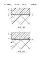
- FIG. 3Adepicts a stiff-surfaced elastomeric dielectric positioned adjacent an interface in accordance with one embodiment of the invention.
- FIG. 3Bdepicts a stiff-surfaced, microstructured elastomeric dielectric positioned adjacent an interface in accordance with a further embodiment of the invention.
- FIG. 3Cis similar to FIG. 3B and shows a pair of electrodes for controllably deforming the microstructured elastomeric dielectric toward the adjacent interface.
- FIG. 4is a graph on which percentage reflectivity is plotted as a function of pressure applied between the elastomeric dielectric and the interface of FIG. 3.
- FIG. 5is a flowchart illustrating a stiffening method in accordance with the invention.
- FIG. 3Adepicts an elastomeric dielectric 10 positioned adjacent interface 12.
- Light rays 14 incident upon interface 12are totally internally reflected because air gap 16 between the opposing surfaces of dielectric 10 and interface 12 is large enough to prevent optical contact between the opposing surfaces (i.e. gap 16 is substantially greater than one micron).
- the Young's Modulus E of dielectric 10varies as a function of distance from the surface of dielectric 10 adjacent interface 12, such that the portion 18 of dielectric 10 near the surface is substantially stiffer than in the remaining portions of dielectric 10.
- the stiffened surface portion 18 of dielectric 10prevents attainment of the aforementioned Van der Waals bonding between dielectric 10 and interface 12, since such bonding occurs only if dielectric 10 is sufficiently deformable.
- the Young's Modulus of a material(a measure of the material's stiffness) must be less than the Van der Waals bond energy per unit area divided by a characteristic dimension associated with the material's surface roughness, in order for substantial atomic contact to occur.
- the Young's Modulusis less than about 10 6 Pascals, which is the case for elastomeric materials.
- the aforementioned surface stiffeningshould be such that the surface of dielectric 10 can assist in achieving a predictable, reproducible degree of frustration of total internal reflection which varies as function of the pressure applied between dielectric 10 and interface 12.
- the surface of dielectric 10can assist in achieving a predictable, reproducible degree of frustration of total internal reflection which varies as function of the pressure applied between dielectric 10 and interface 12.
- air gap 16retains a well defined average value of slightly over one micron. This is important, particularly if the interfacial pressure is to be created by electrostatic force, as such narrow air gaps can support large fields due to the "Paschen effect", and these large fields can be produced with fairly low voltages, due to the small gap.
- One method of creating the desired surface characteristics in elastomeric dielectric 10is to prepare a uniform, smooth-surfaced elastomeric material, and then treat that material in a manner which stiffens and/or textures a thin surface portion of the material.
- One acceptable techniqueis to irradiate the surface of a silicone elastomer with ultraviolet light.
- the inventorsnote that such irradiation is typically performed in the presence of oxygen, so it may be that the combination of the ultraviolet light and the resultant ozone are important.
- the effectmay be to increase cross-linking of polymer chains near the treated surface of the elastomer material, increasing the Young's Modulus in this region.
- the precise nature of the effect(s) involvedis uncertain.
- FIG. 5Another method (FIG. 5) is to separately apply a thin layer of stiff material to the surface of an elastomeric material. More particularly, a sacrificial microstructured film is coated with a thin non-sticky polymer having a preselected stiffness.
- a sacrificial microstructured filmis coated with a thin non-sticky polymer having a preselected stiffness.
- One way of making such a coatingis to spin cast liquid poly-methyl-methacrylate (“PMMA”) which then polymerizes to yield a sub-micron thick coating; while another way is to vacuum deposit parylene on the film. Elastomer is then cast against the PMMA.
- the sacrificial filmis then dissolved by a solvent which does not attack the coating or the elastomer, leaving the microstructured surface adherent to the elastomeric material.
- FIG. 3Bdepicts such a stiffened microstructured surface 20 bonded to elastomeric dielectric 10.
- FIG. 3Bdepicts a first electrode 22 bonded between stiffened microstructured surface 20 and the remaining flexible portion of dielectric 10; and, a second electrode 24 bonded to interface 12.
- a voltage source "V”is electrically coupled between electrodes 22, 24.
- dielectric 10is preferably a silicone elastomer, it need not necessarily be an "elastomer"; it is sufficient for the bulk dielectric material to be a reasonably flexible substance, such as TeflonTM. Accordingly, the scope of the invention is to be construed in accordance with the substance defined by the following claims.
Landscapes
- Physics & Mathematics (AREA)
- General Physics & Mathematics (AREA)
- Optics & Photonics (AREA)
- Health & Medical Sciences (AREA)
- Toxicology (AREA)
- Engineering & Computer Science (AREA)
- Plasma & Fusion (AREA)
- Laminated Bodies (AREA)
- Mechanical Light Control Or Optical Switches (AREA)
- Manufacture Of Macromolecular Shaped Articles (AREA)
- Shaping Of Tube Ends By Bending Or Straightening (AREA)
Abstract
Description
Claims (1)
Priority Applications (10)
| Application Number | Priority Date | Filing Date | Title |
|---|---|---|---|
| US08/923,431US5999307A (en) | 1997-09-04 | 1997-09-04 | Method and apparatus for controllable frustration of total internal reflection |
| CN98808874ACN1269891A (en) | 1997-09-04 | 1998-05-08 | Method and apparatus for controllable frustration of total internal reflection |
| AU73289/98AAU7328998A (en) | 1997-09-04 | 1998-05-08 | Method and apparatus for controllable frustration of total internal reflection |
| KR1020007001887AKR20010023255A (en) | 1997-09-04 | 1998-05-08 | Method and apparatus for controllable frustration of total internal reflection |
| CA002301289ACA2301289A1 (en) | 1997-09-04 | 1998-05-08 | Method and apparatus for controllable frustration of total internal reflection |
| PCT/CA1998/000457WO1999012069A1 (en) | 1997-09-04 | 1998-05-08 | Method and apparatus for controllable frustration of total internal reflection |
| EP98920429AEP1015932A1 (en) | 1997-09-04 | 1998-05-08 | Method and apparatus for controllable frustration of total internal reflection |
| JP2000509011AJP2001515224A (en) | 1997-09-04 | 1998-05-08 | Method and apparatus for controllable attenuation of total internal reflection |
| US09/449,756US6377383B1 (en) | 1997-09-04 | 1999-11-26 | Optical switching by controllable frustration of total internal reflection |
| US10/067,736US6574025B2 (en) | 1997-09-04 | 2002-02-08 | Optical switching by controllable frustration of total internal reflection |
Applications Claiming Priority (1)
| Application Number | Priority Date | Filing Date | Title |
|---|---|---|---|
| US08/923,431US5999307A (en) | 1997-09-04 | 1997-09-04 | Method and apparatus for controllable frustration of total internal reflection |
Related Child Applications (1)
| Application Number | Title | Priority Date | Filing Date |
|---|---|---|---|
| US09/449,756Continuation-In-PartUS6377383B1 (en) | 1997-09-04 | 1999-11-26 | Optical switching by controllable frustration of total internal reflection |
Publications (1)
| Publication Number | Publication Date |
|---|---|
| US5999307Atrue US5999307A (en) | 1999-12-07 |
Family
ID=25448681
Family Applications (1)
| Application Number | Title | Priority Date | Filing Date |
|---|---|---|---|
| US08/923,431Expired - LifetimeUS5999307A (en) | 1997-09-04 | 1997-09-04 | Method and apparatus for controllable frustration of total internal reflection |
Country Status (8)
| Country | Link |
|---|---|
| US (1) | US5999307A (en) |
| EP (1) | EP1015932A1 (en) |
| JP (1) | JP2001515224A (en) |
| KR (1) | KR20010023255A (en) |
| CN (1) | CN1269891A (en) |
| AU (1) | AU7328998A (en) |
| CA (1) | CA2301289A1 (en) |
| WO (1) | WO1999012069A1 (en) |
Cited By (78)
| Publication number | Priority date | Publication date | Assignee | Title |
|---|---|---|---|---|
| US20020021827A1 (en)* | 2000-08-18 | 2002-02-21 | Cross Match Technologies, Inc. | Fingerprint scanner auto-capture system and method |
| US6356679B1 (en) | 2000-03-30 | 2002-03-12 | K2 Optronics, Inc. | Optical routing element for use in fiber optic systems |
| US6384979B1 (en) | 2000-11-30 | 2002-05-07 | The University Of British Columbia | Color filtering and absorbing total internal reflection image display |
| US6433911B1 (en)* | 2000-05-19 | 2002-08-13 | Massachusetts Institute Of Technology | Frustrated total internal reflection-based micro-opto-electro-mechanical modulator/demodulator |
| US6437921B1 (en) | 2001-08-14 | 2002-08-20 | The University Of British Columbia | Total internal reflection prismatically interleaved reflective film display screen |
| US6452734B1 (en) | 2001-11-30 | 2002-09-17 | The University Of British Columbia | Composite electrophoretically-switchable retro-reflective image display |
| US6463192B1 (en) | 2001-02-26 | 2002-10-08 | K2 Optronics, Inc. | Non-blocking micro-optic switch matrix for use in fiber optic systems |
| US6480268B1 (en)* | 2000-02-11 | 2002-11-12 | Optikos Corporation | Method for temporary suppression of reflection for optical measurement |
| US20030016427A1 (en)* | 2001-04-26 | 2003-01-23 | Arnold Joe F. | Silicon rubber surfaces for biometric print TIR prisms |
| US20030038755A1 (en)* | 2001-08-16 | 2003-02-27 | E Ink Corporation | Light modulation by frustration of total internal reflection |
| US6574025B2 (en) | 1997-09-04 | 2003-06-03 | The University Of British Columbia | Optical switching by controllable frustration of total internal reflection |
| US20030214997A1 (en)* | 2002-04-03 | 2003-11-20 | Diekmann Timothy J. | Time or time-temperature indicating articles |
| US6741523B1 (en) | 2000-05-15 | 2004-05-25 | 3M Innovative Properties Company | Microstructured time dependent indicators |
| US6748132B1 (en) | 2001-02-26 | 2004-06-08 | K2 Optronics, Inc. | Wavelength add drop element for configurable add drop multiplexing |
| US20040112750A1 (en)* | 2002-09-03 | 2004-06-17 | E Ink Corporation | Electrophoretic medium with gaseous suspending fluid |
| US20040136047A1 (en)* | 2002-07-30 | 2004-07-15 | The University Of British Columbia | Self-stabilized electrophoretically frustrated total internal reflection display |
| US20040174584A1 (en)* | 2002-03-04 | 2004-09-09 | The University Of British Columbia | Wide viewing angle reflective display |
| US6867850B2 (en) | 2002-01-17 | 2005-03-15 | Cross Match Technologies, Inc. | Light wedge for illuminating a platen in a print scanner |
| US6922276B2 (en) | 2002-12-23 | 2005-07-26 | E Ink Corporation | Flexible electro-optic displays |
| US6928195B2 (en) | 2000-12-18 | 2005-08-09 | Cross Match Technologies, Inc. | Palm scanner using a programmable nutating mirror for increased resolution |
| US6944768B2 (en) | 2002-04-19 | 2005-09-13 | Cross Match Technologies, Inc. | System and methods for access control utilizing two factors to control access |
| US6954260B2 (en) | 2002-01-17 | 2005-10-11 | Cross Match Technologies, Inc. | Systems and methods for illuminating a platen in a print scanner |
| US6996259B2 (en) | 2002-08-02 | 2006-02-07 | Cross Match Technologies, Inc. | System and method for counting ridges in a captured print image |
| US20060061559A1 (en)* | 2004-09-17 | 2006-03-23 | Uni-Pixel Displays, Inc. | Enhanced bandwidth data encoding method |
| US7064740B2 (en) | 2001-11-09 | 2006-06-20 | Sharp Laboratories Of America, Inc. | Backlit display with improved dynamic range |
| US7073711B2 (en) | 2002-04-19 | 2006-07-11 | Cross Match Technologies, Inc. | Mobile handheld code reader and print scanner system and method |
| US7079007B2 (en) | 2002-04-19 | 2006-07-18 | Cross Match Technologies, Inc. | Systems and methods utilizing biometric data |
| US7103201B2 (en) | 1998-04-28 | 2006-09-05 | Cross Match Technologies, Inc. | Methods for capturing fingerprint images using a moving platen |
| US20060209418A1 (en)* | 2005-03-16 | 2006-09-21 | The University Of British Columbia | Optically coupled toroidal lens:hemi-bead brightness enhancer for total internal reflection modulated image displays |
| US20060238443A1 (en)* | 2003-11-14 | 2006-10-26 | Uni-Pixel Displays, Inc. | Simple matrix addressing in a display |
| US20060268386A1 (en)* | 2002-02-26 | 2006-11-30 | Uni-Pixel Displays, Inc. | Enhancing a field sequential color palette in an optical display |
| US7164440B2 (en) | 2003-02-28 | 2007-01-16 | Cross Match Technologies, Inc. | Dynamic image adaptation method for adjusting the quality of digital prints |
| US7164284B2 (en) | 2003-12-18 | 2007-01-16 | Sharp Laboratories Of America, Inc. | Dynamic gamma for a liquid crystal display |
| US20070047051A1 (en)* | 2005-08-30 | 2007-03-01 | Uni-Pixel Displays, Inc. | Electromechanical dynamic force profile articulating mechanism |
| US20070047887A1 (en)* | 2005-08-30 | 2007-03-01 | Uni-Pixel Displays, Inc. | Reducing light leakage and improving contrast ratio performance in FTIR display devices |
| US7203344B2 (en) | 2002-01-17 | 2007-04-10 | Cross Match Technologies, Inc. | Biometric imaging system and method |
| US20070091011A1 (en)* | 2003-10-03 | 2007-04-26 | Uni-Pixel Displays, Inc. | Z-Axis Redundant Display / Multilayer Display |
| US7277562B2 (en) | 2003-08-01 | 2007-10-02 | Cross Match Technologies, Inc. | Biometric imaging capture system and method |
| US20070242334A1 (en)* | 2006-01-24 | 2007-10-18 | Uni-Pixel Displays, Inc. | Corner-Cube Retroreflectors for Displays |
| US7342592B2 (en) | 2004-06-14 | 2008-03-11 | Sharp Laboratories Of America, Inc. | System for reducing crosstalk |
| US20080192065A1 (en)* | 2005-08-02 | 2008-08-14 | Uni-Pixel Displays, Inc. | Mechanism to Mitigate Color Breakup Artifacts in Field Sequential Color Display Systems |
| US20080289710A1 (en)* | 1999-06-28 | 2008-11-27 | California Institute Of Technology | Microfabricated elastomeric valve and pump systems |
| US7505018B2 (en) | 2004-05-04 | 2009-03-17 | Sharp Laboratories Of America, Inc. | Liquid crystal display with reduced black level insertion |
| US7525528B2 (en) | 2004-11-16 | 2009-04-28 | Sharp Laboratories Of America, Inc. | Technique that preserves specular highlights |
| US7532192B2 (en) | 2004-05-04 | 2009-05-12 | Sharp Laboratories Of America, Inc. | Liquid crystal display with filtered black point |
| US20090142020A1 (en)* | 2006-01-24 | 2009-06-04 | Uni-Pixel Displays, Inc. | Optical microstructures for light extraction and control |
| US7556836B2 (en) | 2004-09-03 | 2009-07-07 | Solae, Llc | High protein snack product |
| US7592996B2 (en) | 2006-06-02 | 2009-09-22 | Samsung Electronics Co., Ltd. | Multiprimary color display with dynamic gamut mapping |
| US7602369B2 (en) | 2004-05-04 | 2009-10-13 | Sharp Laboratories Of America, Inc. | Liquid crystal display with colored backlight |
| US20090262414A1 (en)* | 2006-04-19 | 2009-10-22 | The University Of British Columbia | Ionic electrophoresis in tir-modulated reflective image displays |
| US7612757B2 (en) | 2004-05-04 | 2009-11-03 | Sharp Laboratories Of America, Inc. | Liquid crystal display with modulated black point |
| US7623105B2 (en) | 2003-11-21 | 2009-11-24 | Sharp Laboratories Of America, Inc. | Liquid crystal display with adaptive color |
| US20100085627A1 (en)* | 2006-01-17 | 2010-04-08 | The University Of British Columbia | Microlens-assisted brightness enhancement in reflective image displays |
| US7777714B2 (en) | 2004-05-04 | 2010-08-17 | Sharp Laboratories Of America, Inc. | Liquid crystal display with adaptive width |
| US7853094B2 (en) | 2006-01-24 | 2010-12-14 | Sharp Laboratories Of America, Inc. | Color enhancement technique using skin color detection |
| US7872631B2 (en) | 2004-05-04 | 2011-01-18 | Sharp Laboratories Of America, Inc. | Liquid crystal display with temporal black point |
| US7898519B2 (en) | 2005-02-17 | 2011-03-01 | Sharp Laboratories Of America, Inc. | Method for overdriving a backlit display |
| US8002933B2 (en)* | 1999-06-28 | 2011-08-23 | California Institute Of Technology | Microfabricated elastomeric valve and pump systems |
| US8050512B2 (en) | 2004-11-16 | 2011-11-01 | Sharp Laboratories Of America, Inc. | High dynamic range images from low dynamic range images |
| US8050511B2 (en) | 2004-11-16 | 2011-11-01 | Sharp Laboratories Of America, Inc. | High dynamic range images from low dynamic range images |
| US8104497B2 (en) | 1999-06-28 | 2012-01-31 | California Institute Of Technology | Microfabricated elastomeric valve and pump systems |
| US8121401B2 (en) | 2006-01-24 | 2012-02-21 | Sharp Labortories of America, Inc. | Method for reducing enhancement of artifacts and noise in image color enhancement |
| US8124218B2 (en) | 1999-06-28 | 2012-02-28 | California Institute Of Technology | Microfabricated elastomeric valve and pump systems |
| US8395577B2 (en) | 2004-05-04 | 2013-03-12 | Sharp Laboratories Of America, Inc. | Liquid crystal display with illumination control |
| WO2014160552A1 (en) | 2013-03-26 | 2014-10-02 | Clearink Displays Llc | Displaced porous electrode for frustrating tir |
| US8941580B2 (en) | 2006-11-30 | 2015-01-27 | Sharp Laboratories Of America, Inc. | Liquid crystal display with area adaptive backlight |
| US9280029B2 (en) | 2013-05-13 | 2016-03-08 | Clearink Displays, Inc. | Registered reflective element for a brightness enhanced TIR display |
| US9612501B2 (en) | 2013-09-30 | 2017-04-04 | Clearink Displays, Inc. | Method and apparatus for front-lit semi-retro-reflective display |
| US9740075B2 (en) | 2013-09-10 | 2017-08-22 | Clearink Displays, Inc. | Method and system for perforated reflective film display device |
| US9897890B2 (en) | 2014-10-07 | 2018-02-20 | Clearink Displays, Inc. | Reflective image display with threshold |
| US9939707B2 (en) | 2013-07-08 | 2018-04-10 | Clearink Displays, Inc. | TIR-modulated wide viewing angle display |
| US10203436B2 (en) | 2013-05-22 | 2019-02-12 | Clearink Displays, Inc. | Method and apparatus for improved color filter saturation |
| US10261221B2 (en) | 2015-12-06 | 2019-04-16 | Clearink Displays, Inc. | Corner reflector reflective image display |
| US10304394B2 (en) | 2014-10-08 | 2019-05-28 | Clearink Displays, Inc. | Color filter registered reflective display |
| US10386691B2 (en) | 2015-06-24 | 2019-08-20 | CLEARink Display, Inc. | Method and apparatus for a dry particle totally internally reflective image display |
| US10386547B2 (en) | 2015-12-06 | 2019-08-20 | Clearink Displays, Inc. | Textured high refractive index surface for reflective image displays |
| US10705404B2 (en) | 2013-07-08 | 2020-07-07 | Concord (Hk) International Education Limited | TIR-modulated wide viewing angle display |
| US11650422B2 (en) | 2017-10-23 | 2023-05-16 | Vuzix Corporation | Active correction of aberrations in optical systems |
Families Citing this family (3)
| Publication number | Priority date | Publication date | Assignee | Title |
|---|---|---|---|---|
| WO2011125102A1 (en)* | 2010-04-02 | 2011-10-13 | 株式会社 東芝 | Display device |
| EP2582809A1 (en) | 2010-06-17 | 2013-04-24 | DuPont Nutrition Biosciences ApS | Process |
| DE102011117389B4 (en)* | 2011-10-28 | 2020-01-30 | Schölly Fiberoptic GmbH | endoscope |
Citations (33)
| Publication number | Priority date | Publication date | Assignee | Title |
|---|---|---|---|---|
| US3291554A (en)* | 1963-02-19 | 1966-12-13 | Edgar E Price | Optical neutral controllable density filter |
| US3556638A (en)* | 1968-06-05 | 1971-01-19 | Ibm | Deflector plate for light deflector |
| US3571511A (en)* | 1968-10-25 | 1971-03-16 | Hughes Aircraft Co | Drosograph display system |
| US3698793A (en)* | 1971-03-11 | 1972-10-17 | Kollsman Instr Corp | Solid state display |
| US3746785A (en)* | 1971-11-26 | 1973-07-17 | Bendix Corp | Deflectable membrane optical modulator |
| US3796480A (en)* | 1968-12-26 | 1974-03-12 | Perkin Elmer Corp | Membrane light modulator |
| US4135960A (en)* | 1975-07-21 | 1979-01-23 | American Can Company | Total image transfer process |
| JPS5457576A (en)* | 1977-10-17 | 1979-05-09 | Hayakawa Rubber | Property modifing method of vulcanized rubber product surface |
| US4156745A (en)* | 1978-04-03 | 1979-05-29 | International Business Machines Corporation | Electron sensitive resist and a method preparing the same |
| US4165155A (en)* | 1978-03-27 | 1979-08-21 | International Business Machines Corporation | Amplitude modulation of light beam |
| US4249814A (en)* | 1979-10-01 | 1981-02-10 | Iowa State University Research Foundation, Inc. | Frustrated total internal reflection camera shutter |
| US4324456A (en)* | 1979-08-02 | 1982-04-13 | U.S. Philips Corporation | Electrophoretic projection display systems |
| JPS5978816A (en)* | 1982-10-28 | 1984-05-07 | Showa Electric Wire & Cable Co Ltd | Preparation of synthetic resin film |
| US4448622A (en)* | 1982-04-26 | 1984-05-15 | The United States Of America As Represented By The United States Department Of Energy | Composite polymeric film and method for its use in installing a very thin polymeric film in a device |
| JPS6038130A (en)* | 1983-08-11 | 1985-02-27 | Asahi Chem Ind Co Ltd | Method for manufacturing a polymer thin film adhesively fixed to a frame |
| EP0204427A2 (en)* | 1985-05-02 | 1986-12-10 | RAYCHEM CORPORATION (a Delaware corporation) | Organopolysiloxane materials having decreased surface tack |
| US4714326A (en)* | 1984-03-05 | 1987-12-22 | Canon Kabushiki Kaisha | Method and element for optical modulation |
| DE3720861A1 (en)* | 1987-06-24 | 1989-03-16 | Continental Ag | Process for reducing the surface tackiness of vulcanisable rubber articles |
| US5045847A (en)* | 1988-01-19 | 1991-09-03 | Sanyo Electric Co., Ltd. | Flat display panel |
| US5147519A (en)* | 1990-07-27 | 1992-09-15 | Motorola, Inc. | Method of manufacturing elastomers containing fine line conductors |
| US5221987A (en)* | 1992-04-10 | 1993-06-22 | Laughlin Richard H | FTIR modulator |
| US5235463A (en)* | 1990-12-04 | 1993-08-10 | Thomson-Csf | Method for the making of microlenses for optical applications |
| GB2265024A (en)* | 1992-03-14 | 1993-09-15 | British Aerospace | A spatial light modulator assembly. |
| US5301009A (en)* | 1983-04-28 | 1994-04-05 | The United States Of America As Represented By The Secretary Of The Army | Frustrated total internal reflection optical power limiter |
| US5319491A (en)* | 1990-08-10 | 1994-06-07 | Continental Typographics, Inc. | Optical display |
| US5425710A (en)* | 1993-10-26 | 1995-06-20 | Medtronic, Inc. | Coated sleeve for wrapping dilatation catheter balloons |
| US5455709A (en)* | 1993-03-23 | 1995-10-03 | Martin Marietta Corporation | Total internal reflection spatial light modulation apparatus and method of fabrication thereof |
| EP0728799A1 (en)* | 1995-02-22 | 1996-08-28 | Dow Corning Toray Silicone Co., Ltd. | Method for curing ultraviolet-curable silicone compositions |
| US5555327A (en)* | 1995-06-07 | 1996-09-10 | Laughlin; Richard H. | Frustrated total internal reflection device |
| US5555558A (en)* | 1994-05-27 | 1996-09-10 | Laughlin; Richard H. | Method for switching optical signals |
| US5561541A (en)* | 1984-09-05 | 1996-10-01 | The United States Of America As Represented By The Secretary Of The Army | Frustrated total internal reflection optical power limiter |
| EP0797127A2 (en)* | 1996-03-19 | 1997-09-24 | Shin-Etsu Polymer Co., Ltd. | Semiconductive silicone rubber roller and method for the preparation thereof |
| US5841916A (en)* | 1995-06-07 | 1998-11-24 | Optical Switch Corporation | Frustrated total internal reflection device |
- 1997
- 1997-09-04USUS08/923,431patent/US5999307A/ennot_activeExpired - Lifetime
- 1998
- 1998-05-08CNCN98808874Apatent/CN1269891A/enactivePending
- 1998-05-08EPEP98920429Apatent/EP1015932A1/ennot_activeWithdrawn
- 1998-05-08CACA002301289Apatent/CA2301289A1/ennot_activeAbandoned
- 1998-05-08AUAU73289/98Apatent/AU7328998A/ennot_activeAbandoned
- 1998-05-08WOPCT/CA1998/000457patent/WO1999012069A1/ennot_activeApplication Discontinuation
- 1998-05-08JPJP2000509011Apatent/JP2001515224A/enactivePending
- 1998-05-08KRKR1020007001887Apatent/KR20010023255A/ennot_activeAbandoned
Patent Citations (34)
| Publication number | Priority date | Publication date | Assignee | Title |
|---|---|---|---|---|
| US3291554A (en)* | 1963-02-19 | 1966-12-13 | Edgar E Price | Optical neutral controllable density filter |
| US3556638A (en)* | 1968-06-05 | 1971-01-19 | Ibm | Deflector plate for light deflector |
| US3571511A (en)* | 1968-10-25 | 1971-03-16 | Hughes Aircraft Co | Drosograph display system |
| US3796480A (en)* | 1968-12-26 | 1974-03-12 | Perkin Elmer Corp | Membrane light modulator |
| US3698793A (en)* | 1971-03-11 | 1972-10-17 | Kollsman Instr Corp | Solid state display |
| US3746785A (en)* | 1971-11-26 | 1973-07-17 | Bendix Corp | Deflectable membrane optical modulator |
| US4135960A (en)* | 1975-07-21 | 1979-01-23 | American Can Company | Total image transfer process |
| JPS5457576A (en)* | 1977-10-17 | 1979-05-09 | Hayakawa Rubber | Property modifing method of vulcanized rubber product surface |
| US4165155A (en)* | 1978-03-27 | 1979-08-21 | International Business Machines Corporation | Amplitude modulation of light beam |
| US4156745A (en)* | 1978-04-03 | 1979-05-29 | International Business Machines Corporation | Electron sensitive resist and a method preparing the same |
| US4324456A (en)* | 1979-08-02 | 1982-04-13 | U.S. Philips Corporation | Electrophoretic projection display systems |
| US4249814A (en)* | 1979-10-01 | 1981-02-10 | Iowa State University Research Foundation, Inc. | Frustrated total internal reflection camera shutter |
| US4448622A (en)* | 1982-04-26 | 1984-05-15 | The United States Of America As Represented By The United States Department Of Energy | Composite polymeric film and method for its use in installing a very thin polymeric film in a device |
| JPS5978816A (en)* | 1982-10-28 | 1984-05-07 | Showa Electric Wire & Cable Co Ltd | Preparation of synthetic resin film |
| US5301009A (en)* | 1983-04-28 | 1994-04-05 | The United States Of America As Represented By The Secretary Of The Army | Frustrated total internal reflection optical power limiter |
| JPS6038130A (en)* | 1983-08-11 | 1985-02-27 | Asahi Chem Ind Co Ltd | Method for manufacturing a polymer thin film adhesively fixed to a frame |
| US4714326A (en)* | 1984-03-05 | 1987-12-22 | Canon Kabushiki Kaisha | Method and element for optical modulation |
| US5561541A (en)* | 1984-09-05 | 1996-10-01 | The United States Of America As Represented By The Secretary Of The Army | Frustrated total internal reflection optical power limiter |
| EP0204427A2 (en)* | 1985-05-02 | 1986-12-10 | RAYCHEM CORPORATION (a Delaware corporation) | Organopolysiloxane materials having decreased surface tack |
| DE3720861A1 (en)* | 1987-06-24 | 1989-03-16 | Continental Ag | Process for reducing the surface tackiness of vulcanisable rubber articles |
| US5045847A (en)* | 1988-01-19 | 1991-09-03 | Sanyo Electric Co., Ltd. | Flat display panel |
| US5147519A (en)* | 1990-07-27 | 1992-09-15 | Motorola, Inc. | Method of manufacturing elastomers containing fine line conductors |
| US5319491A (en)* | 1990-08-10 | 1994-06-07 | Continental Typographics, Inc. | Optical display |
| US5235463A (en)* | 1990-12-04 | 1993-08-10 | Thomson-Csf | Method for the making of microlenses for optical applications |
| GB2265024A (en)* | 1992-03-14 | 1993-09-15 | British Aerospace | A spatial light modulator assembly. |
| US5221987A (en)* | 1992-04-10 | 1993-06-22 | Laughlin Richard H | FTIR modulator |
| US5455709A (en)* | 1993-03-23 | 1995-10-03 | Martin Marietta Corporation | Total internal reflection spatial light modulation apparatus and method of fabrication thereof |
| US5425710A (en)* | 1993-10-26 | 1995-06-20 | Medtronic, Inc. | Coated sleeve for wrapping dilatation catheter balloons |
| US5555558A (en)* | 1994-05-27 | 1996-09-10 | Laughlin; Richard H. | Method for switching optical signals |
| US5566260A (en)* | 1994-05-27 | 1996-10-15 | Laughlin; Richard H. | Apparatus for switching optical signals and method of operation |
| EP0728799A1 (en)* | 1995-02-22 | 1996-08-28 | Dow Corning Toray Silicone Co., Ltd. | Method for curing ultraviolet-curable silicone compositions |
| US5555327A (en)* | 1995-06-07 | 1996-09-10 | Laughlin; Richard H. | Frustrated total internal reflection device |
| US5841916A (en)* | 1995-06-07 | 1998-11-24 | Optical Switch Corporation | Frustrated total internal reflection device |
| EP0797127A2 (en)* | 1996-03-19 | 1997-09-24 | Shin-Etsu Polymer Co., Ltd. | Semiconductive silicone rubber roller and method for the preparation thereof |
Non-Patent Citations (8)
| Title |
|---|
| "Elastomeric Light Valves", Qin et al, Advanced Materials 1997, 9, No. 5, pp. 407-410. |
| "Patented fiber switch revs speed, cuts cost", George Kotelly, in "Lightwave" Oct, 1995 Web site publication of PennWell Publishing Co., Tulsa, OK. |
| "Surface Property Changes Induced in Poly(1-Hexene) Elastomer By High Energy Ion Irradition", Carlson et al, Proc. 4th Intl. Conf. on Ion Bean Modification of Materials, Ithaca, NY,Jul. 16-20, 1984. pp. 507-512. |
| Elastomeric Light Valves , Qin et al, Advanced Materials 1997, 9, No. 5, pp. 407 410.* |
| Neufeldt, Victoria. Webster s New World Dictionary of American English Third College Edition. Webster s New World, New York, p. 857, Dec. 31, 19 8.* |
| Neufeldt, Victoria. Webster's New World Dictionary of American English Third College Edition. Webster's New World, New York, p. 857, Dec. 31, 19-8. |
| Patented fiber switch revs speed, cuts cost , George Kotelly, in Lightwave Oct, 1995 Web site publication of PennWell Publishing Co., Tulsa, OK.* |
| Surface Property Changes Induced in Poly(1 Hexene) Elastomer By High Energy Ion Irradition , Carlson et al, Proc. 4th Intl. Conf. on Ion Bean Modification of Materials, Ithaca, NY,Jul. 16 20, 1984. pp. 507 512.* |
Cited By (135)
| Publication number | Priority date | Publication date | Assignee | Title |
|---|---|---|---|---|
| US6574025B2 (en) | 1997-09-04 | 2003-06-03 | The University Of British Columbia | Optical switching by controllable frustration of total internal reflection |
| US7103201B2 (en) | 1998-04-28 | 2006-09-05 | Cross Match Technologies, Inc. | Methods for capturing fingerprint images using a moving platen |
| US8002933B2 (en)* | 1999-06-28 | 2011-08-23 | California Institute Of Technology | Microfabricated elastomeric valve and pump systems |
| US20080289710A1 (en)* | 1999-06-28 | 2008-11-27 | California Institute Of Technology | Microfabricated elastomeric valve and pump systems |
| US8550119B2 (en) | 1999-06-28 | 2013-10-08 | California Institute Of Technology | Microfabricated elastomeric valve and pump systems |
| US8220487B2 (en) | 1999-06-28 | 2012-07-17 | California Institute Of Technology | Microfabricated elastomeric valve and pump systems |
| US8695640B2 (en) | 1999-06-28 | 2014-04-15 | California Institute Of Technology | Microfabricated elastomeric valve and pump systems |
| US8846183B2 (en) | 1999-06-28 | 2014-09-30 | California Institute Of Technology | Microfabricated elastomeric valve and pump systems |
| US8104515B2 (en) | 1999-06-28 | 2012-01-31 | California Institute Of Technology | Microfabricated elastomeric valve and pump systems |
| US8124218B2 (en) | 1999-06-28 | 2012-02-28 | California Institute Of Technology | Microfabricated elastomeric valve and pump systems |
| US8104497B2 (en) | 1999-06-28 | 2012-01-31 | California Institute Of Technology | Microfabricated elastomeric valve and pump systems |
| US6480268B1 (en)* | 2000-02-11 | 2002-11-12 | Optikos Corporation | Method for temporary suppression of reflection for optical measurement |
| US6356679B1 (en) | 2000-03-30 | 2002-03-12 | K2 Optronics, Inc. | Optical routing element for use in fiber optic systems |
| US6741523B1 (en) | 2000-05-15 | 2004-05-25 | 3M Innovative Properties Company | Microstructured time dependent indicators |
| US6433911B1 (en)* | 2000-05-19 | 2002-08-13 | Massachusetts Institute Of Technology | Frustrated total internal reflection-based micro-opto-electro-mechanical modulator/demodulator |
| US20020021827A1 (en)* | 2000-08-18 | 2002-02-21 | Cross Match Technologies, Inc. | Fingerprint scanner auto-capture system and method |
| US6983062B2 (en) | 2000-08-18 | 2006-01-03 | Cross Match Technologies, Inc. | Fingerprint scanner auto-capture system and method |
| US7657067B2 (en) | 2000-08-18 | 2010-02-02 | Cross Match Technologies, Inc. | Fingerprint scanner auto-capture system and method |
| WO2002044806A3 (en)* | 2000-11-30 | 2003-10-09 | Univ British Columbia | Color filtering and absorbing total internal reflection image display |
| US6384979B1 (en) | 2000-11-30 | 2002-05-07 | The University Of British Columbia | Color filtering and absorbing total internal reflection image display |
| US6928195B2 (en) | 2000-12-18 | 2005-08-09 | Cross Match Technologies, Inc. | Palm scanner using a programmable nutating mirror for increased resolution |
| US6748132B1 (en) | 2001-02-26 | 2004-06-08 | K2 Optronics, Inc. | Wavelength add drop element for configurable add drop multiplexing |
| US6463192B1 (en) | 2001-02-26 | 2002-10-08 | K2 Optronics, Inc. | Non-blocking micro-optic switch matrix for use in fiber optic systems |
| WO2002088878A3 (en)* | 2001-04-26 | 2003-07-10 | Cross Match Technologies Inc | Silicone rubber surfaces for biometric print tir prisms |
| US7319565B2 (en)* | 2001-04-26 | 2008-01-15 | Cross Match Technologies, Inc. | Silicone rubber surfaces for biometric print TIR prisms |
| US20030016427A1 (en)* | 2001-04-26 | 2003-01-23 | Arnold Joe F. | Silicon rubber surfaces for biometric print TIR prisms |
| US6437921B1 (en) | 2001-08-14 | 2002-08-20 | The University Of British Columbia | Total internal reflection prismatically interleaved reflective film display screen |
| US6819471B2 (en) | 2001-08-16 | 2004-11-16 | E Ink Corporation | Light modulation by frustration of total internal reflection |
| US20030038755A1 (en)* | 2001-08-16 | 2003-02-27 | E Ink Corporation | Light modulation by frustration of total internal reflection |
| US7675500B2 (en) | 2001-11-09 | 2010-03-09 | Sharp Laboratories Of America, Inc. | Liquid crystal display backlight with variable amplitude LED |
| US7505027B2 (en) | 2001-11-09 | 2009-03-17 | Sharp Laboratories Of America, Inc. | Backlit display with improved dynamic range |
| US7573457B2 (en) | 2001-11-09 | 2009-08-11 | Sharp Laboratories Of America, Inc. | Liquid crystal display backlight with scaling |
| US7064740B2 (en) | 2001-11-09 | 2006-06-20 | Sharp Laboratories Of America, Inc. | Backlit display with improved dynamic range |
| US8378955B2 (en) | 2001-11-09 | 2013-02-19 | Sharp Laboratories Of America, Inc. | Liquid crystal display backlight with filtering |
| US7714830B2 (en) | 2001-11-09 | 2010-05-11 | Sharp Laboratories Of America, Inc. | Liquid crystal display backlight with level change |
| US7505028B2 (en) | 2001-11-09 | 2009-03-17 | Sharp Laboratories Of America, Inc. | Backlit display with improved dynamic range |
| US7499017B2 (en) | 2001-11-09 | 2009-03-03 | Sharp Laboratories Of America, Inc. | Backlit display with improved dynamic range |
| US7737936B2 (en) | 2001-11-09 | 2010-06-15 | Sharp Laboratories Of America, Inc. | Liquid crystal display backlight with modulation |
| US6452734B1 (en) | 2001-11-30 | 2002-09-17 | The University Of British Columbia | Composite electrophoretically-switchable retro-reflective image display |
| US6954260B2 (en) | 2002-01-17 | 2005-10-11 | Cross Match Technologies, Inc. | Systems and methods for illuminating a platen in a print scanner |
| US7586591B2 (en) | 2002-01-17 | 2009-09-08 | Cross Match Technologies, Inc. | Light wedge for illuminating a platen in a print scanner |
| US7308122B2 (en) | 2002-01-17 | 2007-12-11 | Cross Match Technologies, Inc. | Biometric imaging system and method |
| US8073209B2 (en) | 2002-01-17 | 2011-12-06 | Cross Match Technologies, Inc | Biometric imaging system and method |
| US20060170906A1 (en)* | 2002-01-17 | 2006-08-03 | Cross Match Technologies, Inc. | Systems and methods for illuminating a platen in a print scanner |
| US7271881B2 (en) | 2002-01-17 | 2007-09-18 | Cross Match Technologies, Inc. | Systems and methods for illuminating a platen in a print scanner |
| US7203344B2 (en) | 2002-01-17 | 2007-04-10 | Cross Match Technologies, Inc. | Biometric imaging system and method |
| US6867850B2 (en) | 2002-01-17 | 2005-03-15 | Cross Match Technologies, Inc. | Light wedge for illuminating a platen in a print scanner |
| US8014057B2 (en) | 2002-02-26 | 2011-09-06 | Rambus Inc. | Extending the gamut color generation in a display |
| US20070150813A1 (en)* | 2002-02-26 | 2007-06-28 | Uni-Pixel Displays, Inc. | Extending the Gamut Color Generation in an Optical Flat Panel Display |
| US20090262129A1 (en)* | 2002-02-26 | 2009-10-22 | Uni-Pixel Displays, Inc. | Extending the gamut color generation in a display |
| US20060268386A1 (en)* | 2002-02-26 | 2006-11-30 | Uni-Pixel Displays, Inc. | Enhancing a field sequential color palette in an optical display |
| US8077376B2 (en) | 2002-02-26 | 2011-12-13 | Rambus Inc. | Visible plus non-visible field sequential color |
| US7522354B2 (en) | 2002-02-26 | 2009-04-21 | Uni-Pixel Displays, Inc. | Enhancing a field sequential color palette in an optical display |
| US7515326B2 (en) | 2002-02-26 | 2009-04-07 | Uni-Pixel Displays, Inc. | Curved screen display mechanism |
| US6885496B2 (en) | 2002-03-04 | 2005-04-26 | The University Of British Columbia | Wide viewing angle reflective display |
| US20040174584A1 (en)* | 2002-03-04 | 2004-09-09 | The University Of British Columbia | Wide viewing angle reflective display |
| US6891658B2 (en) | 2002-03-04 | 2005-05-10 | The University Of British Columbia | Wide viewing angle reflective display |
| US20030214997A1 (en)* | 2002-04-03 | 2003-11-20 | Diekmann Timothy J. | Time or time-temperature indicating articles |
| US6916116B2 (en) | 2002-04-03 | 2005-07-12 | 3M Innovative Properties Company | Time or time-temperature indicating articles |
| US7073711B2 (en) | 2002-04-19 | 2006-07-11 | Cross Match Technologies, Inc. | Mobile handheld code reader and print scanner system and method |
| US7079007B2 (en) | 2002-04-19 | 2006-07-18 | Cross Match Technologies, Inc. | Systems and methods utilizing biometric data |
| US6944768B2 (en) | 2002-04-19 | 2005-09-13 | Cross Match Technologies, Inc. | System and methods for access control utilizing two factors to control access |
| US20040136047A1 (en)* | 2002-07-30 | 2004-07-15 | The University Of British Columbia | Self-stabilized electrophoretically frustrated total internal reflection display |
| US6865011B2 (en) | 2002-07-30 | 2005-03-08 | The University Of British Columbia | Self-stabilized electrophoretically frustrated total internal reflection display |
| US6996259B2 (en) | 2002-08-02 | 2006-02-07 | Cross Match Technologies, Inc. | System and method for counting ridges in a captured print image |
| US20040112750A1 (en)* | 2002-09-03 | 2004-06-17 | E Ink Corporation | Electrophoretic medium with gaseous suspending fluid |
| US8129655B2 (en) | 2002-09-03 | 2012-03-06 | E Ink Corporation | Electrophoretic medium with gaseous suspending fluid |
| US6922276B2 (en) | 2002-12-23 | 2005-07-26 | E Ink Corporation | Flexible electro-optic displays |
| US7164440B2 (en) | 2003-02-28 | 2007-01-16 | Cross Match Technologies, Inc. | Dynamic image adaptation method for adjusting the quality of digital prints |
| US7277562B2 (en) | 2003-08-01 | 2007-10-02 | Cross Match Technologies, Inc. | Biometric imaging capture system and method |
| US7999759B2 (en) | 2003-10-03 | 2011-08-16 | Rambus Inc. | Z-axis redundant display / multilayer display |
| US20070091011A1 (en)* | 2003-10-03 | 2007-04-26 | Uni-Pixel Displays, Inc. | Z-Axis Redundant Display / Multilayer Display |
| US8085260B2 (en) | 2003-11-14 | 2011-12-27 | Rambus, Inc. | Simple matrix addressing in a display |
| US20060238443A1 (en)* | 2003-11-14 | 2006-10-26 | Uni-Pixel Displays, Inc. | Simple matrix addressing in a display |
| US7764281B2 (en) | 2003-11-14 | 2010-07-27 | Rambus International Ltd. | Simple matrix addressing in a display |
| US7623105B2 (en) | 2003-11-21 | 2009-11-24 | Sharp Laboratories Of America, Inc. | Liquid crystal display with adaptive color |
| US7164284B2 (en) | 2003-12-18 | 2007-01-16 | Sharp Laboratories Of America, Inc. | Dynamic gamma for a liquid crystal display |
| US7612757B2 (en) | 2004-05-04 | 2009-11-03 | Sharp Laboratories Of America, Inc. | Liquid crystal display with modulated black point |
| US7532192B2 (en) | 2004-05-04 | 2009-05-12 | Sharp Laboratories Of America, Inc. | Liquid crystal display with filtered black point |
| US7505018B2 (en) | 2004-05-04 | 2009-03-17 | Sharp Laboratories Of America, Inc. | Liquid crystal display with reduced black level insertion |
| US7602369B2 (en) | 2004-05-04 | 2009-10-13 | Sharp Laboratories Of America, Inc. | Liquid crystal display with colored backlight |
| US8400396B2 (en) | 2004-05-04 | 2013-03-19 | Sharp Laboratories Of America, Inc. | Liquid crystal display with modulation for colored backlight |
| US8395577B2 (en) | 2004-05-04 | 2013-03-12 | Sharp Laboratories Of America, Inc. | Liquid crystal display with illumination control |
| US7872631B2 (en) | 2004-05-04 | 2011-01-18 | Sharp Laboratories Of America, Inc. | Liquid crystal display with temporal black point |
| US7777714B2 (en) | 2004-05-04 | 2010-08-17 | Sharp Laboratories Of America, Inc. | Liquid crystal display with adaptive width |
| US7342592B2 (en) | 2004-06-14 | 2008-03-11 | Sharp Laboratories Of America, Inc. | System for reducing crosstalk |
| US7556836B2 (en) | 2004-09-03 | 2009-07-07 | Solae, Llc | High protein snack product |
| US20060061559A1 (en)* | 2004-09-17 | 2006-03-23 | Uni-Pixel Displays, Inc. | Enhanced bandwidth data encoding method |
| US7564874B2 (en) | 2004-09-17 | 2009-07-21 | Uni-Pixel Displays, Inc. | Enhanced bandwidth data encoding method |
| US8050511B2 (en) | 2004-11-16 | 2011-11-01 | Sharp Laboratories Of America, Inc. | High dynamic range images from low dynamic range images |
| US8050512B2 (en) | 2004-11-16 | 2011-11-01 | Sharp Laboratories Of America, Inc. | High dynamic range images from low dynamic range images |
| US7525528B2 (en) | 2004-11-16 | 2009-04-28 | Sharp Laboratories Of America, Inc. | Technique that preserves specular highlights |
| US7898519B2 (en) | 2005-02-17 | 2011-03-01 | Sharp Laboratories Of America, Inc. | Method for overdriving a backlit display |
| US20060209418A1 (en)* | 2005-03-16 | 2006-09-21 | The University Of British Columbia | Optically coupled toroidal lens:hemi-bead brightness enhancer for total internal reflection modulated image displays |
| US7164536B2 (en) | 2005-03-16 | 2007-01-16 | The University Of British Columbia | Optically coupled toroidal lens:hemi-bead brightness enhancer for total internal reflection modulated image displays |
| US20080192065A1 (en)* | 2005-08-02 | 2008-08-14 | Uni-Pixel Displays, Inc. | Mechanism to Mitigate Color Breakup Artifacts in Field Sequential Color Display Systems |
| US8115776B2 (en) | 2005-08-02 | 2012-02-14 | Rambus Inc. | Mechanism to mitigate color breakup artifacts in field sequential color display systems |
| US8509582B2 (en) | 2005-08-30 | 2013-08-13 | Rambus Delaware Llc | Reducing light leakage and improving contrast ratio performance in FTIR display devices |
| US7449759B2 (en) | 2005-08-30 | 2008-11-11 | Uni-Pixel Displays, Inc. | Electromechanical dynamic force profile articulating mechanism |
| US7817332B2 (en) | 2005-08-30 | 2010-10-19 | Rambus International Ltd. | Electromechanical dynamic force profile articulating mechanism |
| US20080212158A1 (en)* | 2005-08-30 | 2008-09-04 | Unipixel Displays, Inc. | Electromechanical dynamic force profile articulating mechanism |
| US7535611B2 (en) | 2005-08-30 | 2009-05-19 | Unipixel Displays, Inc. | Electromechanical dynamic force profile articulating mechanism |
| US20070047887A1 (en)* | 2005-08-30 | 2007-03-01 | Uni-Pixel Displays, Inc. | Reducing light leakage and improving contrast ratio performance in FTIR display devices |
| US20080158637A1 (en)* | 2005-08-30 | 2008-07-03 | Unipixel Displays, Inc. | Electromechanical dynamic force profile articulating mechanism |
| US20070047051A1 (en)* | 2005-08-30 | 2007-03-01 | Uni-Pixel Displays, Inc. | Electromechanical dynamic force profile articulating mechanism |
| US20100085627A1 (en)* | 2006-01-17 | 2010-04-08 | The University Of British Columbia | Microlens-assisted brightness enhancement in reflective image displays |
| US7760417B2 (en) | 2006-01-17 | 2010-07-20 | The University Of British Columbia | Brightness enhancement by fluid interface deformation in TIR-modulated displays |
| US9143657B2 (en) | 2006-01-24 | 2015-09-22 | Sharp Laboratories Of America, Inc. | Color enhancement technique using skin color detection |
| US8121401B2 (en) | 2006-01-24 | 2012-02-21 | Sharp Labortories of America, Inc. | Method for reducing enhancement of artifacts and noise in image color enhancement |
| US8218920B2 (en) | 2006-01-24 | 2012-07-10 | Rambus Inc. | Optical microstructures for light extraction and control |
| US7853094B2 (en) | 2006-01-24 | 2010-12-14 | Sharp Laboratories Of America, Inc. | Color enhancement technique using skin color detection |
| US8380026B2 (en) | 2006-01-24 | 2013-02-19 | Rambus Inc. | Optical microstructures for light extraction and control |
| US20070242334A1 (en)* | 2006-01-24 | 2007-10-18 | Uni-Pixel Displays, Inc. | Corner-Cube Retroreflectors for Displays |
| US7450799B2 (en) | 2006-01-24 | 2008-11-11 | Uni-Pixel Displays, Inc. | Corner-cube retroreflectors for displays |
| US20090142020A1 (en)* | 2006-01-24 | 2009-06-04 | Uni-Pixel Displays, Inc. | Optical microstructures for light extraction and control |
| US20090262414A1 (en)* | 2006-04-19 | 2009-10-22 | The University Of British Columbia | Ionic electrophoresis in tir-modulated reflective image displays |
| US8040591B2 (en) | 2006-04-19 | 2011-10-18 | The University Of British Columbia | Ionic electrophoresis in TIR-modulated reflective image displays |
| US7592996B2 (en) | 2006-06-02 | 2009-09-22 | Samsung Electronics Co., Ltd. | Multiprimary color display with dynamic gamut mapping |
| US8941580B2 (en) | 2006-11-30 | 2015-01-27 | Sharp Laboratories Of America, Inc. | Liquid crystal display with area adaptive backlight |
| WO2014160552A1 (en) | 2013-03-26 | 2014-10-02 | Clearink Displays Llc | Displaced porous electrode for frustrating tir |
| US9939706B2 (en) | 2013-03-26 | 2018-04-10 | Clearink Displays, Inc. | Displaced porous electrode for frustrating TIR and returning light through exit pupil |
| US9746740B2 (en) | 2013-05-13 | 2017-08-29 | Clearink Displays, Inc. | Registered reflective element for a brightness enhanced TIR display |
| US9280029B2 (en) | 2013-05-13 | 2016-03-08 | Clearink Displays, Inc. | Registered reflective element for a brightness enhanced TIR display |
| US10203436B2 (en) | 2013-05-22 | 2019-02-12 | Clearink Displays, Inc. | Method and apparatus for improved color filter saturation |
| US9939707B2 (en) | 2013-07-08 | 2018-04-10 | Clearink Displays, Inc. | TIR-modulated wide viewing angle display |
| EP3327498A1 (en) | 2013-07-08 | 2018-05-30 | Clearink Displays, Inc. | Tir-modulated wide viewing angle display |
| US10705404B2 (en) | 2013-07-08 | 2020-07-07 | Concord (Hk) International Education Limited | TIR-modulated wide viewing angle display |
| US9740075B2 (en) | 2013-09-10 | 2017-08-22 | Clearink Displays, Inc. | Method and system for perforated reflective film display device |
| US9612501B2 (en) | 2013-09-30 | 2017-04-04 | Clearink Displays, Inc. | Method and apparatus for front-lit semi-retro-reflective display |
| US9897890B2 (en) | 2014-10-07 | 2018-02-20 | Clearink Displays, Inc. | Reflective image display with threshold |
| US10304394B2 (en) | 2014-10-08 | 2019-05-28 | Clearink Displays, Inc. | Color filter registered reflective display |
| US10386691B2 (en) | 2015-06-24 | 2019-08-20 | CLEARink Display, Inc. | Method and apparatus for a dry particle totally internally reflective image display |
| US10261221B2 (en) | 2015-12-06 | 2019-04-16 | Clearink Displays, Inc. | Corner reflector reflective image display |
| US10386547B2 (en) | 2015-12-06 | 2019-08-20 | Clearink Displays, Inc. | Textured high refractive index surface for reflective image displays |
| US11650422B2 (en) | 2017-10-23 | 2023-05-16 | Vuzix Corporation | Active correction of aberrations in optical systems |
Also Published As
| Publication number | Publication date |
|---|---|
| WO1999012069A1 (en) | 1999-03-11 |
| CA2301289A1 (en) | 1999-03-11 |
| JP2001515224A (en) | 2001-09-18 |
| KR20010023255A (en) | 2001-03-26 |
| EP1015932A1 (en) | 2000-07-05 |
| AU7328998A (en) | 1999-03-22 |
| CN1269891A (en) | 2000-10-11 |
Similar Documents
| Publication | Publication Date | Title |
|---|---|---|
| US5999307A (en) | Method and apparatus for controllable frustration of total internal reflection | |
| US6377383B1 (en) | Optical switching by controllable frustration of total internal reflection | |
| Silberzan et al. | Study of the self-adhesion hysteresis of a siloxane elastomer using the JKR method | |
| JP4502445B2 (en) | Method for producing antireflection film | |
| JP4444632B2 (en) | Optical film | |
| JP4058256B2 (en) | Anti-reflection film and anti-reflection treated object | |
| JP7389259B2 (en) | Optical film with antifouling layer | |
| JP5884264B2 (en) | Film with surface protection film, polarizing plate and method for producing the same | |
| JP3974219B2 (en) | Gas barrier film | |
| KR102600830B1 (en) | Low-friction film, manufacturing method therefor, molded body, and method for enhancing finger slipperiness | |
| JP2005331607A (en) | Optical component and image display apparatus | |
| JPH1195012A (en) | Light scattering film | |
| JP3592765B2 (en) | Optical functional film and method for producing the same | |
| KR20210154389A (en) | Stretchable transparency-adjusting film having an orientated heterogeneous interface, method for manufacturing the same and smart window having stretchable transparency-adjusting film | |
| JP2002333508A (en) | Manufacturing method of anti-reflective material | |
| JP3749309B2 (en) | Energy ray-curable resin composition and triacetyl cellulose film having a cured film layer of the composition | |
| JP4319880B2 (en) | Antireflection film, antireflection film and image display device | |
| JP6065966B2 (en) | Manufacturing method of polarizing plate | |
| JP2004230562A (en) | Hard coat film | |
| JPH0228267A (en) | Coating composition | |
| JP7092900B2 (en) | Laminates and image display devices | |
| JP2004158253A (en) | Transparent conductive film and touch panel | |
| JP2010055018A (en) | Display medium and method of manufacturing display medium | |
| WO2023014693A1 (en) | Abrasion-resistant composite | |
| JP2002019040A (en) | Protective film for protecting the surface of optical members |
Legal Events
| Date | Code | Title | Description |
|---|---|---|---|
| AS | Assignment | Owner name:UNIVERSITY OF BRITISH COLUMBIA, THE, CANADA Free format text:ASSIGNMENT OF ASSIGNORS INTEREST;ASSIGNORS:WHITEHEAD, LORNE A.;TIEDJE, J. THOMAS;COOPE, ROBIN JOHN NOEL;REEL/FRAME:008796/0094 Effective date:19970903 | |
| STCF | Information on status: patent grant | Free format text:PATENTED CASE | |
| FEPP | Fee payment procedure | Free format text:PAT HOLDER CLAIMS SMALL ENTITY STATUS, ENTITY STATUS SET TO SMALL (ORIGINAL EVENT CODE: LTOS); ENTITY STATUS OF PATENT OWNER: SMALL ENTITY | |
| FPAY | Fee payment | Year of fee payment:4 | |
| REMI | Maintenance fee reminder mailed | ||
| FEPP | Fee payment procedure | Free format text:PAT HOLDER NO LONGER CLAIMS SMALL ENTITY STATUS, ENTITY STATUS SET TO UNDISCOUNTED (ORIGINAL EVENT CODE: STOL); ENTITY STATUS OF PATENT OWNER: SMALL ENTITY | |
| FPAY | Fee payment | Year of fee payment:8 | |
| FEPP | Fee payment procedure | Free format text:PAT HOLDER CLAIMS SMALL ENTITY STATUS, ENTITY STATUS SET TO SMALL (ORIGINAL EVENT CODE: LTOS); ENTITY STATUS OF PATENT OWNER: SMALL ENTITY | |
| FPAY | Fee payment | Year of fee payment:12 | |
| AS | Assignment | Owner name:CLEARINK DISPLAYS LLC, CALIFORNIA Free format text:ASSIGNMENT OF ASSIGNORS INTEREST;ASSIGNOR:UNIVERSITY OF BRITISH COLUMBIA;REEL/FRAME:030031/0760 Effective date:20130131 | |
| AS | Assignment | Owner name:CLEARINK DISPLAYS, INC., CALIFORNIA Free format text:CHANGE OF NAME;ASSIGNOR:CLEARINK DISPLAYS, LLC;REEL/FRAME:038544/0373 Effective date:20151104 | |
| AS | Assignment | Owner name:CLEARINK DISPLAYS, INC., CALIFORNIA Free format text:CHANGE OF ADDRESS;ASSIGNOR:CLEARINK DISPLAYS, INC.;REEL/FRAME:039903/0962 Effective date:20160902 | |
| AS | Assignment | Owner name:CONCORD (HK) INTERNATIONAL EDUCATION LIMITED, HONG KONG Free format text:ASSIGNMENT OF ASSIGNORS INTEREST;ASSIGNOR:CLEARINK DISPLAYS, INC.;REEL/FRAME:052484/0742 Effective date:20200415 |