US5998935A - AC plasma display with dual discharge sites and contrast enhancement bars - Google Patents
AC plasma display with dual discharge sites and contrast enhancement barsDownload PDFInfo
- Publication number
- US5998935A US5998935AUS09/310,553US31055399AUS5998935AUS 5998935 AUS5998935 AUS 5998935AUS 31055399 AUS31055399 AUS 31055399AUS 5998935 AUS5998935 AUS 5998935A
- Authority
- US
- United States
- Prior art keywords
- sustain
- scan
- trace
- pdp
- loop
- Prior art date
- Legal status (The legal status is an assumption and is not a legal conclusion. Google has not performed a legal analysis and makes no representation as to the accuracy of the status listed.)
- Expired - Lifetime
Links
Images


Classifications
- H—ELECTRICITY
- H01—ELECTRIC ELEMENTS
- H01J—ELECTRIC DISCHARGE TUBES OR DISCHARGE LAMPS
- H01J11/00—Gas-filled discharge tubes with alternating current induction of the discharge, e.g. alternating current plasma display panels [AC-PDP]; Gas-filled discharge tubes without any main electrode inside the vessel; Gas-filled discharge tubes with at least one main electrode outside the vessel
- H01J11/20—Constructional details
- H01J11/34—Vessels, containers or parts thereof, e.g. substrates
- H01J11/44—Optical arrangements or shielding arrangements, e.g. filters, black matrices, light reflecting means or electromagnetic shielding means
- G—PHYSICS
- G09—EDUCATION; CRYPTOGRAPHY; DISPLAY; ADVERTISING; SEALS
- G09G—ARRANGEMENTS OR CIRCUITS FOR CONTROL OF INDICATING DEVICES USING STATIC MEANS TO PRESENT VARIABLE INFORMATION
- G09G3/00—Control arrangements or circuits, of interest only in connection with visual indicators other than cathode-ray tubes
- G09G3/20—Control arrangements or circuits, of interest only in connection with visual indicators other than cathode-ray tubes for presentation of an assembly of a number of characters, e.g. a page, by composing the assembly by combination of individual elements arranged in a matrix no fixed position being assigned to or needed to be assigned to the individual characters or partial characters
- G09G3/22—Control arrangements or circuits, of interest only in connection with visual indicators other than cathode-ray tubes for presentation of an assembly of a number of characters, e.g. a page, by composing the assembly by combination of individual elements arranged in a matrix no fixed position being assigned to or needed to be assigned to the individual characters or partial characters using controlled light sources
- G09G3/28—Control arrangements or circuits, of interest only in connection with visual indicators other than cathode-ray tubes for presentation of an assembly of a number of characters, e.g. a page, by composing the assembly by combination of individual elements arranged in a matrix no fixed position being assigned to or needed to be assigned to the individual characters or partial characters using controlled light sources using luminous gas-discharge panels, e.g. plasma panels
- G09G3/288—Control arrangements or circuits, of interest only in connection with visual indicators other than cathode-ray tubes for presentation of an assembly of a number of characters, e.g. a page, by composing the assembly by combination of individual elements arranged in a matrix no fixed position being assigned to or needed to be assigned to the individual characters or partial characters using controlled light sources using luminous gas-discharge panels, e.g. plasma panels using AC panels
- G09G3/298—Control arrangements or circuits, of interest only in connection with visual indicators other than cathode-ray tubes for presentation of an assembly of a number of characters, e.g. a page, by composing the assembly by combination of individual elements arranged in a matrix no fixed position being assigned to or needed to be assigned to the individual characters or partial characters using controlled light sources using luminous gas-discharge panels, e.g. plasma panels using AC panels using surface discharge panels
- G09G3/2983—Control arrangements or circuits, of interest only in connection with visual indicators other than cathode-ray tubes for presentation of an assembly of a number of characters, e.g. a page, by composing the assembly by combination of individual elements arranged in a matrix no fixed position being assigned to or needed to be assigned to the individual characters or partial characters using controlled light sources using luminous gas-discharge panels, e.g. plasma panels using AC panels using surface discharge panels using non-standard pixel electrode arrangements
- H—ELECTRICITY
- H01—ELECTRIC ELEMENTS
- H01J—ELECTRIC DISCHARGE TUBES OR DISCHARGE LAMPS
- H01J11/00—Gas-filled discharge tubes with alternating current induction of the discharge, e.g. alternating current plasma display panels [AC-PDP]; Gas-filled discharge tubes without any main electrode inside the vessel; Gas-filled discharge tubes with at least one main electrode outside the vessel
- H01J11/10—AC-PDPs with at least one main electrode being out of contact with the plasma
- H01J11/12—AC-PDPs with at least one main electrode being out of contact with the plasma with main electrodes provided on both sides of the discharge space
- H—ELECTRICITY
- H01—ELECTRIC ELEMENTS
- H01J—ELECTRIC DISCHARGE TUBES OR DISCHARGE LAMPS
- H01J11/00—Gas-filled discharge tubes with alternating current induction of the discharge, e.g. alternating current plasma display panels [AC-PDP]; Gas-filled discharge tubes without any main electrode inside the vessel; Gas-filled discharge tubes with at least one main electrode outside the vessel
- H01J11/20—Constructional details
- H01J11/22—Electrodes, e.g. special shape, material or configuration
- H01J11/24—Sustain electrodes or scan electrodes
- H—ELECTRICITY
- H01—ELECTRIC ELEMENTS
- H01J—ELECTRIC DISCHARGE TUBES OR DISCHARGE LAMPS
- H01J11/00—Gas-filled discharge tubes with alternating current induction of the discharge, e.g. alternating current plasma display panels [AC-PDP]; Gas-filled discharge tubes without any main electrode inside the vessel; Gas-filled discharge tubes with at least one main electrode outside the vessel
- H01J11/20—Constructional details
- H01J11/34—Vessels, containers or parts thereof, e.g. substrates
- H01J11/38—Dielectric or insulating layers
- H—ELECTRICITY
- H01—ELECTRIC ELEMENTS
- H01J—ELECTRIC DISCHARGE TUBES OR DISCHARGE LAMPS
- H01J11/00—Gas-filled discharge tubes with alternating current induction of the discharge, e.g. alternating current plasma display panels [AC-PDP]; Gas-filled discharge tubes without any main electrode inside the vessel; Gas-filled discharge tubes with at least one main electrode outside the vessel
- H01J11/20—Constructional details
- H01J11/34—Vessels, containers or parts thereof, e.g. substrates
- H01J11/42—Fluorescent layers
- G—PHYSICS
- G09—EDUCATION; CRYPTOGRAPHY; DISPLAY; ADVERTISING; SEALS
- G09G—ARRANGEMENTS OR CIRCUITS FOR CONTROL OF INDICATING DEVICES USING STATIC MEANS TO PRESENT VARIABLE INFORMATION
- G09G2300/00—Aspects of the constitution of display devices
- G09G2300/04—Structural and physical details of display devices
- G09G2300/0439—Pixel structures
- G09G2300/0443—Pixel structures with several sub-pixels for the same colour in a pixel, not specifically used to display gradations
- H—ELECTRICITY
- H01—ELECTRIC ELEMENTS
- H01J—ELECTRIC DISCHARGE TUBES OR DISCHARGE LAMPS
- H01J2211/00—Plasma display panels with alternate current induction of the discharge, e.g. AC-PDPs
- H01J2211/20—Constructional details
- H01J2211/22—Electrodes
- H01J2211/24—Sustain electrodes or scan electrodes
- H01J2211/245—Shape, e.g. cross section or pattern
- H—ELECTRICITY
- H01—ELECTRIC ELEMENTS
- H01J—ELECTRIC DISCHARGE TUBES OR DISCHARGE LAMPS
- H01J2211/00—Plasma display panels with alternate current induction of the discharge, e.g. AC-PDPs
- H01J2211/20—Constructional details
- H01J2211/34—Vessels, containers or parts thereof, e.g. substrates
- H01J2211/44—Optical arrangements or shielding arrangements, e.g. filters or lenses
- H01J2211/444—Means for improving contrast or colour purity, e.g. black matrix or light shielding means
Definitions
- This inventionis related to the front plate electrode design of large area Plasma Display Panels (PDPs) and, more particularly, to an improved large area color AC plasma display panel, which exhibits, improved contrast.
- PDPsPlasma Display Panels
- FIG. 1illustrates a first prior art embodiment of an AC color PDP wherein narrow electrodes are employed on the front panel. More particularly, the AC PDP of FIG. 1 includes a front plate with horizontal plural sustain electrodes 10 that are coupled to a sustain bus 12. A plurality of scan electrodes 14 are juxtaposed to sustain electrodes 10, and both electrode sets are covered by a dielectric layer (not shown). A back plate supports vertical barrier ribs 16 and plural vertical column conductors 18 (shown in phantom). The individual column conductors are covered with red, green or blue phosphors, as the case may be, to enable a full color display to be achieved. The front and rear plates are sealed together and the space therebetween is filled with a dischargeable gas.
- Pixelsare defined by the intersections of (i) an electrode pair comprising a sustain electrode 10 and a juxtaposed scan electrode 14 on the front plate and (ii) three back plate column electrodes 18 for red, green and blue, respectively. Subpixels correspond to individual red, green and blue column electrodes that intersect with the front plate electrode pair.
- Subpixelsare addressed by applying a combination of pulses to both the front sustain electrodes 10 and scan electrodes 14 and one or more selected column electrodes 18. Each addressed subpixel is then discharged continuously (i.e., sustained) by applying pulses only to the front plate electrode pair.
- a PDP utilizing a similar front plate electrode structureis shown in U.S. Pat. No. 4,728,864 to Dick.
- Some PDPshave used wider transparent electrodes that are connected to a high conductivity feed electrode.
- Such an electrode structureis shown in FIG. 2 and includes transparent electrodes 20, which are connected to sustain electrodes 10 and scan electrodes 14, respectively.
- the gap between the electrodesdefines the electrical breakdown characteristic for the PDP.
- the width of the electrodesaffects the pixel capacitance and, therefore, the discharge power requirements.
- the wider transparent electrodes 20provide a means to input greater power levels to the PDP for increased brightness.
- the manufacturing cost of transparent electrodes 20is much greater, due to the increased number of required processing steps.
- the narrow electrode topology of FIG. 1produces a significant amount of light on the outside of the electrodes, virtually eliminating any dark areas between pixel sites.
- sustain electrodes 10 and scan electrodes 14 at the edges of transparent electrodes 20create a shading of the light between the pixel sites, resulting in dark horizontal lines between pixel rows.
- U.S. Pat. No. 4,772,884 to Weber et al.illustrates a further PDP design wherein plasma spreading or "coupling" is employed to couple the plasma at an address cell to one of a plurality of pixels that are adjacent to the addressed cell.
- plasma spreading or "coupling”is employed to couple the plasma at an address cell to one of a plurality of pixels that are adjacent to the addressed cell.
- loop-configured address electrodes and sustain electrodesare employed to enable selective control of plasma coupling.
- a description of other color PDP structures and modes of operationcan be found in "Development of Technologies for Large-Area Color AC Plasma Displays", Shinoda et al., SID 93 Digest, pages 161-164.
- the ambient room contrast ratiois the ratio of the peak white brightness divided by the display's dark level.
- the intensity of the dark levelis a function of the display's background glow plus the ambient light reflecting off the display. For the viewer, a display with a poor ambient room contrast ratio will appear washed out, whereas, in a dark room, the same display will exhibit vibrant colors.
- Ambient room contrasthas traditionally been enhanced by placing a filter in front of the display. Room light is filtered as it comes into the display and is filtered again after it is reflected off the front panel. The panel's active light is likewise filtered, however it only passes through the filter once.
- the transmissivity of commonly used filtersis 50 to 75%. A 50% filter reduces the reflected room light by a factor of 4, but also reduces the display's brightness in half.
- the front filtertypically has an anti-reflective coating to minimize its reflectance.
- the panel's reflectanceis a combination of the reflectivity of the front plate surface, the electrode material's reflectivity, and the phosphor's reflectivity. Of these, the phosphor's reflectivity contributes heavily to the reflectance due to its light color.
- An AC PDP incorporating the inventionincludes a first substrate having plural elongated address electrode structures, with dielectric layers present thereon and including sets of color phosphors.
- a second substrateis opposed to the first substrate and encloses a dischargeable gas therebetween.
- the second substratesupports a plurality of scan electrode structures that are orthogonally oriented to the address electrode structures.
- Each scan electrode structureincludes a scan loop with a first trace and a second trace and a plurality of sustain electrode loops that are interdigitated with the scan electrode loops, each sustain electrode loop including a first trace and a second trace.
- Address circuitryselectively applies address signals to the address electrode structures and scan circuitry applies a scan voltage to the scan electrode loops.
- Gas dischargesoccur at intersections between address electrode structures and both traces of a scan loop to which the scan voltage is applied, so as to create wall charges and dual subpixel sites for each color subpixel. Thereafter, a sustain signal applied to sustain electrode loops causes discharges at each of the dual subpixel sites at which wall charges exist.
- Increased light and resolutionare the result of the dual subpixel discharge sites.
- Electrically isolated contrast enhancement barsare placed within dual discharge site scan and sustain electrode loops and act to block room light from reflecting off the phosphor layer. Accordingly, ambient room contrast ratio of the PDP is enhanced due to the reduced reflection of the room light off the phosphor. Brightness reduction is minimized by the contrast bars being placed in the center of the loops where light is not produced.
- Such a displayexhibiting a contrast ratio improvement, allows use of front filters with higher levels of light transmission, while meeting an ambient room contrast ratio specification. Since the display only has a small reduction of brightness, the overall brightness of the monitor (i.e., PDP and filter) increases significantly. For applications requiring higher contrast ratios, a lower transmission filter may be used in conjunction with the invention. Further improvements may be gained through use of polarized filters and oxidized metallizations.
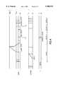
- FIG. 1is a schematic diagram of a prior art color PDP using narrow, scan and sustain electrodes.
- FIG. 2is a schematic diagram of a prior art PDP structure which employs transparent electrodes.
- FIG. 3is a schematic diagram of a PDP that incorporates dual discharge sites.
- FIG. 4is a set of waveform diagrams helpful in understanding the operation of the PDP of FIG. 3
- FIG. 5illustrates a front plate electrode pattern that includes contrast enhancement bars.
- FIG. 6ais a sectional view of the PDP of FIG. 3 that does not include contrast enhancement bars.
- FIG. 6bis a sectional view of a PDP that includes contrast enhancement bars that improve image contrast in ambient light.
- the invention to be described belowbuilds upon the narrow electrode topology shown in FIG. 1, but extends that technology to larger area displays by configuring the narrow electrodes as loops. Such loops enable creation of dual discharge sites at each addressed subpixel, thereby enhancing the brightness and resolution of the resulting display and, further, improving the manufacturability of the PDP.
- a PDP 30which incorporates dual discharge sites, includes a rear panel (not shown) on which column electrodes 32 are positioned. Column electrodes 32 are respectively covered by red, green and blue phosphors. Each column electrode 32 is separated from each other column electrode 32 by a dielectric rib 34, which extends upwardly from the rear plate.
- a transparent front plate(not shown) supports a plurality of sustain loops 36, 38, 40, . . . etc., each sustain loop having an upper trace 36U, 38U, 40U . . . etc. and a lower trace 36L, 38L, 40L . . . etc.
- Each of sustain loops 36, 38 and 40is coupled to a sustain bus 42 which, in turn, is connected to a sustain signal generator 44.
- Scan loops 46, 48, . . . etc.are interdigitated between respective sustain loops 36, 38, 40 . . . etc.
- scan loop 46is positioned between sustain loops 36 and 38
- scan loop 48is positioned between sustain loops 38 and 40.
- Each scan loopincludes an upper trace electrode (46U, 48U) and a lower trace electrode (46L and 48L).
- X address driver 50selectively applies a column drive voltage to one or more column electrodes 32, while scan generator 52 sequentially scans each of scan electrodes 46, 48, etc. Assuming that a subpixel 54 is to be addressed (shown in phantom), X address driver 50 applies a column drive voltage to a column conductor 56.
- scan generator 52applies a row select voltage (FIG. 4) to scan loop 48, a discharge is created between both upper trace electrode 48U, lower trace electrode 48L and column conductor 56. This discharge spreads and discharges the wall capacitances of sustain electrodes 38L and 40U. As a result, a wall charge is established at discharge sites 60 and 62 (substantially immediately below trace electrodes 38L, 48U and 48L, 40U) on the dielectric layers which cover those trace electrodes.
- each addressed subpixelincludes dual discharging sites. To the viewer, discharging subpixel sites 60 and 62 tend to merge and manifest substantial levels of output illumination.
- Dimension Cis the gas discharge gap, which defines the two discharge sites on either side of a scan loop.
- Dimensions A and Dare the inter-electrode distances between the traces of a sustain loop and a scan loop, respectively.
- dimension DIn order to maintain substantially independent discharges at, for example, discharge site 60 and 62, dimension D must be kept large enough to prevent one discharge site from dominating during a discharge action with a column electrode 56. More specifically, if the traces of a scan loop are positioned too close to each other, then two distinct discharge sites are not achieved. In such case, one site will "hog" the discharge and will snuff out the other one, creating discharge voids during subsequent sustain cycles.
- the minimum scan loop dimensionmust be such as to assure substantially independent discharge actions upon application of address and scan potentials to the column electrodes and scan loops, respectively.
- distance Dmay preferably be set to approximately: 0.3 mm.
- dimension Amust be set to exceed a minimum distance so as to prevent a discharge at a subpixel site (e.g., 60) from spreading to a discharge site of an adjacent subpixel (e.g., site 70). If dimension A is made too small, a discharge at site 60 will tend to spread across sustain loop 38 and cause an errant discharge at site 70. This will cause enough wall charge to be removed from site 70 that subsequent discharges will either be too weak or become nonexistent. Accordingly, it is preferred, given a pixel pitch of approximately 1.3 mm, that distance A be approximately 0.4 mm or larger.
- the phosphor on the back plateWith each gas discharge occurring across a gap C, the phosphor on the back plate is excited to produce light which is largely emitted through the discharge gap C. However, a significant amount of light is also emitted from the opposite side of the respective upper and lower traces of the sustain and scan loops. Since light is produced on either side of four electrode traces per pixel, the light is seen as three small bright spots and two dimmer fringing spots. From a distance, the light disturbance caused by the shadowing of the electrodes is negligible and the viewer sees a crisp, clear, high resolution image.
- An added benefit to the structure shown in FIG. 3is that, during processing of the front plate, if a void occurs in one of the loop segments, the remainder of the loop is capable of maintaining the electrical integrity of the entire loop. When processing large plates, this can represent a substantial cost savings.
- FIG. 4a representative set of voltage waveforms is illustrated which enable operation of the PDP shown in FIG. 3.
- an erase pulseis applied to the sustain loops and erases each pixel site on the panel.
- a write pulseis applied by scan generator 52 to all scan loops on the panel to cause a discharge to occur at each subpixel site.
- a high potentialis applied to all sustain loops so that, in combination with a row select pulse applied to the scan loops and an address pulse applied to one or more column electrodes, a selective discharge of addressed subpixel sites is achieved.
- sustain signalsare applied between the scan loops and sustain loops to achieve a continued discharge of the previously selected subpixel sites.
- each addressed subpixelproduces two discharge sites (e.g. 60, 62), one between each side of a scan loop and adjacent sustain loops.
- Light produced from these discharge sitesis largely emitted through discharge gaps C.
- To improve the contrast ratio of such a PDP structureit has been found that positioning of opaque structures between traces of the loop electrodes blocks a substantial amount of reflected ambient light from the phosphor layer while not reducing the emitted light from the PDP by an unacceptable amount.
- FIG. 5shows the same front plate topology as FIG. 3, with opaque structures 100 (hereafter referred to as "contrast enhancement bars") inserted between the traces that comprise each of electrode loops 102.
- Each edge of each contrast enhancement bar 100is positioned a distance E from an adjoining trace of an electrode loop 102 so as not too restrict the strong light emission that occurs inside a respective electrode loop and close to the trace.
- the principal dischargetakes place across the discharge gap (dimension C) between adjacent traces of juxtaposed sustain and scan loops. Accordingly, the principal light emission takes place across the discharge gap, with proportionally smaller light emissions emanating from within the respective loops 102.
- dimension Eis set to be in a range of about 0.5 to 1.0 times the discharge gap C, there is little diminution of emitted discharge light, while there is a substantial increase in ambient light contrast ratio of the PDP.
- FIGS. 6a and 6bshow cross sectional side views of the PDP of FIG. 3, with FIG. 6a illustrating a PDP without the contrast enhancement bars and FIG. 6b with the contrast enhancement bars.
- the PDP structures in both Figuresare identical except for the presence of the contrast enhancement bars 100. Both Figures employ the element numbering found in FIG. 3.
- electrode loop traces 38U, 38L, 48U, 48L, 40U, 40L, etc.reside on front plate 104 and are covered by a dielectric layer 106.
- a filter 108is separated from front plate 104 by an air gap 110.
- a back plate 112supports a column electrode 32 that is covered by a phosphor layer 114.
- a dischargeable gasis present in substrate gap 116.
- Arrows 120, 122 and 124illustrate the light that is given off at a discharge gap C between electrode traces 40U and 48L. As indicated above, most of the emitted discharge light travels along the path of arrow 122, while smaller proportions are emitted along arrows 120 and 124. Note, that there is no structure which blocks ambient light 130 from reflecting off phosphor layer 114 to reduce the contrast ratio of the PDP.
- FIG. 6billustrates the placement of contrast enhancement bars 100 within the respective electrode loops 102 to reduce the amount of ambient light 130 which reaches phosphor layer 114.
- Each edge of each contrast enhancement bar 100is separated by dimension E from an an adjacent loop electrode trace. As dimension E allows a large proportion of the discharge light that is emitted within an electrode loop to pass, only a small part of the discharge light is blocked by a contrast enhancement bar 100 while a large percentage of ambient light is prevented from striking the phosphor.
- contrast enhancement bar 100The addition of a contrast enhancement bar within an electrode loop allows the intense light to be emitted through a discharge gap C and at the inside edges of the loop traces. The scattered light normally emitted from the electrode loop centers is either absorbed or reflected back to phosphor 114 by contrast enhancement bar 100.
- contrast enhancement bars 100The material used for contrast enhancement bars 100 is not critical. For instance, a PDP developed using this technology simply used the same electrode material as the loop electrodes (i.e. chrome/copper/chrome conductors). Such a contrast enhancement bar structure is convenient because it does not require any additional process or alignment steps, only a straightforward electrode mask change. To render the contrast enhancement bar more absorptive, the initial chrome layer deposited on the front panel may be subjected to an oxidation process to blacken its color. Farther, in lieu of a conductive contrast enhancement bar structure, a black glass layer may be screen printed on the front plate and utilized as the contrast enhancement bar structure.
- the conductivity of the contrast enhancement barsis not a hindrance for performance. Since the addressing techniques control the wall charge on the pixel sites very precisely, little charge is placed on the contrast enhancement bars. Furthermore, the contrast enhancement bar is floating, i.e. not connected to the loop electrodes, so there isn't sufficient charge transfer from the loop trace electrode to couple discharges to a contrast enhancement bar. There is also a benefit to be gained from the conductivity of the contrast enhancement bars. During discharge activity, the contrast bars will accumulate a negative charge. Once charged negatively, when the surrounding loop rises in potential to become the anode of a discharge, the negative charge on the contrast enhancement bar is sufficient to repel the spreading discharge which is moving towards the positive voltage. This results in an improvement in cell to cell isolation.
- each contrast enhancement baris semi-reflective and only obstructs scattered light, minimal brightness reduction occurs when the spacing E between the loop trace electrodes and the contrast enhancement bar is in a range of about 0.5 to 1.0 times the discharge gap distance C.
Landscapes
- Engineering & Computer Science (AREA)
- Physics & Mathematics (AREA)
- Plasma & Fusion (AREA)
- Chemical & Material Sciences (AREA)
- Materials Engineering (AREA)
- Power Engineering (AREA)
- Computer Hardware Design (AREA)
- General Physics & Mathematics (AREA)
- Theoretical Computer Science (AREA)
- Electromagnetism (AREA)
- Gas-Filled Discharge Tubes (AREA)
Abstract
Description
Claims (15)
Priority Applications (6)
| Application Number | Priority Date | Filing Date | Title |
|---|---|---|---|
| US09/310,553US5998935A (en) | 1997-09-29 | 1999-05-12 | AC plasma display with dual discharge sites and contrast enhancement bars |
| PCT/GB2000/001833WO2000070644A1 (en) | 1999-05-12 | 2000-05-12 | Ac plasma display with dual discharge sites and contrast enhancement bars |
| KR1020017000474AKR20010104197A (en) | 1999-05-12 | 2000-05-12 | Ac plasma display with dual discharge sites and contrast enhancement bars |
| CNB008008647ACN1299313C (en) | 1999-05-12 | 2000-05-12 | AC Plasma Display with Dual Discharge Dots and Contrast Enhanced Bars |
| JP2000619002AJP2003500797A (en) | 1999-05-12 | 2000-05-12 | AC plasma display with double discharge sites and contrast enhancing bars |
| TW089109011ATW476975B (en) | 1999-05-12 | 2000-08-07 | AC plasma display with dual discharge sites and contrast enhancement bars |
Applications Claiming Priority (2)
| Application Number | Priority Date | Filing Date | Title |
|---|---|---|---|
| US08/939,251US5852347A (en) | 1997-09-29 | 1997-09-29 | Large-area color AC plasma display employing dual discharge sites at each pixel site |
| US09/310,553US5998935A (en) | 1997-09-29 | 1999-05-12 | AC plasma display with dual discharge sites and contrast enhancement bars |
Related Parent Applications (1)
| Application Number | Title | Priority Date | Filing Date |
|---|---|---|---|
| US08/939,251ContinuationUS5852347A (en) | 1997-09-29 | 1997-09-29 | Large-area color AC plasma display employing dual discharge sites at each pixel site |
Publications (1)
| Publication Number | Publication Date |
|---|---|
| US5998935Atrue US5998935A (en) | 1999-12-07 |
Family
ID=23203035
Family Applications (1)
| Application Number | Title | Priority Date | Filing Date |
|---|---|---|---|
| US09/310,553Expired - LifetimeUS5998935A (en) | 1997-09-29 | 1999-05-12 | AC plasma display with dual discharge sites and contrast enhancement bars |
Country Status (6)
| Country | Link |
|---|---|
| US (1) | US5998935A (en) |
| JP (1) | JP2003500797A (en) |
| KR (1) | KR20010104197A (en) |
| CN (1) | CN1299313C (en) |
| TW (1) | TW476975B (en) |
| WO (1) | WO2000070644A1 (en) |
Cited By (21)
| Publication number | Priority date | Publication date | Assignee | Title |
|---|---|---|---|---|
| US6118214A (en)* | 1999-05-12 | 2000-09-12 | Matsushita Electric Industrial Co., Ltd. | AC plasma display with apertured electrode patterns |
| US6144163A (en)* | 1998-07-29 | 2000-11-07 | Pioneer Corporation | Method of driving plasma display device |
| US6411035B1 (en) | 1999-05-12 | 2002-06-25 | Robert G. Marcotte | AC plasma display with apertured electrode patterns |
| US6420830B1 (en)* | 1998-01-26 | 2002-07-16 | Lg Electronics Inc. | Plasma display panel having three discharge sustain electrodes per two pixels |
| US20030062836A1 (en)* | 2001-09-28 | 2003-04-03 | Lg Electronics Inc. | Plasma display panel |
| US6552486B1 (en)* | 1998-11-27 | 2003-04-22 | Matsushita Electric Industrial Co., Ltd. | Plasma display panel with semitransparent front substrate and filter |
| US20030134506A1 (en)* | 2002-01-14 | 2003-07-17 | Plasmion Corporation | Plasma display panel having trench discharge cell and method of fabricating the same |
| US20040001034A1 (en)* | 2002-06-28 | 2004-01-01 | Matsushita Electric Industrial Co., Ltd. | Plasma display with split electrodes |
| US20040212566A1 (en)* | 2002-06-28 | 2004-10-28 | Matsushita Electric Industrial Co., Ltd. | Plasma display with split electrodes |
| US6819307B2 (en)* | 2000-02-03 | 2004-11-16 | Lg Electronics Inc. | Plasma display panel and driving method thereof |
| US20040251808A1 (en)* | 2003-06-10 | 2004-12-16 | Horng-Bin Hsu | Blink plasma backlight system for liquid crystal display |
| US20040263435A1 (en)* | 2003-06-30 | 2004-12-30 | Fujitsu Hitachi Plasma Display Limited | Plasma display device |
| US20050280367A1 (en)* | 2004-06-17 | 2005-12-22 | Joon-Yeon Kim | Plasma display panel and plasma display device |
| US20060129332A1 (en)* | 2004-12-10 | 2006-06-15 | Susumu Mimura | Method and apparatus for measuring physical or chemical phenomena |
| US20060131601A1 (en)* | 2004-12-21 | 2006-06-22 | Ouderkirk Andrew J | Illumination assembly and method of making same |
| US20060131596A1 (en)* | 2004-12-21 | 2006-06-22 | Ouderkirk Andrew J | Illumination assembly and method of making same |
| US20060131602A1 (en)* | 2004-12-21 | 2006-06-22 | Ouderkirk Andrew J | Illumination assembly and method of making same |
| US7125303B2 (en) | 1999-12-09 | 2006-10-24 | Matsushita Electric Industrial Co., Ltd. | Electrode plate and manufacturing method for the same, and gas discharge panel having electrode plate and manufacturing method for the same |
| US7227513B2 (en)* | 1999-11-15 | 2007-06-05 | Lg Electronics Inc | Plasma display and driving method thereof |
| US20100244683A1 (en)* | 2007-10-01 | 2010-09-30 | Hitachi, Ltd. | Plasma display panel |
| US10497335B2 (en)* | 2016-11-21 | 2019-12-03 | Lg Display Co., Ltd. | Display device |
Families Citing this family (2)
| Publication number | Priority date | Publication date | Assignee | Title |
|---|---|---|---|---|
| JP3444875B2 (en) | 1999-12-09 | 2003-09-08 | 松下電器産業株式会社 | Plate with electrodes, method of manufacturing the same, gas discharge panel using the same, and method of manufacturing the same |
| KR100862566B1 (en)* | 2006-08-28 | 2008-10-09 | 엘지전자 주식회사 | Plasma display panel |
Citations (2)
| Publication number | Priority date | Publication date | Assignee | Title |
|---|---|---|---|---|
| US3666981A (en)* | 1969-12-18 | 1972-05-30 | Ibm | Gas cell type memory panel with grid network for electrostatic isolation |
| US4728864A (en)* | 1986-03-03 | 1988-03-01 | American Telephone And Telegraph Company, At&T Bell Laboratories | AC plasma display |
Family Cites Families (7)
| Publication number | Priority date | Publication date | Assignee | Title |
|---|---|---|---|---|
| JP3234270B2 (en)* | 1992-03-19 | 2001-12-04 | 富士通株式会社 | Surface discharge type plasma display panel |
| JPH096281A (en)* | 1995-06-15 | 1997-01-10 | Oki Electric Ind Co Ltd | Plasma display panel driving method and plasma display panel |
| JP3163563B2 (en)* | 1995-08-25 | 2001-05-08 | 富士通株式会社 | Surface discharge type plasma display panel and manufacturing method thereof |
| JPH10144225A (en)* | 1996-11-07 | 1998-05-29 | Noritake Co Ltd | Ac plasma display panel and display device |
| JP3635881B2 (en)* | 1997-08-01 | 2005-04-06 | 松下電器産業株式会社 | Plasma display panel |
| US5852347A (en)* | 1997-09-29 | 1998-12-22 | Matsushita Electric Industries | Large-area color AC plasma display employing dual discharge sites at each pixel site |
| JPH11272232A (en)* | 1998-03-20 | 1999-10-08 | Fujitsu Ltd | Plasma display panel and device using the same |
- 1999
- 1999-05-12USUS09/310,553patent/US5998935A/ennot_activeExpired - Lifetime
- 2000
- 2000-05-12KRKR1020017000474Apatent/KR20010104197A/ennot_activeCeased
- 2000-05-12JPJP2000619002Apatent/JP2003500797A/enactivePending
- 2000-05-12CNCNB008008647Apatent/CN1299313C/ennot_activeExpired - Fee Related
- 2000-05-12WOPCT/GB2000/001833patent/WO2000070644A1/ennot_activeCeased
- 2000-08-07TWTW089109011Apatent/TW476975B/ennot_activeIP Right Cessation
Patent Citations (2)
| Publication number | Priority date | Publication date | Assignee | Title |
|---|---|---|---|---|
| US3666981A (en)* | 1969-12-18 | 1972-05-30 | Ibm | Gas cell type memory panel with grid network for electrostatic isolation |
| US4728864A (en)* | 1986-03-03 | 1988-03-01 | American Telephone And Telegraph Company, At&T Bell Laboratories | AC plasma display |
Non-Patent Citations (2)
| Title |
|---|
| Proc. of Int l Display Workshop, 1998, pp. 575 578, D. I. Kim et al., New AC PDP Structure with Floating Electrodes .* |
| Proc. of Int'l Display Workshop, 1998, pp. 575-578, D. I. Kim et al., "New AC-PDP Structure with Floating Electrodes". |
Cited By (34)
| Publication number | Priority date | Publication date | Assignee | Title |
|---|---|---|---|---|
| US6420830B1 (en)* | 1998-01-26 | 2002-07-16 | Lg Electronics Inc. | Plasma display panel having three discharge sustain electrodes per two pixels |
| US6144163A (en)* | 1998-07-29 | 2000-11-07 | Pioneer Corporation | Method of driving plasma display device |
| US6552486B1 (en)* | 1998-11-27 | 2003-04-22 | Matsushita Electric Industrial Co., Ltd. | Plasma display panel with semitransparent front substrate and filter |
| US6118214A (en)* | 1999-05-12 | 2000-09-12 | Matsushita Electric Industrial Co., Ltd. | AC plasma display with apertured electrode patterns |
| US6411035B1 (en) | 1999-05-12 | 2002-06-25 | Robert G. Marcotte | AC plasma display with apertured electrode patterns |
| US7227513B2 (en)* | 1999-11-15 | 2007-06-05 | Lg Electronics Inc | Plasma display and driving method thereof |
| US7125303B2 (en) | 1999-12-09 | 2006-10-24 | Matsushita Electric Industrial Co., Ltd. | Electrode plate and manufacturing method for the same, and gas discharge panel having electrode plate and manufacturing method for the same |
| US6819307B2 (en)* | 2000-02-03 | 2004-11-16 | Lg Electronics Inc. | Plasma display panel and driving method thereof |
| US20030062836A1 (en)* | 2001-09-28 | 2003-04-03 | Lg Electronics Inc. | Plasma display panel |
| US6768262B2 (en)* | 2001-09-28 | 2004-07-27 | Lg Electronics Inc. | Plasma display panel |
| US20030134506A1 (en)* | 2002-01-14 | 2003-07-17 | Plasmion Corporation | Plasma display panel having trench discharge cell and method of fabricating the same |
| US6897564B2 (en) | 2002-01-14 | 2005-05-24 | Plasmion Displays, Llc. | Plasma display panel having trench discharge cells with one or more electrodes formed therein and extended to outside of the trench |
| US7330166B2 (en) | 2002-06-28 | 2008-02-12 | Matsushita Electronic Industrial Co., Ltd | Plasma display with split electrodes |
| US20040212566A1 (en)* | 2002-06-28 | 2004-10-28 | Matsushita Electric Industrial Co., Ltd. | Plasma display with split electrodes |
| US6853144B2 (en)* | 2002-06-28 | 2005-02-08 | Matsushita Electric Industrial Co., Ltd | Plasma display with split electrodes |
| US20050088377A1 (en)* | 2002-06-28 | 2005-04-28 | Matsushita Electric Industrial Co., Ltd. | Plasma display with split electrodes |
| US20040001034A1 (en)* | 2002-06-28 | 2004-01-01 | Matsushita Electric Industrial Co., Ltd. | Plasma display with split electrodes |
| US7323822B2 (en) | 2002-06-28 | 2008-01-29 | Matsushita Electric Industrial Co., Ltd. | Plasma display with split electrodes |
| US20040251808A1 (en)* | 2003-06-10 | 2004-12-16 | Horng-Bin Hsu | Blink plasma backlight system for liquid crystal display |
| US7157846B2 (en)* | 2003-06-10 | 2007-01-02 | Au Optronics Corporation | Blink plasma backlight system for liquid crystal display |
| US7379032B2 (en)* | 2003-06-30 | 2008-05-27 | Fujitsu Hitachi Plasma Display Limited | Plasma display device |
| US20040263435A1 (en)* | 2003-06-30 | 2004-12-30 | Fujitsu Hitachi Plasma Display Limited | Plasma display device |
| US20050280367A1 (en)* | 2004-06-17 | 2005-12-22 | Joon-Yeon Kim | Plasma display panel and plasma display device |
| US7312574B2 (en)* | 2004-06-17 | 2007-12-25 | Samsung Sdi Co., Ltd. | Plasma display panel having display electrode terminals located on the same side, and plasma display device incorporating the same |
| US20060129332A1 (en)* | 2004-12-10 | 2006-06-15 | Susumu Mimura | Method and apparatus for measuring physical or chemical phenomena |
| US7424372B2 (en) | 2004-12-10 | 2008-09-09 | Horiba, Ltd. | Method and apparatus for measuring physical or chemical phenomena |
| US20060131602A1 (en)* | 2004-12-21 | 2006-06-22 | Ouderkirk Andrew J | Illumination assembly and method of making same |
| US7285802B2 (en) | 2004-12-21 | 2007-10-23 | 3M Innovative Properties Company | Illumination assembly and method of making same |
| US7296916B2 (en) | 2004-12-21 | 2007-11-20 | 3M Innovative Properties Company | Illumination assembly and method of making same |
| US20060131596A1 (en)* | 2004-12-21 | 2006-06-22 | Ouderkirk Andrew J | Illumination assembly and method of making same |
| US20060131601A1 (en)* | 2004-12-21 | 2006-06-22 | Ouderkirk Andrew J | Illumination assembly and method of making same |
| US20100244683A1 (en)* | 2007-10-01 | 2010-09-30 | Hitachi, Ltd. | Plasma display panel |
| US8410694B2 (en)* | 2007-10-01 | 2013-04-02 | Hitachi, Ltd. | Plasma display panel |
| US10497335B2 (en)* | 2016-11-21 | 2019-12-03 | Lg Display Co., Ltd. | Display device |
Also Published As
| Publication number | Publication date |
|---|---|
| CN1299313C (en) | 2007-02-07 |
| CN1304540A (en) | 2001-07-18 |
| KR20010104197A (en) | 2001-11-24 |
| TW476975B (en) | 2002-02-21 |
| JP2003500797A (en) | 2003-01-07 |
| WO2000070644A1 (en) | 2000-11-23 |
Similar Documents
| Publication | Publication Date | Title |
|---|---|---|
| US5998935A (en) | AC plasma display with dual discharge sites and contrast enhancement bars | |
| EP1019892B1 (en) | Large-area colour ac plasma display | |
| US6534914B2 (en) | Plasma display panel | |
| KR20000067805A (en) | Plasma display panel and driving method thereof | |
| KR19990023139A (en) | Electrode Structure of AC Plasma Display Panel | |
| JP2002075214A (en) | Plasma display panel | |
| JP2003203571A (en) | Plasma display panel | |
| JP3626342B2 (en) | Surface discharge type plasma display panel | |
| KR100263854B1 (en) | Plasma display panel | |
| JP2001183999A (en) | Plasma display panel and plasma display device provided same | |
| KR100803410B1 (en) | Plasma display device | |
| JP3678316B2 (en) | Plasma display panel | |
| KR100432998B1 (en) | plasma display panel | |
| JPH09259768A (en) | AC type PDP and driving method thereof | |
| JPH11238462A (en) | Plasma display panel | |
| KR100226166B1 (en) | Ac type plasma display panel | |
| JP3644789B2 (en) | Plasma display panel and driving method thereof | |
| KR20010010400A (en) | Altanative-current plasma display panel | |
| KR100232157B1 (en) | Electrode structure of color plasma display panel | |
| JP3937801B2 (en) | Plasma display panel | |
| KR100300419B1 (en) | Matrix plasma display panel and fabricating method thereof | |
| KR100450517B1 (en) | Multi-electrode plasma display device | |
| KR100592255B1 (en) | Plasma Display Panel to Reduce Light Loss | |
| KR100830993B1 (en) | Plasma display panel | |
| KR19990020128A (en) | Plasma display device |
Legal Events
| Date | Code | Title | Description |
|---|---|---|---|
| AS | Assignment | Owner name:MATSUSHITA ELECTRONICS CORP., JAPAN Free format text:ASSIGNMENT OF ASSIGNORS INTEREST;ASSIGNOR:PLASMACO, INC.;REEL/FRAME:009965/0945 Effective date:19990511 Owner name:PLASMACO, INC., NEW YORK Free format text:ASSIGNMENT OF ASSIGNORS INTEREST;ASSIGNOR:MARCOTTE, ROBERT G.;REEL/FRAME:009965/0927 Effective date:19990511 | |
| AS | Assignment | Owner name:MATSUSHITA ELECTRIC INDUSTRIAL CO., LTD., JAPAN Free format text:ASSIGNMENT OF ASSIGNORS INTEREST;ASSIGNOR:MATSUSHITA ELECTRONICS CORPORATION;REEL/FRAME:010174/0706 Effective date:19990511 | |
| STCF | Information on status: patent grant | Free format text:PATENTED CASE | |
| FEPP | Fee payment procedure | Free format text:PAYOR NUMBER ASSIGNED (ORIGINAL EVENT CODE: ASPN); ENTITY STATUS OF PATENT OWNER: LARGE ENTITY | |
| FPAY | Fee payment | Year of fee payment:4 | |
| AS | Assignment | Owner name:PANASONIC PLASMA DISPLAY LABORATORY OF AMERICA, IN Free format text:CHANGE OF NAME;ASSIGNOR:PLASMACO, INC.;REEL/FRAME:016945/0826 Effective date:20050107 | |
| FPAY | Fee payment | Year of fee payment:8 | |
| FEPP | Fee payment procedure | Free format text:PAYOR NUMBER ASSIGNED (ORIGINAL EVENT CODE: ASPN); ENTITY STATUS OF PATENT OWNER: LARGE ENTITY Free format text:PAYER NUMBER DE-ASSIGNED (ORIGINAL EVENT CODE: RMPN); ENTITY STATUS OF PATENT OWNER: LARGE ENTITY | |
| FPAY | Fee payment | Year of fee payment:12 |