US5998870A - Wiring structure of semiconductor device and method for manufacturing the same - Google Patents
Wiring structure of semiconductor device and method for manufacturing the sameDownload PDFInfo
- Publication number
- US5998870A US5998870AUS08/873,869US87386997AUS5998870AUS 5998870 AUS5998870 AUS 5998870AUS 87386997 AUS87386997 AUS 87386997AUS 5998870 AUS5998870 AUS 5998870A
- Authority
- US
- United States
- Prior art keywords
- forming
- diffusion barrier
- barrier film
- aperture
- metal layer
- Prior art date
- Legal status (The legal status is an assumption and is not a legal conclusion. Google has not performed a legal analysis and makes no representation as to the accuracy of the status listed.)
- Expired - Lifetime
Links
Images


Classifications
- H—ELECTRICITY
- H01—ELECTRIC ELEMENTS
- H01L—SEMICONDUCTOR DEVICES NOT COVERED BY CLASS H10
- H01L21/00—Processes or apparatus adapted for the manufacture or treatment of semiconductor or solid state devices or of parts thereof
- H01L21/70—Manufacture or treatment of devices consisting of a plurality of solid state components formed in or on a common substrate or of parts thereof; Manufacture of integrated circuit devices or of parts thereof
- H01L21/71—Manufacture of specific parts of devices defined in group H01L21/70
- H01L21/768—Applying interconnections to be used for carrying current between separate components within a device comprising conductors and dielectrics
- H01L21/76838—Applying interconnections to be used for carrying current between separate components within a device comprising conductors and dielectrics characterised by the formation and the after-treatment of the conductors
- H01L21/76841—Barrier, adhesion or liner layers
- H01L21/76871—Layers specifically deposited to enhance or enable the nucleation of further layers, i.e. seed layers
- H01L21/76876—Layers specifically deposited to enhance or enable the nucleation of further layers, i.e. seed layers for deposition from the gas phase, e.g. CVD
- H—ELECTRICITY
- H01—ELECTRIC ELEMENTS
- H01L—SEMICONDUCTOR DEVICES NOT COVERED BY CLASS H10
- H01L21/00—Processes or apparatus adapted for the manufacture or treatment of semiconductor or solid state devices or of parts thereof
- H01L21/02—Manufacture or treatment of semiconductor devices or of parts thereof
- H01L21/04—Manufacture or treatment of semiconductor devices or of parts thereof the devices having potential barriers, e.g. a PN junction, depletion layer or carrier concentration layer
- H01L21/18—Manufacture or treatment of semiconductor devices or of parts thereof the devices having potential barriers, e.g. a PN junction, depletion layer or carrier concentration layer the devices having semiconductor bodies comprising elements of Group IV of the Periodic Table or AIIIBV compounds with or without impurities, e.g. doping materials
- H01L21/28—Manufacture of electrodes on semiconductor bodies using processes or apparatus not provided for in groups H01L21/20 - H01L21/268
- H01L21/283—Deposition of conductive or insulating materials for electrodes conducting electric current
- H01L21/285—Deposition of conductive or insulating materials for electrodes conducting electric current from a gas or vapour, e.g. condensation
- H01L21/28506—Deposition of conductive or insulating materials for electrodes conducting electric current from a gas or vapour, e.g. condensation of conductive layers
- H01L21/28512—Deposition of conductive or insulating materials for electrodes conducting electric current from a gas or vapour, e.g. condensation of conductive layers on semiconductor bodies comprising elements of Group IV of the Periodic Table
- H01L21/28518—Deposition of conductive or insulating materials for electrodes conducting electric current from a gas or vapour, e.g. condensation of conductive layers on semiconductor bodies comprising elements of Group IV of the Periodic Table the conductive layers comprising silicides
- H—ELECTRICITY
- H01—ELECTRIC ELEMENTS
- H01L—SEMICONDUCTOR DEVICES NOT COVERED BY CLASS H10
- H01L21/00—Processes or apparatus adapted for the manufacture or treatment of semiconductor or solid state devices or of parts thereof
- H01L21/70—Manufacture or treatment of devices consisting of a plurality of solid state components formed in or on a common substrate or of parts thereof; Manufacture of integrated circuit devices or of parts thereof
- H01L21/71—Manufacture of specific parts of devices defined in group H01L21/70
- H01L21/768—Applying interconnections to be used for carrying current between separate components within a device comprising conductors and dielectrics
- H01L21/76838—Applying interconnections to be used for carrying current between separate components within a device comprising conductors and dielectrics characterised by the formation and the after-treatment of the conductors
- H01L21/76841—Barrier, adhesion or liner layers
- H01L21/76843—Barrier, adhesion or liner layers formed in openings in a dielectric
- H—ELECTRICITY
- H01—ELECTRIC ELEMENTS
- H01L—SEMICONDUCTOR DEVICES NOT COVERED BY CLASS H10
- H01L21/00—Processes or apparatus adapted for the manufacture or treatment of semiconductor or solid state devices or of parts thereof
- H01L21/70—Manufacture or treatment of devices consisting of a plurality of solid state components formed in or on a common substrate or of parts thereof; Manufacture of integrated circuit devices or of parts thereof
- H01L21/71—Manufacture of specific parts of devices defined in group H01L21/70
- H01L21/768—Applying interconnections to be used for carrying current between separate components within a device comprising conductors and dielectrics
- H01L21/76838—Applying interconnections to be used for carrying current between separate components within a device comprising conductors and dielectrics characterised by the formation and the after-treatment of the conductors
- H01L21/76841—Barrier, adhesion or liner layers
- H01L21/76853—Barrier, adhesion or liner layers characterized by particular after-treatment steps
- H01L21/76855—After-treatment introducing at least one additional element into the layer
- H—ELECTRICITY
- H01—ELECTRIC ELEMENTS
- H01L—SEMICONDUCTOR DEVICES NOT COVERED BY CLASS H10
- H01L21/00—Processes or apparatus adapted for the manufacture or treatment of semiconductor or solid state devices or of parts thereof
- H01L21/70—Manufacture or treatment of devices consisting of a plurality of solid state components formed in or on a common substrate or of parts thereof; Manufacture of integrated circuit devices or of parts thereof
- H01L21/71—Manufacture of specific parts of devices defined in group H01L21/70
- H01L21/768—Applying interconnections to be used for carrying current between separate components within a device comprising conductors and dielectrics
- H01L21/76838—Applying interconnections to be used for carrying current between separate components within a device comprising conductors and dielectrics characterised by the formation and the after-treatment of the conductors
- H01L21/76841—Barrier, adhesion or liner layers
- H01L21/76853—Barrier, adhesion or liner layers characterized by particular after-treatment steps
- H01L21/76861—Post-treatment or after-treatment not introducing additional chemical elements into the layer
- H01L21/76862—Bombardment with particles, e.g. treatment in noble gas plasmas; UV irradiation
- H—ELECTRICITY
- H01—ELECTRIC ELEMENTS
- H01L—SEMICONDUCTOR DEVICES NOT COVERED BY CLASS H10
- H01L21/00—Processes or apparatus adapted for the manufacture or treatment of semiconductor or solid state devices or of parts thereof
- H01L21/70—Manufacture or treatment of devices consisting of a plurality of solid state components formed in or on a common substrate or of parts thereof; Manufacture of integrated circuit devices or of parts thereof
- H01L21/71—Manufacture of specific parts of devices defined in group H01L21/70
- H01L21/768—Applying interconnections to be used for carrying current between separate components within a device comprising conductors and dielectrics
- H01L21/76838—Applying interconnections to be used for carrying current between separate components within a device comprising conductors and dielectrics characterised by the formation and the after-treatment of the conductors
- H01L21/76841—Barrier, adhesion or liner layers
- H01L21/76853—Barrier, adhesion or liner layers characterized by particular after-treatment steps
- H01L21/76865—Selective removal of parts of the layer
- H—ELECTRICITY
- H01—ELECTRIC ELEMENTS
- H01L—SEMICONDUCTOR DEVICES NOT COVERED BY CLASS H10
- H01L21/00—Processes or apparatus adapted for the manufacture or treatment of semiconductor or solid state devices or of parts thereof
- H01L21/70—Manufacture or treatment of devices consisting of a plurality of solid state components formed in or on a common substrate or of parts thereof; Manufacture of integrated circuit devices or of parts thereof
- H01L21/71—Manufacture of specific parts of devices defined in group H01L21/70
- H01L21/768—Applying interconnections to be used for carrying current between separate components within a device comprising conductors and dielectrics
- H01L21/76838—Applying interconnections to be used for carrying current between separate components within a device comprising conductors and dielectrics characterised by the formation and the after-treatment of the conductors
- H01L21/76877—Filling of holes, grooves or trenches, e.g. vias, with conductive material
- H01L21/76882—Reflowing or applying of pressure to better fill the contact hole
- Y—GENERAL TAGGING OF NEW TECHNOLOGICAL DEVELOPMENTS; GENERAL TAGGING OF CROSS-SECTIONAL TECHNOLOGIES SPANNING OVER SEVERAL SECTIONS OF THE IPC; TECHNICAL SUBJECTS COVERED BY FORMER USPC CROSS-REFERENCE ART COLLECTIONS [XRACs] AND DIGESTS
- Y10—TECHNICAL SUBJECTS COVERED BY FORMER USPC
- Y10S—TECHNICAL SUBJECTS COVERED BY FORMER USPC CROSS-REFERENCE ART COLLECTIONS [XRACs] AND DIGESTS
- Y10S257/00—Active solid-state devices, e.g. transistors, solid-state diodes
- Y10S257/915—Active solid-state devices, e.g. transistors, solid-state diodes with titanium nitride portion or region
Definitions
- the present inventionrelates to a method for manufacturing a semiconductor device, and more particularly, to a wiring structure of a semiconductor device for burying an aperture such as a contact hole or a via hole and a method for manufacturing the same.
- the wiringthe most crucial part in the manufacturing process of a semiconductor device is the wiring, because the operating speed, yield and reliability of the device are all determined by the wiring method.
- the step coverage of a metal layeris not a significant problem in a conventional semiconductor device having low integration.
- higher integration levelshave resulted in extremely small contact holes (i.e., diameters of one half micron or less) and very thin impurity injection regions in the semiconductor substrate.
- contact holesi.e., diameters of one half micron or less
- impurity injection regionsin the semiconductor substrate.
- a metal wiring layeris formed on a silicon substrate by using pure aluminum.
- the formed aluminum layerabsorbs silicon atoms from the substrate, which generates junction (Al) spiking. Therefore, Al-1% Si (aluminum supersaturated with silicon) has been widely used as the material of the metal wiring layer.
- the wiring of a semiconductor deviceis formed using Al-1% Si
- siliconis extracted from the aluminum film during heat treatment at a temperature exceeding 450° C., thus forming a silicon residue.
- a Si-noduleis formed in a contact hole through the solid-phase epitaxial growth of silicon atoms, to thereby increase the wiring resistance and contact resistance.
- a diffusion barrier filmis formed between the wiring layer and silicon substrate or between the wiring layer and an insulating layer.
- a method for forming a titanium nitride (TiN) film as a diffusion barrier film on an inner wall of a contact holeis disclosed in U.S. Pat. No. 4,897,709 by Yokoyama et al.
- a technique where a double film consisting of a refractory metal (Ti) film and a TiN film is formed and heat-treated as a diffusion barrier layer, and a titanium (Ti) layer interacts with a semiconductor substrate to thus form a refractory metal silicide layer consisting of thermally stable compounds in the bottom of a contact hole connected to the semiconductor substrate, to thereby enhance a barrier effectis disclosed in Japanese Laid-open Publication No. 61-183942.
- a diffusion barrier filmis annealed in a nitrogen atmosphere. If the diffusion barrier film is not annealed, junction spiking occurs when aluminum or an aluminum alloy is sputtered at a temperature exceeding 450° C. or when sintering is performed, which is not desirable.
- a TiN or TiW filmis employed as the diffusion barrier film. A microstructural defect that cannot completely prevent the diffusion of aluminum or silicon at a grain boundary exists in the TiN or TiW film.
- a contact resistancemay increase if a barrier layer formed by depositing Ti or TiN is exposed to the atmosphere, or if the TiN is deposited by mixing with oxygen, or if TiN is annealed at a nitrogen atmosphere mixed with oxygen. Accordingly, the barrier characteristic of a TiN film changes depending on the duration of atmospheric exposure, the amount of oxygen inflowed during deposition, the amount of oxygen in annealing, and the temperature. Annealing of the barrier layer is performed at a temperature of 450° C. to 550° C. under a N 2 atmosphere for 30-60 minutes, which is known as an optimum condition.
- the oxygen stuffing effect introduced when a diffusion barrier film is annealedcauses oxidation of the surface of the diffusion barrier film, and thus causes problems such as contact characteristics when a contact hole is buried by using aluminum in the subsequent process.
- the oxygen stuffing effectdegrades reliability of a semiconductor device.
- a method for inserting a wetting layer for improving wettability of the metal layer and a method for burying a contact hole after forming a silylation layer and hydrogen-treatingare proposed.
- Si or O 2is ion-injected after a TiN layer, i.e., barrier layer, is heat-treated in order to enhance wettability between the barrier metal and aluminum wiring and to enhance a wiring quality and yield (Japanese Laid-open Publication No. 88-176035 by Higatta Masafumi).
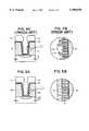
- FIGS. 1-3are section views showing a conventional aperture (contact hole) buried wiring structure, wherein various problems which may arise in filling a contact hole are exemplified.
- an impurity diffusion region 4which will become a source/drain region, is formed on a semiconductor substrate 2.
- an insulating layer 8having a contact hole 6 for partially exposing the surface of impurity diffusion region 4 is formed on the resultant structure.
- a gate electrode in MOS structureis not shown.
- a titanium layer as an ohmic contact layer (not shown) and a TiN layer 10 as a diffusion barrier layerare sequentially formed on the inner sidewall surface of contact hole 6, on impurity diffusion region 4 exposed by contact hole 6 and on insulating layer 8.
- an aluminum layer 12 for filling contact hole 6is formed on TiN layer 10.
- the above-described contact hole buried wiring structurecan be manufactured as follows.
- a field oxide film(not shown) is formed on semiconductor substrate 2 by a common local oxidation of silicon (LOCOS) method, and an impurity is deposited on semiconductor substrate 2 between the field oxide films, to thereby form impurity diffusion region 4 for forming a source/drain region.
- an insulating materialfor example, silicon oxide (SiO 2 )
- CVDcommon chemical vapor deposition
- a photoresist pattern(not shown) for forming contact hole 6 is formed on insulating layer 8 which is then etched until impurity diffusion region 4 is exposed, using the photoresist pattern as an etching mask, to thereby form aperture 6.
- titaniumis deposited to a thickness of 300 ⁇ to 900 ⁇ by a sputtering method on the inner sidewall surface of aperture 6, on impurity diffusion region 4 exposed by aperture 6 and on insulating layer 8, to thereby form the ohmic contact layer.
- the diffusion barrier layer(layer 10) is formed on the Ti layer to a thickness of 600 ⁇ to 2000 ⁇ by a sputtering method.
- Aluminumis deposited on the resultant structure by a sputtering method, to thereby form aluminum layer 12 for burying aperture 6.
- a Ti layeri.e., ohmic contact layer
- a TiN layer 10i.e., diffusion barrier layer
- an Al layer 12are formed by mainly a sputtering method.
- deposition by a conventional sputtering methodcauses a void 14 as shown in FIGS. 1 and 2, as the aspect ratio of the contact hole increases, to thereby degrade the reliability of a manufactured device.
- the step coverage of an aluminum layeris poor, as shown in FIG. 3, so that wiring shorts tend to occur. Thus, a reliability of the device is degraded.
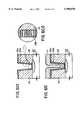
- FIG. 4illustrates an initial nucleation of an aluminum film when aluminum is deposited on the diffusion barrier film shown in FIGS. 1-3, and includes an enlarged view of the sidewall portion showing the initial nucleation.
- a reference numeral 10denotes a TiN layer
- 10adenotes a TiN grain
- 12denotes an aluminum layer
- 12adenotes an aluminum grain.
- a TiN layer obtained by a sputtering method or CVD methodis not amorphous. Therefore, the inner sidewalls of the contact hole where relatively few sputtered atoms are formed has a rough surface. Accordingly, an initial deposition characteristic of an aluminum atom formed on the rough diffusion barrier film is poor. In other words, a nucleation of aluminum around the relatively large TiN grains does not occur uniformly, and the aluminum is deposited unevenly and discontinuously as shown in the enlarged view. Therefore, even though heat treatment is performed by depositing aluminum in a contact hole during a subsequent process, a void is generated, and generation of such a void becomes easier in a contact hole having a high aspect ratio. Thus, reliability of a semiconductor device is degraded.
- a wiring structure of a semiconductor devicecomprising: a semiconductor substrate; an insulating layer formed on the semiconductor substrate and including an aperture formed therein; a diffusion barrier film which has a smooth surface formed through a plasma irradiation on both sidewalls of the aperture; and a metal layer formed on the diffusion barrier film.
- the diffusion barrier filmconsists of a refractory metal or a refractory metal compound.
- the refractory metalmay be Ti and the refractory metal compound may be TiN.
- the apertureis a contact hole for exposing an impurity diffusion region of the semiconductor substrate or a via hole for exposing a lower conductive layer.
- the metal layermay be formed of aluminum or aluminum alloy.
- a wiring structure of a semiconductor devicecomprising: a semiconductor substrate; an insulating layer formed on the semiconductor substrate and including an aperture formed therein; a diffusion barrier film which has a smooth surface formed through a plasma irradiation on both sidewalls of the aperture; and a metal layer buried in the aperture where the diffusion barrier film is formed.
- a method for forming a wiring structure of a semiconductor devicecomprising the steps of: forming an insulating layer on a semiconductor substrate; forming an aperture on the insulating layer; forming a diffusion barrier film on the insulating layer, on the substrate exposed by the aperture and on the inner sidewalls of the aperture; plasma irradiating the surface of the diffusion barrier film formed on the inner sidewalls of the aperture; and forming a metal layer on the plasma-irradiated diffusion barrier film.
- plasmais employed for smoothing the surface of the diffusion barrier film.
- the plasmais formed by an electron cyclotron resonance (ECR) plasma using an inert gas, an RF plasma device or a magnetron-enhanced plasma device.
- ECRelectron cyclotron resonance
- a plasma processing effectcan be enhanced by adding hydrogen to the inert gas.
- the metal layercan be formed by a chemical vapor deposition (CVD) method, and a heat treatment can be further performed after the step of forming the diffusion barrier film.
- a step of performing a heat treatment to bury the aperturecan be further comprised after the step of forming the metal layer.
- the method of the present inventionmay further comprise the step of forming a second metal layer after the step of burying the aperture.
- the metal layercan be formed through two deposition processes, firstly deposited at a first temperature, and secondly at a second temperature. The first temperature should to be lower than the second temperature.
- an insulating layer on a semiconductor substratecomprising the steps of: forming an aperture on the insulating layer; forming a first diffusion barrier film on the insulating layer, on the substrate exposed by the aperture, and on the inner sidewalls of the aperture; plasma irradiating a surface of the first diffusion barrier film formed on the sidewalls of the aperture; forming a second diffusion barrier film on the plasma-irradiated first diffusion barrier film; forming a metal layer all over the substrate where the second diffusion barrier film is formed; and burying the aperture by performing a heat treatment on the metal layer.
- the metal layercan be subsequently formed without breaking a vacuum after the second diffusion barrier film is formed.
- a step of forming a second metal layercan be further comprised after the step of forming the metal layer.
- a heat treatmentcan be performed after the step of forming the second diffusion barrier film. And, a heat treatment can be performed after the step of plasma irradiating a surface of the first diffusion barrier film.
- a method for forming a wire of a semiconductor devicecomprising the steps of: forming an insulating layer on a semiconductor substrate; forming an aperture on the insulating layer; forming a first diffusion barrier film on the insulating layer, on the substrate exposed by the aperture, and on the inner sidewalls of the aperture; plasma irradiating a surface of the first diffusion barrier film formed on the sidewalls of the aperture; forming a second diffusion barrier film on the plasma-irradiated first diffusion barrier film; and performing a high temperature sputtering all over the substrate where the second diffusion barrier film is formed so as to bury the aperture.
- the metal layeri.e., an aluminum film
- the smooth diffusion barrier filmsuch that an aluminum film is uniformly and continuously deposited to have an excellent step coverage. Accordingly, a contact hole having a high step coverage can be effectively buried, to thereby enhance a reliability of a device.
- FIGS. 1, 2 and 3are section views showing the various problems of a conventional buried wiring structure
- FIG. 4illustrates an initial nucleation of an aluminum film when aluminum is deposited on the diffusion barrier film shown in FIGS. 1-3;
- FIG. 5illustrates a wire layer structure of the semiconductor device of the present invention and the initial nucleation of a metal layer on the sidewall of an aperture
- FIGS. 6A-6Dshow embodiment 1 of a method for forming a wire layer of a semiconductor device of the present invention, wherein FIGS. 6B and 6C include an enlarged view showing the surface of the diffusion barrier film formed on the sidewall of the aperture;
- FIGS. 7A-7Care section views of embodiment 2 of a method for forming a wire layer of a semiconductor device of the present invention.
- FIGS. 8A-8Care section views of embodiment 3 of a method for forming a wire layer of a semiconductor device of the present invention.
- FIGS. 9A-9Care section views of embodiment 5 of a method for forming a wire layer of a semiconductor device of the present invention, wherein FIG. 9A includes an enlarged view showing the surface of the diffusion barrier film formed on the sidewall of the aperture;
- FIGS. 10A-10Care section views of embodiment 6 of a method for forming a wire layer of a semiconductor device of the present invention.
- FIGS. 11 and 12are SEM photos of a TiN surface which is plasma-irradiated according to the present invention and a conventional TiN surface which is not plasma-irradiated, respectively.
- an impurity diffusion region 33which will become a source/drain region is formed on a semiconductor substrate 31.
- the impuritycan be either N + or P + type and a field oxide film (not shown) can be formed to the right and left of the impurity diffusion region.
- impurity diffusion region 33 formed in semiconductor substrate 31is merely an embodiment of a silicon layer suitable for accomplishing the object of the present invention, which is to provide a contact hole buried structure for burying an upper conductive layer in a silicon layer in a lower portion of an aperture, e.g., contact hole or via hole.
- impurity diffusion region 33 formed in the semiconductor substratecan be replaced by a lower conductive layer (not shown), for example, a polysilicon layer formed on an arbitrary lower structure atop the semiconductor substrate.
- a contact hole buried structure(described later) can be applied to the via hole buried structure formed on the lower conductive layer.
- Insulating layer 35having an aperture (contact hole) for exposing the impurity diffusion region is formed on the resultant structure.
- Insulating layer 35consists of insulating materials, for example, silicon oxide.
- the aperturemay be a contact hole for exposing impurity diffusion region 33 or a via hole for exposing a lower conductive layer, for example, polysilicon.
- the diffusion barrier film 37can be a TiN layer formed on a Ti layer (not shown). The Ti layer is formed on the inside surface of the aperture, on impurity diffusion region 33 exposed by the aperture and on insulating layer 35.
- the diffusion barrier film 37can also be a Ti layer.
- an initial nucleation of the metal layeris shown in a detailed view of the diffusion barrier film and metal layer formed on the sidewall of the aperture.
- a smooth diffusion barrier film 37 without having grain boundariesis formed on the sidewall of the aperture.
- An initial deposition characteristic of the aluminum atoms on the sidewall of diffusion barrier film 37is excellent.
- a nucleation of an aluminum filmoccurs uniformly due to the uniform TiN grain or smooth surface of TiN film. Accordingly, the aluminum film is deposited uniformly and continuously, different from a conventional technique.
- FIGS. 6A-6Dare section views showing embodiment 1 of a method for forming a wire layer of a semiconductor device of the present invention, with FIGS. 6B and 6C including enlarged views showing a surface of the diffusion barrier film formed on the inner sidewalls of the aperture.
- FIG. 6Ashows the step of forming insulating layer 35 having an aperture on semiconductor substrate 31.
- a field oxide film(not shown) is formed on semiconductor substrate 31 by a general LOCOS method, and an N + or P + type impurity is implanted on semiconductor substrate 31 between field oxide films, to thereby form impurity diffusion region 33 for forming a source/drain region.
- the process of forming the field oxide filmis arbitrary, and the impurity diffusion region can be replaced by an arbitrary silicon layer, for example, polysilicon, according to the object of the present invention.
- An insulating materialfor example, silicon oxide (SiO 2 ), is deposited on the resultant structure by a general CVD method, to thereby form an insulating material layer.
- the insulating material layeris formed to a thickness of 0.8 ⁇ m to 1.6 ⁇ m by employing a borophosphorous silicate glass (BPSG).
- BPSGborophosphorous silicate glass
- a photoresist pattern(not shown) for forming an aperture is formed on the insulating material layer.
- the photoresist patternas an etching mask, the insulating material layer is etched until impurity diffusion region 33 is exposed, to thereby form insulating layer 35 having an aperture.
- FIG. 6Bshows the step of forming diffusion barrier film 37 all over the substrate where the aperture is formed.
- Diffusion barrier film 37is formed all over insulating layer 35, inside an aperture 36 and on the exposed surface of semiconductor substrate 31.
- Tiis deposited to a thickness of 200 ⁇ to 300 ⁇ by a sputtering method in an argon atmosphere at 2 mTorr to form a Ti layer
- titanium nitrideis deposited to a thickness of 300 ⁇ to 500 ⁇ by a sputtering method under the condition where an amount of argon gas is 30-50 sccm and an amount of nitrogen is 50-85 sccm so as to form diffusion barrier film 37.
- the deposition speedis approximately 500 ⁇ per minute when the Ti layer is deposited.
- the substrate temperatureis 200° when Ti or TiN is deposited.
- the Ti layer or TiNwhen the Ti layer or TiN is deposited, a collimation technique can be employed.
- the size of the collimatoris 5/8" and the aspect ratio is 1.5:1.
- the TiN layer formed on the sidewalls of the aperturehas a rough surface in the sidewalls of the contact hole where a relatively small number of the sputtered atoms are formed, as shown in the enlarged view of FIG. 6B.
- FIG. 6Cshows the step of plasma irradiating the surface of TiN layer 37.
- TiN layer 37is eroded by employing an argon plasma, and the plasma irradiating is performed using an ECR(electron cyclotron resonance) plasma, RF plasma or a magnetron-enhanced plasma device.
- ECRelectron cyclotron resonance
- the surface of the TiN layeris eroded through a collision between the TiN layer formed on the sidewalls and argon ions (Ar + ) or through absorption of the momentum of argon ions in TiN layer.
- argon ionsAr +
- absorption of the momentum of argon ions in TiN layerAs a result, a TiN layer 39b having a smooth surface without having grain boundaries and a TiN layer 39a having a rough surface are formed.
- TiN layer 37is plasma-irradiated at the state where an RF bias of approximately 50V is applied by employing ECR plasma.
- the ECR plasma deviceperforms the process under a condition where microwave power is 1 kW (magnetron frequency: 2.45 GHz), an argon pressure is 5 mTorr and a substrate temperature is room ambient.
- the TiN layeris etched approximately by 30 ⁇ when a standard oxide film (SiO 2 ) is etched by 100 ⁇ .
- a small biasmay be applied to a substrate and a surface treatment effect can be increased by adding hydrogen.
- the sputtering deviceperforms a plasma irradiating under a condition where frequency is 13.56 MHz, bias voltage is 960V, an argon atmosphere is 7 mTorr and substrate temperature is 200° C.
- the sputter etching by plasma irradiatingis performed by having 100 ⁇ of oxide film (SiO 2 ) as a standard. The effect is the same when an etching is performed for an standard oxide film exceeding 100 ⁇ .
- the rough surface of the TiN grains on the sidewalls of the apertureis eroded, thereby forming a TiN layer with a smooth surface, as shown in the enlarged view of FIG. 6C.
- FIG. 6Dshows the step of forming metal layer 41 for burying an aperture.
- metal layer 41is deposited on the inner sidewalls of the aperture and impurity diffusion region 33 exposed by the aperture by a sputtering method, to thereby form metal layer 41 for burying the aperture.
- deposition of metal layer 41is performed under a condition where a deposition temperature is 200° C., an argon pressure is 4 mTorr and a deposition speed is 50 to 150 ⁇ per second. It is more desirable to control the deposition speed to 125 ⁇ per second.
- a deposition characteristic and step coverageare enhanced.
- an aluminumis firstly deposited under a condition where the temperature is below 100° C. and deposition speed is 50 ⁇ to 150 ⁇ per second. Then, the aluminum is deposited at a temperature higher than 200° C. and at a higher deposition speed of 100 ⁇ to 150 ⁇ per second.
- an excellent step coverage at a low temperature and an atom mobility improvement at a high temperaturecan be simultaneously obtained.
- FIGS. 7A-7Care section views of embodiment 2 of a method for forming a wire layer of a semiconductor device of the present invention.
- Embodiment 2is the same as embodiment 1 except for a step of forming a metal layer at a low temperature and a step of performing a vacuum heat treatment.
- like elementsare denoted by the same reference numerals as those of embodiment 1.
- the first steps performed in embodiment 2are the same as those corresponding to FIGS. 6A-6C in embodiment 1.
- FIG. 7Ashows the step of forming a first metal layer 43a.
- a first metal layer 43aconsisting of aluminum or an aluminum alloy (for example, Al--Si--Cu) is formed on the inner sidewalls of an aperture, on a substrate exposed by the aperture and on a diffusion barrier film.
- First metal layer 43ais formed by employing a DC magnetron device under a condition where the temperature is lower than 200° C. (desirably, low temperature of 25° C.), the degree of vacuum is below 5.0E-7 Torr (more desirably, below 5.0E-8 Torr) and deposition speed is 100 ⁇ per second.
- low pressure sputtering or collimationcan be employed under a condition where working pressure is below 2 mTorr in order to reduce an overhang phenomenon at the top of the aperture.
- FIG. 7Bshows the step of performing a heat treatment on first metal layer 43a.
- first metal layer 43a formed on the apertureis vacuum-heat-treated by means of raising the temperature of the DC magnetron device or transferring the substrate to a chamber having a high temperature.
- the vacuum heat treatmentis performed in such a way that first metal layer 43a is heat-treated for two minutes without a vacuum break under a condition where the temperature is 50% to 90% of a melting point of the aluminum alloy, for example, above 450° C., and in an argon or reduction atmosphere below 10 mTorr, to thereby move the atoms of the aluminum alloy which is sputtered at a low temperature.
- the apertureis buried as shown in FIG. 7B so as to form the buried first metal layer 43b.
- the temperature of the heat treatmentcan be lowered as the degree of vacuum is enhanced when deposition or vacuum heat treatment is performed.
- FIG. 7Cshows the step of forming second metal layer 47 on the buried first metal layer 43b.
- a second metal layer 47is formed by using the same material as that of first metal layer 43a on the buried first metal layer 43b.
- the step of forming second metal layer 47may be unnecessary in the case where the overhang phenomenon occurs less because first metal layer 43a is formed to a desired thickness and heat-treated so as to bury the aperture.
- FIGS. 8A-8Care section views of embodiment 3 of a method for forming a wire layer of a semiconductor device of the present invention.
- Embodiment 3is the same as embodiment 2 except that first metal layers 43c and 43d are formed by firstly depositing a metal material at a temperature below 200° C. and secondly at a temperature above 400° C.
- first metal layers 43c and 43dare formed by firstly depositing a metal material at a temperature below 200° C. and secondly at a temperature above 400° C.
- like elementsare denoted by the same reference numerals as those of embodiment 2.
- the first steps performed in embodiment 3are the same as those corresponding to FIGS. 6A-6C in embodiment 1.
- FIG. 8Ashows the step of forming first metal layers 43c and 43d.
- first metal layers 43c and 43dconsisting of Al--Si--Cu are formed on the sidewalls of an aperture, on the substrate exposed by the aperture and on a diffusion barrier film.
- first metal layers 43c and 43dare formed through the following process.
- Aluminum or an aluminum alloy(for example, Al--Si--Cu) is firstly deposited to a thickness of less than half of the desired thickness at a temperature of 200° C. or below, and an aluminum alloy of Al--Si--Cu is secondly deposited at a desirable temperature of 450° C.
- the deposition speedhas to be lower than 100 ⁇ per second at a low temperature, i.e., 200° C. or below, and 150 ⁇ per second at a high temperature, i.e., 400° C. or above.
- FIG. 8Bshows the step of performing a heat treatment on first metal layers 43c and 43d.
- first metal layers 43c and 43d formed on the apertureis vacuum-heat-treated by means of raising the temperature of a DC magnetron device or transferring the substrate to a chamber having a high temperature.
- Surface atoms of aluminummove due to such vacuum heat treatment, and thus the aperture is buried as shown in FIG. 8B so as to form the buried first metal layer 43e.
- the temperature of the heat treatmentcan be lowered as the degree of vacuum is enhanced when deposition or vacuum heat treatment is performed.
- FIG. 8Cshows the step of forming a second metal layer 49 on the buried first metal layer 43b.
- second metal layer 49is formed by using the same material as that of first metal layers 43c and 43d on the buried first metal layer 43e.
- the step of forming second metal layer 49may be unnecessary because first metal layer 43b can be formed to a desired thickness and heat-treated so as to bury the aperture.
- Embodiment 4is the same as embodiment 3 except that a second vacuum heat treatment is performed after the second metal layer is formed in embodiment 3.
- the process steps of embodiment 3are performed in sequence, and a second vacuum heat treatment is performed subsequently.
- the second vacuum heat treatmentis performed at a temperature of the first vacuum heat treatment, for example, 450° C. Or, the second vacuum heat treatment is performed at a low temperature of the first vacuum heat treatment.
- FIGS. 9A-9Care section views showing embodiment 5 of a method for forming a wire layer of a semiconductor device of the present invention, wherein FIG. 9A includes an enlarged view showing a surface of a diffusion barrier film formed on the sidewall of the aperture.
- Embodiment 5is the same as embodiments 3 and 4 except that a second diffusion barrier film is formed prior to forming a first metal layer.
- like elementsare denoted by the same reference numerals as those of embodiment 4.
- the first steps performed in embodiment 5are the same as those corresponding to FIGS. 6A-6C in embodiment 1.
- FIG. 9Ashows the step of forming a second diffusion barrier film 42 and a first metal layer 43f.
- the first diffusion barrier filmis heat-treated in a nitrogen atmosphere of 450° C., to thereby enhance the thermal endurance of the diffusion barrier film.
- Such an enhancement in thermal enduranceresults from an oxygen stuffing effect and silicidation in the Ti layer formed under the TiN layer.
- Al 3 Tiis formed.
- junction spikingoccurs at a temperature of 450° C. due to silicon and Al 3 Ti having a high solubility.
- a reaction between Ti and Siproduces TiSi 2 /TiN structure, to thereby enhance thermal endurance of the diffusion barrier film.
- a first diffusion barrier filmi.e., TiN, keeps a smooth surface on the sidewalls of the aperture after heat-treatment is performed.
- second diffusion barrier film 42is formed by depositing Ti or TiN to a thickness of 100 ⁇ to 200 ⁇ on the sidewalls of the aperture, on the substrate exposed by the aperture and on the first diffusion barrier film, in order to enhance a wettability of aluminum film.
- TiN graini.e., second diffusion barrier film 42, is formed into extremely small and regular size on the smooth surface of the sidewall of the aperture.
- First metal layer 43fconsisting of aluminum or an aluminum alloy, i.e., Al--Si--Cu, is formed. Since the TiN grain is formed of extremely small and regular size on the smooth surface of the sidewalls of the aperture, an initial nucleation of the first metal layer occurs uniformly, and an excellent step coverage can be formed. First metal layer 43f can be formed through two steps as in embodiments 3 and 4.
- FIG. 9Bshows the step of performing heat treatment on first metal layer 43f.
- first metal layer 43f formed on the apertureis vacuum-heat-treated.
- Surface atoms of an aluminum filmmove to the aperture and are buried due to the vacuum heat treatment as shown in FIG. 9B, to thereby form a buried first metal layer 43g.
- the buried first metal layer 43gexhibits uniform nucleation in an early stage of an aluminum deposition and has an excellent step coverage, a burying characteristic is enhanced when heat-treatment is performed. As a result, the reliability in a semiconductor device can be enhanced.
- the buried first metal layercan be formed by a high temperature sputtering at a temperature exceeding 400° C.
- FIG. 9Cshows the step of forming a second metal layer 51 on the buried first metal layer 43g.
- second metal layer 51is formed on the buried first metal layer 43g by using the same material as that of first metal layer 43g.
- the step of forming second metal layer 51may be unnecessary because first metal layer 43g may be formed to a desired thickness and heat-treated so as to bury the aperture.
- FIGS. 10A-10Care section views showing embodiment 6 of a method for forming a wire layer of a semiconductor device of the present invention.
- Embodiment 6is the same as embodiments 2 to 5 except that, after a first metal layer is formed by CVD method, the first metal layer is vacuum heat-treated, or an aluminum alloy is sputtered on the first metal layer and vacuum heat-treated, so as to bury an aperture.
- like elementsare denoted by the same reference numerals as those of embodiment 2.
- the first steps performed in embodiment 6are the same as those corresponding to FIGS. 6A-6C in embodiment 1.
- FIG. 10Ashows the step of forming a first metal layer 43h.
- First metal layer 43h consisting of aluminumis formed by a CVD method on the sidewalls of an aperture, on a substrate exposed by the aperture and on a diffusion barrier film.
- the deposition of aluminum or an aluminum alloycan be performed by a common CVD method.
- the depositioncan be performed by using an organic metal compound, e.g., triisobutyl aluminum (TIBA) or dimethyl aluminum hydride ((CH 3 ) 2 AlH: DMAH), as a source.
- TIBAtriisobutyl aluminum
- DMAHdimethyl aluminum hydride
- a cold-wall-type apparatusis employed to maintain a vapor temperature below 90° C., and desirably at 84-86° C., when the TIBA is introduced.
- inert gasfor example, argon
- the desirable flow speed of the argon gasis approximately 71 per minute.
- the deposition temperature at a thermal decomposition of the TIBAis approximately 250° C., which is not desirable because the deposition speed is high. Since the deposition speed decreases as the temperature is lowered, the deposition can be performed at a lower temperature in order to reduce the deposition speed. Under such conditions, the deposition speed is approximately 1,000 ⁇ per minute, and the aluminum is deposited approximately for one minute by employing TIBA for a contact hole size of 0.2 ⁇ m.
- first metal layer 43his deposited by using an aluminum hydrogen, for example, DMAH, etc.
- an aluminum hydrogenfor example, DMAH, etc.
- the aluminum hydrogenis preserved at a low temperature and the deposition is performed at a temperature exceeding 50° C. in order to prevent a thermal decomposition of the aluminum hydrogen.
- the temperature of the sourcecan be controlled by employing an inert gas, i.e., argon.
- the temperature of the substrateis lowered or an amount of the source is decreased so as to reduce a deposition speed.
- deposition temperaturecan be lowered by using a suitable source.
- the depositionis performed in a reactive chamber where the pressure is 0.01-1.0 Torr and temperature is 50-150° C. Since first metal layer 43h is formed by the CVD method on the smooth surface of the TiN formed on the sidewalls of the aperture, an excellent step coverage is achieved, as shown in FIG. 10A.
- FIG. 10Bshows the step of burying an aperture by performing a heat treatment on first metal layer 43h.
- first metal layer 43h formed on the apertureis vacuum-heat-treated without breaking the vacuum, or an aluminum alloy, for example, Al--Si--Cu, is sputtered on the first metal layer 43h and vacuum heat-treated.
- Surface atoms of the aluminum filmmove due to the vacuum heat treatment so as to bury the aperture as shown in FIG. 10B, thereby forming the buried first metal layer 43i.
- the temperature of the heat treatmentcan be lowered as the degree of vacuum increases when a deposition or vacuum heat treatment is performed.
- the aperturecan be buried without having a seam or void.
- the aperturecan be buried without performing the vacuum heat treatment. If the seam or void is generated, it can be removed by subsequent vacuum heat treatment. Accordingly, the vacuum heat treatment is optional.
- FIG. 10Cshows the step of forming second metal layer 53 on the buried first metal layer 43i.
- second metal layer 53is formed by using the same material as that of first metal layer 43i on the buried first metal layer 43i by a sputtering method.
- the same material as that of first metal layer 43iis sputtered on the buried first metal layer 43i so as to form second metal layer 53 which will be vacuum-heat-treated.
- the step of forming second metal layer 53may be unnecessary because first metal layer 43h can be formed to a desired thickness and heat-treated so as to bury the aperture.
- FIGS. 11 and 12are SEM photos of a TiN surface which is plasma-irradiated according to the present invention and a conventional TiN surface which is not plasma-irradiated, respectively.
- the surface of the TiNis smooth and has no grain boundaries.
- the surface of the TiN of a conventional techniqueis rough.
- an aluminum film of the metal layeris formed uniformly and continuously.
- an aluminum film of the metal layer formed on the sidewall of the smooth diffusion barrier filmhas a good step coverage. Therefore, a contact hole having a high aspect ratio can be effectively buried without producing a void therein, to thereby enhance the reliability of a manufactured device.
Landscapes
- Engineering & Computer Science (AREA)
- Physics & Mathematics (AREA)
- Condensed Matter Physics & Semiconductors (AREA)
- General Physics & Mathematics (AREA)
- Manufacturing & Machinery (AREA)
- Computer Hardware Design (AREA)
- Microelectronics & Electronic Packaging (AREA)
- Power Engineering (AREA)
- Plasma & Fusion (AREA)
- Internal Circuitry In Semiconductor Integrated Circuit Devices (AREA)
- Electrodes Of Semiconductors (AREA)
Abstract
Description
This is a Continuation of National Appln. Ser. No. 08/476,111 filed Jun. 7, 1995, now abandoned.
The present invention relates to a method for manufacturing a semiconductor device, and more particularly, to a wiring structure of a semiconductor device for burying an aperture such as a contact hole or a via hole and a method for manufacturing the same.
Generally speaking, the most crucial part in the manufacturing process of a semiconductor device is the wiring, because the operating speed, yield and reliability of the device are all determined by the wiring method. The step coverage of a metal layer is not a significant problem in a conventional semiconductor device having low integration. However, recently, higher integration levels have resulted in extremely small contact holes (i.e., diameters of one half micron or less) and very thin impurity injection regions in the semiconductor substrate. Using conventional aluminum wiring methods, it is difficult to fill a contact hole smaller than 1 μm, and a void is often formed in the contact hole, and which lowers the reliability of the metal wiring layer.
In an early stage of manufacturing a semiconductor device, a metal wiring layer is formed on a silicon substrate by using pure aluminum. However, as temperature increases in a subsequent sintering stage, the formed aluminum layer absorbs silicon atoms from the substrate, which generates junction (Al) spiking. Therefore, Al-1% Si (aluminum supersaturated with silicon) has been widely used as the material of the metal wiring layer.
However, when the wiring of a semiconductor device is formed using Al-1% Si, silicon is extracted from the aluminum film during heat treatment at a temperature exceeding 450° C., thus forming a silicon residue. In addition, a Si-nodule is formed in a contact hole through the solid-phase epitaxial growth of silicon atoms, to thereby increase the wiring resistance and contact resistance.
To prevent the above Al spiking, the generation of silicon residue and the Si-nodule due to an interaction between a metal wire layer and a silicon substrate, a diffusion barrier film is formed between the wiring layer and silicon substrate or between the wiring layer and an insulating layer. For example, a method for forming a titanium nitride (TiN) film as a diffusion barrier film on an inner wall of a contact hole is disclosed in U.S. Pat. No. 4,897,709 by Yokoyama et al. In addition, a technique where a double film consisting of a refractory metal (Ti) film and a TiN film is formed and heat-treated as a diffusion barrier layer, and a titanium (Ti) layer interacts with a semiconductor substrate to thus form a refractory metal silicide layer consisting of thermally stable compounds in the bottom of a contact hole connected to the semiconductor substrate, to thereby enhance a barrier effect, is disclosed in Japanese Laid-open Publication No. 61-183942. In general, such a diffusion barrier film is annealed in a nitrogen atmosphere. If the diffusion barrier film is not annealed, junction spiking occurs when aluminum or an aluminum alloy is sputtered at a temperature exceeding 450° C. or when sintering is performed, which is not desirable. In addition, a TiN or TiW film is employed as the diffusion barrier film. A microstructural defect that cannot completely prevent the diffusion of aluminum or silicon at a grain boundary exists in the TiN or TiW film.
In addition, a method for blocking a diffusion path at a grain boundary by employing an oxygen stuffing method has been proposed (see: pp375-382 of "Effects of Oxygen on Reactively Sputtered TiN Films" by J. B. Stimmel and B. N. Mehrotra, in Tungsten and Other Refractory Metals for VLSI Application III, 1988). In general, when TiN is deposited and exposed to the ambient atmosphere, the exposed TiN is mixed with a small amount of oxygen in the atmosphere, to thereby increase a diffusion barrier effect. This is called a stuffing effect. In more detail, Stimmel and Mehrotra teach that oxygen exists in oxide form at a surface of barrier metal and at a grain boundary as well, which explains a stuffing effect.
However, a contact resistance may increase if a barrier layer formed by depositing Ti or TiN is exposed to the atmosphere, or if the TiN is deposited by mixing with oxygen, or if TiN is annealed at a nitrogen atmosphere mixed with oxygen. Accordingly, the barrier characteristic of a TiN film changes depending on the duration of atmospheric exposure, the amount of oxygen inflowed during deposition, the amount of oxygen in annealing, and the temperature. Annealing of the barrier layer is performed at a temperature of 450° C. to 550° C. under a N2 atmosphere for 30-60 minutes, which is known as an optimum condition.
However, the oxygen stuffing effect introduced when a diffusion barrier film is annealed causes oxidation of the surface of the diffusion barrier film, and thus causes problems such as contact characteristics when a contact hole is buried by using aluminum in the subsequent process. Thus, the oxygen stuffing effect degrades reliability of a semiconductor device. To suppress this degradation, a method for inserting a wetting layer for improving wettability of the metal layer and a method for burying a contact hole after forming a silylation layer and hydrogen-treating are proposed.
In another method, Si or O2 is ion-injected after a TiN layer, i.e., barrier layer, is heat-treated in order to enhance wettability between the barrier metal and aluminum wiring and to enhance a wiring quality and yield (Japanese Laid-open Publication No. 88-176035 by Higatta Masafumi).
In yet another disclosure, in the case where Ti is deposited in advance to an aluminum sputtering and a high temperature aluminum is subsequently deposited so as to fill a via hole whose size is 0.5 μm and aspect ratio is 1.6, a filling-up effect decreases if Ti is thin (see: VMIC 170-176, 1991). However, as the size of a contact hole becomes smaller, i.e., below 0.5 μm, the contact hole is not completely filled or a void is generated in the contact hole, to thereby degrade reliability.
FIGS. 1-3 are section views showing a conventional aperture (contact hole) buried wiring structure, wherein various problems which may arise in filling a contact hole are exemplified. First, animpurity diffusion region 4, which will become a source/drain region, is formed on asemiconductor substrate 2. Then, aninsulating layer 8 having a contact hole 6 for partially exposing the surface ofimpurity diffusion region 4 is formed on the resultant structure. (Here, for the convenience of explanation, a gate electrode in MOS structure is not shown.) A titanium layer as an ohmic contact layer (not shown) and aTiN layer 10 as a diffusion barrier layer are sequentially formed on the inner sidewall surface of contact hole 6, onimpurity diffusion region 4 exposed by contact hole 6 and oninsulating layer 8. In addition, analuminum layer 12 for filling contact hole 6 is formed onTiN layer 10.
Meanwhile, the above-described contact hole buried wiring structure can be manufactured as follows.
First, a field oxide film (not shown) is formed onsemiconductor substrate 2 by a common local oxidation of silicon (LOCOS) method, and an impurity is deposited onsemiconductor substrate 2 between the field oxide films, to thereby formimpurity diffusion region 4 for forming a source/drain region. Then, an insulating material, for example, silicon oxide (SiO2), is deposited on the resultant structure by a common chemical vapor deposition (CVD) method, thereby forming insulatinglayer 8. Then, a photoresist pattern (not shown) for forming contact hole 6 is formed on insulatinglayer 8 which is then etched untilimpurity diffusion region 4 is exposed, using the photoresist pattern as an etching mask, to thereby form aperture 6. Then, titanium is deposited to a thickness of 300 Å to 900 Å by a sputtering method on the inner sidewall surface of aperture 6, onimpurity diffusion region 4 exposed by aperture 6 and oninsulating layer 8, to thereby form the ohmic contact layer. Sequentially, the diffusion barrier layer (layer 10) is formed on the Ti layer to a thickness of 600 Å to 2000 Å by a sputtering method. Aluminum is deposited on the resultant structure by a sputtering method, to thereby formaluminum layer 12 for burying aperture 6.
In the above-described conventional contact hole buried wiring structure and a method for manufacturing the same, a Ti layer (i.e., ohmic contact layer), a TiN layer 10 (i.e., diffusion barrier layer), and anAl layer 12 are formed by mainly a sputtering method. However, deposition by a conventional sputtering method causes avoid 14 as shown in FIGS. 1 and 2, as the aspect ratio of the contact hole increases, to thereby degrade the reliability of a manufactured device. Also, according to the conventional technique, the step coverage of an aluminum layer is poor, as shown in FIG. 3, so that wiring shorts tend to occur. Thus, a reliability of the device is degraded.
FIG. 4 illustrates an initial nucleation of an aluminum film when aluminum is deposited on the diffusion barrier film shown in FIGS. 1-3, and includes an enlarged view of the sidewall portion showing the initial nucleation. Here, areference numeral 10 denotes a TiN layer, 10a denotes a TiN grain, 12 denotes an aluminum layer, and 12a denotes an aluminum grain. A characteristic of the TiN layer formed in the inner sidewalls of an aperture and a surface morphology of an aluminum layer will be explained with reference to FIG. 4.
Since the surface of the TiN layer formed on the inner sidewall surface of an aperture is structurally perpendicular to the target when deposition is performed, a relatively small amount of sputtered atoms are deposited. Such tendency occurs obviously when a collimation technique is employed. In addition, since TiN is apt to grow in the <111> direction,columnar grains 10a are formed.
Meanwhile, in general, a TiN layer obtained by a sputtering method or CVD method is not amorphous. Therefore, the inner sidewalls of the contact hole where relatively few sputtered atoms are formed has a rough surface. Accordingly, an initial deposition characteristic of an aluminum atom formed on the rough diffusion barrier film is poor. In other words, a nucleation of aluminum around the relatively large TiN grains does not occur uniformly, and the aluminum is deposited unevenly and discontinuously as shown in the enlarged view. Therefore, even though heat treatment is performed by depositing aluminum in a contact hole during a subsequent process, a void is generated, and generation of such a void becomes easier in a contact hole having a high aspect ratio. Thus, reliability of a semiconductor device is degraded.
Accordingly, it is an object of the present invention to provide a wiring structure of a semiconductor device for forming a smooth surface of a diffusion barrier film so as to effectively bury a contact hole having a high step.
It is another object of the present invention to provide a method for suitably forming a wiring structure of a semiconductor device provided with a diffusion barrier film having a smooth surface.
To accomplish the above object of the present invention, there is provided a wiring structure of a semiconductor device comprising: a semiconductor substrate; an insulating layer formed on the semiconductor substrate and including an aperture formed therein; a diffusion barrier film which has a smooth surface formed through a plasma irradiation on both sidewalls of the aperture; and a metal layer formed on the diffusion barrier film.
The diffusion barrier film consists of a refractory metal or a refractory metal compound. Specifically, the refractory metal may be Ti and the refractory metal compound may be TiN. In addition, the aperture is a contact hole for exposing an impurity diffusion region of the semiconductor substrate or a via hole for exposing a lower conductive layer. The metal layer may be formed of aluminum or aluminum alloy.
There is also provided a wiring structure of a semiconductor device comprising: a semiconductor substrate; an insulating layer formed on the semiconductor substrate and including an aperture formed therein; a diffusion barrier film which has a smooth surface formed through a plasma irradiation on both sidewalls of the aperture; and a metal layer buried in the aperture where the diffusion barrier film is formed.
There is provided a method for forming a wiring structure of a semiconductor device comprising the steps of: forming an insulating layer on a semiconductor substrate; forming an aperture on the insulating layer; forming a diffusion barrier film on the insulating layer, on the substrate exposed by the aperture and on the inner sidewalls of the aperture; plasma irradiating the surface of the diffusion barrier film formed on the inner sidewalls of the aperture; and forming a metal layer on the plasma-irradiated diffusion barrier film.
In the present invention, plasma is employed for smoothing the surface of the diffusion barrier film. The plasma is formed by an electron cyclotron resonance (ECR) plasma using an inert gas, an RF plasma device or a magnetron-enhanced plasma device. Specifically, a plasma processing effect can be enhanced by adding hydrogen to the inert gas.
In addition, the metal layer can be formed by a chemical vapor deposition (CVD) method, and a heat treatment can be further performed after the step of forming the diffusion barrier film. In addition, a step of performing a heat treatment to bury the aperture can be further comprised after the step of forming the metal layer.
In addition, the method of the present invention may further comprise the step of forming a second metal layer after the step of burying the aperture. The metal layer can be formed through two deposition processes, firstly deposited at a first temperature, and secondly at a second temperature. The first temperature should to be lower than the second temperature.
There is provided another embodiment of the present invention comprising the steps of: forming an insulating layer on a semiconductor substrate; forming an aperture on the insulating layer; forming a first diffusion barrier film on the insulating layer, on the substrate exposed by the aperture, and on the inner sidewalls of the aperture; plasma irradiating a surface of the first diffusion barrier film formed on the sidewalls of the aperture; forming a second diffusion barrier film on the plasma-irradiated first diffusion barrier film; forming a metal layer all over the substrate where the second diffusion barrier film is formed; and burying the aperture by performing a heat treatment on the metal layer.
The metal layer can be subsequently formed without breaking a vacuum after the second diffusion barrier film is formed. In addition, a step of forming a second metal layer can be further comprised after the step of forming the metal layer.
Further, a heat treatment can be performed after the step of forming the second diffusion barrier film. And, a heat treatment can be performed after the step of plasma irradiating a surface of the first diffusion barrier film.
There is provided a method for forming a wire of a semiconductor device comprising the steps of: forming an insulating layer on a semiconductor substrate; forming an aperture on the insulating layer; forming a first diffusion barrier film on the insulating layer, on the substrate exposed by the aperture, and on the inner sidewalls of the aperture; plasma irradiating a surface of the first diffusion barrier film formed on the sidewalls of the aperture; forming a second diffusion barrier film on the plasma-irradiated first diffusion barrier film; and performing a high temperature sputtering all over the substrate where the second diffusion barrier film is formed so as to bury the aperture.
Since an initial deposition characteristic of an aluminum atom is excellent, the metal layer, i.e., an aluminum film, is formed on the smooth diffusion barrier film such that an aluminum film is uniformly and continuously deposited to have an excellent step coverage. Accordingly, a contact hole having a high step coverage can be effectively buried, to thereby enhance a reliability of a device.
The above objects and other advantages of the present invention will become more apparent by describing in detail preferred embodiments thereof with reference to the attached drawings in which:
FIGS. 1, 2 and 3 are section views showing the various problems of a conventional buried wiring structure;
FIG. 4 illustrates an initial nucleation of an aluminum film when aluminum is deposited on the diffusion barrier film shown in FIGS. 1-3;
FIG. 5 illustrates a wire layer structure of the semiconductor device of the present invention and the initial nucleation of a metal layer on the sidewall of an aperture;
FIGS. 6A-6D show embodiment 1 of a method for forming a wire layer of a semiconductor device of the present invention, wherein FIGS. 6B and 6C include an enlarged view showing the surface of the diffusion barrier film formed on the sidewall of the aperture;
FIGS. 7A-7C are section views ofembodiment 2 of a method for forming a wire layer of a semiconductor device of the present invention;
FIGS. 8A-8C are section views ofembodiment 3 of a method for forming a wire layer of a semiconductor device of the present invention;
FIGS. 9A-9C are section views of embodiment 5 of a method for forming a wire layer of a semiconductor device of the present invention, wherein FIG. 9A includes an enlarged view showing the surface of the diffusion barrier film formed on the sidewall of the aperture;
FIGS. 10A-10C are section views of embodiment 6 of a method for forming a wire layer of a semiconductor device of the present invention; and
FIGS. 11 and 12 are SEM photos of a TiN surface which is plasma-irradiated according to the present invention and a conventional TiN surface which is not plasma-irradiated, respectively.
The structure of a metal wiring layer of a semiconductor device according to the present invention will be explained with reference to FIG. 5. (To simplify explanation of the present invention, a gate region is not shown and explanation thereof has been omitted.)
Referring to FIG. 5, animpurity diffusion region 33 which will become a source/drain region is formed on asemiconductor substrate 31. The impurity can be either N+ or P+ type and a field oxide film (not shown) can be formed to the right and left of the impurity diffusion region. Here,impurity diffusion region 33 formed insemiconductor substrate 31 is merely an embodiment of a silicon layer suitable for accomplishing the object of the present invention, which is to provide a contact hole buried structure for burying an upper conductive layer in a silicon layer in a lower portion of an aperture, e.g., contact hole or via hole. For example,impurity diffusion region 33 formed in the semiconductor substrate can be replaced by a lower conductive layer (not shown), for example, a polysilicon layer formed on an arbitrary lower structure atop the semiconductor substrate. The embodiment of a contact hole buried structure (described later) can be applied to the via hole buried structure formed on the lower conductive layer.
An insulatinglayer 35 having an aperture (contact hole) for exposing the impurity diffusion region is formed on the resultant structure. Insulatinglayer 35 consists of insulating materials, for example, silicon oxide. The aperture may be a contact hole for exposingimpurity diffusion region 33 or a via hole for exposing a lower conductive layer, for example, polysilicon.
Then, adiffusion barrier film 37 is formed. Thediffusion barrier film 37 can be a TiN layer formed on a Ti layer (not shown). The Ti layer is formed on the inside surface of the aperture, onimpurity diffusion region 33 exposed by the aperture and on insulatinglayer 35. Thediffusion barrier film 37 can also be a Ti layer.
Then, aluminum is deposited on the resultant structure by a sputtering method, to thereby form ametal layer 41 for burying the aperture.
In FIG. 5, an initial nucleation of the metal layer is shown in a detailed view of the diffusion barrier film and metal layer formed on the sidewall of the aperture. Here, a smoothdiffusion barrier film 37 without having grain boundaries is formed on the sidewall of the aperture. An initial deposition characteristic of the aluminum atoms on the sidewall ofdiffusion barrier film 37 is excellent. In other words, a nucleation of an aluminum film occurs uniformly due to the uniform TiN grain or smooth surface of TiN film. Accordingly, the aluminum film is deposited uniformly and continuously, different from a conventional technique.
Embodiment 1
FIGS. 6A-6D are section views showing embodiment 1 of a method for forming a wire layer of a semiconductor device of the present invention, with FIGS. 6B and 6C including enlarged views showing a surface of the diffusion barrier film formed on the inner sidewalls of the aperture.
FIG. 6A shows the step of forming insulatinglayer 35 having an aperture onsemiconductor substrate 31.
A field oxide film (not shown) is formed onsemiconductor substrate 31 by a general LOCOS method, and an N+ or P+ type impurity is implanted onsemiconductor substrate 31 between field oxide films, to thereby formimpurity diffusion region 33 for forming a source/drain region. Here, the process of forming the field oxide film is arbitrary, and the impurity diffusion region can be replaced by an arbitrary silicon layer, for example, polysilicon, according to the object of the present invention.
An insulating material, for example, silicon oxide (SiO2), is deposited on the resultant structure by a general CVD method, to thereby form an insulating material layer. The insulating material layer is formed to a thickness of 0.8 μm to 1.6 μm by employing a borophosphorous silicate glass (BPSG). Subsequently, a photoresist pattern (not shown) for forming an aperture is formed on the insulating material layer. Then, using the photoresist pattern as an etching mask, the insulating material layer is etched untilimpurity diffusion region 33 is exposed, to thereby form insulatinglayer 35 having an aperture.
FIG. 6B shows the step of formingdiffusion barrier film 37 all over the substrate where the aperture is formed.
Specifically, when the Ti layer or TiN is deposited, a collimation technique can be employed. The size of the collimator is 5/8" and the aspect ratio is 1.5:1. In addition, the TiN layer formed on the sidewalls of the aperture has a rough surface in the sidewalls of the contact hole where a relatively small number of the sputtered atoms are formed, as shown in the enlarged view of FIG. 6B.
FIG. 6C shows the step of plasma irradiating the surface ofTiN layer 37.
Surface ofTiN layer 37 is eroded by employing an argon plasma, and the plasma irradiating is performed using an ECR(electron cyclotron resonance) plasma, RF plasma or a magnetron-enhanced plasma device.
In more detail, during the plasma irradiation employing the argon plasma, the surface of the TiN layer is eroded through a collision between the TiN layer formed on the sidewalls and argon ions (Ar+) or through absorption of the momentum of argon ions in TiN layer. As a result, aTiN layer 39b having a smooth surface without having grain boundaries and aTiN layer 39a having a rough surface are formed.
First, plasma irradiation employing ECR plasma will be explained.
Surface ofTiN layer 37 is plasma-irradiated at the state where an RF bias of approximately 50V is applied by employing ECR plasma. In more detail, the ECR plasma device performs the process under a condition where microwave power is 1 kW (magnetron frequency: 2.45 GHz), an argon pressure is 5 mTorr and a substrate temperature is room ambient. The TiN layer is etched approximately by 30 Å when a standard oxide film (SiO2) is etched by 100 Å. Specifically when the ECR plasma device is employed, advantageously a small bias may be applied to a substrate and a surface treatment effect can be increased by adding hydrogen.
Now, plasma-irradiation by employing an RF or magnetron-enhanced plasma device will be explained.
The sputtering device performs a plasma irradiating under a condition where frequency is 13.56 MHz, bias voltage is 960V, an argon atmosphere is 7 mTorr and substrate temperature is 200° C. Here, the sputter etching by plasma irradiating is performed by having 100 Å of oxide film (SiO2) as a standard. The effect is the same when an etching is performed for an standard oxide film exceeding 100 Å. The rough surface of the TiN grains on the sidewalls of the aperture is eroded, thereby forming a TiN layer with a smooth surface, as shown in the enlarged view of FIG. 6C.
FIG. 6D shows the step of formingmetal layer 41 for burying an aperture.
In more detail, aluminum is deposited on the inner sidewalls of the aperture andimpurity diffusion region 33 exposed by the aperture by a sputtering method, to thereby formmetal layer 41 for burying the aperture. Here, deposition ofmetal layer 41 is performed under a condition where a deposition temperature is 200° C., an argon pressure is 4 mTorr and a deposition speed is 50 to 150 Å per second. It is more desirable to control the deposition speed to 125 Å per second. As described above, since the nucleation of an aluminum layer formed on a smooth TiN layer occurs uniformly, a deposition characteristic and step coverage are enhanced.
In the meantime, to obtain better step coverage, an aluminum is firstly deposited under a condition where the temperature is below 100° C. and deposition speed is 50 Å to 150 Å per second. Then, the aluminum is deposited at a temperature higher than 200° C. and at a higher deposition speed of 100 Å to 150 Å per second. Here, an excellent step coverage at a low temperature and an atom mobility improvement at a high temperature can be simultaneously obtained.
FIGS. 7A-7C are section views ofembodiment 2 of a method for forming a wire layer of a semiconductor device of the present invention.Embodiment 2 is the same as embodiment 1 except for a step of forming a metal layer at a low temperature and a step of performing a vacuum heat treatment. Here, like elements are denoted by the same reference numerals as those of embodiment 1. Also, the first steps performed inembodiment 2 are the same as those corresponding to FIGS. 6A-6C in embodiment 1.
FIG. 7A shows the step of forming afirst metal layer 43a. In more detail, afirst metal layer 43a consisting of aluminum or an aluminum alloy (for example, Al--Si--Cu) is formed on the inner sidewalls of an aperture, on a substrate exposed by the aperture and on a diffusion barrier film.First metal layer 43a is formed by employing a DC magnetron device under a condition where the temperature is lower than 200° C. (desirably, low temperature of 25° C.), the degree of vacuum is below 5.0E-7 Torr (more desirably, below 5.0E-8 Torr) and deposition speed is 100 Å per second. Whenfirst metal layer 43a is formed, low pressure sputtering or collimation can be employed under a condition where working pressure is below 2 mTorr in order to reduce an overhang phenomenon at the top of the aperture.
FIG. 7B shows the step of performing a heat treatment onfirst metal layer 43a. Here,first metal layer 43a formed on the aperture is vacuum-heat-treated by means of raising the temperature of the DC magnetron device or transferring the substrate to a chamber having a high temperature. In more detail, the vacuum heat treatment is performed in such a way thatfirst metal layer 43a is heat-treated for two minutes without a vacuum break under a condition where the temperature is 50% to 90% of a melting point of the aluminum alloy, for example, above 450° C., and in an argon or reduction atmosphere below 10 mTorr, to thereby move the atoms of the aluminum alloy which is sputtered at a low temperature. As a result, the aperture is buried as shown in FIG. 7B so as to form the buriedfirst metal layer 43b. Here, the temperature of the heat treatment can be lowered as the degree of vacuum is enhanced when deposition or vacuum heat treatment is performed.
FIG. 7C shows the step of formingsecond metal layer 47 on the buriedfirst metal layer 43b. In more detail, asecond metal layer 47 is formed by using the same material as that offirst metal layer 43a on the buriedfirst metal layer 43b. However, the step of formingsecond metal layer 47 may be unnecessary in the case where the overhang phenomenon occurs less becausefirst metal layer 43a is formed to a desired thickness and heat-treated so as to bury the aperture.
FIGS. 8A-8C are section views ofembodiment 3 of a method for forming a wire layer of a semiconductor device of the present invention.Embodiment 3 is the same asembodiment 2 except thatfirst metal layers embodiment 2. Also, the first steps performed inembodiment 3 are the same as those corresponding to FIGS. 6A-6C in embodiment 1.
FIG. 8A shows the step of formingfirst metal layers first metal layers first metal layers
FIG. 8B shows the step of performing a heat treatment onfirst metal layers first metal layers first metal layer 43e. Here, the temperature of the heat treatment can be lowered as the degree of vacuum is enhanced when deposition or vacuum heat treatment is performed.
FIG. 8C shows the step of forming asecond metal layer 49 on the buriedfirst metal layer 43b. In more detail,second metal layer 49 is formed by using the same material as that offirst metal layers first metal layer 43e. The step of formingsecond metal layer 49 may be unnecessary becausefirst metal layer 43b can be formed to a desired thickness and heat-treated so as to bury the aperture.
Embodiment 5
FIGS. 9A-9C are section views showing embodiment 5 of a method for forming a wire layer of a semiconductor device of the present invention, wherein FIG. 9A includes an enlarged view showing a surface of a diffusion barrier film formed on the sidewall of the aperture. Embodiment 5 is the same asembodiments embodiment 4. Also, the first steps performed in embodiment 5 are the same as those corresponding to FIGS. 6A-6C in embodiment 1.
FIG. 9A shows the step of forming a seconddiffusion barrier film 42 and afirst metal layer 43f.
After the step corresponding to FIG. 6C is performed, the first diffusion barrier film is heat-treated in a nitrogen atmosphere of 450° C., to thereby enhance the thermal endurance of the diffusion barrier film. Such an enhancement in thermal endurance results from an oxygen stuffing effect and silicidation in the Ti layer formed under the TiN layer. In other words, when Ti under the TiN layer reacts with the aluminum formed later, Al3 Ti is formed. Thus, junction spiking occurs at a temperature of 450° C. due to silicon and Al3 Ti having a high solubility. Accordingly, a reaction between Ti and Si produces TiSi2 /TiN structure, to thereby enhance thermal endurance of the diffusion barrier film. In addition, a first diffusion barrier film, i.e., TiN, keeps a smooth surface on the sidewalls of the aperture after heat-treatment is performed.
Then, seconddiffusion barrier film 42 is formed by depositing Ti or TiN to a thickness of 100 Å to 200 Å on the sidewalls of the aperture, on the substrate exposed by the aperture and on the first diffusion barrier film, in order to enhance a wettability of aluminum film. Specifically, TiN grain, i.e., seconddiffusion barrier film 42, is formed into extremely small and regular size on the smooth surface of the sidewall of the aperture.
FIG. 9B shows the step of performing heat treatment onfirst metal layer 43f.
In more detail,first metal layer 43f formed on the aperture is vacuum-heat-treated. Surface atoms of an aluminum film move to the aperture and are buried due to the vacuum heat treatment as shown in FIG. 9B, to thereby form a buriedfirst metal layer 43g. Since the buriedfirst metal layer 43g exhibits uniform nucleation in an early stage of an aluminum deposition and has an excellent step coverage, a burying characteristic is enhanced when heat-treatment is performed. As a result, the reliability in a semiconductor device can be enhanced.
Besides th e above-described burying method employing a heat treatment following the formation of the first metal layer, the buried first metal layer can be formed by a high temperature sputtering at a temperature exceeding 400° C.
FIG. 9C shows the step of forming asecond metal layer 51 on the buriedfirst metal layer 43g.
In more detail,second metal layer 51 is formed on the buriedfirst metal layer 43g by using the same material as that offirst metal layer 43g. However, in the case where the overhang phenomenon occurs less, the step of formingsecond metal layer 51 may be unnecessary becausefirst metal layer 43g may be formed to a desired thickness and heat-treated so as to bury the aperture.
Embodiment 6
FIGS. 10A-10C are section views showing embodiment 6 of a method for forming a wire layer of a semiconductor device of the present invention. Embodiment 6 is the same asembodiments 2 to 5 except that, after a first metal layer is formed by CVD method, the first metal layer is vacuum heat-treated, or an aluminum alloy is sputtered on the first metal layer and vacuum heat-treated, so as to bury an aperture. Here, like elements are denoted by the same reference numerals as those ofembodiment 2. Also, the first steps performed in embodiment 6 are the same as those corresponding to FIGS. 6A-6C in embodiment 1.
FIG. 10A shows the step of forming afirst metal layer 43h.First metal layer 43h consisting of aluminum is formed by a CVD method on the sidewalls of an aperture, on a substrate exposed by the aperture and on a diffusion barrier film. In more detail, the deposition of aluminum or an aluminum alloy can be performed by a common CVD method. For example, the deposition can be performed by using an organic metal compound, e.g., triisobutyl aluminum (TIBA) or dimethyl aluminum hydride ((CH3)2 AlH: DMAH), as a source. When deposition is performed by using TIBA, a cold-wall-type apparatus is employed to maintain a vapor temperature below 90° C., and desirably at 84-86° C., when the TIBA is introduced. In addition, inert gas, for example, argon, is bubbled and used as a carrier gas. Here, the desirable flow speed of the argon gas is approximately 71 per minute. The deposition temperature at a thermal decomposition of the TIBA is approximately 250° C., which is not desirable because the deposition speed is high. Since the deposition speed decreases as the temperature is lowered, the deposition can be performed at a lower temperature in order to reduce the deposition speed. Under such conditions, the deposition speed is approximately 1,000 Å per minute, and the aluminum is deposited approximately for one minute by employing TIBA for a contact hole size of 0.2 μm.
As an alternative method,first metal layer 43h is deposited by using an aluminum hydrogen, for example, DMAH, etc. At this time, the aluminum hydrogen is preserved at a low temperature and the deposition is performed at a temperature exceeding 50° C. in order to prevent a thermal decomposition of the aluminum hydrogen. The temperature of the source can be controlled by employing an inert gas, i.e., argon. In addition, the temperature of the substrate is lowered or an amount of the source is decreased so as to reduce a deposition speed. In the deposition method employing an aluminum hydrogen, deposition temperature can be lowered by using a suitable source. The deposition is performed in a reactive chamber where the pressure is 0.01-1.0 Torr and temperature is 50-150° C. Sincefirst metal layer 43h is formed by the CVD method on the smooth surface of the TiN formed on the sidewalls of the aperture, an excellent step coverage is achieved, as shown in FIG. 10A.
FIG. 10B shows the step of burying an aperture by performing a heat treatment onfirst metal layer 43h. In more detail,first metal layer 43h formed on the aperture is vacuum-heat-treated without breaking the vacuum, or an aluminum alloy, for example, Al--Si--Cu, is sputtered on thefirst metal layer 43h and vacuum heat-treated. Surface atoms of the aluminum film move due to the vacuum heat treatment so as to bury the aperture as shown in FIG. 10B, thereby forming the buriedfirst metal layer 43i. Here, the temperature of the heat treatment can be lowered as the degree of vacuum increases when a deposition or vacuum heat treatment is performed.
Meanwhile, if the second metal layer is formed to a thickness of half the aperture size when the second metal layer is formed by the CVD method, the aperture can be buried without having a seam or void. Thus, the aperture can be buried without performing the vacuum heat treatment. If the seam or void is generated, it can be removed by subsequent vacuum heat treatment. Accordingly, the vacuum heat treatment is optional.
FIG. 10C shows the step of formingsecond metal layer 53 on the buriedfirst metal layer 43i. In more detail,second metal layer 53 is formed by using the same material as that offirst metal layer 43i on the buriedfirst metal layer 43i by a sputtering method. Alternatively, the same material as that offirst metal layer 43i is sputtered on the buriedfirst metal layer 43i so as to formsecond metal layer 53 which will be vacuum-heat-treated. The step of formingsecond metal layer 53 may be unnecessary becausefirst metal layer 43h can be formed to a desired thickness and heat-treated so as to bury the aperture.
FIGS. 11 and 12 are SEM photos of a TiN surface which is plasma-irradiated according to the present invention and a conventional TiN surface which is not plasma-irradiated, respectively. In FIG. 11, the surface of the TiN is smooth and has no grain boundaries. In FIG. 12, the surface of the TiN of a conventional technique is rough.
According to the present invention, since an initial deposition characteristic of aluminum atoms is excellent, an aluminum film of the metal layer is formed uniformly and continuously. Thus, an aluminum film of the metal layer formed on the sidewall of the smooth diffusion barrier film has a good step coverage. Therefore, a contact hole having a high aspect ratio can be effectively buried without producing a void therein, to thereby enhance the reliability of a manufactured device.
It is understood by those skilled in the art that the foregoing description refers to preferred embodiments of the disclosed device and that various changes and modifications may be made in the invention without departing from the spirit and scope thereof.
Claims (33)
1. A wiring structure of a semiconductor device comprising:
a semiconductor substrate;
an insulating layer formed on said semiconductor substrate and which includes an aperture formed therein; and
a diffusion barrier film which has a smooth and eroded surface and no grain boundary at a surface thereof so as to uniformly nucleate a metal layer, said diffusion barrier film being formed through a plasma irradiation on both sidewalls of said aperture;
wherein said metal layer is formed on said diffusion barrier film.
2. A wiring structure of a semiconductor device according to claim 1, wherein said diffusion barrier film is made up of a refractory metal or refractory metal compound.
3. A wiring structure of a semiconductor device according to claim 2, wherein said refractory metal is Ti and said refractory metal compound is TiN.
4. A wiring structure of a semiconductor device according to claim 1, wherein said aperture is a contact hole for exposing an impurity diffusion region of said semiconductor substrate or a via hole for exposing a lower conductive layer.
5. A wiring structure of a semiconductor device comprising:
a semiconductor substrate;
an insulating layer formed on said semiconductor substrate and including an aperture formed therein; and
a diffusion barrier film which has a smooth and eroded surface and no grain boundary at a surface thereof so as to uniformly nucleate a metal layer, said diffusion barrier film being formed through a plasma irradiation on both sidewalls of said aperture;
wherein said metal layer is buried in said aperture where said diffusion barrier film is formed.
6. A method for forming a wiring structure of a semiconductor device comprising the steps of:
(a) forming an insulating layer on a semiconductor substrate;
(b) forming an aperture on said insulating layer;
(c) forming a diffusion barrier film on said insulating layer, on the substrate exposed by said aperture and on the inner sidewalls of said aperture;
(d) etching by irradiating a surface of said diffusion barrier film with plasma, so as to smooth and erode the surface of said diffusion barrier film formed on the inner sidewalls of said aperture so that said smoothed and eroded surface of said diffusion barrier film has no grain boundaries; and
(e) forming a metal layer on said plasma-irradiated diffusion barrier film and increasing the filling characteristics of said metal layer by providing a plasma treatment to said diffusion barrier film.
7. A method for forming a wiring structure of a semiconductor device according to claim 6, wherein said etching step is performed using one selected from the group consisting of an ECR plasma device using an inert gas, an RF plasma device and a magnetron-enhanced plasma device.
8. A method for forming a wiring structure of a semiconductor device according to claim 7, wherein said etching step includes increasing a smoothing effect by adding hydrogen to said inert gas.
9. A method for forming a wiring structure of a semiconductor device according to claim 6, wherein said metal layer forming step is performed by a CVD method.
10. A method for forming a wiring structure of a semiconductor device according to claim 6 further comprising the step of:
heat treating said diffusion barrier film before performing said metal layer forming step.
11. A method for forming a wiring structure of a semiconductor device according to claim 6, further comprising the step of heat treating said metal layer so as to bury said aperture after performing said metal layer step.
12. A method for forming a wiring structure of a semiconductor device according to claim 11, further comprising the step of forming a second metal layer after said step of burying said aperture.
13. A method for forming a wiring structure of a semiconductor device according to claim 6, wherein said metal layer forming step includes:
firstly depositing a metal material at a first temperature, and secondly depositing said metal material at a second temperature different than said first temperature.
14. A method for forming a wiring structure of a semiconductor device according to claim 13, wherein said first temperature is lower than said second temperature.
15. A method for forming a wiring structure of a semiconductor device comprising the steps of:
(a) forming an insulating layer on a semiconductor substrate;
(b) forming an aperture on said insulating layer;
(c) forming a first diffusion barrier film on said insulating layer, on the substrate exposed by said aperture, and on the inner sidewalls of said aperture;
(d) etching by irradiating a surface of said first diffusion barrier film with plasma, so as to smooth the surface of said first diffusion barrier film formed on the inner sidewalls of said aperture;
(e) forming a second diffusion barrier film on said etched first diffusion barrier film;
(f) forming a metal layer all over the substrate where said second diffusion barrier film is formed; and
(g) burying said aperture by performing a heat treatment on said metal layer.
16. A method for forming a wiring structure of a semiconductor device according to claim 15, wherein said steps of forming said metal layer and burying said aperture are performed without breaking a vacuum after said step of forming said second diffusion barrier film.
17. A method for forming a wiring structure of a semiconductor device according to claim 15, further comprising the step of forming a second metal layer after said step (f).
18. A method for forming a wiring structure of a semiconductor device according to claim 15, further comprising a step of
heat treating said first and second diffusion barrier films before said metal layer forming step.
19. A method for forming a wiring structure of a semiconductor device according to claim 15, further comprising a step of
heat treating said etched first diffusion barrier film before said second diffusion barrier film forming step.
20. A method for forming a wire of a semiconductor device comprising the steps of:
forming an insulating layer on a semiconductor substrate;
forming an aperture on said insulating layer;
forming a first diffusion barrier film on said insulating layer, on the substrate exposed by said aperture, and on the inner sidewalls of said aperture;
etching by irradiating a surface of the first diffusion barrier film with plasma, so as to smooth the surface of the first diffusion barrier film formed on the inner sidewalls of said aperture;
forming a second diffusion barrier film on said etched first diffusion barrier film; and
performing a high temperature sputtering all over the substrate where said second diffusion barrier film is formed so as to bury said aperture.
21. A method according to claim 6, wherein said diffusion barrier film forming step includes depositing one of a Ti or a TiN layer according to a collimation technique.
22. A method according to claim 21, wherein said diffusion barrier film forming step is performed using a collimator with a size of 5/8 inches and an aspect ratio of 1.5:1.
23. A method according to claim 10, wherein said heat treating step is performed in a nitrogen atmosphere, and a temperature of 450° C.
24. A method according to claim 18, wherein said heat treating step is performed in a nitrogen atmosphere, and a temperature of 450° C.
25. A method according to claim 19, wherein said heat treating step is performed in a nitrogen atmosphere, and a temperature of 450° C.
26. A method according to claim 12, further comprising a step of reducing an overhang phenomenon at the top of said aperture after said metal layer forming step by one of sputtering or collimation, under a condition where working pressure is below 2 mTorr.
27. A method according to claim 12, wherein said metal layer forming step is performed using a DC magnetron device under a condition where the temperature is less than 200° C. and a degree of vacuum is less than 5.0×10⁻⁷ Torr.
28. A method according to claim 12, wherein said metal layer forming step is performed using a DC magnetron device under a condition where the temperature is less than 25° C. and a degree of vacuum is less than 5.0×10⁻⁸ Torr.
29. A method according to claim 15, further comprising a step of reducing an overhang phenomenon at the top of said aperture after said first metal layer forming step by one of sputtering or collimation, under a condition where working pressure is below 2 mTorr.
30. A method according to claim 15, wherein said first metal layer forming step is performed using a DC magnetron device under a condition where the temperature is less than 200° C. and a degree of vacuum is less than 5.0×10⁻⁷ Torr.
31. A method according to claim 15, wherein said first metal layer forming step is performed using a DC magnetron device under a condition where the temperature is less than 25° C. and a degree of vacuum is less than 5.0×10⁻⁸ Torr.
32. A method according to claim 6, wherein said etching step is performed using a ECR plasma device, said etching step further including determining a bias for said substrate to increase a smoothing effect and applying said bias to said substrate.
33. A method for forming a wiring structure according to claim 6, wherein said plasma treatment is an Argon plasma treatment.
Priority Applications (1)
| Application Number | Priority Date | Filing Date | Title |
|---|---|---|---|
| US08/873,869US5998870A (en) | 1994-06-10 | 1997-06-12 | Wiring structure of semiconductor device and method for manufacturing the same |
Applications Claiming Priority (4)
| Application Number | Priority Date | Filing Date | Title |
|---|---|---|---|
| KR1019940013121AKR0144956B1 (en) | 1994-06-10 | 1994-06-10 | Wiring Structure of Semiconductor Device and Formation Method |
| KR94-13121 | 1994-06-10 | ||
| US47611195A | 1995-06-07 | 1995-06-07 | |
| US08/873,869US5998870A (en) | 1994-06-10 | 1997-06-12 | Wiring structure of semiconductor device and method for manufacturing the same |
Related Parent Applications (1)
| Application Number | Title | Priority Date | Filing Date |
|---|---|---|---|
| US47611195AContinuation | 1994-06-10 | 1995-06-07 |
Publications (1)
| Publication Number | Publication Date |
|---|---|
| US5998870Atrue US5998870A (en) | 1999-12-07 |
Family
ID=19385080
Family Applications (1)
| Application Number | Title | Priority Date | Filing Date |
|---|---|---|---|
| US08/873,869Expired - LifetimeUS5998870A (en) | 1994-06-10 | 1997-06-12 | Wiring structure of semiconductor device and method for manufacturing the same |
Country Status (6)
| Country | Link |
|---|---|
| US (1) | US5998870A (en) |
| JP (1) | JP3963494B2 (en) |
| KR (1) | KR0144956B1 (en) |
| CN (1) | CN1061782C (en) |
| DE (1) | DE19521150B4 (en) |
| GB (1) | GB2290166B (en) |
Cited By (368)
| Publication number | Priority date | Publication date | Assignee | Title |
|---|---|---|---|---|
| US6090702A (en)* | 1995-07-05 | 2000-07-18 | Fujitsu Limited | Embedded electroconductive layer and method for formation thereof |
| US6096646A (en)* | 1997-04-10 | 2000-08-01 | Lg Semicon Co., Ltd. | Method for forming metal line of semiconductor device |
| US6114198A (en)* | 1999-05-07 | 2000-09-05 | Vanguard International Semiconductor Corporation | Method for forming a high surface area capacitor electrode for DRAM applications |
| US6139700A (en)* | 1997-10-01 | 2000-10-31 | Samsung Electronics Co., Ltd. | Method of and apparatus for forming a metal interconnection in the contact hole of a semiconductor device |
| US6232226B1 (en)* | 1998-10-15 | 2001-05-15 | United Microelectronics Corp. | Method of fabricating barrier layer in integrated circuit |
| US6380628B2 (en)* | 1999-08-18 | 2002-04-30 | International Business Machines Corporation | Microstructure liner having improved adhesion |
| WO2002041391A3 (en)* | 2000-11-18 | 2003-01-09 | Advanced Micro Devices Inc | Amorphized barrier layer for integrated circuit interconnects |
| US6528414B1 (en)* | 1998-08-18 | 2003-03-04 | Seiko Epson Corporation | Methods for forming wiring line structures in semiconductor devices |
| US6582976B2 (en)* | 2001-10-11 | 2003-06-24 | Fujitsu Limited | Semiconductor device manufacturing method capable of reliable inspection for hole opening and semiconductor devices manufactured by the method |
| US20040157439A1 (en)* | 2003-01-30 | 2004-08-12 | Kwan-Ju Koh | Methods of forming a contact hole in a semiconductor device |
| US6831362B2 (en)* | 1998-01-20 | 2004-12-14 | Lg Semicon Co., Ltd. | Diffusion barrier layer for semiconductor device and fabrication method thereof |
| US6891269B1 (en) | 1995-07-05 | 2005-05-10 | Fujitsu Limited | Embedded electroconductive layer structure |
| US6984591B1 (en)* | 2000-04-20 | 2006-01-10 | International Business Machines Corporation | Precursor source mixtures |
| US20060223300A1 (en)* | 2005-03-31 | 2006-10-05 | Harsono Simka | Organometallic precursors for the chemical phase deposition of metal films in interconnect applications |
| US20120121818A1 (en)* | 2009-07-21 | 2012-05-17 | Ulvac, Inc. | Coating surface processing method and coating surface processing apparatus |
| US20180033625A1 (en)* | 2016-07-27 | 2018-02-01 | Asm Ip Holding B.V. | Method of processing substrate |
| US10229833B2 (en) | 2016-11-01 | 2019-03-12 | Asm Ip Holding B.V. | Methods for forming a transition metal nitride film on a substrate by atomic layer deposition and related semiconductor device structures |
| US10249577B2 (en) | 2016-05-17 | 2019-04-02 | Asm Ip Holding B.V. | Method of forming metal interconnection and method of fabricating semiconductor apparatus using the method |
| US10249524B2 (en) | 2017-08-09 | 2019-04-02 | Asm Ip Holding B.V. | Cassette holder assembly for a substrate cassette and holding member for use in such assembly |
| US10262859B2 (en) | 2016-03-24 | 2019-04-16 | Asm Ip Holding B.V. | Process for forming a film on a substrate using multi-port injection assemblies |
| US10269558B2 (en) | 2016-12-22 | 2019-04-23 | Asm Ip Holding B.V. | Method of forming a structure on a substrate |
| US10276355B2 (en) | 2015-03-12 | 2019-04-30 | Asm Ip Holding B.V. | Multi-zone reactor, system including the reactor, and method of using the same |
| US10283353B2 (en) | 2017-03-29 | 2019-05-07 | Asm Ip Holding B.V. | Method of reforming insulating film deposited on substrate with recess pattern |
| US10290508B1 (en) | 2017-12-05 | 2019-05-14 | Asm Ip Holding B.V. | Method for forming vertical spacers for spacer-defined patterning |
| US10312055B2 (en) | 2017-07-26 | 2019-06-04 | Asm Ip Holding B.V. | Method of depositing film by PEALD using negative bias |
| US10312129B2 (en) | 2015-09-29 | 2019-06-04 | Asm Ip Holding B.V. | Variable adjustment for precise matching of multiple chamber cavity housings |
| US10319588B2 (en) | 2017-10-10 | 2019-06-11 | Asm Ip Holding B.V. | Method for depositing a metal chalcogenide on a substrate by cyclical deposition |
| US10322384B2 (en) | 2015-11-09 | 2019-06-18 | Asm Ip Holding B.V. | Counter flow mixer for process chamber |
| US10340135B2 (en) | 2016-11-28 | 2019-07-02 | Asm Ip Holding B.V. | Method of topologically restricted plasma-enhanced cyclic deposition of silicon or metal nitride |
| US10340125B2 (en) | 2013-03-08 | 2019-07-02 | Asm Ip Holding B.V. | Pulsed remote plasma method and system |
| US10343920B2 (en) | 2016-03-18 | 2019-07-09 | Asm Ip Holding B.V. | Aligned carbon nanotubes |
| US10361201B2 (en) | 2013-09-27 | 2019-07-23 | Asm Ip Holding B.V. | Semiconductor structure and device formed using selective epitaxial process |
| US10364493B2 (en) | 2016-08-25 | 2019-07-30 | Asm Ip Holding B.V. | Exhaust apparatus and substrate processing apparatus having an exhaust line with a first ring having at least one hole on a lateral side thereof placed in the exhaust line |
| US10364496B2 (en) | 2011-06-27 | 2019-07-30 | Asm Ip Holding B.V. | Dual section module having shared and unshared mass flow controllers |
| US10366864B2 (en) | 2013-03-08 | 2019-07-30 | Asm Ip Holding B.V. | Method and system for in-situ formation of intermediate reactive species |
| US10367080B2 (en) | 2016-05-02 | 2019-07-30 | Asm Ip Holding B.V. | Method of forming a germanium oxynitride film |
| US10378106B2 (en) | 2008-11-14 | 2019-08-13 | Asm Ip Holding B.V. | Method of forming insulation film by modified PEALD |
| US10381219B1 (en) | 2018-10-25 | 2019-08-13 | Asm Ip Holding B.V. | Methods for forming a silicon nitride film |
| US10388513B1 (en) | 2018-07-03 | 2019-08-20 | Asm Ip Holding B.V. | Method for depositing silicon-free carbon-containing film as gap-fill layer by pulse plasma-assisted deposition |
| US10388509B2 (en) | 2016-06-28 | 2019-08-20 | Asm Ip Holding B.V. | Formation of epitaxial layers via dislocation filtering |
| US10395919B2 (en) | 2016-07-28 | 2019-08-27 | Asm Ip Holding B.V. | Method and apparatus for filling a gap |
| US10403504B2 (en) | 2017-10-05 | 2019-09-03 | Asm Ip Holding B.V. | Method for selectively depositing a metallic film on a substrate |
| US10410943B2 (en) | 2016-10-13 | 2019-09-10 | Asm Ip Holding B.V. | Method for passivating a surface of a semiconductor and related systems |
| US10438965B2 (en) | 2014-12-22 | 2019-10-08 | Asm Ip Holding B.V. | Semiconductor device and manufacturing method thereof |
| US10435790B2 (en) | 2016-11-01 | 2019-10-08 | Asm Ip Holding B.V. | Method of subatmospheric plasma-enhanced ALD using capacitively coupled electrodes with narrow gap |
| US10446393B2 (en) | 2017-05-08 | 2019-10-15 | Asm Ip Holding B.V. | Methods for forming silicon-containing epitaxial layers and related semiconductor device structures |
| US10458018B2 (en) | 2015-06-26 | 2019-10-29 | Asm Ip Holding B.V. | Structures including metal carbide material, devices including the structures, and methods of forming same |
| US10468261B2 (en) | 2017-02-15 | 2019-11-05 | Asm Ip Holding B.V. | Methods for forming a metallic film on a substrate by cyclical deposition and related semiconductor device structures |
| US10468251B2 (en) | 2016-02-19 | 2019-11-05 | Asm Ip Holding B.V. | Method for forming spacers using silicon nitride film for spacer-defined multiple patterning |
| US10480072B2 (en) | 2009-04-06 | 2019-11-19 | Asm Ip Holding B.V. | Semiconductor processing reactor and components thereof |
| US10483099B1 (en) | 2018-07-26 | 2019-11-19 | Asm Ip Holding B.V. | Method for forming thermally stable organosilicon polymer film |
| US10504742B2 (en) | 2017-05-31 | 2019-12-10 | Asm Ip Holding B.V. | Method of atomic layer etching using hydrogen plasma |
| US10501866B2 (en) | 2016-03-09 | 2019-12-10 | Asm Ip Holding B.V. | Gas distribution apparatus for improved film uniformity in an epitaxial system |
| US10510536B2 (en) | 2018-03-29 | 2019-12-17 | Asm Ip Holding B.V. | Method of depositing a co-doped polysilicon film on a surface of a substrate within a reaction chamber |
| US10529542B2 (en) | 2015-03-11 | 2020-01-07 | Asm Ip Holdings B.V. | Cross-flow reactor and method |
| US10529554B2 (en) | 2016-02-19 | 2020-01-07 | Asm Ip Holding B.V. | Method for forming silicon nitride film selectively on sidewalls or flat surfaces of trenches |
| US10529563B2 (en) | 2017-03-29 | 2020-01-07 | Asm Ip Holdings B.V. | Method for forming doped metal oxide films on a substrate by cyclical deposition and related semiconductor device structures |
| US10535516B2 (en) | 2018-02-01 | 2020-01-14 | Asm Ip Holdings B.V. | Method for depositing a semiconductor structure on a surface of a substrate and related semiconductor structures |
| US10541333B2 (en) | 2017-07-19 | 2020-01-21 | Asm Ip Holding B.V. | Method for depositing a group IV semiconductor and related semiconductor device structures |
| US10541173B2 (en) | 2016-07-08 | 2020-01-21 | Asm Ip Holding B.V. | Selective deposition method to form air gaps |
| US10559458B1 (en) | 2018-11-26 | 2020-02-11 | Asm Ip Holding B.V. | Method of forming oxynitride film |
| US10566223B2 (en) | 2012-08-28 | 2020-02-18 | Asm Ip Holdings B.V. | Systems and methods for dynamic semiconductor process scheduling |
| US10561975B2 (en) | 2014-10-07 | 2020-02-18 | Asm Ip Holdings B.V. | Variable conductance gas distribution apparatus and method |
| US10590535B2 (en) | 2017-07-26 | 2020-03-17 | Asm Ip Holdings B.V. | Chemical treatment, deposition and/or infiltration apparatus and method for using the same |
| US10600673B2 (en) | 2015-07-07 | 2020-03-24 | Asm Ip Holding B.V. | Magnetic susceptor to baseplate seal |
| US10605530B2 (en) | 2017-07-26 | 2020-03-31 | Asm Ip Holding B.V. | Assembly of a liner and a flange for a vertical furnace as well as the liner and the vertical furnace |
| US10604847B2 (en) | 2014-03-18 | 2020-03-31 | Asm Ip Holding B.V. | Gas distribution system, reactor including the system, and methods of using the same |
| US10607895B2 (en) | 2017-09-18 | 2020-03-31 | Asm Ip Holdings B.V. | Method for forming a semiconductor device structure comprising a gate fill metal |
| US10612137B2 (en) | 2016-07-08 | 2020-04-07 | Asm Ip Holdings B.V. | Organic reactants for atomic layer deposition |
| US10612136B2 (en) | 2018-06-29 | 2020-04-07 | ASM IP Holding, B.V. | Temperature-controlled flange and reactor system including same |
| USD880437S1 (en) | 2018-02-01 | 2020-04-07 | Asm Ip Holding B.V. | Gas supply plate for semiconductor manufacturing apparatus |
| US10622375B2 (en) | 2016-11-07 | 2020-04-14 | Asm Ip Holding B.V. | Method of processing a substrate and a device manufactured by using the method |
| US10643826B2 (en) | 2016-10-26 | 2020-05-05 | Asm Ip Holdings B.V. | Methods for thermally calibrating reaction chambers |
| US10643904B2 (en) | 2016-11-01 | 2020-05-05 | Asm Ip Holdings B.V. | Methods for forming a semiconductor device and related semiconductor device structures |
| US10658181B2 (en) | 2018-02-20 | 2020-05-19 | Asm Ip Holding B.V. | Method of spacer-defined direct patterning in semiconductor fabrication |
| US10655221B2 (en) | 2017-02-09 | 2020-05-19 | Asm Ip Holding B.V. | Method for depositing oxide film by thermal ALD and PEALD |
| US10658205B2 (en) | 2017-09-28 | 2020-05-19 | Asm Ip Holdings B.V. | Chemical dispensing apparatus and methods for dispensing a chemical to a reaction chamber |
| US10665452B2 (en) | 2016-05-02 | 2020-05-26 | Asm Ip Holdings B.V. | Source/drain performance through conformal solid state doping |
| US10685834B2 (en) | 2017-07-05 | 2020-06-16 | Asm Ip Holdings B.V. | Methods for forming a silicon germanium tin layer and related semiconductor device structures |
| US10683571B2 (en) | 2014-02-25 | 2020-06-16 | Asm Ip Holding B.V. | Gas supply manifold and method of supplying gases to chamber using same |
| US10692741B2 (en) | 2017-08-08 | 2020-06-23 | Asm Ip Holdings B.V. | Radiation shield |
| US10707106B2 (en) | 2011-06-06 | 2020-07-07 | Asm Ip Holding B.V. | High-throughput semiconductor-processing apparatus equipped with multiple dual-chamber modules |
| US10714315B2 (en) | 2012-10-12 | 2020-07-14 | Asm Ip Holdings B.V. | Semiconductor reaction chamber showerhead |
| US10714335B2 (en) | 2017-04-25 | 2020-07-14 | Asm Ip Holding B.V. | Method of depositing thin film and method of manufacturing semiconductor device |
| US10714350B2 (en) | 2016-11-01 | 2020-07-14 | ASM IP Holdings, B.V. | Methods for forming a transition metal niobium nitride film on a substrate by atomic layer deposition and related semiconductor device structures |
| US10714385B2 (en) | 2016-07-19 | 2020-07-14 | Asm Ip Holding B.V. | Selective deposition of tungsten |
| US10731249B2 (en) | 2018-02-15 | 2020-08-04 | Asm Ip Holding B.V. | Method of forming a transition metal containing film on a substrate by a cyclical deposition process, a method for supplying a transition metal halide compound to a reaction chamber, and related vapor deposition apparatus |
| US10734244B2 (en) | 2017-11-16 | 2020-08-04 | Asm Ip Holding B.V. | Method of processing a substrate and a device manufactured by the same |
| US10734497B2 (en) | 2017-07-18 | 2020-08-04 | Asm Ip Holding B.V. | Methods for forming a semiconductor device structure and related semiconductor device structures |
| US10741385B2 (en) | 2016-07-28 | 2020-08-11 | Asm Ip Holding B.V. | Method and apparatus for filling a gap |
| US10755938B2 (en) | 2015-01-20 | 2020-08-25 | Taiwan Semiconductor Manufacturing Company Ltd. | Metal gate and manufacturing method thereof |
| US10755922B2 (en) | 2018-07-03 | 2020-08-25 | Asm Ip Holding B.V. | Method for depositing silicon-free carbon-containing film as gap-fill layer by pulse plasma-assisted deposition |
| US10770336B2 (en) | 2017-08-08 | 2020-09-08 | Asm Ip Holding B.V. | Substrate lift mechanism and reactor including same |
| US10767789B2 (en) | 2018-07-16 | 2020-09-08 | Asm Ip Holding B.V. | Diaphragm valves, valve components, and methods for forming valve components |
| US10770286B2 (en) | 2017-05-08 | 2020-09-08 | Asm Ip Holdings B.V. | Methods for selectively forming a silicon nitride film on a substrate and related semiconductor device structures |
| US10787741B2 (en) | 2014-08-21 | 2020-09-29 | Asm Ip Holding B.V. | Method and system for in situ formation of gas-phase compounds |
| US10797133B2 (en) | 2018-06-21 | 2020-10-06 | Asm Ip Holding B.V. | Method for depositing a phosphorus doped silicon arsenide film and related semiconductor device structures |
| US10804098B2 (en) | 2009-08-14 | 2020-10-13 | Asm Ip Holding B.V. | Systems and methods for thin-film deposition of metal oxides using excited nitrogen-oxygen species |
| US10811256B2 (en) | 2018-10-16 | 2020-10-20 | Asm Ip Holding B.V. | Method for etching a carbon-containing feature |
| USD900036S1 (en) | 2017-08-24 | 2020-10-27 | Asm Ip Holding B.V. | Heater electrical connector and adapter |
| US10818758B2 (en) | 2018-11-16 | 2020-10-27 | Asm Ip Holding B.V. | Methods for forming a metal silicate film on a substrate in a reaction chamber and related semiconductor device structures |
| US10829852B2 (en) | 2018-08-16 | 2020-11-10 | Asm Ip Holding B.V. | Gas distribution device for a wafer processing apparatus |
| US10832903B2 (en) | 2011-10-28 | 2020-11-10 | Asm Ip Holding B.V. | Process feed management for semiconductor substrate processing |
| US10847366B2 (en) | 2018-11-16 | 2020-11-24 | Asm Ip Holding B.V. | Methods for depositing a transition metal chalcogenide film on a substrate by a cyclical deposition process |
| US10847371B2 (en) | 2018-03-27 | 2020-11-24 | Asm Ip Holding B.V. | Method of forming an electrode on a substrate and a semiconductor device structure including an electrode |
| US10847365B2 (en) | 2018-10-11 | 2020-11-24 | Asm Ip Holding B.V. | Method of forming conformal silicon carbide film by cyclic CVD |
| US10844484B2 (en) | 2017-09-22 | 2020-11-24 | Asm Ip Holding B.V. | Apparatus for dispensing a vapor phase reactant to a reaction chamber and related methods |
| US10851456B2 (en) | 2016-04-21 | 2020-12-01 | Asm Ip Holding B.V. | Deposition of metal borides |
| US10854498B2 (en) | 2011-07-15 | 2020-12-01 | Asm Ip Holding B.V. | Wafer-supporting device and method for producing same |
| USD903477S1 (en) | 2018-01-24 | 2020-12-01 | Asm Ip Holdings B.V. | Metal clamp |
| US10858737B2 (en) | 2014-07-28 | 2020-12-08 | Asm Ip Holding B.V. | Showerhead assembly and components thereof |
| US10867788B2 (en) | 2016-12-28 | 2020-12-15 | Asm Ip Holding B.V. | Method of forming a structure on a substrate |
| US10867786B2 (en) | 2018-03-30 | 2020-12-15 | Asm Ip Holding B.V. | Substrate processing method |
| US10865475B2 (en) | 2016-04-21 | 2020-12-15 | Asm Ip Holding B.V. | Deposition of metal borides and silicides |
| US10872771B2 (en) | 2018-01-16 | 2020-12-22 | Asm Ip Holding B. V. | Method for depositing a material film on a substrate within a reaction chamber by a cyclical deposition process and related device structures |
| US10883175B2 (en) | 2018-08-09 | 2021-01-05 | Asm Ip Holding B.V. | Vertical furnace for processing substrates and a liner for use therein |
| US10886123B2 (en) | 2017-06-02 | 2021-01-05 | Asm Ip Holding B.V. | Methods for forming low temperature semiconductor layers and related semiconductor device structures |
| US10892156B2 (en) | 2017-05-08 | 2021-01-12 | Asm Ip Holding B.V. | Methods for forming a silicon nitride film on a substrate and related semiconductor device structures |
| US10896820B2 (en) | 2018-02-14 | 2021-01-19 | Asm Ip Holding B.V. | Method for depositing a ruthenium-containing film on a substrate by a cyclical deposition process |
| US10910262B2 (en) | 2017-11-16 | 2021-02-02 | Asm Ip Holding B.V. | Method of selectively depositing a capping layer structure on a semiconductor device structure |
| US10914004B2 (en) | 2018-06-29 | 2021-02-09 | Asm Ip Holding B.V. | Thin-film deposition method and manufacturing method of semiconductor device |
| US10923344B2 (en) | 2017-10-30 | 2021-02-16 | Asm Ip Holding B.V. | Methods for forming a semiconductor structure and related semiconductor structures |
| US10928731B2 (en) | 2017-09-21 | 2021-02-23 | Asm Ip Holding B.V. | Method of sequential infiltration synthesis treatment of infiltrateable material and structures and devices formed using same |
| US10934619B2 (en) | 2016-11-15 | 2021-03-02 | Asm Ip Holding B.V. | Gas supply unit and substrate processing apparatus including the gas supply unit |
| US10941490B2 (en) | 2014-10-07 | 2021-03-09 | Asm Ip Holding B.V. | Multiple temperature range susceptor, assembly, reactor and system including the susceptor, and methods of using the same |
| US10975470B2 (en) | 2018-02-23 | 2021-04-13 | Asm Ip Holding B.V. | Apparatus for detecting or monitoring for a chemical precursor in a high temperature environment |
| US11001925B2 (en) | 2016-12-19 | 2021-05-11 | Asm Ip Holding B.V. | Substrate processing apparatus |
| US11018047B2 (en) | 2018-01-25 | 2021-05-25 | Asm Ip Holding B.V. | Hybrid lift pin |
| US11018002B2 (en) | 2017-07-19 | 2021-05-25 | Asm Ip Holding B.V. | Method for selectively depositing a Group IV semiconductor and related semiconductor device structures |
| US11015245B2 (en) | 2014-03-19 | 2021-05-25 | Asm Ip Holding B.V. | Gas-phase reactor and system having exhaust plenum and components thereof |
| US11022879B2 (en) | 2017-11-24 | 2021-06-01 | Asm Ip Holding B.V. | Method of forming an enhanced unexposed photoresist layer |
| US11024523B2 (en) | 2018-09-11 | 2021-06-01 | Asm Ip Holding B.V. | Substrate processing apparatus and method |
| US11031242B2 (en) | 2018-11-07 | 2021-06-08 | Asm Ip Holding B.V. | Methods for depositing a boron doped silicon germanium film |
| USD922229S1 (en) | 2019-06-05 | 2021-06-15 | Asm Ip Holding B.V. | Device for controlling a temperature of a gas supply unit |
| US11049751B2 (en) | 2018-09-14 | 2021-06-29 | Asm Ip Holding B.V. | Cassette supply system to store and handle cassettes and processing apparatus equipped therewith |
| US11056344B2 (en) | 2017-08-30 | 2021-07-06 | Asm Ip Holding B.V. | Layer forming method |
| US11056567B2 (en) | 2018-05-11 | 2021-07-06 | Asm Ip Holding B.V. | Method of forming a doped metal carbide film on a substrate and related semiconductor device structures |
| US11053591B2 (en) | 2018-08-06 | 2021-07-06 | Asm Ip Holding B.V. | Multi-port gas injection system and reactor system including same |
| US11069510B2 (en) | 2017-08-30 | 2021-07-20 | Asm Ip Holding B.V. | Substrate processing apparatus |
| US11081345B2 (en) | 2018-02-06 | 2021-08-03 | Asm Ip Holding B.V. | Method of post-deposition treatment for silicon oxide film |
| US11088002B2 (en) | 2018-03-29 | 2021-08-10 | Asm Ip Holding B.V. | Substrate rack and a substrate processing system and method |
| US11087997B2 (en) | 2018-10-31 | 2021-08-10 | Asm Ip Holding B.V. | Substrate processing apparatus for processing substrates |
| US11114283B2 (en) | 2018-03-16 | 2021-09-07 | Asm Ip Holding B.V. | Reactor, system including the reactor, and methods of manufacturing and using same |
| US11114294B2 (en) | 2019-03-08 | 2021-09-07 | Asm Ip Holding B.V. | Structure including SiOC layer and method of forming same |
| USD930782S1 (en) | 2019-08-22 | 2021-09-14 | Asm Ip Holding B.V. | Gas distributor |
| US11127589B2 (en) | 2019-02-01 | 2021-09-21 | Asm Ip Holding B.V. | Method of topology-selective film formation of silicon oxide |
| US11127617B2 (en) | 2017-11-27 | 2021-09-21 | Asm Ip Holding B.V. | Storage device for storing wafer cassettes for use with a batch furnace |
| USD931978S1 (en) | 2019-06-27 | 2021-09-28 | Asm Ip Holding B.V. | Showerhead vacuum transport |
| US11139191B2 (en) | 2017-08-09 | 2021-10-05 | Asm Ip Holding B.V. | Storage apparatus for storing cassettes for substrates and processing apparatus equipped therewith |
| US11139308B2 (en) | 2015-12-29 | 2021-10-05 | Asm Ip Holding B.V. | Atomic layer deposition of III-V compounds to form V-NAND devices |
| US11158513B2 (en) | 2018-12-13 | 2021-10-26 | Asm Ip Holding B.V. | Methods for forming a rhenium-containing film on a substrate by a cyclical deposition process and related semiconductor device structures |
| US11171025B2 (en) | 2019-01-22 | 2021-11-09 | Asm Ip Holding B.V. | Substrate processing device |
| USD935572S1 (en) | 2019-05-24 | 2021-11-09 | Asm Ip Holding B.V. | Gas channel plate |
| US11205585B2 (en) | 2016-07-28 | 2021-12-21 | Asm Ip Holding B.V. | Substrate processing apparatus and method of operating the same |
| US11217444B2 (en) | 2018-11-30 | 2022-01-04 | Asm Ip Holding B.V. | Method for forming an ultraviolet radiation responsive metal oxide-containing film |
| USD940837S1 (en) | 2019-08-22 | 2022-01-11 | Asm Ip Holding B.V. | Electrode |
| US11222772B2 (en) | 2016-12-14 | 2022-01-11 | Asm Ip Holding B.V. | Substrate processing apparatus |
| US11227789B2 (en) | 2019-02-20 | 2022-01-18 | Asm Ip Holding B.V. | Method and apparatus for filling a recess formed within a substrate surface |
| US11227782B2 (en) | 2019-07-31 | 2022-01-18 | Asm Ip Holding B.V. | Vertical batch furnace assembly |
| US11230766B2 (en) | 2018-03-29 | 2022-01-25 | Asm Ip Holding B.V. | Substrate processing apparatus and method |
| US11233133B2 (en) | 2015-10-21 | 2022-01-25 | Asm Ip Holding B.V. | NbMC layers |
| US11232963B2 (en) | 2018-10-03 | 2022-01-25 | Asm Ip Holding B.V. | Substrate processing apparatus and method |
| US11251068B2 (en) | 2018-10-19 | 2022-02-15 | Asm Ip Holding B.V. | Substrate processing apparatus and substrate processing method |
| US11251040B2 (en) | 2019-02-20 | 2022-02-15 | Asm Ip Holding B.V. | Cyclical deposition method including treatment step and apparatus for same |
| USD944946S1 (en) | 2019-06-14 | 2022-03-01 | Asm Ip Holding B.V. | Shower plate |
| US11270899B2 (en) | 2018-06-04 | 2022-03-08 | Asm Ip Holding B.V. | Wafer handling chamber with moisture reduction |
| US11274369B2 (en) | 2018-09-11 | 2022-03-15 | Asm Ip Holding B.V. | Thin film deposition method |
| US11282698B2 (en) | 2019-07-19 | 2022-03-22 | Asm Ip Holding B.V. | Method of forming topology-controlled amorphous carbon polymer film |
| US11289326B2 (en) | 2019-05-07 | 2022-03-29 | Asm Ip Holding B.V. | Method for reforming amorphous carbon polymer film |
| US11286558B2 (en) | 2019-08-23 | 2022-03-29 | Asm Ip Holding B.V. | Methods for depositing a molybdenum nitride film on a surface of a substrate by a cyclical deposition process and related semiconductor device structures including a molybdenum nitride film |
| US11286562B2 (en) | 2018-06-08 | 2022-03-29 | Asm Ip Holding B.V. | Gas-phase chemical reactor and method of using same |
| USD947913S1 (en) | 2019-05-17 | 2022-04-05 | Asm Ip Holding B.V. | Susceptor shaft |
| US11295980B2 (en) | 2017-08-30 | 2022-04-05 | Asm Ip Holding B.V. | Methods for depositing a molybdenum metal film over a dielectric surface of a substrate by a cyclical deposition process and related semiconductor device structures |
| USD948463S1 (en) | 2018-10-24 | 2022-04-12 | Asm Ip Holding B.V. | Susceptor for semiconductor substrate supporting apparatus |
| USD949319S1 (en) | 2019-08-22 | 2022-04-19 | Asm Ip Holding B.V. | Exhaust duct |
| US11306395B2 (en) | 2017-06-28 | 2022-04-19 | Asm Ip Holding B.V. | Methods for depositing a transition metal nitride film on a substrate by atomic layer deposition and related deposition apparatus |
| US11315794B2 (en) | 2019-10-21 | 2022-04-26 | Asm Ip Holding B.V. | Apparatus and methods for selectively etching films |
| US11342216B2 (en) | 2019-02-20 | 2022-05-24 | Asm Ip Holding B.V. | Cyclical deposition method and apparatus for filling a recess formed within a substrate surface |
| US11339476B2 (en) | 2019-10-08 | 2022-05-24 | Asm Ip Holding B.V. | Substrate processing device having connection plates, substrate processing method |
| US11345999B2 (en) | 2019-06-06 | 2022-05-31 | Asm Ip Holding B.V. | Method of using a gas-phase reactor system including analyzing exhausted gas |
| US11355338B2 (en) | 2019-05-10 | 2022-06-07 | Asm Ip Holding B.V. | Method of depositing material onto a surface and structure formed according to the method |
| US11361990B2 (en) | 2018-05-28 | 2022-06-14 | Asm Ip Holding B.V. | Substrate processing method and device manufactured by using the same |
| US11374112B2 (en) | 2017-07-19 | 2022-06-28 | Asm Ip Holding B.V. | Method for depositing a group IV semiconductor and related semiconductor device structures |
| US11378337B2 (en) | 2019-03-28 | 2022-07-05 | Asm Ip Holding B.V. | Door opener and substrate processing apparatus provided therewith |
| US11393690B2 (en) | 2018-01-19 | 2022-07-19 | Asm Ip Holding B.V. | Deposition method |
| US11390946B2 (en) | 2019-01-17 | 2022-07-19 | Asm Ip Holding B.V. | Methods of forming a transition metal containing film on a substrate by a cyclical deposition process |
| US11390950B2 (en) | 2017-01-10 | 2022-07-19 | Asm Ip Holding B.V. | Reactor system and method to reduce residue buildup during a film deposition process |
| US11390945B2 (en) | 2019-07-03 | 2022-07-19 | Asm Ip Holding B.V. | Temperature control assembly for substrate processing apparatus and method of using same |
| US11401605B2 (en) | 2019-11-26 | 2022-08-02 | Asm Ip Holding B.V. | Substrate processing apparatus |
| US11414760B2 (en) | 2018-10-08 | 2022-08-16 | Asm Ip Holding B.V. | Substrate support unit, thin film deposition apparatus including the same, and substrate processing apparatus including the same |
| US11424119B2 (en) | 2019-03-08 | 2022-08-23 | Asm Ip Holding B.V. | Method for selective deposition of silicon nitride layer and structure including selectively-deposited silicon nitride layer |
| US11430674B2 (en) | 2018-08-22 | 2022-08-30 | Asm Ip Holding B.V. | Sensor array, apparatus for dispensing a vapor phase reactant to a reaction chamber and related methods |
| US11430640B2 (en) | 2019-07-30 | 2022-08-30 | Asm Ip Holding B.V. | Substrate processing apparatus |
| US11437241B2 (en) | 2020-04-08 | 2022-09-06 | Asm Ip Holding B.V. | Apparatus and methods for selectively etching silicon oxide films |
| US11443926B2 (en) | 2019-07-30 | 2022-09-13 | Asm Ip Holding B.V. | Substrate processing apparatus |
| US11447861B2 (en) | 2016-12-15 | 2022-09-20 | Asm Ip Holding B.V. | Sequential infiltration synthesis apparatus and a method of forming a patterned structure |
| US11447864B2 (en) | 2019-04-19 | 2022-09-20 | Asm Ip Holding B.V. | Layer forming method and apparatus |
| US11453943B2 (en) | 2016-05-25 | 2022-09-27 | Asm Ip Holding B.V. | Method for forming carbon-containing silicon/metal oxide or nitride film by ALD using silicon precursor and hydrocarbon precursor |
| USD965044S1 (en) | 2019-08-19 | 2022-09-27 | Asm Ip Holding B.V. | Susceptor shaft |
| USD965524S1 (en) | 2019-08-19 | 2022-10-04 | Asm Ip Holding B.V. | Susceptor support |
| US11469098B2 (en) | 2018-05-08 | 2022-10-11 | Asm Ip Holding B.V. | Methods for depositing an oxide film on a substrate by a cyclical deposition process and related device structures |
| US11476109B2 (en) | 2019-06-11 | 2022-10-18 | Asm Ip Holding B.V. | Method of forming an electronic structure using reforming gas, system for performing the method, and structure formed using the method |
| US11473195B2 (en) | 2018-03-01 | 2022-10-18 | Asm Ip Holding B.V. | Semiconductor processing apparatus and a method for processing a substrate |
| US11482412B2 (en) | 2018-01-19 | 2022-10-25 | Asm Ip Holding B.V. | Method for depositing a gap-fill layer by plasma-assisted deposition |
| US11482533B2 (en) | 2019-02-20 | 2022-10-25 | Asm Ip Holding B.V. | Apparatus and methods for plug fill deposition in 3-D NAND applications |
| US11482418B2 (en) | 2018-02-20 | 2022-10-25 | Asm Ip Holding B.V. | Substrate processing method and apparatus |
| US11488854B2 (en) | 2020-03-11 | 2022-11-01 | Asm Ip Holding B.V. | Substrate handling device with adjustable joints |
| US11488819B2 (en) | 2018-12-04 | 2022-11-01 | Asm Ip Holding B.V. | Method of cleaning substrate processing apparatus |
| US11492703B2 (en) | 2018-06-27 | 2022-11-08 | Asm Ip Holding B.V. | Cyclic deposition methods for forming metal-containing material and films and structures including the metal-containing material |
| US11495459B2 (en) | 2019-09-04 | 2022-11-08 | Asm Ip Holding B.V. | Methods for selective deposition using a sacrificial capping layer |
| US11499222B2 (en) | 2018-06-27 | 2022-11-15 | Asm Ip Holding B.V. | Cyclic deposition methods for forming metal-containing material and films and structures including the metal-containing material |
| US11499226B2 (en) | 2018-11-02 | 2022-11-15 | Asm Ip Holding B.V. | Substrate supporting unit and a substrate processing device including the same |
| US11501968B2 (en) | 2019-11-15 | 2022-11-15 | Asm Ip Holding B.V. | Method for providing a semiconductor device with silicon filled gaps |
| US11515187B2 (en) | 2020-05-01 | 2022-11-29 | Asm Ip Holding B.V. | Fast FOUP swapping with a FOUP handler |
| US11515188B2 (en) | 2019-05-16 | 2022-11-29 | Asm Ip Holding B.V. | Wafer boat handling device, vertical batch furnace and method |
| US11521851B2 (en) | 2020-02-03 | 2022-12-06 | Asm Ip Holding B.V. | Method of forming structures including a vanadium or indium layer |
| US11527400B2 (en) | 2019-08-23 | 2022-12-13 | Asm Ip Holding B.V. | Method for depositing silicon oxide film having improved quality by peald using bis(diethylamino)silane |
| US11527403B2 (en) | 2019-12-19 | 2022-12-13 | Asm Ip Holding B.V. | Methods for filling a gap feature on a substrate surface and related semiconductor structures |
| US11530876B2 (en) | 2020-04-24 | 2022-12-20 | Asm Ip Holding B.V. | Vertical batch furnace assembly comprising a cooling gas supply |
| US11530483B2 (en) | 2018-06-21 | 2022-12-20 | Asm Ip Holding B.V. | Substrate processing system |
| US11532757B2 (en) | 2016-10-27 | 2022-12-20 | Asm Ip Holding B.V. | Deposition of charge trapping layers |
| US11551912B2 (en) | 2020-01-20 | 2023-01-10 | Asm Ip Holding B.V. | Method of forming thin film and method of modifying surface of thin film |
| US11551925B2 (en) | 2019-04-01 | 2023-01-10 | Asm Ip Holding B.V. | Method for manufacturing a semiconductor device |
| USD975665S1 (en) | 2019-05-17 | 2023-01-17 | Asm Ip Holding B.V. | Susceptor shaft |
| US11557474B2 (en) | 2019-07-29 | 2023-01-17 | Asm Ip Holding B.V. | Methods for selective deposition utilizing n-type dopants and/or alternative dopants to achieve high dopant incorporation |
| US11562901B2 (en) | 2019-09-25 | 2023-01-24 | Asm Ip Holding B.V. | Substrate processing method |
| US11572620B2 (en) | 2018-11-06 | 2023-02-07 | Asm Ip Holding B.V. | Methods for selectively depositing an amorphous silicon film on a substrate |
| US11581186B2 (en) | 2016-12-15 | 2023-02-14 | Asm Ip Holding B.V. | Sequential infiltration synthesis apparatus |
| US11587814B2 (en) | 2019-07-31 | 2023-02-21 | Asm Ip Holding B.V. | Vertical batch furnace assembly |
| US11587815B2 (en) | 2019-07-31 | 2023-02-21 | Asm Ip Holding B.V. | Vertical batch furnace assembly |
| US11594450B2 (en) | 2019-08-22 | 2023-02-28 | Asm Ip Holding B.V. | Method for forming a structure with a hole |
| USD979506S1 (en) | 2019-08-22 | 2023-02-28 | Asm Ip Holding B.V. | Insulator |
| US11594600B2 (en) | 2019-11-05 | 2023-02-28 | Asm Ip Holding B.V. | Structures with doped semiconductor layers and methods and systems for forming same |
| US11605528B2 (en) | 2019-07-09 | 2023-03-14 | Asm Ip Holding B.V. | Plasma device using coaxial waveguide, and substrate treatment method |
| USD980813S1 (en) | 2021-05-11 | 2023-03-14 | Asm Ip Holding B.V. | Gas flow control plate for substrate processing apparatus |
| USD980814S1 (en) | 2021-05-11 | 2023-03-14 | Asm Ip Holding B.V. | Gas distributor for substrate processing apparatus |
| US11610775B2 (en) | 2016-07-28 | 2023-03-21 | Asm Ip Holding B.V. | Method and apparatus for filling a gap |
| US11610774B2 (en) | 2019-10-02 | 2023-03-21 | Asm Ip Holding B.V. | Methods for forming a topographically selective silicon oxide film by a cyclical plasma-enhanced deposition process |
| US11615970B2 (en) | 2019-07-17 | 2023-03-28 | Asm Ip Holding B.V. | Radical assist ignition plasma system and method |
| USD981973S1 (en) | 2021-05-11 | 2023-03-28 | Asm Ip Holding B.V. | Reactor wall for substrate processing apparatus |
| US11626316B2 (en) | 2019-11-20 | 2023-04-11 | Asm Ip Holding B.V. | Method of depositing carbon-containing material on a surface of a substrate, structure formed using the method, and system for forming the structure |
| US11626308B2 (en) | 2020-05-13 | 2023-04-11 | Asm Ip Holding B.V. | Laser alignment fixture for a reactor system |
| US11629407B2 (en) | 2019-02-22 | 2023-04-18 | Asm Ip Holding B.V. | Substrate processing apparatus and method for processing substrates |
| US11629406B2 (en) | 2018-03-09 | 2023-04-18 | Asm Ip Holding B.V. | Semiconductor processing apparatus comprising one or more pyrometers for measuring a temperature of a substrate during transfer of the substrate |
| US11637011B2 (en) | 2019-10-16 | 2023-04-25 | Asm Ip Holding B.V. | Method of topology-selective film formation of silicon oxide |
| US11637014B2 (en) | 2019-10-17 | 2023-04-25 | Asm Ip Holding B.V. | Methods for selective deposition of doped semiconductor material |
| US11639811B2 (en) | 2017-11-27 | 2023-05-02 | Asm Ip Holding B.V. | Apparatus including a clean mini environment |
| US11639548B2 (en) | 2019-08-21 | 2023-05-02 | Asm Ip Holding B.V. | Film-forming material mixed-gas forming device and film forming device |
| US11646204B2 (en) | 2020-06-24 | 2023-05-09 | Asm Ip Holding B.V. | Method for forming a layer provided with silicon |
| US11644758B2 (en) | 2020-07-17 | 2023-05-09 | Asm Ip Holding B.V. | Structures and methods for use in photolithography |
| US11646205B2 (en) | 2019-10-29 | 2023-05-09 | Asm Ip Holding B.V. | Methods of selectively forming n-type doped material on a surface, systems for selectively forming n-type doped material, and structures formed using same |
| US11643724B2 (en) | 2019-07-18 | 2023-05-09 | Asm Ip Holding B.V. | Method of forming structures using a neutral beam |
| US11646184B2 (en) | 2019-11-29 | 2023-05-09 | Asm Ip Holding B.V. | Substrate processing apparatus |
| US11658035B2 (en) | 2020-06-30 | 2023-05-23 | Asm Ip Holding B.V. | Substrate processing method |
| US11658029B2 (en) | 2018-12-14 | 2023-05-23 | Asm Ip Holding B.V. | Method of forming a device structure using selective deposition of gallium nitride and system for same |
| US11664245B2 (en) | 2019-07-16 | 2023-05-30 | Asm Ip Holding B.V. | Substrate processing device |
| US11664199B2 (en) | 2018-10-19 | 2023-05-30 | Asm Ip Holding B.V. | Substrate processing apparatus and substrate processing method |
| US11664267B2 (en) | 2019-07-10 | 2023-05-30 | Asm Ip Holding B.V. | Substrate support assembly and substrate processing device including the same |
| US11674220B2 (en) | 2020-07-20 | 2023-06-13 | Asm Ip Holding B.V. | Method for depositing molybdenum layers using an underlayer |
| US11680839B2 (en) | 2019-08-05 | 2023-06-20 | Asm Ip Holding B.V. | Liquid level sensor for a chemical source vessel |
| US11685991B2 (en) | 2018-02-14 | 2023-06-27 | Asm Ip Holding B.V. | Method for depositing a ruthenium-containing film on a substrate by a cyclical deposition process |
| USD990534S1 (en) | 2020-09-11 | 2023-06-27 | Asm Ip Holding B.V. | Weighted lift pin |
| US11688603B2 (en) | 2019-07-17 | 2023-06-27 | Asm Ip Holding B.V. | Methods of forming silicon germanium structures |
| USD990441S1 (en) | 2021-09-07 | 2023-06-27 | Asm Ip Holding B.V. | Gas flow control plate |
| US11705333B2 (en) | 2020-05-21 | 2023-07-18 | Asm Ip Holding B.V. | Structures including multiple carbon layers and methods of forming and using same |
| US11718913B2 (en) | 2018-06-04 | 2023-08-08 | Asm Ip Holding B.V. | Gas distribution system and reactor system including same |
| US11725280B2 (en) | 2020-08-26 | 2023-08-15 | Asm Ip Holding B.V. | Method for forming metal silicon oxide and metal silicon oxynitride layers |
| US11725277B2 (en) | 2011-07-20 | 2023-08-15 | Asm Ip Holding B.V. | Pressure transmitter for a semiconductor processing environment |
| US11735422B2 (en) | 2019-10-10 | 2023-08-22 | Asm Ip Holding B.V. | Method of forming a photoresist underlayer and structure including same |
| US11742198B2 (en) | 2019-03-08 | 2023-08-29 | Asm Ip Holding B.V. | Structure including SiOCN layer and method of forming same |
| US11767589B2 (en) | 2020-05-29 | 2023-09-26 | Asm Ip Holding B.V. | Substrate processing device |
| US11769682B2 (en) | 2017-08-09 | 2023-09-26 | Asm Ip Holding B.V. | Storage apparatus for storing cassettes for substrates and processing apparatus equipped therewith |
| US11776846B2 (en) | 2020-02-07 | 2023-10-03 | Asm Ip Holding B.V. | Methods for depositing gap filling fluids and related systems and devices |
| US11781243B2 (en) | 2020-02-17 | 2023-10-10 | Asm Ip Holding B.V. | Method for depositing low temperature phosphorous-doped silicon |
| US11781221B2 (en) | 2019-05-07 | 2023-10-10 | Asm Ip Holding B.V. | Chemical source vessel with dip tube |
| US11804364B2 (en) | 2020-05-19 | 2023-10-31 | Asm Ip Holding B.V. | Substrate processing apparatus |
| US11814747B2 (en) | 2019-04-24 | 2023-11-14 | Asm Ip Holding B.V. | Gas-phase reactor system-with a reaction chamber, a solid precursor source vessel, a gas distribution system, and a flange assembly |
| US11823876B2 (en) | 2019-09-05 | 2023-11-21 | Asm Ip Holding B.V. | Substrate processing apparatus |
| US11821078B2 (en) | 2020-04-15 | 2023-11-21 | Asm Ip Holding B.V. | Method for forming precoat film and method for forming silicon-containing film |
| US11823866B2 (en) | 2020-04-02 | 2023-11-21 | Asm Ip Holding B.V. | Thin film forming method |
| US11827981B2 (en) | 2020-10-14 | 2023-11-28 | Asm Ip Holding B.V. | Method of depositing material on stepped structure |
| US11828707B2 (en) | 2020-02-04 | 2023-11-28 | Asm Ip Holding B.V. | Method and apparatus for transmittance measurements of large articles |
| US11830730B2 (en) | 2017-08-29 | 2023-11-28 | Asm Ip Holding B.V. | Layer forming method and apparatus |
| US11830738B2 (en) | 2020-04-03 | 2023-11-28 | Asm Ip Holding B.V. | Method for forming barrier layer and method for manufacturing semiconductor device |
| US11840761B2 (en) | 2019-12-04 | 2023-12-12 | Asm Ip Holding B.V. | Substrate processing apparatus |
| US11873557B2 (en) | 2020-10-22 | 2024-01-16 | Asm Ip Holding B.V. | Method of depositing vanadium metal |
| US11876356B2 (en) | 2020-03-11 | 2024-01-16 | Asm Ip Holding B.V. | Lockout tagout assembly and system and method of using same |
| US11887857B2 (en) | 2020-04-24 | 2024-01-30 | Asm Ip Holding B.V. | Methods and systems for depositing a layer comprising vanadium, nitrogen, and a further element |
| US11885020B2 (en) | 2020-12-22 | 2024-01-30 | Asm Ip Holding B.V. | Transition metal deposition method |
| US11885023B2 (en) | 2018-10-01 | 2024-01-30 | Asm Ip Holding B.V. | Substrate retaining apparatus, system including the apparatus, and method of using same |
| USD1012873S1 (en) | 2020-09-24 | 2024-01-30 | Asm Ip Holding B.V. | Electrode for semiconductor processing apparatus |
| US11885013B2 (en) | 2019-12-17 | 2024-01-30 | Asm Ip Holding B.V. | Method of forming vanadium nitride layer and structure including the vanadium nitride layer |
| US11891696B2 (en) | 2020-11-30 | 2024-02-06 | Asm Ip Holding B.V. | Injector configured for arrangement within a reaction chamber of a substrate processing apparatus |
| US11901179B2 (en) | 2020-10-28 | 2024-02-13 | Asm Ip Holding B.V. | Method and device for depositing silicon onto substrates |
| US11898243B2 (en) | 2020-04-24 | 2024-02-13 | Asm Ip Holding B.V. | Method of forming vanadium nitride-containing layer |
| US11915929B2 (en) | 2019-11-26 | 2024-02-27 | Asm Ip Holding B.V. | Methods for selectively forming a target film on a substrate comprising a first dielectric surface and a second metallic surface |
| US11923181B2 (en) | 2019-11-29 | 2024-03-05 | Asm Ip Holding B.V. | Substrate processing apparatus for minimizing the effect of a filling gas during substrate processing |
| US11929251B2 (en) | 2019-12-02 | 2024-03-12 | Asm Ip Holding B.V. | Substrate processing apparatus having electrostatic chuck and substrate processing method |
| US11946137B2 (en) | 2020-12-16 | 2024-04-02 | Asm Ip Holding B.V. | Runout and wobble measurement fixtures |
| US11961741B2 (en) | 2020-03-12 | 2024-04-16 | Asm Ip Holding B.V. | Method for fabricating layer structure having target topological profile |
| US11959168B2 (en) | 2020-04-29 | 2024-04-16 | Asm Ip Holding B.V. | Solid source precursor vessel |
| USD1023959S1 (en) | 2021-05-11 | 2024-04-23 | Asm Ip Holding B.V. | Electrode for substrate processing apparatus |
| US11967488B2 (en) | 2013-02-01 | 2024-04-23 | Asm Ip Holding B.V. | Method for treatment of deposition reactor |
| US11976359B2 (en) | 2020-01-06 | 2024-05-07 | Asm Ip Holding B.V. | Gas supply assembly, components thereof, and reactor system including same |
| US11986868B2 (en) | 2020-02-28 | 2024-05-21 | Asm Ip Holding B.V. | System dedicated for parts cleaning |
| US11987881B2 (en) | 2020-05-22 | 2024-05-21 | Asm Ip Holding B.V. | Apparatus for depositing thin films using hydrogen peroxide |
| US11993843B2 (en) | 2017-08-31 | 2024-05-28 | Asm Ip Holding B.V. | Substrate processing apparatus |
| US11996289B2 (en) | 2020-04-16 | 2024-05-28 | Asm Ip Holding B.V. | Methods of forming structures including silicon germanium and silicon layers, devices formed using the methods, and systems for performing the methods |
| US11996309B2 (en) | 2019-05-16 | 2024-05-28 | Asm Ip Holding B.V. | Wafer boat handling device, vertical batch furnace and method |
| US11993847B2 (en) | 2020-01-08 | 2024-05-28 | Asm Ip Holding B.V. | Injector |
| US11996292B2 (en) | 2019-10-25 | 2024-05-28 | Asm Ip Holding B.V. | Methods for filling a gap feature on a substrate surface and related semiconductor structures |
| US12009224B2 (en) | 2020-09-29 | 2024-06-11 | Asm Ip Holding B.V. | Apparatus and method for etching metal nitrides |
| US12006572B2 (en) | 2019-10-08 | 2024-06-11 | Asm Ip Holding B.V. | Reactor system including a gas distribution assembly for use with activated species and method of using same |
| US12009241B2 (en) | 2019-10-14 | 2024-06-11 | Asm Ip Holding B.V. | Vertical batch furnace assembly with detector to detect cassette |
| US12020934B2 (en) | 2020-07-08 | 2024-06-25 | Asm Ip Holding B.V. | Substrate processing method |
| US12025484B2 (en) | 2018-05-08 | 2024-07-02 | Asm Ip Holding B.V. | Thin film forming method |
| US12027365B2 (en) | 2020-11-24 | 2024-07-02 | Asm Ip Holding B.V. | Methods for filling a gap and related systems and devices |
| US12033885B2 (en) | 2020-01-06 | 2024-07-09 | Asm Ip Holding B.V. | Channeled lift pin |
| US12040199B2 (en) | 2018-11-28 | 2024-07-16 | Asm Ip Holding B.V. | Substrate processing apparatus for processing substrates |
| US12040200B2 (en) | 2017-06-20 | 2024-07-16 | Asm Ip Holding B.V. | Semiconductor processing apparatus and methods for calibrating a semiconductor processing apparatus |
| US12040177B2 (en) | 2020-08-18 | 2024-07-16 | Asm Ip Holding B.V. | Methods for forming a laminate film by cyclical plasma-enhanced deposition processes |
| US12051602B2 (en) | 2020-05-04 | 2024-07-30 | Asm Ip Holding B.V. | Substrate processing system for processing substrates with an electronics module located behind a door in a front wall of the substrate processing system |
| US12051567B2 (en) | 2020-10-07 | 2024-07-30 | Asm Ip Holding B.V. | Gas supply unit and substrate processing apparatus including gas supply unit |
| US12057314B2 (en) | 2020-05-15 | 2024-08-06 | Asm Ip Holding B.V. | Methods for silicon germanium uniformity control using multiple precursors |
| US12074022B2 (en) | 2020-08-27 | 2024-08-27 | Asm Ip Holding B.V. | Method and system for forming patterned structures using multiple patterning process |
| US12087586B2 (en) | 2020-04-15 | 2024-09-10 | Asm Ip Holding B.V. | Method of forming chromium nitride layer and structure including the chromium nitride layer |
| US12107005B2 (en) | 2020-10-06 | 2024-10-01 | Asm Ip Holding B.V. | Deposition method and an apparatus for depositing a silicon-containing material |
| US12106944B2 (en) | 2020-06-02 | 2024-10-01 | Asm Ip Holding B.V. | Rotating substrate support |
| US12112940B2 (en) | 2019-07-19 | 2024-10-08 | Asm Ip Holding B.V. | Method of forming topology-controlled amorphous carbon polymer film |
| US12125700B2 (en) | 2020-01-16 | 2024-10-22 | Asm Ip Holding B.V. | Method of forming high aspect ratio features |
| US12129545B2 (en) | 2020-12-22 | 2024-10-29 | Asm Ip Holding B.V. | Precursor capsule, a vessel and a method |
| US12131885B2 (en) | 2020-12-22 | 2024-10-29 | Asm Ip Holding B.V. | Plasma treatment device having matching box |
| US12148609B2 (en) | 2020-09-16 | 2024-11-19 | Asm Ip Holding B.V. | Silicon oxide deposition method |
| US12154824B2 (en) | 2020-08-14 | 2024-11-26 | Asm Ip Holding B.V. | Substrate processing method |
| US12159788B2 (en) | 2020-12-14 | 2024-12-03 | Asm Ip Holding B.V. | Method of forming structures for threshold voltage control |
| US12169361B2 (en) | 2019-07-30 | 2024-12-17 | Asm Ip Holding B.V. | Substrate processing apparatus and method |
| US12173404B2 (en) | 2020-03-17 | 2024-12-24 | Asm Ip Holding B.V. | Method of depositing epitaxial material, structure formed using the method, and system for performing the method |
| US12195852B2 (en) | 2020-11-23 | 2025-01-14 | Asm Ip Holding B.V. | Substrate processing apparatus with an injector |
| US12203166B2 (en) | 2020-05-07 | 2025-01-21 | Asm Ip Holding B.V. | Apparatus and methods for performing an in-situ etch of reaction chambers with fluorine-based radicals |
| US12209308B2 (en) | 2020-11-12 | 2025-01-28 | Asm Ip Holding B.V. | Reactor and related methods |
| US12211742B2 (en) | 2020-09-10 | 2025-01-28 | Asm Ip Holding B.V. | Methods for depositing gap filling fluid |
| US12218269B2 (en) | 2020-02-13 | 2025-02-04 | Asm Ip Holding B.V. | Substrate processing apparatus including light receiving device and calibration method of light receiving device |
| US12217954B2 (en) | 2020-08-25 | 2025-02-04 | Asm Ip Holding B.V. | Method of cleaning a surface |
| US12218000B2 (en) | 2020-09-25 | 2025-02-04 | Asm Ip Holding B.V. | Semiconductor processing method |
| USD1060598S1 (en) | 2021-12-03 | 2025-02-04 | Asm Ip Holding B.V. | Split showerhead cover |
| US12217946B2 (en) | 2020-10-15 | 2025-02-04 | Asm Ip Holding B.V. | Method of manufacturing semiconductor device, and substrate treatment apparatus using ether-CAT |
| US12221357B2 (en) | 2020-04-24 | 2025-02-11 | Asm Ip Holding B.V. | Methods and apparatus for stabilizing vanadium compounds |
| US12230531B2 (en) | 2018-04-09 | 2025-02-18 | Asm Ip Holding B.V. | Substrate supporting apparatus, substrate processing apparatus including the same, and substrate processing method |
| US12243742B2 (en) | 2020-04-21 | 2025-03-04 | Asm Ip Holding B.V. | Method for processing a substrate |
| US12243757B2 (en) | 2020-05-21 | 2025-03-04 | Asm Ip Holding B.V. | Flange and apparatus for processing substrates |
| US12241158B2 (en) | 2020-07-20 | 2025-03-04 | Asm Ip Holding B.V. | Method for forming structures including transition metal layers |
| US12243747B2 (en) | 2020-04-24 | 2025-03-04 | Asm Ip Holding B.V. | Methods of forming structures including vanadium boride and vanadium phosphide layers |
| US12247286B2 (en) | 2019-08-09 | 2025-03-11 | Asm Ip Holding B.V. | Heater assembly including cooling apparatus and method of using same |
| US12255053B2 (en) | 2020-12-10 | 2025-03-18 | Asm Ip Holding B.V. | Methods and systems for depositing a layer |
| US12252785B2 (en) | 2019-06-10 | 2025-03-18 | Asm Ip Holding B.V. | Method for cleaning quartz epitaxial chambers |
| US12266524B2 (en) | 2020-06-16 | 2025-04-01 | Asm Ip Holding B.V. | Method for depositing boron containing silicon germanium layers |
| US12272527B2 (en) | 2018-05-09 | 2025-04-08 | Asm Ip Holding B.V. | Apparatus for use with hydrogen radicals and method of using same |
| US12276023B2 (en) | 2017-08-04 | 2025-04-15 | Asm Ip Holding B.V. | Showerhead assembly for distributing a gas within a reaction chamber |
| US12278129B2 (en) | 2020-03-04 | 2025-04-15 | Asm Ip Holding B.V. | Alignment fixture for a reactor system |
| US12288710B2 (en) | 2020-12-18 | 2025-04-29 | Asm Ip Holding B.V. | Wafer processing apparatus with a rotatable table |
| US12322591B2 (en) | 2020-07-27 | 2025-06-03 | Asm Ip Holding B.V. | Thin film deposition process |
| US12378665B2 (en) | 2018-10-26 | 2025-08-05 | Asm Ip Holding B.V. | High temperature coatings for a preclean and etch apparatus and related methods |
| US12406846B2 (en) | 2020-05-26 | 2025-09-02 | Asm Ip Holding B.V. | Method for depositing boron and gallium containing silicon germanium layers |
| US12410515B2 (en) | 2020-01-29 | 2025-09-09 | Asm Ip Holding B.V. | Contaminant trap system for a reactor system |
| US12431334B2 (en) | 2020-02-13 | 2025-09-30 | Asm Ip Holding B.V. | Gas distribution assembly |
| US12431354B2 (en) | 2020-07-01 | 2025-09-30 | Asm Ip Holding B.V. | Silicon nitride and silicon oxide deposition methods using fluorine inhibitor |
| US12428726B2 (en) | 2019-10-08 | 2025-09-30 | Asm Ip Holding B.V. | Gas injection system and reactor system including same |
| US12444599B2 (en) | 2021-12-08 | 2025-10-14 | Asm Ip Holding B.V. | Method for forming an ultraviolet radiation responsive metal oxide-containing film |
Families Citing this family (28)
| Publication number | Priority date | Publication date | Assignee | Title |
|---|---|---|---|---|
| KR100218728B1 (en)* | 1995-11-01 | 1999-09-01 | 김영환 | Metal wire manufacturing method of semiconductor device |
| KR100193897B1 (en)* | 1996-06-28 | 1999-06-15 | 김영환 | Plug formation method of semiconductor device |
| GB2322963B (en)* | 1996-09-07 | 1999-02-24 | United Microelectronics Corp | Method of fabricating a conductive plug |
| NL1005653C2 (en)* | 1997-03-26 | 1998-09-29 | United Microelectronics Corp | Conductive plug manufacture |
| US5989623A (en)* | 1997-08-19 | 1999-11-23 | Applied Materials, Inc. | Dual damascene metallization |
| US6547934B2 (en) | 1998-05-18 | 2003-04-15 | Applied Materials, Inc. | Reduction of metal oxide in a dual frequency etch chamber |
| US6297147B1 (en) | 1998-06-05 | 2001-10-02 | Applied Materials, Inc. | Plasma treatment for ex-situ contact fill |
| US6355571B1 (en) | 1998-11-17 | 2002-03-12 | Applied Materials, Inc. | Method and apparatus for reducing copper oxidation and contamination in a semiconductor device |
| US20010049181A1 (en) | 1998-11-17 | 2001-12-06 | Sudha Rathi | Plasma treatment for cooper oxide reduction |
| US7053002B2 (en) | 1998-12-04 | 2006-05-30 | Applied Materials, Inc | Plasma preclean with argon, helium, and hydrogen gases |
| US6821571B2 (en) | 1999-06-18 | 2004-11-23 | Applied Materials Inc. | Plasma treatment to enhance adhesion and to minimize oxidation of carbon-containing layers |
| JP2001308094A (en) | 2000-04-19 | 2001-11-02 | Oki Electric Ind Co Ltd | Method for depositing thin film of interconnection |
| US6794311B2 (en) | 2000-07-14 | 2004-09-21 | Applied Materials Inc. | Method and apparatus for treating low k dielectric layers to reduce diffusion |
| KR100753119B1 (en)* | 2001-06-30 | 2007-08-29 | 주식회사 하이닉스반도체 | Semiconductor device manufacturing method |
| JP2003142579A (en)* | 2001-11-07 | 2003-05-16 | Hitachi Ltd | Semiconductor device manufacturing method and semiconductor device |
| KR20040019170A (en)* | 2002-08-26 | 2004-03-05 | 삼성전자주식회사 | Method of forming Al contact |
| US6673718B1 (en)* | 2002-11-27 | 2004-01-06 | Samsung Electronics Co., Ltd. | Methods for forming aluminum metal wirings |
| JP2004363402A (en)* | 2003-06-05 | 2004-12-24 | Semiconductor Leading Edge Technologies Inc | Method for manufacturing semiconductor device |
| US7229911B2 (en) | 2004-04-19 | 2007-06-12 | Applied Materials, Inc. | Adhesion improvement for low k dielectrics to conductive materials |
| JP4501533B2 (en)* | 2004-05-31 | 2010-07-14 | 株式会社デンソー | Manufacturing method of semiconductor device |
| EP1785505B1 (en)* | 2004-08-10 | 2009-09-02 | Nippon Mining & Metals Co., Ltd. | Barrier film for flexible copper substrate and sputtering target for forming barrier film |
| CN101527133B (en)* | 2004-09-17 | 2012-07-18 | 日本电气株式会社 | Semiconductor device, the circuit and display device using the semiconductor device and the drive method thereof |
| KR100715761B1 (en)* | 2005-04-01 | 2007-05-08 | 영남대학교 산학협력단 | Improvement of Aluminum Pad Plating Defects on Boron-doped Silicon Wafers |
| CN100444351C (en)* | 2005-10-20 | 2008-12-17 | Bcd半导体制造有限公司 | Manufacturing engineering of contact hole in bipolar circuit of integrated circuit |
| JP2010272711A (en)* | 2009-05-22 | 2010-12-02 | Mitsubishi Electric Corp | Semiconductor device and manufacturing method thereof |
| WO2011162255A1 (en)* | 2010-06-22 | 2011-12-29 | 株式会社アルバック | Process for production of barrier film, and process for production of metal wiring film |
| JP2012069891A (en)* | 2010-09-27 | 2012-04-05 | Denso Corp | Manufacturing method of semiconductor device |
| CN103066096B (en)* | 2013-01-28 | 2016-01-20 | 豪威科技(上海)有限公司 | The manufacture method of back-illuminated type CMOS |
Citations (14)
| Publication number | Priority date | Publication date | Assignee | Title |
|---|---|---|---|---|
| JPS61183942A (en)* | 1985-02-08 | 1986-08-16 | Fujitsu Ltd | Manufacturing method of semiconductor device |
| JPS63303062A (en)* | 1987-06-02 | 1988-12-09 | Nec Corp | Apparatus for producing semiconductor integrated circuit |
| US4994410A (en)* | 1988-04-04 | 1991-02-19 | Motorola, Inc. | Method for device metallization by forming a contact plug and interconnect using a silicide/nitride process |
| JPH04267359A (en)* | 1991-02-21 | 1992-09-22 | Sony Corp | Formation of metal layer |
| US5151305A (en)* | 1990-02-19 | 1992-09-29 | Canon Kabushiki Kaisha | Process for forming metal deposited film containing aluminum as main component by use of alkyl aluminum hydride |
| US5171412A (en)* | 1991-08-23 | 1992-12-15 | Applied Materials, Inc. | Material deposition method for integrated circuit manufacturing |
| EP0536664A1 (en)* | 1991-10-07 | 1993-04-14 | Sumitomo Metal Industries, Ltd. | A method for forming a thin film |
| EP0545602A1 (en)* | 1991-11-26 | 1993-06-09 | STMicroelectronics, Inc. | Method for forming barrier metal layers |
| US5232871A (en)* | 1990-12-27 | 1993-08-03 | Intel Corporation | Method for forming a titanium nitride barrier layer |
| JPH05311393A (en)* | 1992-05-12 | 1993-11-22 | Citizen Watch Co Ltd | Structure of stress relieving coating film |
| US5290731A (en)* | 1991-03-07 | 1994-03-01 | Sony Corporation | Aluminum metallization method |
| US5296404A (en)* | 1990-10-24 | 1994-03-22 | Sumitomo Metal Industries, Ltd. | Method for forming a thin film for a semiconductor device |
| GB2279498A (en)* | 1993-06-25 | 1995-01-04 | Mitsubishi Electric Corp | Electrode connections for semiconductor devices |
| US5685960A (en)* | 1995-11-27 | 1997-11-11 | Applied Materials, Inc. | Method for forming aluminum contacts |
Family Cites Families (3)
| Publication number | Priority date | Publication date | Assignee | Title |
|---|---|---|---|---|
| JP2776826B2 (en)* | 1988-04-15 | 1998-07-16 | 株式会社日立製作所 | Semiconductor device and manufacturing method thereof |
| JP2751223B2 (en)* | 1988-07-14 | 1998-05-18 | セイコーエプソン株式会社 | Semiconductor device and manufacturing method thereof |
| KR960010056B1 (en)* | 1992-12-10 | 1996-07-25 | 삼성전자 주식회사 | Semiconductor device and manufacturing method |
- 1994
- 1994-06-10KRKR1019940013121Apatent/KR0144956B1/ennot_activeExpired - Fee Related
- 1995
- 1995-06-07GBGB9511567Apatent/GB2290166B/ennot_activeExpired - Fee Related
- 1995-06-09DEDE19521150Apatent/DE19521150B4/ennot_activeExpired - Fee Related
- 1995-06-09JPJP16832995Apatent/JP3963494B2/ennot_activeExpired - Fee Related
- 1995-06-09CNCN95107381Apatent/CN1061782C/ennot_activeExpired - Fee Related
- 1997
- 1997-06-12USUS08/873,869patent/US5998870A/ennot_activeExpired - Lifetime
Patent Citations (15)
| Publication number | Priority date | Publication date | Assignee | Title |
|---|---|---|---|---|
| JPS61183942A (en)* | 1985-02-08 | 1986-08-16 | Fujitsu Ltd | Manufacturing method of semiconductor device |
| JPS63303062A (en)* | 1987-06-02 | 1988-12-09 | Nec Corp | Apparatus for producing semiconductor integrated circuit |
| US4994410A (en)* | 1988-04-04 | 1991-02-19 | Motorola, Inc. | Method for device metallization by forming a contact plug and interconnect using a silicide/nitride process |
| US5151305A (en)* | 1990-02-19 | 1992-09-29 | Canon Kabushiki Kaisha | Process for forming metal deposited film containing aluminum as main component by use of alkyl aluminum hydride |
| US5296404A (en)* | 1990-10-24 | 1994-03-22 | Sumitomo Metal Industries, Ltd. | Method for forming a thin film for a semiconductor device |
| US5232871A (en)* | 1990-12-27 | 1993-08-03 | Intel Corporation | Method for forming a titanium nitride barrier layer |
| JPH04267359A (en)* | 1991-02-21 | 1992-09-22 | Sony Corp | Formation of metal layer |
| US5290731A (en)* | 1991-03-07 | 1994-03-01 | Sony Corporation | Aluminum metallization method |
| US5171412A (en)* | 1991-08-23 | 1992-12-15 | Applied Materials, Inc. | Material deposition method for integrated circuit manufacturing |
| EP0536664A1 (en)* | 1991-10-07 | 1993-04-14 | Sumitomo Metal Industries, Ltd. | A method for forming a thin film |
| US5508066A (en)* | 1991-10-07 | 1996-04-16 | Sumitomo Metal Industries, Ltd. | Method for forming a thin film |
| EP0545602A1 (en)* | 1991-11-26 | 1993-06-09 | STMicroelectronics, Inc. | Method for forming barrier metal layers |
| JPH05311393A (en)* | 1992-05-12 | 1993-11-22 | Citizen Watch Co Ltd | Structure of stress relieving coating film |
| GB2279498A (en)* | 1993-06-25 | 1995-01-04 | Mitsubishi Electric Corp | Electrode connections for semiconductor devices |
| US5685960A (en)* | 1995-11-27 | 1997-11-11 | Applied Materials, Inc. | Method for forming aluminum contacts |
Cited By (473)
| Publication number | Priority date | Publication date | Assignee | Title |
|---|---|---|---|---|
| US6090702A (en)* | 1995-07-05 | 2000-07-18 | Fujitsu Limited | Embedded electroconductive layer and method for formation thereof |
| US6891269B1 (en) | 1995-07-05 | 2005-05-10 | Fujitsu Limited | Embedded electroconductive layer structure |
| US6096646A (en)* | 1997-04-10 | 2000-08-01 | Lg Semicon Co., Ltd. | Method for forming metal line of semiconductor device |
| US6139700A (en)* | 1997-10-01 | 2000-10-31 | Samsung Electronics Co., Ltd. | Method of and apparatus for forming a metal interconnection in the contact hole of a semiconductor device |
| US6831362B2 (en)* | 1998-01-20 | 2004-12-14 | Lg Semicon Co., Ltd. | Diffusion barrier layer for semiconductor device and fabrication method thereof |
| US6528414B1 (en)* | 1998-08-18 | 2003-03-04 | Seiko Epson Corporation | Methods for forming wiring line structures in semiconductor devices |
| US6232226B1 (en)* | 1998-10-15 | 2001-05-15 | United Microelectronics Corp. | Method of fabricating barrier layer in integrated circuit |
| US6114198A (en)* | 1999-05-07 | 2000-09-05 | Vanguard International Semiconductor Corporation | Method for forming a high surface area capacitor electrode for DRAM applications |
| US6380628B2 (en)* | 1999-08-18 | 2002-04-30 | International Business Machines Corporation | Microstructure liner having improved adhesion |
| US6984591B1 (en)* | 2000-04-20 | 2006-01-10 | International Business Machines Corporation | Precursor source mixtures |
| WO2002041391A3 (en)* | 2000-11-18 | 2003-01-09 | Advanced Micro Devices Inc | Amorphized barrier layer for integrated circuit interconnects |
| US6583051B2 (en) | 2000-11-18 | 2003-06-24 | Advanced Micro Devices, Inc. | Method of manufacturing an amorphized barrier layer for integrated circuit interconnects |
| US7211448B2 (en) | 2001-10-11 | 2007-05-01 | Fujitsu Limited | Semiconductor device manufacturing method capable of reliable inspection for hole opening and semiconductor devices manufactured by method |
| US6582976B2 (en)* | 2001-10-11 | 2003-06-24 | Fujitsu Limited | Semiconductor device manufacturing method capable of reliable inspection for hole opening and semiconductor devices manufactured by the method |
| US7105435B2 (en)* | 2003-01-30 | 2006-09-12 | Dongbu Electronics Co., Ltd. | Methods of forming a contact hole in a semiconductor device |
| US20040157439A1 (en)* | 2003-01-30 | 2004-08-12 | Kwan-Ju Koh | Methods of forming a contact hole in a semiconductor device |
| US7220671B2 (en)* | 2005-03-31 | 2007-05-22 | Intel Corporation | Organometallic precursors for the chemical phase deposition of metal films in interconnect applications |
| US20060223300A1 (en)* | 2005-03-31 | 2006-10-05 | Harsono Simka | Organometallic precursors for the chemical phase deposition of metal films in interconnect applications |
| US10378106B2 (en) | 2008-11-14 | 2019-08-13 | Asm Ip Holding B.V. | Method of forming insulation film by modified PEALD |
| US10844486B2 (en) | 2009-04-06 | 2020-11-24 | Asm Ip Holding B.V. | Semiconductor processing reactor and components thereof |
| US10480072B2 (en) | 2009-04-06 | 2019-11-19 | Asm Ip Holding B.V. | Semiconductor processing reactor and components thereof |
| US20120121818A1 (en)* | 2009-07-21 | 2012-05-17 | Ulvac, Inc. | Coating surface processing method and coating surface processing apparatus |
| US10804098B2 (en) | 2009-08-14 | 2020-10-13 | Asm Ip Holding B.V. | Systems and methods for thin-film deposition of metal oxides using excited nitrogen-oxygen species |
| US10707106B2 (en) | 2011-06-06 | 2020-07-07 | Asm Ip Holding B.V. | High-throughput semiconductor-processing apparatus equipped with multiple dual-chamber modules |
| US10364496B2 (en) | 2011-06-27 | 2019-07-30 | Asm Ip Holding B.V. | Dual section module having shared and unshared mass flow controllers |
| US10854498B2 (en) | 2011-07-15 | 2020-12-01 | Asm Ip Holding B.V. | Wafer-supporting device and method for producing same |
| US11725277B2 (en) | 2011-07-20 | 2023-08-15 | Asm Ip Holding B.V. | Pressure transmitter for a semiconductor processing environment |
| US10832903B2 (en) | 2011-10-28 | 2020-11-10 | Asm Ip Holding B.V. | Process feed management for semiconductor substrate processing |
| US10566223B2 (en) | 2012-08-28 | 2020-02-18 | Asm Ip Holdings B.V. | Systems and methods for dynamic semiconductor process scheduling |
| US11501956B2 (en) | 2012-10-12 | 2022-11-15 | Asm Ip Holding B.V. | Semiconductor reaction chamber showerhead |
| US10714315B2 (en) | 2012-10-12 | 2020-07-14 | Asm Ip Holdings B.V. | Semiconductor reaction chamber showerhead |
| US11967488B2 (en) | 2013-02-01 | 2024-04-23 | Asm Ip Holding B.V. | Method for treatment of deposition reactor |
| US10366864B2 (en) | 2013-03-08 | 2019-07-30 | Asm Ip Holding B.V. | Method and system for in-situ formation of intermediate reactive species |
| US10340125B2 (en) | 2013-03-08 | 2019-07-02 | Asm Ip Holding B.V. | Pulsed remote plasma method and system |
| US10361201B2 (en) | 2013-09-27 | 2019-07-23 | Asm Ip Holding B.V. | Semiconductor structure and device formed using selective epitaxial process |
| US10683571B2 (en) | 2014-02-25 | 2020-06-16 | Asm Ip Holding B.V. | Gas supply manifold and method of supplying gases to chamber using same |
| US10604847B2 (en) | 2014-03-18 | 2020-03-31 | Asm Ip Holding B.V. | Gas distribution system, reactor including the system, and methods of using the same |
| US11015245B2 (en) | 2014-03-19 | 2021-05-25 | Asm Ip Holding B.V. | Gas-phase reactor and system having exhaust plenum and components thereof |
| US10858737B2 (en) | 2014-07-28 | 2020-12-08 | Asm Ip Holding B.V. | Showerhead assembly and components thereof |
| US10787741B2 (en) | 2014-08-21 | 2020-09-29 | Asm Ip Holding B.V. | Method and system for in situ formation of gas-phase compounds |
| US11795545B2 (en) | 2014-10-07 | 2023-10-24 | Asm Ip Holding B.V. | Multiple temperature range susceptor, assembly, reactor and system including the susceptor, and methods of using the same |
| US10561975B2 (en) | 2014-10-07 | 2020-02-18 | Asm Ip Holdings B.V. | Variable conductance gas distribution apparatus and method |
| US10941490B2 (en) | 2014-10-07 | 2021-03-09 | Asm Ip Holding B.V. | Multiple temperature range susceptor, assembly, reactor and system including the susceptor, and methods of using the same |
| US10438965B2 (en) | 2014-12-22 | 2019-10-08 | Asm Ip Holding B.V. | Semiconductor device and manufacturing method thereof |
| US10755938B2 (en) | 2015-01-20 | 2020-08-25 | Taiwan Semiconductor Manufacturing Company Ltd. | Metal gate and manufacturing method thereof |
| US10529542B2 (en) | 2015-03-11 | 2020-01-07 | Asm Ip Holdings B.V. | Cross-flow reactor and method |
| US10276355B2 (en) | 2015-03-12 | 2019-04-30 | Asm Ip Holding B.V. | Multi-zone reactor, system including the reactor, and method of using the same |
| US11742189B2 (en) | 2015-03-12 | 2023-08-29 | Asm Ip Holding B.V. | Multi-zone reactor, system including the reactor, and method of using the same |
| US11242598B2 (en) | 2015-06-26 | 2022-02-08 | Asm Ip Holding B.V. | Structures including metal carbide material, devices including the structures, and methods of forming same |
| US10458018B2 (en) | 2015-06-26 | 2019-10-29 | Asm Ip Holding B.V. | Structures including metal carbide material, devices including the structures, and methods of forming same |
| US10600673B2 (en) | 2015-07-07 | 2020-03-24 | Asm Ip Holding B.V. | Magnetic susceptor to baseplate seal |
| US10312129B2 (en) | 2015-09-29 | 2019-06-04 | Asm Ip Holding B.V. | Variable adjustment for precise matching of multiple chamber cavity housings |
| US11233133B2 (en) | 2015-10-21 | 2022-01-25 | Asm Ip Holding B.V. | NbMC layers |
| US10322384B2 (en) | 2015-11-09 | 2019-06-18 | Asm Ip Holding B.V. | Counter flow mixer for process chamber |
| US11956977B2 (en) | 2015-12-29 | 2024-04-09 | Asm Ip Holding B.V. | Atomic layer deposition of III-V compounds to form V-NAND devices |
| US11139308B2 (en) | 2015-12-29 | 2021-10-05 | Asm Ip Holding B.V. | Atomic layer deposition of III-V compounds to form V-NAND devices |
| US10529554B2 (en) | 2016-02-19 | 2020-01-07 | Asm Ip Holding B.V. | Method for forming silicon nitride film selectively on sidewalls or flat surfaces of trenches |
| US10468251B2 (en) | 2016-02-19 | 2019-11-05 | Asm Ip Holding B.V. | Method for forming spacers using silicon nitride film for spacer-defined multiple patterning |
| US11676812B2 (en) | 2016-02-19 | 2023-06-13 | Asm Ip Holding B.V. | Method for forming silicon nitride film selectively on top/bottom portions |
| US10720322B2 (en) | 2016-02-19 | 2020-07-21 | Asm Ip Holding B.V. | Method for forming silicon nitride film selectively on top surface |
| US10501866B2 (en) | 2016-03-09 | 2019-12-10 | Asm Ip Holding B.V. | Gas distribution apparatus for improved film uniformity in an epitaxial system |
| US12240760B2 (en) | 2016-03-18 | 2025-03-04 | Asm Ip Holding B.V. | Aligned carbon nanotubes |
| US10343920B2 (en) | 2016-03-18 | 2019-07-09 | Asm Ip Holding B.V. | Aligned carbon nanotubes |
| US10262859B2 (en) | 2016-03-24 | 2019-04-16 | Asm Ip Holding B.V. | Process for forming a film on a substrate using multi-port injection assemblies |
| US10865475B2 (en) | 2016-04-21 | 2020-12-15 | Asm Ip Holding B.V. | Deposition of metal borides and silicides |
| US10851456B2 (en) | 2016-04-21 | 2020-12-01 | Asm Ip Holding B.V. | Deposition of metal borides |
| US10367080B2 (en) | 2016-05-02 | 2019-07-30 | Asm Ip Holding B.V. | Method of forming a germanium oxynitride film |
| US10665452B2 (en) | 2016-05-02 | 2020-05-26 | Asm Ip Holdings B.V. | Source/drain performance through conformal solid state doping |
| US11101370B2 (en) | 2016-05-02 | 2021-08-24 | Asm Ip Holding B.V. | Method of forming a germanium oxynitride film |
| US10249577B2 (en) | 2016-05-17 | 2019-04-02 | Asm Ip Holding B.V. | Method of forming metal interconnection and method of fabricating semiconductor apparatus using the method |
| US11453943B2 (en) | 2016-05-25 | 2022-09-27 | Asm Ip Holding B.V. | Method for forming carbon-containing silicon/metal oxide or nitride film by ALD using silicon precursor and hydrocarbon precursor |
| US10388509B2 (en) | 2016-06-28 | 2019-08-20 | Asm Ip Holding B.V. | Formation of epitaxial layers via dislocation filtering |
| US10612137B2 (en) | 2016-07-08 | 2020-04-07 | Asm Ip Holdings B.V. | Organic reactants for atomic layer deposition |
| US10541173B2 (en) | 2016-07-08 | 2020-01-21 | Asm Ip Holding B.V. | Selective deposition method to form air gaps |
| US11094582B2 (en) | 2016-07-08 | 2021-08-17 | Asm Ip Holding B.V. | Selective deposition method to form air gaps |
| US11749562B2 (en) | 2016-07-08 | 2023-09-05 | Asm Ip Holding B.V. | Selective deposition method to form air gaps |
| US11649546B2 (en) | 2016-07-08 | 2023-05-16 | Asm Ip Holding B.V. | Organic reactants for atomic layer deposition |
| US10714385B2 (en) | 2016-07-19 | 2020-07-14 | Asm Ip Holding B.V. | Selective deposition of tungsten |
| US10381226B2 (en)* | 2016-07-27 | 2019-08-13 | Asm Ip Holding B.V. | Method of processing substrate |
| US20180033625A1 (en)* | 2016-07-27 | 2018-02-01 | Asm Ip Holding B.V. | Method of processing substrate |
| US11107676B2 (en) | 2016-07-28 | 2021-08-31 | Asm Ip Holding B.V. | Method and apparatus for filling a gap |
| US11694892B2 (en) | 2016-07-28 | 2023-07-04 | Asm Ip Holding B.V. | Method and apparatus for filling a gap |
| US11610775B2 (en) | 2016-07-28 | 2023-03-21 | Asm Ip Holding B.V. | Method and apparatus for filling a gap |
| US10741385B2 (en) | 2016-07-28 | 2020-08-11 | Asm Ip Holding B.V. | Method and apparatus for filling a gap |
| US10395919B2 (en) | 2016-07-28 | 2019-08-27 | Asm Ip Holding B.V. | Method and apparatus for filling a gap |
| US11205585B2 (en) | 2016-07-28 | 2021-12-21 | Asm Ip Holding B.V. | Substrate processing apparatus and method of operating the same |
| US10364493B2 (en) | 2016-08-25 | 2019-07-30 | Asm Ip Holding B.V. | Exhaust apparatus and substrate processing apparatus having an exhaust line with a first ring having at least one hole on a lateral side thereof placed in the exhaust line |
| US10410943B2 (en) | 2016-10-13 | 2019-09-10 | Asm Ip Holding B.V. | Method for passivating a surface of a semiconductor and related systems |
| US10943771B2 (en) | 2016-10-26 | 2021-03-09 | Asm Ip Holding B.V. | Methods for thermally calibrating reaction chambers |
| US10643826B2 (en) | 2016-10-26 | 2020-05-05 | Asm Ip Holdings B.V. | Methods for thermally calibrating reaction chambers |
| US11532757B2 (en) | 2016-10-27 | 2022-12-20 | Asm Ip Holding B.V. | Deposition of charge trapping layers |
| US10720331B2 (en) | 2016-11-01 | 2020-07-21 | ASM IP Holdings, B.V. | Methods for forming a transition metal nitride film on a substrate by atomic layer deposition and related semiconductor device structures |
| US10714350B2 (en) | 2016-11-01 | 2020-07-14 | ASM IP Holdings, B.V. | Methods for forming a transition metal niobium nitride film on a substrate by atomic layer deposition and related semiconductor device structures |
| US10435790B2 (en) | 2016-11-01 | 2019-10-08 | Asm Ip Holding B.V. | Method of subatmospheric plasma-enhanced ALD using capacitively coupled electrodes with narrow gap |
| US11810788B2 (en) | 2016-11-01 | 2023-11-07 | Asm Ip Holding B.V. | Methods for forming a transition metal niobium nitride film on a substrate by atomic layer deposition and related semiconductor device structures |
| US10643904B2 (en) | 2016-11-01 | 2020-05-05 | Asm Ip Holdings B.V. | Methods for forming a semiconductor device and related semiconductor device structures |
| US10229833B2 (en) | 2016-11-01 | 2019-03-12 | Asm Ip Holding B.V. | Methods for forming a transition metal nitride film on a substrate by atomic layer deposition and related semiconductor device structures |
| US10644025B2 (en) | 2016-11-07 | 2020-05-05 | Asm Ip Holding B.V. | Method of processing a substrate and a device manufactured by using the method |
| US10622375B2 (en) | 2016-11-07 | 2020-04-14 | Asm Ip Holding B.V. | Method of processing a substrate and a device manufactured by using the method |
| US10934619B2 (en) | 2016-11-15 | 2021-03-02 | Asm Ip Holding B.V. | Gas supply unit and substrate processing apparatus including the gas supply unit |
| US11396702B2 (en) | 2016-11-15 | 2022-07-26 | Asm Ip Holding B.V. | Gas supply unit and substrate processing apparatus including the gas supply unit |
| US10340135B2 (en) | 2016-11-28 | 2019-07-02 | Asm Ip Holding B.V. | Method of topologically restricted plasma-enhanced cyclic deposition of silicon or metal nitride |
| US11222772B2 (en) | 2016-12-14 | 2022-01-11 | Asm Ip Holding B.V. | Substrate processing apparatus |
| US11851755B2 (en) | 2016-12-15 | 2023-12-26 | Asm Ip Holding B.V. | Sequential infiltration synthesis apparatus and a method of forming a patterned structure |
| US12000042B2 (en) | 2016-12-15 | 2024-06-04 | Asm Ip Holding B.V. | Sequential infiltration synthesis apparatus and a method of forming a patterned structure |
| US11581186B2 (en) | 2016-12-15 | 2023-02-14 | Asm Ip Holding B.V. | Sequential infiltration synthesis apparatus |
| US11970766B2 (en) | 2016-12-15 | 2024-04-30 | Asm Ip Holding B.V. | Sequential infiltration synthesis apparatus |
| US11447861B2 (en) | 2016-12-15 | 2022-09-20 | Asm Ip Holding B.V. | Sequential infiltration synthesis apparatus and a method of forming a patterned structure |
| US11001925B2 (en) | 2016-12-19 | 2021-05-11 | Asm Ip Holding B.V. | Substrate processing apparatus |
| US10269558B2 (en) | 2016-12-22 | 2019-04-23 | Asm Ip Holding B.V. | Method of forming a structure on a substrate |
| US10784102B2 (en) | 2016-12-22 | 2020-09-22 | Asm Ip Holding B.V. | Method of forming a structure on a substrate |
| US11251035B2 (en) | 2016-12-22 | 2022-02-15 | Asm Ip Holding B.V. | Method of forming a structure on a substrate |
| US10867788B2 (en) | 2016-12-28 | 2020-12-15 | Asm Ip Holding B.V. | Method of forming a structure on a substrate |
| US12043899B2 (en) | 2017-01-10 | 2024-07-23 | Asm Ip Holding B.V. | Reactor system and method to reduce residue buildup during a film deposition process |
| US11390950B2 (en) | 2017-01-10 | 2022-07-19 | Asm Ip Holding B.V. | Reactor system and method to reduce residue buildup during a film deposition process |
| US10655221B2 (en) | 2017-02-09 | 2020-05-19 | Asm Ip Holding B.V. | Method for depositing oxide film by thermal ALD and PEALD |
| US12106965B2 (en) | 2017-02-15 | 2024-10-01 | Asm Ip Holding B.V. | Methods for forming a metallic film on a substrate by cyclical deposition and related semiconductor device structures |
| US11410851B2 (en) | 2017-02-15 | 2022-08-09 | Asm Ip Holding B.V. | Methods for forming a metallic film on a substrate by cyclical deposition and related semiconductor device structures |
| US10468262B2 (en) | 2017-02-15 | 2019-11-05 | Asm Ip Holding B.V. | Methods for forming a metallic film on a substrate by a cyclical deposition and related semiconductor device structures |
| US10468261B2 (en) | 2017-02-15 | 2019-11-05 | Asm Ip Holding B.V. | Methods for forming a metallic film on a substrate by cyclical deposition and related semiconductor device structures |
| US11658030B2 (en) | 2017-03-29 | 2023-05-23 | Asm Ip Holding B.V. | Method for forming doped metal oxide films on a substrate by cyclical deposition and related semiconductor device structures |
| US10529563B2 (en) | 2017-03-29 | 2020-01-07 | Asm Ip Holdings B.V. | Method for forming doped metal oxide films on a substrate by cyclical deposition and related semiconductor device structures |
| US10283353B2 (en) | 2017-03-29 | 2019-05-07 | Asm Ip Holding B.V. | Method of reforming insulating film deposited on substrate with recess pattern |
| US10714335B2 (en) | 2017-04-25 | 2020-07-14 | Asm Ip Holding B.V. | Method of depositing thin film and method of manufacturing semiconductor device |
| US10950432B2 (en) | 2017-04-25 | 2021-03-16 | Asm Ip Holding B.V. | Method of depositing thin film and method of manufacturing semiconductor device |
| US11848200B2 (en) | 2017-05-08 | 2023-12-19 | Asm Ip Holding B.V. | Methods for selectively forming a silicon nitride film on a substrate and related semiconductor device structures |
| US10446393B2 (en) | 2017-05-08 | 2019-10-15 | Asm Ip Holding B.V. | Methods for forming silicon-containing epitaxial layers and related semiconductor device structures |
| US10770286B2 (en) | 2017-05-08 | 2020-09-08 | Asm Ip Holdings B.V. | Methods for selectively forming a silicon nitride film on a substrate and related semiconductor device structures |
| US10892156B2 (en) | 2017-05-08 | 2021-01-12 | Asm Ip Holding B.V. | Methods for forming a silicon nitride film on a substrate and related semiconductor device structures |
| US10504742B2 (en) | 2017-05-31 | 2019-12-10 | Asm Ip Holding B.V. | Method of atomic layer etching using hydrogen plasma |
| US10886123B2 (en) | 2017-06-02 | 2021-01-05 | Asm Ip Holding B.V. | Methods for forming low temperature semiconductor layers and related semiconductor device structures |
| US12040200B2 (en) | 2017-06-20 | 2024-07-16 | Asm Ip Holding B.V. | Semiconductor processing apparatus and methods for calibrating a semiconductor processing apparatus |
| US11976361B2 (en) | 2017-06-28 | 2024-05-07 | Asm Ip Holding B.V. | Methods for depositing a transition metal nitride film on a substrate by atomic layer deposition and related deposition apparatus |
| US11306395B2 (en) | 2017-06-28 | 2022-04-19 | Asm Ip Holding B.V. | Methods for depositing a transition metal nitride film on a substrate by atomic layer deposition and related deposition apparatus |
| US10685834B2 (en) | 2017-07-05 | 2020-06-16 | Asm Ip Holdings B.V. | Methods for forming a silicon germanium tin layer and related semiconductor device structures |
| US10734497B2 (en) | 2017-07-18 | 2020-08-04 | Asm Ip Holding B.V. | Methods for forming a semiconductor device structure and related semiconductor device structures |
| US11695054B2 (en) | 2017-07-18 | 2023-07-04 | Asm Ip Holding B.V. | Methods for forming a semiconductor device structure and related semiconductor device structures |
| US11164955B2 (en) | 2017-07-18 | 2021-11-02 | Asm Ip Holding B.V. | Methods for forming a semiconductor device structure and related semiconductor device structures |
| US11004977B2 (en) | 2017-07-19 | 2021-05-11 | Asm Ip Holding B.V. | Method for depositing a group IV semiconductor and related semiconductor device structures |
| US12363960B2 (en) | 2017-07-19 | 2025-07-15 | Asm Ip Holding B.V. | Method for depositing a Group IV semiconductor and related semiconductor device structures |
| US10541333B2 (en) | 2017-07-19 | 2020-01-21 | Asm Ip Holding B.V. | Method for depositing a group IV semiconductor and related semiconductor device structures |
| US11374112B2 (en) | 2017-07-19 | 2022-06-28 | Asm Ip Holding B.V. | Method for depositing a group IV semiconductor and related semiconductor device structures |
| US11018002B2 (en) | 2017-07-19 | 2021-05-25 | Asm Ip Holding B.V. | Method for selectively depositing a Group IV semiconductor and related semiconductor device structures |
| US10605530B2 (en) | 2017-07-26 | 2020-03-31 | Asm Ip Holding B.V. | Assembly of a liner and a flange for a vertical furnace as well as the liner and the vertical furnace |
| US10312055B2 (en) | 2017-07-26 | 2019-06-04 | Asm Ip Holding B.V. | Method of depositing film by PEALD using negative bias |
| US11802338B2 (en) | 2017-07-26 | 2023-10-31 | Asm Ip Holding B.V. | Chemical treatment, deposition and/or infiltration apparatus and method for using the same |
| US10590535B2 (en) | 2017-07-26 | 2020-03-17 | Asm Ip Holdings B.V. | Chemical treatment, deposition and/or infiltration apparatus and method for using the same |
| US12276023B2 (en) | 2017-08-04 | 2025-04-15 | Asm Ip Holding B.V. | Showerhead assembly for distributing a gas within a reaction chamber |
| US11587821B2 (en) | 2017-08-08 | 2023-02-21 | Asm Ip Holding B.V. | Substrate lift mechanism and reactor including same |
| US11417545B2 (en) | 2017-08-08 | 2022-08-16 | Asm Ip Holding B.V. | Radiation shield |
| US10770336B2 (en) | 2017-08-08 | 2020-09-08 | Asm Ip Holding B.V. | Substrate lift mechanism and reactor including same |
| US10692741B2 (en) | 2017-08-08 | 2020-06-23 | Asm Ip Holdings B.V. | Radiation shield |
| US10249524B2 (en) | 2017-08-09 | 2019-04-02 | Asm Ip Holding B.V. | Cassette holder assembly for a substrate cassette and holding member for use in such assembly |
| US11769682B2 (en) | 2017-08-09 | 2023-09-26 | Asm Ip Holding B.V. | Storage apparatus for storing cassettes for substrates and processing apparatus equipped therewith |
| US10672636B2 (en) | 2017-08-09 | 2020-06-02 | Asm Ip Holding B.V. | Cassette holder assembly for a substrate cassette and holding member for use in such assembly |
| US11139191B2 (en) | 2017-08-09 | 2021-10-05 | Asm Ip Holding B.V. | Storage apparatus for storing cassettes for substrates and processing apparatus equipped therewith |
| USD900036S1 (en) | 2017-08-24 | 2020-10-27 | Asm Ip Holding B.V. | Heater electrical connector and adapter |
| US11830730B2 (en) | 2017-08-29 | 2023-11-28 | Asm Ip Holding B.V. | Layer forming method and apparatus |
| US11069510B2 (en) | 2017-08-30 | 2021-07-20 | Asm Ip Holding B.V. | Substrate processing apparatus |
| US11295980B2 (en) | 2017-08-30 | 2022-04-05 | Asm Ip Holding B.V. | Methods for depositing a molybdenum metal film over a dielectric surface of a substrate by a cyclical deposition process and related semiconductor device structures |
| US11581220B2 (en) | 2017-08-30 | 2023-02-14 | Asm Ip Holding B.V. | Methods for depositing a molybdenum metal film over a dielectric surface of a substrate by a cyclical deposition process and related semiconductor device structures |
| US11056344B2 (en) | 2017-08-30 | 2021-07-06 | Asm Ip Holding B.V. | Layer forming method |
| US11993843B2 (en) | 2017-08-31 | 2024-05-28 | Asm Ip Holding B.V. | Substrate processing apparatus |
| US10607895B2 (en) | 2017-09-18 | 2020-03-31 | Asm Ip Holdings B.V. | Method for forming a semiconductor device structure comprising a gate fill metal |
| US10928731B2 (en) | 2017-09-21 | 2021-02-23 | Asm Ip Holding B.V. | Method of sequential infiltration synthesis treatment of infiltrateable material and structures and devices formed using same |
| US10844484B2 (en) | 2017-09-22 | 2020-11-24 | Asm Ip Holding B.V. | Apparatus for dispensing a vapor phase reactant to a reaction chamber and related methods |
| US10658205B2 (en) | 2017-09-28 | 2020-05-19 | Asm Ip Holdings B.V. | Chemical dispensing apparatus and methods for dispensing a chemical to a reaction chamber |
| US11387120B2 (en) | 2017-09-28 | 2022-07-12 | Asm Ip Holding B.V. | Chemical dispensing apparatus and methods for dispensing a chemical to a reaction chamber |
| US10403504B2 (en) | 2017-10-05 | 2019-09-03 | Asm Ip Holding B.V. | Method for selectively depositing a metallic film on a substrate |
| US12033861B2 (en) | 2017-10-05 | 2024-07-09 | Asm Ip Holding B.V. | Method for selectively depositing a metallic film on a substrate |
| US11094546B2 (en) | 2017-10-05 | 2021-08-17 | Asm Ip Holding B.V. | Method for selectively depositing a metallic film on a substrate |
| US10319588B2 (en) | 2017-10-10 | 2019-06-11 | Asm Ip Holding B.V. | Method for depositing a metal chalcogenide on a substrate by cyclical deposition |
| US10734223B2 (en) | 2017-10-10 | 2020-08-04 | Asm Ip Holding B.V. | Method for depositing a metal chalcogenide on a substrate by cyclical deposition |
| US10923344B2 (en) | 2017-10-30 | 2021-02-16 | Asm Ip Holding B.V. | Methods for forming a semiconductor structure and related semiconductor structures |
| US12040184B2 (en) | 2017-10-30 | 2024-07-16 | Asm Ip Holding B.V. | Methods for forming a semiconductor structure and related semiconductor structures |
| US10734244B2 (en) | 2017-11-16 | 2020-08-04 | Asm Ip Holding B.V. | Method of processing a substrate and a device manufactured by the same |
| US10910262B2 (en) | 2017-11-16 | 2021-02-02 | Asm Ip Holding B.V. | Method of selectively depositing a capping layer structure on a semiconductor device structure |
| US11022879B2 (en) | 2017-11-24 | 2021-06-01 | Asm Ip Holding B.V. | Method of forming an enhanced unexposed photoresist layer |
| US11682572B2 (en) | 2017-11-27 | 2023-06-20 | Asm Ip Holdings B.V. | Storage device for storing wafer cassettes for use with a batch furnace |
| US11127617B2 (en) | 2017-11-27 | 2021-09-21 | Asm Ip Holding B.V. | Storage device for storing wafer cassettes for use with a batch furnace |
| US11639811B2 (en) | 2017-11-27 | 2023-05-02 | Asm Ip Holding B.V. | Apparatus including a clean mini environment |
| US10290508B1 (en) | 2017-12-05 | 2019-05-14 | Asm Ip Holding B.V. | Method for forming vertical spacers for spacer-defined patterning |
| US11501973B2 (en) | 2018-01-16 | 2022-11-15 | Asm Ip Holding B.V. | Method for depositing a material film on a substrate within a reaction chamber by a cyclical deposition process and related device structures |
| US10872771B2 (en) | 2018-01-16 | 2020-12-22 | Asm Ip Holding B. V. | Method for depositing a material film on a substrate within a reaction chamber by a cyclical deposition process and related device structures |
| US11482412B2 (en) | 2018-01-19 | 2022-10-25 | Asm Ip Holding B.V. | Method for depositing a gap-fill layer by plasma-assisted deposition |
| US11393690B2 (en) | 2018-01-19 | 2022-07-19 | Asm Ip Holding B.V. | Deposition method |
| US12119228B2 (en) | 2018-01-19 | 2024-10-15 | Asm Ip Holding B.V. | Deposition method |
| US11972944B2 (en) | 2018-01-19 | 2024-04-30 | Asm Ip Holding B.V. | Method for depositing a gap-fill layer by plasma-assisted deposition |
| USD903477S1 (en) | 2018-01-24 | 2020-12-01 | Asm Ip Holdings B.V. | Metal clamp |
| US11018047B2 (en) | 2018-01-25 | 2021-05-25 | Asm Ip Holding B.V. | Hybrid lift pin |
| USD913980S1 (en) | 2018-02-01 | 2021-03-23 | Asm Ip Holding B.V. | Gas supply plate for semiconductor manufacturing apparatus |
| US10535516B2 (en) | 2018-02-01 | 2020-01-14 | Asm Ip Holdings B.V. | Method for depositing a semiconductor structure on a surface of a substrate and related semiconductor structures |
| USD880437S1 (en) | 2018-02-01 | 2020-04-07 | Asm Ip Holding B.V. | Gas supply plate for semiconductor manufacturing apparatus |
| US11081345B2 (en) | 2018-02-06 | 2021-08-03 | Asm Ip Holding B.V. | Method of post-deposition treatment for silicon oxide film |
| US11735414B2 (en) | 2018-02-06 | 2023-08-22 | Asm Ip Holding B.V. | Method of post-deposition treatment for silicon oxide film |
| US11685991B2 (en) | 2018-02-14 | 2023-06-27 | Asm Ip Holding B.V. | Method for depositing a ruthenium-containing film on a substrate by a cyclical deposition process |
| US10896820B2 (en) | 2018-02-14 | 2021-01-19 | Asm Ip Holding B.V. | Method for depositing a ruthenium-containing film on a substrate by a cyclical deposition process |
| US11387106B2 (en) | 2018-02-14 | 2022-07-12 | Asm Ip Holding B.V. | Method for depositing a ruthenium-containing film on a substrate by a cyclical deposition process |
| US12173402B2 (en) | 2018-02-15 | 2024-12-24 | Asm Ip Holding B.V. | Method of forming a transition metal containing film on a substrate by a cyclical deposition process, a method for supplying a transition metal halide compound to a reaction chamber, and related vapor deposition apparatus |
| US10731249B2 (en) | 2018-02-15 | 2020-08-04 | Asm Ip Holding B.V. | Method of forming a transition metal containing film on a substrate by a cyclical deposition process, a method for supplying a transition metal halide compound to a reaction chamber, and related vapor deposition apparatus |
| US10658181B2 (en) | 2018-02-20 | 2020-05-19 | Asm Ip Holding B.V. | Method of spacer-defined direct patterning in semiconductor fabrication |
| US11482418B2 (en) | 2018-02-20 | 2022-10-25 | Asm Ip Holding B.V. | Substrate processing method and apparatus |
| US11939673B2 (en) | 2018-02-23 | 2024-03-26 | Asm Ip Holding B.V. | Apparatus for detecting or monitoring for a chemical precursor in a high temperature environment |
| US10975470B2 (en) | 2018-02-23 | 2021-04-13 | Asm Ip Holding B.V. | Apparatus for detecting or monitoring for a chemical precursor in a high temperature environment |
| US11473195B2 (en) | 2018-03-01 | 2022-10-18 | Asm Ip Holding B.V. | Semiconductor processing apparatus and a method for processing a substrate |
| US11629406B2 (en) | 2018-03-09 | 2023-04-18 | Asm Ip Holding B.V. | Semiconductor processing apparatus comprising one or more pyrometers for measuring a temperature of a substrate during transfer of the substrate |
| US11114283B2 (en) | 2018-03-16 | 2021-09-07 | Asm Ip Holding B.V. | Reactor, system including the reactor, and methods of manufacturing and using same |
| US10847371B2 (en) | 2018-03-27 | 2020-11-24 | Asm Ip Holding B.V. | Method of forming an electrode on a substrate and a semiconductor device structure including an electrode |
| US11398382B2 (en) | 2018-03-27 | 2022-07-26 | Asm Ip Holding B.V. | Method of forming an electrode on a substrate and a semiconductor device structure including an electrode |
| US12020938B2 (en) | 2018-03-27 | 2024-06-25 | Asm Ip Holding B.V. | Method of forming an electrode on a substrate and a semiconductor device structure including an electrode |
| US11088002B2 (en) | 2018-03-29 | 2021-08-10 | Asm Ip Holding B.V. | Substrate rack and a substrate processing system and method |
| US10510536B2 (en) | 2018-03-29 | 2019-12-17 | Asm Ip Holding B.V. | Method of depositing a co-doped polysilicon film on a surface of a substrate within a reaction chamber |
| US11230766B2 (en) | 2018-03-29 | 2022-01-25 | Asm Ip Holding B.V. | Substrate processing apparatus and method |
| US10867786B2 (en) | 2018-03-30 | 2020-12-15 | Asm Ip Holding B.V. | Substrate processing method |
| US12230531B2 (en) | 2018-04-09 | 2025-02-18 | Asm Ip Holding B.V. | Substrate supporting apparatus, substrate processing apparatus including the same, and substrate processing method |
| US11469098B2 (en) | 2018-05-08 | 2022-10-11 | Asm Ip Holding B.V. | Methods for depositing an oxide film on a substrate by a cyclical deposition process and related device structures |
| US12025484B2 (en) | 2018-05-08 | 2024-07-02 | Asm Ip Holding B.V. | Thin film forming method |
| US12272527B2 (en) | 2018-05-09 | 2025-04-08 | Asm Ip Holding B.V. | Apparatus for use with hydrogen radicals and method of using same |
| US11056567B2 (en) | 2018-05-11 | 2021-07-06 | Asm Ip Holding B.V. | Method of forming a doped metal carbide film on a substrate and related semiconductor device structures |
| US11361990B2 (en) | 2018-05-28 | 2022-06-14 | Asm Ip Holding B.V. | Substrate processing method and device manufactured by using the same |
| US11908733B2 (en) | 2018-05-28 | 2024-02-20 | Asm Ip Holding B.V. | Substrate processing method and device manufactured by using the same |
| US11718913B2 (en) | 2018-06-04 | 2023-08-08 | Asm Ip Holding B.V. | Gas distribution system and reactor system including same |
| US11837483B2 (en) | 2018-06-04 | 2023-12-05 | Asm Ip Holding B.V. | Wafer handling chamber with moisture reduction |
| US11270899B2 (en) | 2018-06-04 | 2022-03-08 | Asm Ip Holding B.V. | Wafer handling chamber with moisture reduction |
| US11286562B2 (en) | 2018-06-08 | 2022-03-29 | Asm Ip Holding B.V. | Gas-phase chemical reactor and method of using same |
| US11296189B2 (en) | 2018-06-21 | 2022-04-05 | Asm Ip Holding B.V. | Method for depositing a phosphorus doped silicon arsenide film and related semiconductor device structures |
| US10797133B2 (en) | 2018-06-21 | 2020-10-06 | Asm Ip Holding B.V. | Method for depositing a phosphorus doped silicon arsenide film and related semiconductor device structures |
| US11530483B2 (en) | 2018-06-21 | 2022-12-20 | Asm Ip Holding B.V. | Substrate processing system |
| US11492703B2 (en) | 2018-06-27 | 2022-11-08 | Asm Ip Holding B.V. | Cyclic deposition methods for forming metal-containing material and films and structures including the metal-containing material |
| US11499222B2 (en) | 2018-06-27 | 2022-11-15 | Asm Ip Holding B.V. | Cyclic deposition methods for forming metal-containing material and films and structures including the metal-containing material |
| US11814715B2 (en) | 2018-06-27 | 2023-11-14 | Asm Ip Holding B.V. | Cyclic deposition methods for forming metal-containing material and films and structures including the metal-containing material |
| US11952658B2 (en) | 2018-06-27 | 2024-04-09 | Asm Ip Holding B.V. | Cyclic deposition methods for forming metal-containing material and films and structures including the metal-containing material |
| US11168395B2 (en) | 2018-06-29 | 2021-11-09 | Asm Ip Holding B.V. | Temperature-controlled flange and reactor system including same |
| US10612136B2 (en) | 2018-06-29 | 2020-04-07 | ASM IP Holding, B.V. | Temperature-controlled flange and reactor system including same |
| US10914004B2 (en) | 2018-06-29 | 2021-02-09 | Asm Ip Holding B.V. | Thin-film deposition method and manufacturing method of semiconductor device |
| US10755922B2 (en) | 2018-07-03 | 2020-08-25 | Asm Ip Holding B.V. | Method for depositing silicon-free carbon-containing film as gap-fill layer by pulse plasma-assisted deposition |
| US10755923B2 (en) | 2018-07-03 | 2020-08-25 | Asm Ip Holding B.V. | Method for depositing silicon-free carbon-containing film as gap-fill layer by pulse plasma-assisted deposition |
| US11646197B2 (en) | 2018-07-03 | 2023-05-09 | Asm Ip Holding B.V. | Method for depositing silicon-free carbon-containing film as gap-fill layer by pulse plasma-assisted deposition |
| US11923190B2 (en) | 2018-07-03 | 2024-03-05 | Asm Ip Holding B.V. | Method for depositing silicon-free carbon-containing film as gap-fill layer by pulse plasma-assisted deposition |
| US10388513B1 (en) | 2018-07-03 | 2019-08-20 | Asm Ip Holding B.V. | Method for depositing silicon-free carbon-containing film as gap-fill layer by pulse plasma-assisted deposition |
| US10767789B2 (en) | 2018-07-16 | 2020-09-08 | Asm Ip Holding B.V. | Diaphragm valves, valve components, and methods for forming valve components |
| US10483099B1 (en) | 2018-07-26 | 2019-11-19 | Asm Ip Holding B.V. | Method for forming thermally stable organosilicon polymer film |
| US11053591B2 (en) | 2018-08-06 | 2021-07-06 | Asm Ip Holding B.V. | Multi-port gas injection system and reactor system including same |
| US10883175B2 (en) | 2018-08-09 | 2021-01-05 | Asm Ip Holding B.V. | Vertical furnace for processing substrates and a liner for use therein |
| US10829852B2 (en) | 2018-08-16 | 2020-11-10 | Asm Ip Holding B.V. | Gas distribution device for a wafer processing apparatus |
| US11430674B2 (en) | 2018-08-22 | 2022-08-30 | Asm Ip Holding B.V. | Sensor array, apparatus for dispensing a vapor phase reactant to a reaction chamber and related methods |
| US11024523B2 (en) | 2018-09-11 | 2021-06-01 | Asm Ip Holding B.V. | Substrate processing apparatus and method |
| US11274369B2 (en) | 2018-09-11 | 2022-03-15 | Asm Ip Holding B.V. | Thin film deposition method |
| US11804388B2 (en) | 2018-09-11 | 2023-10-31 | Asm Ip Holding B.V. | Substrate processing apparatus and method |
| US11049751B2 (en) | 2018-09-14 | 2021-06-29 | Asm Ip Holding B.V. | Cassette supply system to store and handle cassettes and processing apparatus equipped therewith |
| US11885023B2 (en) | 2018-10-01 | 2024-01-30 | Asm Ip Holding B.V. | Substrate retaining apparatus, system including the apparatus, and method of using same |
| US11232963B2 (en) | 2018-10-03 | 2022-01-25 | Asm Ip Holding B.V. | Substrate processing apparatus and method |
| US11414760B2 (en) | 2018-10-08 | 2022-08-16 | Asm Ip Holding B.V. | Substrate support unit, thin film deposition apparatus including the same, and substrate processing apparatus including the same |
| US10847365B2 (en) | 2018-10-11 | 2020-11-24 | Asm Ip Holding B.V. | Method of forming conformal silicon carbide film by cyclic CVD |
| US10811256B2 (en) | 2018-10-16 | 2020-10-20 | Asm Ip Holding B.V. | Method for etching a carbon-containing feature |
| US11664199B2 (en) | 2018-10-19 | 2023-05-30 | Asm Ip Holding B.V. | Substrate processing apparatus and substrate processing method |
| US11251068B2 (en) | 2018-10-19 | 2022-02-15 | Asm Ip Holding B.V. | Substrate processing apparatus and substrate processing method |
| USD948463S1 (en) | 2018-10-24 | 2022-04-12 | Asm Ip Holding B.V. | Susceptor for semiconductor substrate supporting apparatus |
| US10381219B1 (en) | 2018-10-25 | 2019-08-13 | Asm Ip Holding B.V. | Methods for forming a silicon nitride film |
| US12378665B2 (en) | 2018-10-26 | 2025-08-05 | Asm Ip Holding B.V. | High temperature coatings for a preclean and etch apparatus and related methods |
| US11735445B2 (en) | 2018-10-31 | 2023-08-22 | Asm Ip Holding B.V. | Substrate processing apparatus for processing substrates |
| US11087997B2 (en) | 2018-10-31 | 2021-08-10 | Asm Ip Holding B.V. | Substrate processing apparatus for processing substrates |
| US11499226B2 (en) | 2018-11-02 | 2022-11-15 | Asm Ip Holding B.V. | Substrate supporting unit and a substrate processing device including the same |
| US11866823B2 (en) | 2018-11-02 | 2024-01-09 | Asm Ip Holding B.V. | Substrate supporting unit and a substrate processing device including the same |
| US11572620B2 (en) | 2018-11-06 | 2023-02-07 | Asm Ip Holding B.V. | Methods for selectively depositing an amorphous silicon film on a substrate |
| US11031242B2 (en) | 2018-11-07 | 2021-06-08 | Asm Ip Holding B.V. | Methods for depositing a boron doped silicon germanium film |
| US11411088B2 (en) | 2018-11-16 | 2022-08-09 | Asm Ip Holding B.V. | Methods for forming a metal silicate film on a substrate in a reaction chamber and related semiconductor device structures |
| US10818758B2 (en) | 2018-11-16 | 2020-10-27 | Asm Ip Holding B.V. | Methods for forming a metal silicate film on a substrate in a reaction chamber and related semiconductor device structures |
| US11244825B2 (en) | 2018-11-16 | 2022-02-08 | Asm Ip Holding B.V. | Methods for depositing a transition metal chalcogenide film on a substrate by a cyclical deposition process |
| US11798999B2 (en) | 2018-11-16 | 2023-10-24 | Asm Ip Holding B.V. | Methods for forming a metal silicate film on a substrate in a reaction chamber and related semiconductor device structures |
| US10847366B2 (en) | 2018-11-16 | 2020-11-24 | Asm Ip Holding B.V. | Methods for depositing a transition metal chalcogenide film on a substrate by a cyclical deposition process |
| US10559458B1 (en) | 2018-11-26 | 2020-02-11 | Asm Ip Holding B.V. | Method of forming oxynitride film |
| US12040199B2 (en) | 2018-11-28 | 2024-07-16 | Asm Ip Holding B.V. | Substrate processing apparatus for processing substrates |
| US11217444B2 (en) | 2018-11-30 | 2022-01-04 | Asm Ip Holding B.V. | Method for forming an ultraviolet radiation responsive metal oxide-containing film |
| US11488819B2 (en) | 2018-12-04 | 2022-11-01 | Asm Ip Holding B.V. | Method of cleaning substrate processing apparatus |
| US11158513B2 (en) | 2018-12-13 | 2021-10-26 | Asm Ip Holding B.V. | Methods for forming a rhenium-containing film on a substrate by a cyclical deposition process and related semiconductor device structures |
| US11769670B2 (en) | 2018-12-13 | 2023-09-26 | Asm Ip Holding B.V. | Methods for forming a rhenium-containing film on a substrate by a cyclical deposition process and related semiconductor device structures |
| US11658029B2 (en) | 2018-12-14 | 2023-05-23 | Asm Ip Holding B.V. | Method of forming a device structure using selective deposition of gallium nitride and system for same |
| US11390946B2 (en) | 2019-01-17 | 2022-07-19 | Asm Ip Holding B.V. | Methods of forming a transition metal containing film on a substrate by a cyclical deposition process |
| US11959171B2 (en) | 2019-01-17 | 2024-04-16 | Asm Ip Holding B.V. | Methods of forming a transition metal containing film on a substrate by a cyclical deposition process |
| US11171025B2 (en) | 2019-01-22 | 2021-11-09 | Asm Ip Holding B.V. | Substrate processing device |
| US11127589B2 (en) | 2019-02-01 | 2021-09-21 | Asm Ip Holding B.V. | Method of topology-selective film formation of silicon oxide |
| US11342216B2 (en) | 2019-02-20 | 2022-05-24 | Asm Ip Holding B.V. | Cyclical deposition method and apparatus for filling a recess formed within a substrate surface |
| US11482533B2 (en) | 2019-02-20 | 2022-10-25 | Asm Ip Holding B.V. | Apparatus and methods for plug fill deposition in 3-D NAND applications |
| US11251040B2 (en) | 2019-02-20 | 2022-02-15 | Asm Ip Holding B.V. | Cyclical deposition method including treatment step and apparatus for same |
| US11615980B2 (en) | 2019-02-20 | 2023-03-28 | Asm Ip Holding B.V. | Method and apparatus for filling a recess formed within a substrate surface |
| US12176243B2 (en) | 2019-02-20 | 2024-12-24 | Asm Ip Holding B.V. | Method and apparatus for filling a recess formed within a substrate surface |
| US11227789B2 (en) | 2019-02-20 | 2022-01-18 | Asm Ip Holding B.V. | Method and apparatus for filling a recess formed within a substrate surface |
| US11798834B2 (en) | 2019-02-20 | 2023-10-24 | Asm Ip Holding B.V. | Cyclical deposition method and apparatus for filling a recess formed within a substrate surface |
| US12410522B2 (en) | 2019-02-22 | 2025-09-09 | Asm Ip Holding B.V. | Substrate processing apparatus and method for processing substrates |
| US11629407B2 (en) | 2019-02-22 | 2023-04-18 | Asm Ip Holding B.V. | Substrate processing apparatus and method for processing substrates |
| US11424119B2 (en) | 2019-03-08 | 2022-08-23 | Asm Ip Holding B.V. | Method for selective deposition of silicon nitride layer and structure including selectively-deposited silicon nitride layer |
| US11742198B2 (en) | 2019-03-08 | 2023-08-29 | Asm Ip Holding B.V. | Structure including SiOCN layer and method of forming same |
| US11114294B2 (en) | 2019-03-08 | 2021-09-07 | Asm Ip Holding B.V. | Structure including SiOC layer and method of forming same |
| US11901175B2 (en) | 2019-03-08 | 2024-02-13 | Asm Ip Holding B.V. | Method for selective deposition of silicon nitride layer and structure including selectively-deposited silicon nitride layer |
| US11378337B2 (en) | 2019-03-28 | 2022-07-05 | Asm Ip Holding B.V. | Door opener and substrate processing apparatus provided therewith |
| US11551925B2 (en) | 2019-04-01 | 2023-01-10 | Asm Ip Holding B.V. | Method for manufacturing a semiconductor device |
| US11447864B2 (en) | 2019-04-19 | 2022-09-20 | Asm Ip Holding B.V. | Layer forming method and apparatus |
| US11814747B2 (en) | 2019-04-24 | 2023-11-14 | Asm Ip Holding B.V. | Gas-phase reactor system-with a reaction chamber, a solid precursor source vessel, a gas distribution system, and a flange assembly |
| US11289326B2 (en) | 2019-05-07 | 2022-03-29 | Asm Ip Holding B.V. | Method for reforming amorphous carbon polymer film |
| US11781221B2 (en) | 2019-05-07 | 2023-10-10 | Asm Ip Holding B.V. | Chemical source vessel with dip tube |
| US11355338B2 (en) | 2019-05-10 | 2022-06-07 | Asm Ip Holding B.V. | Method of depositing material onto a surface and structure formed according to the method |
| US11996309B2 (en) | 2019-05-16 | 2024-05-28 | Asm Ip Holding B.V. | Wafer boat handling device, vertical batch furnace and method |
| US11515188B2 (en) | 2019-05-16 | 2022-11-29 | Asm Ip Holding B.V. | Wafer boat handling device, vertical batch furnace and method |
| USD947913S1 (en) | 2019-05-17 | 2022-04-05 | Asm Ip Holding B.V. | Susceptor shaft |
| USD975665S1 (en) | 2019-05-17 | 2023-01-17 | Asm Ip Holding B.V. | Susceptor shaft |
| USD935572S1 (en) | 2019-05-24 | 2021-11-09 | Asm Ip Holding B.V. | Gas channel plate |
| USD922229S1 (en) | 2019-06-05 | 2021-06-15 | Asm Ip Holding B.V. | Device for controlling a temperature of a gas supply unit |
| US11453946B2 (en) | 2019-06-06 | 2022-09-27 | Asm Ip Holding B.V. | Gas-phase reactor system including a gas detector |
| US12195855B2 (en) | 2019-06-06 | 2025-01-14 | Asm Ip Holding B.V. | Gas-phase reactor system including a gas detector |
| US11345999B2 (en) | 2019-06-06 | 2022-05-31 | Asm Ip Holding B.V. | Method of using a gas-phase reactor system including analyzing exhausted gas |
| US12252785B2 (en) | 2019-06-10 | 2025-03-18 | Asm Ip Holding B.V. | Method for cleaning quartz epitaxial chambers |
| US11476109B2 (en) | 2019-06-11 | 2022-10-18 | Asm Ip Holding B.V. | Method of forming an electronic structure using reforming gas, system for performing the method, and structure formed using the method |
| US11908684B2 (en) | 2019-06-11 | 2024-02-20 | Asm Ip Holding B.V. | Method of forming an electronic structure using reforming gas, system for performing the method, and structure formed using the method |
| USD944946S1 (en) | 2019-06-14 | 2022-03-01 | Asm Ip Holding B.V. | Shower plate |
| USD931978S1 (en) | 2019-06-27 | 2021-09-28 | Asm Ip Holding B.V. | Showerhead vacuum transport |
| US11390945B2 (en) | 2019-07-03 | 2022-07-19 | Asm Ip Holding B.V. | Temperature control assembly for substrate processing apparatus and method of using same |
| US11746414B2 (en) | 2019-07-03 | 2023-09-05 | Asm Ip Holding B.V. | Temperature control assembly for substrate processing apparatus and method of using same |
| US11605528B2 (en) | 2019-07-09 | 2023-03-14 | Asm Ip Holding B.V. | Plasma device using coaxial waveguide, and substrate treatment method |
| US12107000B2 (en) | 2019-07-10 | 2024-10-01 | Asm Ip Holding B.V. | Substrate support assembly and substrate processing device including the same |
| US11664267B2 (en) | 2019-07-10 | 2023-05-30 | Asm Ip Holding B.V. | Substrate support assembly and substrate processing device including the same |
| US11996304B2 (en) | 2019-07-16 | 2024-05-28 | Asm Ip Holding B.V. | Substrate processing device |
| US11664245B2 (en) | 2019-07-16 | 2023-05-30 | Asm Ip Holding B.V. | Substrate processing device |
| US11615970B2 (en) | 2019-07-17 | 2023-03-28 | Asm Ip Holding B.V. | Radical assist ignition plasma system and method |
| US11688603B2 (en) | 2019-07-17 | 2023-06-27 | Asm Ip Holding B.V. | Methods of forming silicon germanium structures |
| US11643724B2 (en) | 2019-07-18 | 2023-05-09 | Asm Ip Holding B.V. | Method of forming structures using a neutral beam |
| US12129548B2 (en) | 2019-07-18 | 2024-10-29 | Asm Ip Holding B.V. | Method of forming structures using a neutral beam |
| US11282698B2 (en) | 2019-07-19 | 2022-03-22 | Asm Ip Holding B.V. | Method of forming topology-controlled amorphous carbon polymer film |
| US12112940B2 (en) | 2019-07-19 | 2024-10-08 | Asm Ip Holding B.V. | Method of forming topology-controlled amorphous carbon polymer film |
| US11557474B2 (en) | 2019-07-29 | 2023-01-17 | Asm Ip Holding B.V. | Methods for selective deposition utilizing n-type dopants and/or alternative dopants to achieve high dopant incorporation |
| US12169361B2 (en) | 2019-07-30 | 2024-12-17 | Asm Ip Holding B.V. | Substrate processing apparatus and method |
| US11430640B2 (en) | 2019-07-30 | 2022-08-30 | Asm Ip Holding B.V. | Substrate processing apparatus |
| US11443926B2 (en) | 2019-07-30 | 2022-09-13 | Asm Ip Holding B.V. | Substrate processing apparatus |
| US11587814B2 (en) | 2019-07-31 | 2023-02-21 | Asm Ip Holding B.V. | Vertical batch furnace assembly |
| US11227782B2 (en) | 2019-07-31 | 2022-01-18 | Asm Ip Holding B.V. | Vertical batch furnace assembly |
| US11876008B2 (en) | 2019-07-31 | 2024-01-16 | Asm Ip Holding B.V. | Vertical batch furnace assembly |
| US11587815B2 (en) | 2019-07-31 | 2023-02-21 | Asm Ip Holding B.V. | Vertical batch furnace assembly |
| US11680839B2 (en) | 2019-08-05 | 2023-06-20 | Asm Ip Holding B.V. | Liquid level sensor for a chemical source vessel |
| US12247286B2 (en) | 2019-08-09 | 2025-03-11 | Asm Ip Holding B.V. | Heater assembly including cooling apparatus and method of using same |
| USD965044S1 (en) | 2019-08-19 | 2022-09-27 | Asm Ip Holding B.V. | Susceptor shaft |
| USD965524S1 (en) | 2019-08-19 | 2022-10-04 | Asm Ip Holding B.V. | Susceptor support |
| US11639548B2 (en) | 2019-08-21 | 2023-05-02 | Asm Ip Holding B.V. | Film-forming material mixed-gas forming device and film forming device |
| USD940837S1 (en) | 2019-08-22 | 2022-01-11 | Asm Ip Holding B.V. | Electrode |
| US11594450B2 (en) | 2019-08-22 | 2023-02-28 | Asm Ip Holding B.V. | Method for forming a structure with a hole |
| USD979506S1 (en) | 2019-08-22 | 2023-02-28 | Asm Ip Holding B.V. | Insulator |
| USD930782S1 (en) | 2019-08-22 | 2021-09-14 | Asm Ip Holding B.V. | Gas distributor |
| USD949319S1 (en) | 2019-08-22 | 2022-04-19 | Asm Ip Holding B.V. | Exhaust duct |
| US12040229B2 (en) | 2019-08-22 | 2024-07-16 | Asm Ip Holding B.V. | Method for forming a structure with a hole |
| US11527400B2 (en) | 2019-08-23 | 2022-12-13 | Asm Ip Holding B.V. | Method for depositing silicon oxide film having improved quality by peald using bis(diethylamino)silane |
| US12033849B2 (en) | 2019-08-23 | 2024-07-09 | Asm Ip Holding B.V. | Method for depositing silicon oxide film having improved quality by PEALD using bis(diethylamino)silane |
| US11827978B2 (en) | 2019-08-23 | 2023-11-28 | Asm Ip Holding B.V. | Methods for depositing a molybdenum nitride film on a surface of a substrate by a cyclical deposition process and related semiconductor device structures including a molybdenum nitride film |
| US11286558B2 (en) | 2019-08-23 | 2022-03-29 | Asm Ip Holding B.V. | Methods for depositing a molybdenum nitride film on a surface of a substrate by a cyclical deposition process and related semiconductor device structures including a molybdenum nitride film |
| US11898242B2 (en) | 2019-08-23 | 2024-02-13 | Asm Ip Holding B.V. | Methods for forming a polycrystalline molybdenum film over a surface of a substrate and related structures including a polycrystalline molybdenum film |
| US11495459B2 (en) | 2019-09-04 | 2022-11-08 | Asm Ip Holding B.V. | Methods for selective deposition using a sacrificial capping layer |
| US11823876B2 (en) | 2019-09-05 | 2023-11-21 | Asm Ip Holding B.V. | Substrate processing apparatus |
| US11562901B2 (en) | 2019-09-25 | 2023-01-24 | Asm Ip Holding B.V. | Substrate processing method |
| US12230497B2 (en) | 2019-10-02 | 2025-02-18 | Asm Ip Holding B.V. | Methods for forming a topographically selective silicon oxide film by a cyclical plasma-enhanced deposition process |
| US11610774B2 (en) | 2019-10-02 | 2023-03-21 | Asm Ip Holding B.V. | Methods for forming a topographically selective silicon oxide film by a cyclical plasma-enhanced deposition process |
| US11339476B2 (en) | 2019-10-08 | 2022-05-24 | Asm Ip Holding B.V. | Substrate processing device having connection plates, substrate processing method |
| US12006572B2 (en) | 2019-10-08 | 2024-06-11 | Asm Ip Holding B.V. | Reactor system including a gas distribution assembly for use with activated species and method of using same |
| US12428726B2 (en) | 2019-10-08 | 2025-09-30 | Asm Ip Holding B.V. | Gas injection system and reactor system including same |
| US11735422B2 (en) | 2019-10-10 | 2023-08-22 | Asm Ip Holding B.V. | Method of forming a photoresist underlayer and structure including same |
| US12009241B2 (en) | 2019-10-14 | 2024-06-11 | Asm Ip Holding B.V. | Vertical batch furnace assembly with detector to detect cassette |
| US11637011B2 (en) | 2019-10-16 | 2023-04-25 | Asm Ip Holding B.V. | Method of topology-selective film formation of silicon oxide |
| US11637014B2 (en) | 2019-10-17 | 2023-04-25 | Asm Ip Holding B.V. | Methods for selective deposition of doped semiconductor material |
| US11315794B2 (en) | 2019-10-21 | 2022-04-26 | Asm Ip Holding B.V. | Apparatus and methods for selectively etching films |
| US11996292B2 (en) | 2019-10-25 | 2024-05-28 | Asm Ip Holding B.V. | Methods for filling a gap feature on a substrate surface and related semiconductor structures |
| US11646205B2 (en) | 2019-10-29 | 2023-05-09 | Asm Ip Holding B.V. | Methods of selectively forming n-type doped material on a surface, systems for selectively forming n-type doped material, and structures formed using same |
| US11594600B2 (en) | 2019-11-05 | 2023-02-28 | Asm Ip Holding B.V. | Structures with doped semiconductor layers and methods and systems for forming same |
| US12266695B2 (en) | 2019-11-05 | 2025-04-01 | Asm Ip Holding B.V. | Structures with doped semiconductor layers and methods and systems for forming same |
| US11501968B2 (en) | 2019-11-15 | 2022-11-15 | Asm Ip Holding B.V. | Method for providing a semiconductor device with silicon filled gaps |
| US11626316B2 (en) | 2019-11-20 | 2023-04-11 | Asm Ip Holding B.V. | Method of depositing carbon-containing material on a surface of a substrate, structure formed using the method, and system for forming the structure |
| US11915929B2 (en) | 2019-11-26 | 2024-02-27 | Asm Ip Holding B.V. | Methods for selectively forming a target film on a substrate comprising a first dielectric surface and a second metallic surface |
| US11401605B2 (en) | 2019-11-26 | 2022-08-02 | Asm Ip Holding B.V. | Substrate processing apparatus |
| US11923181B2 (en) | 2019-11-29 | 2024-03-05 | Asm Ip Holding B.V. | Substrate processing apparatus for minimizing the effect of a filling gas during substrate processing |
| US11646184B2 (en) | 2019-11-29 | 2023-05-09 | Asm Ip Holding B.V. | Substrate processing apparatus |
| US11929251B2 (en) | 2019-12-02 | 2024-03-12 | Asm Ip Holding B.V. | Substrate processing apparatus having electrostatic chuck and substrate processing method |
| US11840761B2 (en) | 2019-12-04 | 2023-12-12 | Asm Ip Holding B.V. | Substrate processing apparatus |
| US11885013B2 (en) | 2019-12-17 | 2024-01-30 | Asm Ip Holding B.V. | Method of forming vanadium nitride layer and structure including the vanadium nitride layer |
| US12119220B2 (en) | 2019-12-19 | 2024-10-15 | Asm Ip Holding B.V. | Methods for filling a gap feature on a substrate surface and related semiconductor structures |
| US11527403B2 (en) | 2019-12-19 | 2022-12-13 | Asm Ip Holding B.V. | Methods for filling a gap feature on a substrate surface and related semiconductor structures |
| US12033885B2 (en) | 2020-01-06 | 2024-07-09 | Asm Ip Holding B.V. | Channeled lift pin |
| US11976359B2 (en) | 2020-01-06 | 2024-05-07 | Asm Ip Holding B.V. | Gas supply assembly, components thereof, and reactor system including same |
| US11993847B2 (en) | 2020-01-08 | 2024-05-28 | Asm Ip Holding B.V. | Injector |
| US12125700B2 (en) | 2020-01-16 | 2024-10-22 | Asm Ip Holding B.V. | Method of forming high aspect ratio features |
| US11551912B2 (en) | 2020-01-20 | 2023-01-10 | Asm Ip Holding B.V. | Method of forming thin film and method of modifying surface of thin film |
| US12410515B2 (en) | 2020-01-29 | 2025-09-09 | Asm Ip Holding B.V. | Contaminant trap system for a reactor system |
| US11521851B2 (en) | 2020-02-03 | 2022-12-06 | Asm Ip Holding B.V. | Method of forming structures including a vanadium or indium layer |
| US11828707B2 (en) | 2020-02-04 | 2023-11-28 | Asm Ip Holding B.V. | Method and apparatus for transmittance measurements of large articles |
| US11776846B2 (en) | 2020-02-07 | 2023-10-03 | Asm Ip Holding B.V. | Methods for depositing gap filling fluids and related systems and devices |
| US12218269B2 (en) | 2020-02-13 | 2025-02-04 | Asm Ip Holding B.V. | Substrate processing apparatus including light receiving device and calibration method of light receiving device |
| US12431334B2 (en) | 2020-02-13 | 2025-09-30 | Asm Ip Holding B.V. | Gas distribution assembly |
| US11781243B2 (en) | 2020-02-17 | 2023-10-10 | Asm Ip Holding B.V. | Method for depositing low temperature phosphorous-doped silicon |
| US11986868B2 (en) | 2020-02-28 | 2024-05-21 | Asm Ip Holding B.V. | System dedicated for parts cleaning |
| US12278129B2 (en) | 2020-03-04 | 2025-04-15 | Asm Ip Holding B.V. | Alignment fixture for a reactor system |
| US11837494B2 (en) | 2020-03-11 | 2023-12-05 | Asm Ip Holding B.V. | Substrate handling device with adjustable joints |
| US11876356B2 (en) | 2020-03-11 | 2024-01-16 | Asm Ip Holding B.V. | Lockout tagout assembly and system and method of using same |
| US11488854B2 (en) | 2020-03-11 | 2022-11-01 | Asm Ip Holding B.V. | Substrate handling device with adjustable joints |
| US11961741B2 (en) | 2020-03-12 | 2024-04-16 | Asm Ip Holding B.V. | Method for fabricating layer structure having target topological profile |
| US12173404B2 (en) | 2020-03-17 | 2024-12-24 | Asm Ip Holding B.V. | Method of depositing epitaxial material, structure formed using the method, and system for performing the method |
| US11823866B2 (en) | 2020-04-02 | 2023-11-21 | Asm Ip Holding B.V. | Thin film forming method |
| US11830738B2 (en) | 2020-04-03 | 2023-11-28 | Asm Ip Holding B.V. | Method for forming barrier layer and method for manufacturing semiconductor device |
| US11437241B2 (en) | 2020-04-08 | 2022-09-06 | Asm Ip Holding B.V. | Apparatus and methods for selectively etching silicon oxide films |
| US12087586B2 (en) | 2020-04-15 | 2024-09-10 | Asm Ip Holding B.V. | Method of forming chromium nitride layer and structure including the chromium nitride layer |
| US11821078B2 (en) | 2020-04-15 | 2023-11-21 | Asm Ip Holding B.V. | Method for forming precoat film and method for forming silicon-containing film |
| US11996289B2 (en) | 2020-04-16 | 2024-05-28 | Asm Ip Holding B.V. | Methods of forming structures including silicon germanium and silicon layers, devices formed using the methods, and systems for performing the methods |
| US12243742B2 (en) | 2020-04-21 | 2025-03-04 | Asm Ip Holding B.V. | Method for processing a substrate |
| US11887857B2 (en) | 2020-04-24 | 2024-01-30 | Asm Ip Holding B.V. | Methods and systems for depositing a layer comprising vanadium, nitrogen, and a further element |
| US11530876B2 (en) | 2020-04-24 | 2022-12-20 | Asm Ip Holding B.V. | Vertical batch furnace assembly comprising a cooling gas supply |
| US12243747B2 (en) | 2020-04-24 | 2025-03-04 | Asm Ip Holding B.V. | Methods of forming structures including vanadium boride and vanadium phosphide layers |
| US12130084B2 (en) | 2020-04-24 | 2024-10-29 | Asm Ip Holding B.V. | Vertical batch furnace assembly comprising a cooling gas supply |
| US11898243B2 (en) | 2020-04-24 | 2024-02-13 | Asm Ip Holding B.V. | Method of forming vanadium nitride-containing layer |
| US12221357B2 (en) | 2020-04-24 | 2025-02-11 | Asm Ip Holding B.V. | Methods and apparatus for stabilizing vanadium compounds |
| US11959168B2 (en) | 2020-04-29 | 2024-04-16 | Asm Ip Holding B.V. | Solid source precursor vessel |
| US11515187B2 (en) | 2020-05-01 | 2022-11-29 | Asm Ip Holding B.V. | Fast FOUP swapping with a FOUP handler |
| US11798830B2 (en) | 2020-05-01 | 2023-10-24 | Asm Ip Holding B.V. | Fast FOUP swapping with a FOUP handler |
| US12051602B2 (en) | 2020-05-04 | 2024-07-30 | Asm Ip Holding B.V. | Substrate processing system for processing substrates with an electronics module located behind a door in a front wall of the substrate processing system |
| US12203166B2 (en) | 2020-05-07 | 2025-01-21 | Asm Ip Holding B.V. | Apparatus and methods for performing an in-situ etch of reaction chambers with fluorine-based radicals |
| US11626308B2 (en) | 2020-05-13 | 2023-04-11 | Asm Ip Holding B.V. | Laser alignment fixture for a reactor system |
| US12057314B2 (en) | 2020-05-15 | 2024-08-06 | Asm Ip Holding B.V. | Methods for silicon germanium uniformity control using multiple precursors |
| US11804364B2 (en) | 2020-05-19 | 2023-10-31 | Asm Ip Holding B.V. | Substrate processing apparatus |
| US11705333B2 (en) | 2020-05-21 | 2023-07-18 | Asm Ip Holding B.V. | Structures including multiple carbon layers and methods of forming and using same |
| US12243757B2 (en) | 2020-05-21 | 2025-03-04 | Asm Ip Holding B.V. | Flange and apparatus for processing substrates |
| US11987881B2 (en) | 2020-05-22 | 2024-05-21 | Asm Ip Holding B.V. | Apparatus for depositing thin films using hydrogen peroxide |
| US12406846B2 (en) | 2020-05-26 | 2025-09-02 | Asm Ip Holding B.V. | Method for depositing boron and gallium containing silicon germanium layers |
| US11767589B2 (en) | 2020-05-29 | 2023-09-26 | Asm Ip Holding B.V. | Substrate processing device |
| US12106944B2 (en) | 2020-06-02 | 2024-10-01 | Asm Ip Holding B.V. | Rotating substrate support |
| US12266524B2 (en) | 2020-06-16 | 2025-04-01 | Asm Ip Holding B.V. | Method for depositing boron containing silicon germanium layers |
| US11646204B2 (en) | 2020-06-24 | 2023-05-09 | Asm Ip Holding B.V. | Method for forming a layer provided with silicon |
| US11658035B2 (en) | 2020-06-30 | 2023-05-23 | Asm Ip Holding B.V. | Substrate processing method |
| US12431354B2 (en) | 2020-07-01 | 2025-09-30 | Asm Ip Holding B.V. | Silicon nitride and silicon oxide deposition methods using fluorine inhibitor |
| US12020934B2 (en) | 2020-07-08 | 2024-06-25 | Asm Ip Holding B.V. | Substrate processing method |
| US11644758B2 (en) | 2020-07-17 | 2023-05-09 | Asm Ip Holding B.V. | Structures and methods for use in photolithography |
| US12055863B2 (en) | 2020-07-17 | 2024-08-06 | Asm Ip Holding B.V. | Structures and methods for use in photolithography |
| US11674220B2 (en) | 2020-07-20 | 2023-06-13 | Asm Ip Holding B.V. | Method for depositing molybdenum layers using an underlayer |
| US12241158B2 (en) | 2020-07-20 | 2025-03-04 | Asm Ip Holding B.V. | Method for forming structures including transition metal layers |
| US12322591B2 (en) | 2020-07-27 | 2025-06-03 | Asm Ip Holding B.V. | Thin film deposition process |
| US12154824B2 (en) | 2020-08-14 | 2024-11-26 | Asm Ip Holding B.V. | Substrate processing method |
| US12040177B2 (en) | 2020-08-18 | 2024-07-16 | Asm Ip Holding B.V. | Methods for forming a laminate film by cyclical plasma-enhanced deposition processes |
| US12217954B2 (en) | 2020-08-25 | 2025-02-04 | Asm Ip Holding B.V. | Method of cleaning a surface |
| US11725280B2 (en) | 2020-08-26 | 2023-08-15 | Asm Ip Holding B.V. | Method for forming metal silicon oxide and metal silicon oxynitride layers |
| US12074022B2 (en) | 2020-08-27 | 2024-08-27 | Asm Ip Holding B.V. | Method and system for forming patterned structures using multiple patterning process |
| US12211742B2 (en) | 2020-09-10 | 2025-01-28 | Asm Ip Holding B.V. | Methods for depositing gap filling fluid |
| USD990534S1 (en) | 2020-09-11 | 2023-06-27 | Asm Ip Holding B.V. | Weighted lift pin |
| US12148609B2 (en) | 2020-09-16 | 2024-11-19 | Asm Ip Holding B.V. | Silicon oxide deposition method |
| USD1012873S1 (en) | 2020-09-24 | 2024-01-30 | Asm Ip Holding B.V. | Electrode for semiconductor processing apparatus |
| US12218000B2 (en) | 2020-09-25 | 2025-02-04 | Asm Ip Holding B.V. | Semiconductor processing method |
| US12009224B2 (en) | 2020-09-29 | 2024-06-11 | Asm Ip Holding B.V. | Apparatus and method for etching metal nitrides |
| US12107005B2 (en) | 2020-10-06 | 2024-10-01 | Asm Ip Holding B.V. | Deposition method and an apparatus for depositing a silicon-containing material |
| US12051567B2 (en) | 2020-10-07 | 2024-07-30 | Asm Ip Holding B.V. | Gas supply unit and substrate processing apparatus including gas supply unit |
| US11827981B2 (en) | 2020-10-14 | 2023-11-28 | Asm Ip Holding B.V. | Method of depositing material on stepped structure |
| US12217946B2 (en) | 2020-10-15 | 2025-02-04 | Asm Ip Holding B.V. | Method of manufacturing semiconductor device, and substrate treatment apparatus using ether-CAT |
| US11873557B2 (en) | 2020-10-22 | 2024-01-16 | Asm Ip Holding B.V. | Method of depositing vanadium metal |
| US11901179B2 (en) | 2020-10-28 | 2024-02-13 | Asm Ip Holding B.V. | Method and device for depositing silicon onto substrates |
| US12209308B2 (en) | 2020-11-12 | 2025-01-28 | Asm Ip Holding B.V. | Reactor and related methods |
| US12195852B2 (en) | 2020-11-23 | 2025-01-14 | Asm Ip Holding B.V. | Substrate processing apparatus with an injector |
| US12027365B2 (en) | 2020-11-24 | 2024-07-02 | Asm Ip Holding B.V. | Methods for filling a gap and related systems and devices |
| US11891696B2 (en) | 2020-11-30 | 2024-02-06 | Asm Ip Holding B.V. | Injector configured for arrangement within a reaction chamber of a substrate processing apparatus |
| US12255053B2 (en) | 2020-12-10 | 2025-03-18 | Asm Ip Holding B.V. | Methods and systems for depositing a layer |
| US12159788B2 (en) | 2020-12-14 | 2024-12-03 | Asm Ip Holding B.V. | Method of forming structures for threshold voltage control |
| US11946137B2 (en) | 2020-12-16 | 2024-04-02 | Asm Ip Holding B.V. | Runout and wobble measurement fixtures |
| US12288710B2 (en) | 2020-12-18 | 2025-04-29 | Asm Ip Holding B.V. | Wafer processing apparatus with a rotatable table |
| US12129545B2 (en) | 2020-12-22 | 2024-10-29 | Asm Ip Holding B.V. | Precursor capsule, a vessel and a method |
| US12131885B2 (en) | 2020-12-22 | 2024-10-29 | Asm Ip Holding B.V. | Plasma treatment device having matching box |
| US11885020B2 (en) | 2020-12-22 | 2024-01-30 | Asm Ip Holding B.V. | Transition metal deposition method |
| US12442082B2 (en) | 2021-05-04 | 2025-10-14 | Asm Ip Holding B.V. | Reactor system comprising a tuning circuit |
| USD1023959S1 (en) | 2021-05-11 | 2024-04-23 | Asm Ip Holding B.V. | Electrode for substrate processing apparatus |
| USD981973S1 (en) | 2021-05-11 | 2023-03-28 | Asm Ip Holding B.V. | Reactor wall for substrate processing apparatus |
| USD980814S1 (en) | 2021-05-11 | 2023-03-14 | Asm Ip Holding B.V. | Gas distributor for substrate processing apparatus |
| USD980813S1 (en) | 2021-05-11 | 2023-03-14 | Asm Ip Holding B.V. | Gas flow control plate for substrate processing apparatus |
| USD990441S1 (en) | 2021-09-07 | 2023-06-27 | Asm Ip Holding B.V. | Gas flow control plate |
| USD1060598S1 (en) | 2021-12-03 | 2025-02-04 | Asm Ip Holding B.V. | Split showerhead cover |
| US12444599B2 (en) | 2021-12-08 | 2025-10-14 | Asm Ip Holding B.V. | Method for forming an ultraviolet radiation responsive metal oxide-containing film |
Also Published As
| Publication number | Publication date |
|---|---|
| KR960002480A (en) | 1996-01-26 |
| GB2290166B (en) | 1998-09-09 |
| JP3963494B2 (en) | 2007-08-22 |
| GB9511567D0 (en) | 1995-08-02 |
| GB2290166A (en) | 1995-12-13 |
| DE19521150A1 (en) | 1995-12-14 |
| DE19521150B4 (en) | 2009-07-02 |
| CN1117205A (en) | 1996-02-21 |
| KR0144956B1 (en) | 1998-08-17 |
| JPH07335759A (en) | 1995-12-22 |
| CN1061782C (en) | 2001-02-07 |
Similar Documents
| Publication | Publication Date | Title |
|---|---|---|
| US5998870A (en) | Wiring structure of semiconductor device and method for manufacturing the same | |
| KR950009934B1 (en) | Metalizing method of semiconductor device | |
| US8456007B2 (en) | Chemical vapor deposition of titanium | |
| US5567987A (en) | Semiconductor device having a multi-layer metallization structure | |
| US5831335A (en) | Semiconductor device contains refractory metal or metal silicide with less than 1% weight of halogen atom | |
| US6800180B1 (en) | Resputtering to achieve better step coverage | |
| US6309967B1 (en) | Method of forming a contact | |
| US7384866B2 (en) | Methods of forming metal interconnections of semiconductor devices by treating a barrier metal layer | |
| US6107182A (en) | Semiconductor device and method of fabricating the same | |
| US5960320A (en) | Metal wiring layer forming method for semiconductor device | |
| US6025269A (en) | Method for depositioning a substantially void-free aluminum film over a refractory metal nitride layer | |
| US6777330B2 (en) | Chemistry for chemical vapor deposition of titanium containing films | |
| US6143362A (en) | Chemical vapor deposition of titanium | |
| US6597042B1 (en) | Contact with germanium layer | |
| US6087259A (en) | Method for forming bit lines of semiconductor devices | |
| JPH0778788A (en) | Semiconductor device wiring structure, forming method thereof, and mos transistor | |
| JP3301124B2 (en) | Semiconductor device wiring and method of forming the same | |
| JP2000332108A (en) | Semiconductor device and its manufacture |
Legal Events
| Date | Code | Title | Description |
|---|---|---|---|
| AS | Assignment | Owner name:SAMSUNG ELECTRONICS CO., LTD, KOREA, REPUBLIC OF Free format text:ASSIGNMENT OF ASSIGNORS INTEREST;ASSIGNORS:LEE, SANG-IN;HA, SUN-HO;REEL/FRAME:010116/0592;SIGNING DATES FROM 19950728 TO 19950729 | |
| STCF | Information on status: patent grant | Free format text:PATENTED CASE | |
| FEPP | Fee payment procedure | Free format text:PAYOR NUMBER ASSIGNED (ORIGINAL EVENT CODE: ASPN); ENTITY STATUS OF PATENT OWNER: LARGE ENTITY | |
| FPAY | Fee payment | Year of fee payment:4 | |
| FPAY | Fee payment | Year of fee payment:8 | |
| FPAY | Fee payment | Year of fee payment:12 |