US5998807A - Integrated CMOS circuit arrangement and method for the manufacture thereof - Google Patents
Integrated CMOS circuit arrangement and method for the manufacture thereofDownload PDFInfo
- Publication number
- US5998807A US5998807AUS08/925,672US92567297AUS5998807AUS 5998807 AUS5998807 AUS 5998807AUS 92567297 AUS92567297 AUS 92567297AUS 5998807 AUS5998807 AUS 5998807A
- Authority
- US
- United States
- Prior art keywords
- layer
- channel
- regions
- cmos circuit
- sub
- Prior art date
- Legal status (The legal status is an assumption and is not a legal conclusion. Google has not performed a legal analysis and makes no representation as to the accuracy of the status listed.)
- Expired - Lifetime
Links
- 238000000034methodMethods0.000titledescription14
- 238000004519manufacturing processMethods0.000titledescription11
- XUIMIQQOPSSXEZ-UHFFFAOYSA-NSiliconChemical compound[Si]XUIMIQQOPSSXEZ-UHFFFAOYSA-N0.000claimsabstractdescription52
- 229910052710siliconInorganic materials0.000claimsabstractdescription52
- 239000010703siliconSubstances0.000claimsabstractdescription52
- 239000004065semiconductorSubstances0.000claimsabstractdescription29
- 229910052732germaniumInorganic materials0.000claimsdescription19
- GNPVGFCGXDBREM-UHFFFAOYSA-Ngermanium atomChemical compound[Ge]GNPVGFCGXDBREM-UHFFFAOYSA-N0.000claimsdescription19
- 239000000203mixtureSubstances0.000claimsdescription7
- 230000007423decreaseEffects0.000claimsdescription2
- 238000000407epitaxyMethods0.000abstractdescription14
- 239000000758substrateSubstances0.000description20
- 125000006850spacer groupChemical group0.000description17
- VYPSYNLAJGMNEJ-UHFFFAOYSA-NSilicium dioxideChemical compoundO=[Si]=OVYPSYNLAJGMNEJ-UHFFFAOYSA-N0.000description15
- 238000005530etchingMethods0.000description15
- 239000002019doping agentSubstances0.000description12
- 238000002513implantationMethods0.000description11
- 230000015572biosynthetic processEffects0.000description10
- 229910052681coesiteInorganic materials0.000description8
- 229910052906cristobaliteInorganic materials0.000description8
- 239000000377silicon dioxideSubstances0.000description8
- 229910052682stishoviteInorganic materials0.000description8
- 229910052905tridymiteInorganic materials0.000description8
- 238000011065in-situ storageMethods0.000description6
- 230000037230mobilityEffects0.000description6
- 238000005496temperingMethods0.000description6
- 230000000694effectsEffects0.000description5
- XMIJDTGORVPYLW-UHFFFAOYSA-N[SiH2]Chemical compound[SiH2]XMIJDTGORVPYLW-UHFFFAOYSA-N0.000description4
- 238000004140cleaningMethods0.000description4
- 238000000151depositionMethods0.000description4
- 230000008021depositionEffects0.000description4
- XPDWGBQVDMORPB-UHFFFAOYSA-NFluoroformChemical compoundFC(F)FXPDWGBQVDMORPB-UHFFFAOYSA-N0.000description3
- 229910007277Si3 N4Inorganic materials0.000description3
- 230000004913activationEffects0.000description3
- 239000002800charge carrierSubstances0.000description3
- 239000013078crystalSubstances0.000description3
- QUZPNFFHZPRKJD-UHFFFAOYSA-NgermaneChemical compound[GeH4]QUZPNFFHZPRKJD-UHFFFAOYSA-N0.000description3
- 229910052986germanium hydrideInorganic materials0.000description3
- 229920002120photoresistant polymerPolymers0.000description3
- BOTDANWDWHJENH-UHFFFAOYSA-NTetraethyl orthosilicateChemical compoundCCO[Si](OCC)(OCC)OCCBOTDANWDWHJENH-UHFFFAOYSA-N0.000description2
- 229910021417amorphous siliconInorganic materials0.000description2
- 229910052785arsenicInorganic materials0.000description2
- RQNWIZPPADIBDY-UHFFFAOYSA-Narsenic atomChemical compound[As]RQNWIZPPADIBDY-UHFFFAOYSA-N0.000description2
- OEYIOHPDSNJKLS-UHFFFAOYSA-NcholineChemical compoundC[N+](C)(C)CCOOEYIOHPDSNJKLS-UHFFFAOYSA-N0.000description2
- 229960001231cholineDrugs0.000description2
- 230000000295complement effectEffects0.000description2
- 230000007547defectEffects0.000description2
- 230000003647oxidationEffects0.000description2
- 238000007254oxidation reactionMethods0.000description2
- 229910021332silicideInorganic materials0.000description2
- FVBUAEGBCNSCDD-UHFFFAOYSA-Nsilicide(4-)Chemical compound[Si-4]FVBUAEGBCNSCDD-UHFFFAOYSA-N0.000description2
- 229910021341titanium silicideInorganic materials0.000description2
- ZOXJGFHDIHLPTG-UHFFFAOYSA-NBoronChemical compound[B]ZOXJGFHDIHLPTG-UHFFFAOYSA-N0.000description1
- 229910001218Gallium arsenideInorganic materials0.000description1
- BLRPTPMANUNPDV-UHFFFAOYSA-NSilaneChemical compound[SiH4]BLRPTPMANUNPDV-UHFFFAOYSA-N0.000description1
- 229910000577Silicon-germaniumInorganic materials0.000description1
- RTAQQCXQSZGOHL-UHFFFAOYSA-NTitaniumChemical compound[Ti]RTAQQCXQSZGOHL-UHFFFAOYSA-N0.000description1
- 238000000137annealingMethods0.000description1
- 229910052796boronInorganic materials0.000description1
- 230000003247decreasing effectEffects0.000description1
- 230000006866deteriorationEffects0.000description1
- 238000009792diffusion processMethods0.000description1
- 238000000609electron-beam lithographyMethods0.000description1
- BHEPBYXIRTUNPN-UHFFFAOYSA-Nhydridophosphorus(.) (triplet)Chemical compound[PH]BHEPBYXIRTUNPN-UHFFFAOYSA-N0.000description1
- 239000012774insulation materialSubstances0.000description1
- 239000000463materialSubstances0.000description1
- 238000012986modificationMethods0.000description1
- 230000004048modificationEffects0.000description1
- 229910021421monocrystalline siliconInorganic materials0.000description1
- 230000003071parasitic effectEffects0.000description1
- 238000002161passivationMethods0.000description1
- 229910021420polycrystalline siliconInorganic materials0.000description1
- 229920005591polysiliconPolymers0.000description1
- 238000001953recrystallisationMethods0.000description1
- 229910052594sapphireInorganic materials0.000description1
- 239000010980sapphireSubstances0.000description1
- 229910052719titaniumInorganic materials0.000description1
- 239000010936titaniumSubstances0.000description1
- 238000003631wet chemical etchingMethods0.000description1
Images


Classifications
- H—ELECTRICITY
- H10—SEMICONDUCTOR DEVICES; ELECTRIC SOLID-STATE DEVICES NOT OTHERWISE PROVIDED FOR
- H10D—INORGANIC ELECTRIC SEMICONDUCTOR DEVICES
- H10D84/00—Integrated devices formed in or on semiconductor substrates that comprise only semiconducting layers, e.g. on Si wafers or on GaAs-on-Si wafers
- H10D84/80—Integrated devices formed in or on semiconductor substrates that comprise only semiconducting layers, e.g. on Si wafers or on GaAs-on-Si wafers characterised by the integration of at least one component covered by groups H10D12/00 or H10D30/00, e.g. integration of IGFETs
- H10D84/82—Integrated devices formed in or on semiconductor substrates that comprise only semiconducting layers, e.g. on Si wafers or on GaAs-on-Si wafers characterised by the integration of at least one component covered by groups H10D12/00 or H10D30/00, e.g. integration of IGFETs of only field-effect components
- H10D84/83—Integrated devices formed in or on semiconductor substrates that comprise only semiconducting layers, e.g. on Si wafers or on GaAs-on-Si wafers characterised by the integration of at least one component covered by groups H10D12/00 or H10D30/00, e.g. integration of IGFETs of only field-effect components of only insulated-gate FETs [IGFET]
- H10D84/85—Complementary IGFETs, e.g. CMOS
- H—ELECTRICITY
- H10—SEMICONDUCTOR DEVICES; ELECTRIC SOLID-STATE DEVICES NOT OTHERWISE PROVIDED FOR
- H10D—INORGANIC ELECTRIC SEMICONDUCTOR DEVICES
- H10D84/00—Integrated devices formed in or on semiconductor substrates that comprise only semiconducting layers, e.g. on Si wafers or on GaAs-on-Si wafers
- H10D84/01—Manufacture or treatment
- H10D84/02—Manufacture or treatment characterised by using material-based technologies
- H—ELECTRICITY
- H10—SEMICONDUCTOR DEVICES; ELECTRIC SOLID-STATE DEVICES NOT OTHERWISE PROVIDED FOR
- H10D—INORGANIC ELECTRIC SEMICONDUCTOR DEVICES
- H10D86/00—Integrated devices formed in or on insulating or conducting substrates, e.g. formed in silicon-on-insulator [SOI] substrates or on stainless steel or glass substrates
- H10D86/201—Integrated devices formed in or on insulating or conducting substrates, e.g. formed in silicon-on-insulator [SOI] substrates or on stainless steel or glass substrates the substrates comprising an insulating layer on a semiconductor body, e.g. SOI
Definitions
- the present inventionrelates generally to the field of semiconductor devices and, more particularly, the present invention relates to an improved CMOS circuit.
- MOS transistors and CMOS circuitsDue to the structural miniaturizations in MOS technology, the properties of MOS transistors and CMOS circuits must be maintained through the micrometer range. However, in MOS transistors with channel lengths of, for example, less than 100 nm, short-channel and punch effects occur. These effects can in fact be partially compensated by an increased doping of the substrate, but the required high doping of the substrate results in, among other things, a deterioration of the charge carrier mobility in the channel. Additionally, in MOS transistors with channel lengths less than 100 nm, the subthreshold slope d In(I drain )/d V gate must be maximized so that, even at low operating voltages, the currents in the conductive condition and in the non-conductive condition can be clearly distinguished. Finally, in order to avoid extreme short-channel effects, flat source/drain regions must be utilized that exhibit a low specific series resistance on the order of 100 ⁇ m.
- Strained siliconis silicon whose lattice constant is increased in two spatial directions compared to unstrained silicon. Strained silicon is produced by growing silicon lattice-matched to a substrate having a higher lattice constant.
- Si 1- Ge xis suitable as such a substrate material. The high defect densities in the Si 1-x Ge x substrate is a problem in the manufacture of strained silicon.
- the present inventionis based on the problem of providing an integrated CMOS circuit arrangement and a method for the manufacture thereof in which short-channel effects and punch effects are prevented and high charge carrier mobility is assured.
- the transistorsare arranged in semiconductor islands that are formed on an insulating layer.
- Each of the semiconductor islandscomprises a Si 1-x Ge x layer and a strained silicon layer formed thereon.
- the Si 1-x Ge x layercan be separated from the insulating layer by a silicon layer.
- the strained silicon layerexhibits substantially the same lattice constant as the Si 1-x Ge x layer.
- mechanical stresses of the Si 1-x Ge x layercan relax as warranted via the silicon layer formed therebelow or through, for example, the thermally softened insulation material to the sides of the semiconductor islands.
- the Si 1-x Ge x layertherefore exhibits practically no defects even with germanium content above 40 percent.
- the use of Si 1-x Ge x layers with germanium content above, for example, 15 percent,has the advantage that significantly higher electron and hole mobilities are maintained in the silicon layer distorted thereon.
- the thickness of the silicon layercan be for example, to 10 nm.
- the thickness of the Si 1-x Ge x layercan be 20 nm and that of the strained silicon layer can be 10 nm. It is within the scope of the invention to manufacture the silicon layer in the thickness range between 0 nm and approximately 20 nm, the Si 1-x Ge x layer in the thickness range between 10 nm and 50 nm and with germanium contentss of 20 percent through 50 percent and the strained silicon layer in the thickness range between 5 nm and 20 nm.
- a conductive channelforms at the surface of the strained silicon layer in the MOS transistor in the conductive condition both for n-channel as well as for, p-channel transistors.
- the buffer layercontains Si 1-y Ge y with y ⁇ x and the germanium portion decreasing therein.
- the buffer layerexhibits the lowest germanium portion at the boundary surface of the strained silicon layer.
- the MOS transistorsFor realizing a symmetrical CMOS circuit in which the threshold voltage of n-channel transistors is the same as the threshold voltage of the p-channel transistors, it is advantageous to provide the MOS transistors with gate electrodes that contain p + -doped germanium.
- the gate electrodescan be comprised of pure polycrystalline germanium or of a mixture of polycrystalline Si x Ge 1-x . Polycrystalline, p + -doped germanium has work function that is approximately in the middle of the band gap of strained silicon. Both n as well as p-surface channel MOS transistors can thus be realized with excellent characteristics. It is especially advantageous to realize a complementary MOS transistor pair in a semiconductor island that comprises a p-channel transistor and an n-channel transistor as an inverter.
- the manufacture of the semiconductor islandsis preferably based on an SOI substrate that comprises a silicon layer and an insulating layer arranged therebelow on a carrier wafer.
- the silicon layeris structured like an island, whereby the surface of the insulating layer is partially uncovered.
- the Si 1-x Ge xcan be formed both by selective epitaxy on the structured silicon layer as well as by introduction of germanium into the structured silicon layer by implantation or diffusion. Selective epitaxy is advantageous in view of a defined layer thickness.
- the strained silicon layeris subsequently grown by selective epitaxy. For epitaxial growth, the lattice constant from the Si 1-x Ge x layer is transferred into the strained silicon layer.
- the source/drain region of a first sub-region and a second sub-regionFor flat source/drain regions, it is advantageous to respectively form the source/drain region of a first sub-region and a second sub-region.
- the second sub-regionthus exhibits a lesser depth and lower dopant concentration than the first sub-region.
- the effective channel lengthis determined by the lateral spacing of the second sub-regions.
- the term HDD profile for the first sub-regions and the term LDD profile for the second sub-regionsare standard.
- first produce the first sub-regionswhereby spacers at the sidewalls of the gate electrode define the spacing of the first sub-regions from the gate electrode edge.
- the second sub-regions of the source/drain regionsare formed. Since the second sub-regions are formed after the first sub-regions, they are not subjected to the temperature loads and to the process steps for forming the first sub-regions and they can therefore be manufactured with a steeper dopant profile.
- the second sub-regions for the source/drain regions of the p-channel transistorsare preferably formed by etching at least into the distorted silicon layer and subsequent selective epitaxy doped in situ. Given epitaxy doped in situ, the dopant is incorporated into the epitaxially grown crystal region. A subsequent activation of the dopant is not required given epitaxy doped in situ. Nearly step-shaped dopant profiles can thus be formed.
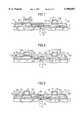
- FIG. 1illustrates a substrate with a semiconductor island
- FIG. 2illustrates the substrate after the formation of wells for the acceptance of complementary MOS transistors
- FIG. 3illustrates the substrate after formation of spacers from the second auxiliary layer
- FIG. 4illustrates the substrate after formation of first sub-regions for the source/drain regions of the p-channel transistors
- FIG. 5illustrates the substrate after removal of the spacers and formation of second sub-regions
- FIG. 6illustrates the substrate after an etching into the semiconductor island in the region of the p-channel transistor
- FIG. 7illustrates the substrate after formation of second sub-regions of the source/drain regions for the p-channel transistor by selective, in-situ-doped epitaxy
- FIG. 8illustrates the substrate after selective growth of silicon
- FIG. 9illustrates the substrate after formation of silicide layers at the surface of the source/drain regions and of the gate electrodes.
- An insulating layer 2 of, for example SiO 2 having a thickness of, for example, 400 nmis formed on a base 1 of, for example, silicon or sapphire.
- a structured silicon layer 3 having a thickness of, for example, 0 through 10 nm, an Si 1-x Ge x layer 4 with a layer thickness of, for example, 15 nm and a germanium content of, for example, 35 percent, and a strained silicon layer 5 with a layer thickness of, for example, 5 nmare formed on the insulating layer 2.
- the structured silicon layer 3, the Si 1-x Ge x layer 4 and the strained silicon layer 5together form a semiconductor island 6 (see FIG. 1).
- An SOI substrateis preferably employed for manufacturing the semiconductor island 6.
- the SOI substrateis comprised of the carrier plate 1 of silicon and the insulating layer 2 of SiO 2 and a monocrystalline silicon layer formed thereon.
- the monocrystalline layeris reduced to the desired thickness, for example by oxidation and etching with, for example, HF.
- the structured silicon layer 3is formed with the assistance of photolithographic process steps.
- the Si 1-x Ge x layer 4is grown by selective epitaxy with H 2 , SiH 2 Cl 2 , GeH 4 as process gas in the temperature range between 500° C. and 900° C. and pressure range between 1 and 760 Torr. Mechanical stresses occurring in the Si 1-x Ge x layer relax into the structured silicon layer 3 via the uncovered side faces.
- the Si 1-x Ge x layer 4 formed in the selective epitaxyis almost free of mechanical stresses.
- the strained silicon layer 5is also grown by selective epitaxy.
- H 2 , SiH 2 Cl 2is employed as process gas.
- the process temperatureis desirably between 600° C. and 800° C., and the pressure is between 1 and 760 Torr.
- the semiconductor island 6has dimensions of, for example, 2 ⁇ m ⁇ 5 ⁇ m parallel to the surface of the insulating layer 2.
- a buffer layer of Si 1-y Ge y in which the germanium percentage steadily decreases at the boundary surface to the strained silicon layer 5can be achieved.
- the buffer layeris not shown in FIG. 1.
- the buffer layerhas a thickness of, for example, 10 nm.
- the germanium content yamounts, for example, to 35 percent through 0 percent.
- a scatter oxide layer of TEOS SiO 2is first deposited to a thickness of 20 nm (not shown).
- a p-doped well 7 for the n-channel transistor and an n-doped well 8 for the p-channel transistoris formed by masked implantation (see FIG. 2).
- the implantation of the p-doped well 7is performed, for example, with a dose of 2 ⁇ 10 12 cm -2 at 7 keV.
- the implantation for forming the n-doped well 8takes place, for example, with phosphorous having a dose of 3 ⁇ 10 12 cm -2 at 15 keV.
- the final, vertical island edgesare subsequently photolithographically defined and anisotropically etched with, for example, CHF 3 /CF 4 (scatter oxide) or, respectively, HBr (Si/SiGe stack).
- the insulating layer 2is the etch stop.
- sidewall spacers 9are formed of, for example, Si 3 N 4 and the scatter oxide layer is removed (see FIG. 2).
- gate dielectric 10For forming gate dielectric 10, gate electrode 11 and cover layer 12 for the n-channel transistor and the p-channel transistor, an SiO 2 layer that, in the exemplary embodiment, is 3 nm thick is deposited by plasma deposition or by thermal oxidation at 600° C.
- the gate electrode 11can be formed with electron beam lithography or with spacer techniques.
- the gate lengthmay be, for example, to 100 nm.
- a first auxiliary layer 13 of, for example, TEOS SiO 2 or Si 3 N 4is deposited surface-wide in a layer thickness of, for example, 10 nm with essentially conformal edge coverage.
- a second auxiliary layer 14 of, for example, polysilicon having a layer thickness of, for example, 60 nmis deposited thereon. The second auxiliary layer 14 can be selectively etched relative to the first auxiliary layer.
- Spacers 140are formed in the region of the sidewalls of the gate electrodes 11 by anisotropic etching of the second auxiliary layer 14 selectively relative to the first auxiliary layer 13 with, for example, HBr.
- a first mask 15 of, for example, photoresistis formed that covers the n-doped well 8.
- An implantation with arsenic with a dose of 2 ⁇ 10 15 cm -2 at an energy of 30 keVis implemented for forming first sub-regions 16 of the source/drain regions for the n-channel transistor.
- the first mask 15is subsequently removed and a tempering step is implemented for annealing implantation damage and for the drive-in and activation of the dopant in the first sub-regions 16 of the n-channel transistor.
- the tempering stepis implemented, for example, for 60 seconds at 800° C.
- a second mask 17is produced that covers the p-doped well 7.
- First sub-regions 18 of the source/drain regions for the p-channel transistorare formed by implantation with boron at 2 ⁇ 10 15 cm -2 and 10 keV (see FIG. 4).
- the second mask 17is removed.
- the spacers 140are selectively removed relative to the first auxiliary layer 13 by wet-chemical etching with, for example, choline (see FIG. 5).
- a third mask 19 of, for example, photoresistis formed, which covers the n-doped well 8.
- Second sub-regions 20 of the source/drain regions for the n-channel transistorare formed by implantation with arsenic at 2 ⁇ 10 14 cm -2 (see FIG. 5). The depth and the dopant concentration of the second sub-regions 20 of the source/drain regions are lower than for the first sub-regions 16. The lateral dimension of the second sub-regions 20, however, is larger than that of the first sub-regions 16 since the spacers 140 were previously removed.
- a common tempering stepis implemented in order to anneal implantation damage in the formation of the first sub-regions 18 for the p-channel transistor and of the second sub-regions 20 for the n-channel transistor and in order to drive the dopant into these regions and activate it.
- the tempering steptakes place, for example, for 30 seconds at 750° C. Under these conditions, the dopant profile is prevented from coming apart, particularly in the second sub-region 20 for the n-channel transistor.
- a fourth mask 21 of, for example, photoresistis formed, which covers the p-doped well 7.
- the first auxiliary layer 13is etched in the region for the p-channel transistor by anisotropic etching with, for example, an anisotropic CHF 3 and CF 4 etching process, whereby spacers 130 at the sidewalls of the gate electrode 11 arise from the first auxiliary layer 13 (see FIG. 6).
- Depressions 22are formed in the region for the p-channel transistor to the side of the gate electrode 6 by an etching that attacks silicon selectively relative to the spacers 130.
- the etchingpreferably ensues isotropically, so that the depressions also extend under the spacers 130.
- the depressions 22exhibit a depth of, for example, 15 nm. They extend into the Si 1-x Ge x layer 4. It is advantageous in the etching of the depressions 22 to employ a germanium signal from the Si 1-x Ge x layer 4 as a stop signal.
- the etchingis done, for example, wet-chemically with choline.
- the depressions 22are filled with second sub-regions 23 of the source/drain regions for the p-channel transistor by selective, epitaxial deposition doped in situ. It is thereby advantageous to implement a low-temperature cleaning of the surfaces in situ at 750° C. by slight addition of GeH 4 or SiH 4 , whereby the natural oxide is etched off of Si surfaces.
- the in-situ-doped, selective epitaxial silicon depositiontakes place, for example, with a gas mixture of H 2 , SiH 2 Cl 2 , HCl and B 2 H 6 at 750° C. and 10 Torr.
- the process temperatureis thereby selected such that the structure and cpmposition of the structured silicon layer 3, of the Si 1-x Ge x layer 4 and of the strained silicon layer remain unmodified.
- a step-shaped dopant profile for the second sub-regions 23is generated. in a good approximation by the addition of B 2 H 6 to the process gas mixture.
- the dopantis incorporated into the crystal lattice in the second sub-regions 23 by the in-situ-doped epitaxy, so that no tempering step is required for activation of the dopants.
- the step-shaped doping profile produced in the selective epitaxytherefore defines the expanse of the second sub-regions 23 for the p-channel transistor.
- the second sub-regions 23 for the p-channel transistorhave a depth of, for example, 15 nm (see FIG. 7).
- a spacer etching with, for example, an anisotropic CHF 3 and CF 4 etching processis also implemented in the region of the n-channel transistor, whereby the first auxiliary layer 13 is etched and spacers 130 arise at the sidewalls of the gate electrode 6.
- the region of the p-channel transistorcan be covered with a further mask, which is not shown.
- Si 1-z Ge z layer 24is grown undoped.
- wet-cleaningwith, for example, an HF dip and a low-temperature cleaning at, for example, 750° C. are first implemented.
- the subsequent epitaxial deposition of Si 1-z Ge ztakes place, for example, at 650° C. and 10 Torr with a gas mixture that contains H 2 , SiH 2 Cl, HCl and GeH 4 .
- the crystal compositionis thereby selected such that the lattice constant of the Si 1-z Ge z layer 24 is essentially the same as the lattice constant of the Si 1-x Ge x layer 4, so that no further stress is built up.
- Silicide terminalsare formed after removal of the cover layer 12 from the gate electrodes 11. To that end, for example, a titanium layer is deposited and a tempering step is implemented for the formation of the titanium silicide terminals 25.
- the Si 1-z Ge z layer 24is completely consumed, so that unwanted pn-junctions do not arise anywhere.
- the titanium silicide terminals 24arise both at the surface of the first sub-regions 16, 18 and second sub-regions 20, 23 as well as on the surface of the gate electrodes 11 and on the exposed semiconductor surface between the neighboring n-channel and p-channel transistors. As a result, a source/drain region of the p-channel transistor is connected to one of the n-channel transistor. A self-aligned inverter is manufactured in this way.
- the gate electrodes 11Given short channel lengths below 150 nm, it is within the scope of the invention to manufacture the gate electrodes 11 with a T-shaped cross-section in order to improve the terminal impedance of the gate electrodes 11.
- the sidewall spacers 9 of Si 3 N 4prevent the formation of parasitic MOS transistors along the sidewalls of the semiconductor island 6.
- the sidewall spacers 9can be alternatively formed of SiO 2 .
- the gate electrode 11of at least two layers that are successively deposited and structured, and whereby a further SiO 2 spacer is formed between the two layers.
- a p-channel transistor and an n-channel transistor that are interconnected as an inverterare formed in the semiconductor island.
- the inventioncan also be applied to semiconductor islands in which only one transistor type, for example n,-channel or p-channel transistors, or only a single transistor is provided.
- the capacitance of the first sub-regions 16, 18 and second sub-regions 20, 23 of the source/drain regions to the carrier plate 1is inversely proportional to the thickness of the insulating layer 2.
- This capacitancecan be set by the thickness of the insulating layer 2.
- the insulating layer 2exhibits a thickness of, for example, 400 nm, then these capacitances are comparable to those in an MOS transistor in semiinsulating GaAs.
- capacitances comparable to Si-MOS transistors with III-V semiconductor circuitslow-field mobilities that are just about as good but, compared to Ga As, better saturation drift speeds given high fields are achieved. Given channel lengths below 100 nm, however, the saturation properties should have a greater influence on the switching times than the low-field mobilities.
Landscapes
- Metal-Oxide And Bipolar Metal-Oxide Semiconductor Integrated Circuits (AREA)
- Thin Film Transistor (AREA)
Abstract
Description
1. Field of the Invention
The present invention relates generally to the field of semiconductor devices and, more particularly, the present invention relates to an improved CMOS circuit.
Due to the structural miniaturizations in MOS technology, the properties of MOS transistors and CMOS circuits must be maintained through the micrometer range. However, in MOS transistors with channel lengths of, for example, less than 100 nm, short-channel and punch effects occur. These effects can in fact be partially compensated by an increased doping of the substrate, but the required high doping of the substrate results in, among other things, a deterioration of the charge carrier mobility in the channel. Additionally, in MOS transistors with channel lengths less than 100 nm, the subthreshold slope d In(Idrain)/d Vgate must be maximized so that, even at low operating voltages, the currents in the conductive condition and in the non-conductive condition can be clearly distinguished. Finally, in order to avoid extreme short-channel effects, flat source/drain regions must be utilized that exhibit a low specific series resistance on the order of 100 Ωμm.
2. Description of the Related Art
For increasing the charge carrier mobility, it has been proposed in the literature (see, for example, K. Rim et al., IEEE IEDM Tech. Dig., page 517 (1995) to realize n-channel and p-channel transistors in substrates that comprise strained silicon at least in the channel region of the transistors. Strained silicon is silicon whose lattice constant is increased in two spatial directions compared to unstrained silicon. Strained silicon is produced by growing silicon lattice-matched to a substrate having a higher lattice constant. Si1- Gex is suitable as such a substrate material. The high defect densities in the Si1-x Gex substrate is a problem in the manufacture of strained silicon.
It has been proposed (see A. R. Powell et al., Appl. Phys. Lett. 64, page 1856 (1994)) to grow the Si1-x Gex layer on the thinned silicon layer of an SOI substrate. Stresses in the Si1-x Gex layer relax in this case into the thinned silicon layer lying therebelow, insofar as the germanium content in the Si1-x Gex layer is less than 15 percent.
In order to manufacture very flat source/drain regions with low series resistance, Y. Mitani et al., IEEE VLSI Tech. Dig., page 91 (1996), has proposed that the source/drain regions be manufactured by etching depressions into the surface of the substrate and selective, in situ doped growth of amorphous silicon and subsequent recrystallization of the amorphous silicon. However, there are shortcomings to this design as well.
The present invention is based on the problem of providing an integrated CMOS circuit arrangement and a method for the manufacture thereof in which short-channel effects and punch effects are prevented and high charge carrier mobility is assured.
In the CMOS circuit of the present invention, the transistors are arranged in semiconductor islands that are formed on an insulating layer. Each of the semiconductor islands comprises a Si1-x Gex layer and a strained silicon layer formed thereon. The Si1-x Gex layer can be separated from the insulating layer by a silicon layer. The strained silicon layer exhibits substantially the same lattice constant as the Si1-x Gex layer. In every semiconductor island, mechanical stresses of the Si1-x Gex layer can relax as warranted via the silicon layer formed therebelow or through, for example, the thermally softened insulation material to the sides of the semiconductor islands. The Si1-x Gex layer therefore exhibits practically no defects even with germanium content above 40 percent. The use of Si1-x Gex layers with germanium content above, for example, 15 percent, has the advantage that significantly higher electron and hole mobilities are maintained in the silicon layer distorted thereon.
Given a germanium content of, for example, 40 percent, the thickness of the silicon layer can be for example, to 10 nm. The thickness of the Si1-x Gex layer can be 20 nm and that of the strained silicon layer can be 10 nm. It is within the scope of the invention to manufacture the silicon layer in the thickness range between 0 nm and approximately 20 nm, the Si1-x Gex layer in the thickness range between 10 nm and 50 nm and with germanium contentss of 20 percent through 50 percent and the strained silicon layer in the thickness range between 5 nm and 20 nm.
A conductive channel forms at the surface of the strained silicon layer in the MOS transistor in the conductive condition both for n-channel as well as for, p-channel transistors. In order to avoid the formation of buried channels at the boundary surface between the Si1-x Gex layer and the strained silicon layer, it is within the scope of the invention to provide a buffer layer between the Si1-x Gex layer and the strained silicon layer. The buffer layer contains Si1-y Gey with y≦x and the germanium portion decreasing therein. The buffer layer exhibits the lowest germanium portion at the boundary surface of the strained silicon layer.
For realizing a symmetrical CMOS circuit in which the threshold voltage of n-channel transistors is the same as the threshold voltage of the p-channel transistors, it is advantageous to provide the MOS transistors with gate electrodes that contain p+ -doped germanium. The gate electrodes can be comprised of pure polycrystalline germanium or of a mixture of polycrystalline Six Ge1-x. Polycrystalline, p+ -doped germanium has work function that is approximately in the middle of the band gap of strained silicon. Both n as well as p-surface channel MOS transistors can thus be realized with excellent characteristics. It is especially advantageous to realize a complementary MOS transistor pair in a semiconductor island that comprises a p-channel transistor and an n-channel transistor as an inverter.
The manufacture of the semiconductor islands is preferably based on an SOI substrate that comprises a silicon layer and an insulating layer arranged therebelow on a carrier wafer. The silicon layer is structured like an island, whereby the surface of the insulating layer is partially uncovered. The Si1-x Gex can be formed both by selective epitaxy on the structured silicon layer as well as by introduction of germanium into the structured silicon layer by implantation or diffusion. Selective epitaxy is advantageous in view of a defined layer thickness.
The strained silicon layer is subsequently grown by selective epitaxy. For epitaxial growth, the lattice constant from the Si1-x Gex layer is transferred into the strained silicon layer.
For flat source/drain regions, it is advantageous to respectively form the source/drain region of a first sub-region and a second sub-region. The second sub-region thus exhibits a lesser depth and lower dopant concentration than the first sub-region. The effective channel length is determined by the lateral spacing of the second sub-regions. In the literature, the term HDD profile for the first sub-regions and the term LDD profile for the second sub-regions are standard.
It is advantageous to first produce the first sub-regions, whereby spacers at the sidewalls of the gate electrode define the spacing of the first sub-regions from the gate electrode edge. After removal of these spacers, the second sub-regions of the source/drain regions are formed. Since the second sub-regions are formed after the first sub-regions, they are not subjected to the temperature loads and to the process steps for forming the first sub-regions and they can therefore be manufactured with a steeper dopant profile.
The second sub-regions for the source/drain regions of the p-channel transistors are preferably formed by etching at least into the distorted silicon layer and subsequent selective epitaxy doped in situ. Given epitaxy doped in situ, the dopant is incorporated into the epitaxially grown crystal region. A subsequent activation of the dopant is not required given epitaxy doped in situ. Nearly step-shaped dopant profiles can thus be formed.
The invention is explained in greater detail below with reference to the exemplary embodiments that are shown in the Figures.
FIG. 1 illustrates a substrate with a semiconductor island;
FIG. 2 illustrates the substrate after the formation of wells for the acceptance of complementary MOS transistors;
FIG. 3 illustrates the substrate after formation of spacers from the second auxiliary layer;
FIG. 4 illustrates the substrate after formation of first sub-regions for the source/drain regions of the p-channel transistors;
FIG. 5 illustrates the substrate after removal of the spacers and formation of second sub-regions;
FIG. 6 illustrates the substrate after an etching into the semiconductor island in the region of the p-channel transistor;
FIG. 7 illustrates the substrate after formation of second sub-regions of the source/drain regions for the p-channel transistor by selective, in-situ-doped epitaxy;
FIG. 8 illustrates the substrate after selective growth of silicon;
FIG. 9 illustrates the substrate after formation of silicide layers at the surface of the source/drain regions and of the gate electrodes.
An insulatinglayer 2 of, for example SiO2 having a thickness of, for example, 400 nm is formed on abase 1 of, for example, silicon or sapphire. A structured silicon layer 3 having a thickness of, for example, 0 through 10 nm, an Si1-x Gex layer 4 with a layer thickness of, for example, 15 nm and a germanium content of, for example, 35 percent, and a strained silicon layer 5 with a layer thickness of, for example, 5 nm are formed on the insulatinglayer 2. The structured silicon layer 3, the Si1-x Gex layer 4 and the strained silicon layer 5 together form a semiconductor island 6 (see FIG. 1).
An SOI substrate is preferably employed for manufacturing thesemiconductor island 6. The SOI substrate is comprised of thecarrier plate 1 of silicon and the insulatinglayer 2 of SiO2 and a monocrystalline silicon layer formed thereon. First, the monocrystalline layer is reduced to the desired thickness, for example by oxidation and etching with, for example, HF. Subsequently, the structured silicon layer 3 is formed with the assistance of photolithographic process steps. The Si1-x Gex layer 4 is grown by selective epitaxy with H2, SiH2 Cl2, GeH4 as process gas in the temperature range between 500° C. and 900° C. and pressure range between 1 and 760 Torr. Mechanical stresses occurring in the Si1-x Gex layer relax into the structured silicon layer 3 via the uncovered side faces. The Si1-x Gex layer 4 formed in the selective epitaxy is almost free of mechanical stresses. The strained silicon layer 5 is also grown by selective epitaxy. H2, SiH2 Cl2 is employed as process gas. The process temperature is desirably between 600° C. and 800° C., and the pressure is between 1 and 760 Torr.
Thesemiconductor island 6 has dimensions of, for example, 2 μm×5 μm parallel to the surface of the insulatinglayer 2.
By changing the process gas composition during the selective epitaxy for manufacturing the Si1-x Gex layer, a buffer layer of Si1-y Gey in which the germanium percentage steadily decreases at the boundary surface to the strained silicon layer 5 can be achieved. For the sake of clarity, the buffer layer is not shown in FIG. 1. The buffer layer has a thickness of, for example, 10 nm. The germanium content y amounts, for example, to 35 percent through 0 percent.
For manufacturing an n-channel transistor and a p-channel transistor in thesemiconductor island 6, a scatter oxide layer of TEOS SiO2 is first deposited to a thickness of 20 nm (not shown). A p-doped well 7 for the n-channel transistor and an n-doped well 8 for the p-channel transistor is formed by masked implantation (see FIG. 2). The implantation of the p-dopedwell 7 is performed, for example, with a dose of 2×1012 cm-2 at 7 keV. The implantation for forming the n-dopedwell 8 takes place, for example, with phosphorous having a dose of 3×1012 cm-2 at 15 keV.
The final, vertical island edges are subsequently photolithographically defined and anisotropically etched with, for example, CHF3 /CF4 (scatter oxide) or, respectively, HBr (Si/SiGe stack). The insulatinglayer 2 is the etch stop. After potential passivation of the sidewalls of the semiconductor island,sidewall spacers 9 are formed of, for example, Si3 N4 and the scatter oxide layer is removed (see FIG. 2).
For forminggate dielectric 10,gate electrode 11 andcover layer 12 for the n-channel transistor and the p-channel transistor, an SiO2 layer that, in the exemplary embodiment, is 3 nm thick is deposited by plasma deposition or by thermal oxidation at 600° C. A polycrystalline gate electrode layer of, for example, polycrystalline germanium or polycrystalline Si1-x Gex with x equal to 0.15 is deposited, and a cover layer of SiO2 having a thickness of, for example, 200 nm is deposited and subsequently structured with the assistance of photolithographic process steps and anisotropic etching with, for example, HBr. Alternatively, thegate electrode 11 can be formed with electron beam lithography or with spacer techniques. The gate length may be, for example, to 100 nm.
A firstauxiliary layer 13 of, for example, TEOS SiO2 or Si3 N4 is deposited surface-wide in a layer thickness of, for example, 10 nm with essentially conformal edge coverage. A secondauxiliary layer 14 of, for example, polysilicon having a layer thickness of, for example, 60 nm is deposited thereon. The secondauxiliary layer 14 can be selectively etched relative to the first auxiliary layer.
Spacers 140 (see FIG. 3) are formed in the region of the sidewalls of thegate electrodes 11 by anisotropic etching of the secondauxiliary layer 14 selectively relative to the firstauxiliary layer 13 with, for example, HBr. Afirst mask 15 of, for example, photoresist is formed that covers the n-dopedwell 8. An implantation with arsenic with a dose of 2×1015 cm-2 at an energy of 30 keV is implemented for formingfirst sub-regions 16 of the source/drain regions for the n-channel transistor. Thefirst mask 15 is subsequently removed and a tempering step is implemented for annealing implantation damage and for the drive-in and activation of the dopant in thefirst sub-regions 16 of the n-channel transistor. The tempering step is implemented, for example, for 60 seconds at 800° C.
Asecond mask 17 is produced that covers the p-dopedwell 7.First sub-regions 18 of the source/drain regions for the p-channel transistor are formed by implantation with boron at 2×1015 cm-2 and 10 keV (see FIG. 4). By employing a somewhat higher energy in the implantation for forming thefirst sub-regions 16 for the n-channel transistor and thefirst sub-regions 18 for the p-channel transistor, mechanical stresses that arise can better relax since the insulatinglayer 2 is softened given higher energy and dose of the implantation and it is easier for thesemiconductor island 6 to slide in order to relax mechanical stresses.
Thesecond mask 17 is removed. Thespacers 140 are selectively removed relative to the firstauxiliary layer 13 by wet-chemical etching with, for example, choline (see FIG. 5).
Athird mask 19 of, for example, photoresist is formed, which covers the n-dopedwell 8.Second sub-regions 20 of the source/drain regions for the n-channel transistor are formed by implantation with arsenic at 2×1014 cm-2 (see FIG. 5). The depth and the dopant concentration of thesecond sub-regions 20 of the source/drain regions are lower than for thefirst sub-regions 16. The lateral dimension of thesecond sub-regions 20, however, is larger than that of thefirst sub-regions 16 since thespacers 140 were previously removed.
After removal of thethird mask 19, a common tempering step is implemented in order to anneal implantation damage in the formation of thefirst sub-regions 18 for the p-channel transistor and of thesecond sub-regions 20 for the n-channel transistor and in order to drive the dopant into these regions and activate it. The tempering step takes place, for example, for 30 seconds at 750° C. Under these conditions, the dopant profile is prevented from coming apart, particularly in thesecond sub-region 20 for the n-channel transistor.
Afourth mask 21 of, for example, photoresist is formed, which covers the p-dopedwell 7. The firstauxiliary layer 13 is etched in the region for the p-channel transistor by anisotropic etching with, for example, an anisotropic CHF3 and CF4 etching process, wherebyspacers 130 at the sidewalls of thegate electrode 11 arise from the first auxiliary layer 13 (see FIG. 6).
After removal of thefourth mask 21 and a wet cleaning of the crystalline surfaces uncovered in the region of thedepressions 22, for example with an HF dip, thedepressions 22 are filled withsecond sub-regions 23 of the source/drain regions for the p-channel transistor by selective, epitaxial deposition doped in situ. It is thereby advantageous to implement a low-temperature cleaning of the surfaces in situ at 750° C. by slight addition of GeH4 or SiH4, whereby the natural oxide is etched off of Si surfaces.
The in-situ-doped, selective epitaxial silicon deposition takes place, for example, with a gas mixture of H2, SiH2 Cl2, HCl and B2 H6 at 750° C. and 10 Torr. The process temperature is thereby selected such that the structure and cpmposition of the structured silicon layer 3, of the Si1-x Gex layer 4 and of the strained silicon layer remain unmodified. A step-shaped dopant profile for thesecond sub-regions 23 is generated. in a good approximation by the addition of B2 H6 to the process gas mixture. The dopant is incorporated into the crystal lattice in thesecond sub-regions 23 by the in-situ-doped epitaxy, so that no tempering step is required for activation of the dopants. The step-shaped doping profile produced in the selective epitaxy therefore defines the expanse of thesecond sub-regions 23 for the p-channel transistor. Thesecond sub-regions 23 for the p-channel transistor have a depth of, for example, 15 nm (see FIG. 7).
Subsequently, a spacer etching with, for example, an anisotropic CHF3 and CF4 etching process is also implemented in the region of the n-channel transistor, whereby the firstauxiliary layer 13 is etched andspacers 130 arise at the sidewalls of thegate electrode 6. During the spacer etching in the region of the n-channel transistor, the region of the p-channel transistor can be covered with a further mask, which is not shown.
Subsequently, uncovered silicon surfaces are provided with a Si1-z Gez layer 24. The Si1-z Gez layer 24 is grown undoped. To that end, wet-cleaning with, for example, an HF dip and a low-temperature cleaning at, for example, 750° C. are first implemented. The subsequent epitaxial deposition of Si1-z Gez takes place, for example, at 650° C. and 10 Torr with a gas mixture that contains H2, SiH2 Cl, HCl and GeH4. The crystal composition is thereby selected such that the lattice constant of the Si1-z Gez layer 24 is essentially the same as the lattice constant of the Si1-x Gex layer 4, so that no further stress is built up.
Silicide terminals are formed after removal of thecover layer 12 from thegate electrodes 11. To that end, for example, a titanium layer is deposited and a tempering step is implemented for the formation of thetitanium silicide terminals 25. The Si1-z Gez layer 24 is completely consumed, so that unwanted pn-junctions do not arise anywhere. Thetitanium silicide terminals 24 arise both at the surface of thefirst sub-regions second sub-regions gate electrodes 11 and on the exposed semiconductor surface between the neighboring n-channel and p-channel transistors. As a result, a source/drain region of the p-channel transistor is connected to one of the n-channel transistor. A self-aligned inverter is manufactured in this way.
Given short channel lengths below 150 nm, it is within the scope of the invention to manufacture thegate electrodes 11 with a T-shaped cross-section in order to improve the terminal impedance of thegate electrodes 11. In this example, thesidewall spacers 9 of Si3 N4 prevent the formation of parasitic MOS transistors along the sidewalls of thesemiconductor island 6. Thesidewall spacers 9 can be alternatively formed of SiO2. In order to prevent the corners of thesemiconductor island 6 from being etched free during the structuring of thegate dielectric 10, it is within the scope of the invention in this case to manufacture thegate electrode 11 of at least two layers that are successively deposited and structured, and whereby a further SiO2 spacer is formed between the two layers.
In the exemplary embodiment, a p-channel transistor and an n-channel transistor that are interconnected as an inverter are formed in the semiconductor island. Of course, the invention can also be applied to semiconductor islands in which only one transistor type, for example n,-channel or p-channel transistors, or only a single transistor is provided.
Since thesemiconductor islands 6 are formed at the surface of the insulating layer and the capacitance of thefirst sub-regions second sub-regions carrier plate 1 is inversely proportional to the thickness of the insulatinglayer 2. This capacitance can be set by the thickness of the insulatinglayer 2. When the insulatinglayer 2 exhibits a thickness of, for example, 400 nm, then these capacitances are comparable to those in an MOS transistor in semiinsulating GaAs. In the inventive CMOS circuit arrangement, thus, capacitances comparable to Si-MOS transistors with III-V semiconductor circuits, low-field mobilities that are just about as good but, compared to Ga As, better saturation drift speeds given high fields are achieved. Given channel lengths below 100 nm, however, the saturation properties should have a greater influence on the switching times than the low-field mobilities.
The present invention is subject to many variations, modifications and changes in detail. It is intended that all matter described throughout the specification and shown in the accompanying drawings be considered illustrative only. Accordingly, it is intended that the invention be limited only by the spirit and scope of the appended claims.
Claims (6)
1. An integrated and symmetrical CMOS circuit comprising:
a plurality of semiconductor islands formed above an insulating layer, the plurality of semiconductor islands respectively comprising at least a Si1-x Gex layer, a strained, non-distorted silicon layer that exhibits substantially a same lattice constant as the Si1-x Gex layer, and at least one MOS transistor wherein the gate electrodes of the MOS transistors contain polycrystalline germanium such that n-channel transistors and p-channel transistors have substantially the same threshold voltages.
2. The CMOS circuit of claim 1, wherein a p-channel MOS transistor is provided in at least one semiconductor island and an n-channel MOS transistor is provided in at least one semiconductor island.
3. A CMOS circuit according to claim 1, wherein a silicon layer is formed between the Si1-x Gex layer and the insulating layer.
4. A CMOS circuit according to claim 3, wherein the structured silicon layer has a thickness of less than 20 nm; and
the Si1-x Gex layer has a thickness of from 10 nm to 50 nm and a germanium composition of between 20 percent and 50 percent; and
wherein the strained silicon layer has a thickness of between 5 nm and 20 nm.
5. A CMOS circuit according to claim 4, wherein a buffer layer that contains Siy-1 Gey and in which the germanium content decreases is formed between the Si1-x Gex layer and the strained silicon layer.
6. A CMOS circuit according to claim 1, wherein at least one p-channel transistor and one n-channel transistor are formed in at least one semiconductor island.
Applications Claiming Priority (2)
| Application Number | Priority Date | Filing Date | Title |
|---|---|---|---|
| DE19639874 | 1996-09-27 | ||
| DE19639874 | 1996-09-27 |
Publications (1)
| Publication Number | Publication Date |
|---|---|
| US5998807Atrue US5998807A (en) | 1999-12-07 |
Family
ID=7807153
Family Applications (1)
| Application Number | Title | Priority Date | Filing Date |
|---|---|---|---|
| US08/925,672Expired - LifetimeUS5998807A (en) | 1996-09-27 | 1997-09-09 | Integrated CMOS circuit arrangement and method for the manufacture thereof |
Country Status (6)
| Country | Link |
|---|---|
| US (1) | US5998807A (en) |
| EP (1) | EP0838858B1 (en) |
| JP (1) | JP4034387B2 (en) |
| KR (1) | KR100440508B1 (en) |
| DE (1) | DE59707274D1 (en) |
| TW (1) | TW344140B (en) |
Cited By (78)
| Publication number | Priority date | Publication date | Assignee | Title |
|---|---|---|---|---|
| US20020022366A1 (en)* | 2000-05-11 | 2002-02-21 | International Business Machines Corporation | Self-aligned silicide (salicide) process for low resistivity contacts to thin film silicon-on-insulator and bulk MOSFETS and for shallow Junctions |
| US20020042183A1 (en)* | 2000-02-10 | 2002-04-11 | Chan Kevin K. | Two-step MOSFET gate formation for high-density devices |
| US6380590B1 (en) | 2001-02-22 | 2002-04-30 | Advanced Micro Devices, Inc. | SOI chip having multiple threshold voltage MOSFETs by using multiple channel materials and method of fabricating same |
| US6410371B1 (en) | 2001-02-26 | 2002-06-25 | Advanced Micro Devices, Inc. | Method of fabrication of semiconductor-on-insulator (SOI) wafer having a Si/SiGe/Si active layer |
| US6413829B1 (en)* | 2001-06-01 | 2002-07-02 | Advanced Micro Devices, Inc. | Field effect transistor in SOI technology with schottky-contact extensions |
| US20020090772A1 (en)* | 2000-12-11 | 2002-07-11 | Seiko Epson Corporation | Method for manufacturing semiconductor lamination, method for manufacturing lamination, semiconductor device, and electronic equipment |
| US20020123167A1 (en)* | 2001-03-02 | 2002-09-05 | Fitzgerald Eugene A. | Relaxed silicon germanium platform for high speed CMOS electronics and high speed analog circuits |
| US20020149038A1 (en)* | 2001-04-04 | 2002-10-17 | Yoshifumi Yoshida | Semiconductor device |
| US6469335B2 (en)* | 2000-03-28 | 2002-10-22 | Infineon Technologies Ag | Semiconductor memory having a memory cell array |
| US6495402B1 (en) | 2001-02-06 | 2002-12-17 | Advanced Micro Devices, Inc. | Semiconductor-on-insulator (SOI) device having source/drain silicon-germanium regions and method of manufacture |
| US20020197803A1 (en)* | 2001-06-21 | 2002-12-26 | Amberwave Systems Corporation | Enhancement of p-type metal-oxide-semiconductor field effect transistors |
| US20030013323A1 (en)* | 2001-06-14 | 2003-01-16 | Richard Hammond | Method of selective removal of SiGe alloys |
| US20030057439A1 (en)* | 2001-08-09 | 2003-03-27 | Fitzgerald Eugene A. | Dual layer CMOS devices |
| US6544854B1 (en)* | 2000-11-28 | 2003-04-08 | Lsi Logic Corporation | Silicon germanium CMOS channel |
| US20030068883A1 (en)* | 2000-11-15 | 2003-04-10 | International Business Machines Corporation | Self-aligned silicide (salicide) process for strained silicon MOSFET on SiGe and structure formed thereby |
| US6555839B2 (en) | 2000-05-26 | 2003-04-29 | Amberwave Systems Corporation | Buried channel strained silicon FET using a supply layer created through ion implantation |
| US6573126B2 (en) | 2000-08-16 | 2003-06-03 | Massachusetts Institute Of Technology | Process for producing semiconductor article using graded epitaxial growth |
| US6593641B1 (en) | 2001-03-02 | 2003-07-15 | Amberwave Systems Corporation | Relaxed silicon germanium platform for high speed CMOS electronics and high speed analog circuits |
| US6602613B1 (en) | 2000-01-20 | 2003-08-05 | Amberwave Systems Corporation | Heterointegration of materials using deposition and bonding |
| WO2003028106A3 (en)* | 2001-09-24 | 2003-11-13 | Amberwave Systems Corp | Rf circuits including transistors having strained material layers |
| US6649480B2 (en) | 2000-12-04 | 2003-11-18 | Amberwave Systems Corporation | Method of fabricating CMOS inverter and integrated circuits utilizing strained silicon surface channel MOSFETs |
| WO2002047168A3 (en)* | 2000-12-04 | 2003-12-31 | Amberwave Systems Corp | Cmos inverter circuits utilizing strained silicon surface channel mosfets |
| US6682965B1 (en)* | 1997-03-27 | 2004-01-27 | Sony Corporation | Method of forming n-and p- channel field effect transistors on the same silicon layer having a strain effect |
| US20040026765A1 (en)* | 2002-06-07 | 2004-02-12 | Amberwave Systems Corporation | Semiconductor devices having strained dual channel layers |
| US6696328B2 (en) | 2002-05-23 | 2004-02-24 | Samsung Electronics Co., Ltd. | CMOS gate electrode using selective growth and a fabrication method thereof |
| US6703688B1 (en) | 2001-03-02 | 2004-03-09 | Amberwave Systems Corporation | Relaxed silicon germanium platform for high speed CMOS electronics and high speed analog circuits |
| US20040045499A1 (en)* | 2002-06-10 | 2004-03-11 | Amberwave Systems Corporation | Source and drain elements |
| US6713819B1 (en)* | 2002-04-08 | 2004-03-30 | Advanced Micro Devices, Inc. | SOI MOSFET having amorphized source drain and method of fabrication |
| US6724008B2 (en) | 2001-03-02 | 2004-04-20 | Amberwave Systems Corporation | Relaxed silicon germanium platform for high speed CMOS electronics and high speed analog circuits |
| US6723661B2 (en) | 2001-03-02 | 2004-04-20 | Amberwave Systems Corporation | Relaxed silicon germanium platform for high speed CMOS electronics and high speed analog circuits |
| US6727550B2 (en)* | 2001-07-06 | 2004-04-27 | Kabushiki Kaisha Toshiba | Integrated circuit device |
| US6730551B2 (en) | 2001-08-06 | 2004-05-04 | Massachusetts Institute Of Technology | Formation of planar strained layers |
| US6743689B1 (en)* | 2003-01-14 | 2004-06-01 | Advanced Micro Devices, Inc. | Method of fabrication SOI devices with accurately defined monocrystalline source/drain extensions |
| US20040108598A1 (en)* | 2001-04-18 | 2004-06-10 | International Business Machines Corporation | Self-aligned silicide process for silicon sidewall source and drain contacts and structure formed thereby |
| US6750130B1 (en) | 2000-01-20 | 2004-06-15 | Amberwave Systems Corporation | Heterointegration of materials using deposition and bonding |
| WO2004038802A3 (en)* | 2002-10-18 | 2004-09-10 | Infineon Technologies Ag | Integrated circuit arrangement comprising capacitors and preferably planar transistors, and production method |
| GB2400729A (en)* | 2000-01-07 | 2004-10-20 | Samsung Electronics Co Ltd | CMOS integrated circuit devices and substrates having buried silicon germanium layers therein and methods of making same |
| US6864115B2 (en) | 2000-01-20 | 2005-03-08 | Amberwave Systems Corporation | Low threading dislocation density relaxed mismatched epilayers without high temperature growth |
| US20050070056A1 (en)* | 2003-09-25 | 2005-03-31 | Chun-Li Liu | SOI template layer |
| US6876010B1 (en) | 1997-06-24 | 2005-04-05 | Massachusetts Institute Of Technology | Controlling threading dislocation densities in Ge on Si using graded GeSi layers and planarization |
| US6900103B2 (en) | 2001-03-02 | 2005-05-31 | Amberwave Systems Corporation | Relaxed silicon germanium platform for high speed CMOS electronics and high speed analog circuits |
| US6905923B1 (en)* | 2003-07-15 | 2005-06-14 | Advanced Micro Devices, Inc. | Offset spacer process for forming N-type transistors |
| US20050151163A1 (en)* | 2004-01-06 | 2005-07-14 | Kabushiki Kaisha Toshiba | Semiconductor device and manufacturing method thereof |
| US20050156156A1 (en)* | 2002-12-13 | 2005-07-21 | Taiwan Semiconductor Manufacturing Company, Ltd. | Method of fabricating a non-floating body device with enhanced performance |
| US6940089B2 (en) | 2001-04-04 | 2005-09-06 | Massachusetts Institute Of Technology | Semiconductor device structure |
| US20050194585A1 (en)* | 2004-03-05 | 2005-09-08 | Kabushiki Kaisha Toshiba | Field effect transistor and a method for manufacturing the same |
| US20050202603A1 (en)* | 2002-11-20 | 2005-09-15 | Renesas Technology Corp. | Semiconductor device including gate electrode for applying tensile stress to silicon substrate, and method of manufacturing the same |
| US20050236687A1 (en)* | 2004-04-22 | 2005-10-27 | International Business Machines Corporation | Strained silicon CMOS on hybrid crystal orientations |
| US20050260809A1 (en)* | 2002-07-29 | 2005-11-24 | Tsutomu Tezuka | Semiconductor device manufacturing method |
| US6982474B2 (en) | 2002-06-25 | 2006-01-03 | Amberwave Systems Corporation | Reacted conductive gate electrodes |
| US6995430B2 (en) | 2002-06-07 | 2006-02-07 | Amberwave Systems Corporation | Strained-semiconductor-on-insulator device structures |
| US20060040433A1 (en)* | 2004-08-17 | 2006-02-23 | Sadaka Mariam G | Graded semiconductor layer |
| US20060038200A1 (en)* | 2004-08-20 | 2006-02-23 | Samsung Electronics Co., Ltd. | Transistors having reinforcement layer patterns and methods of forming the same |
| US7049627B2 (en) | 2002-08-23 | 2006-05-23 | Amberwave Systems Corporation | Semiconductor heterostructures and related methods |
| US7060632B2 (en) | 2002-03-14 | 2006-06-13 | Amberwave Systems Corporation | Methods for fabricating strained layers on semiconductor substrates |
| US7074623B2 (en) | 2002-06-07 | 2006-07-11 | Amberwave Systems Corporation | Methods of forming strained-semiconductor-on-insulator finFET device structures |
| US20060228851A1 (en)* | 2005-03-30 | 2006-10-12 | Sadaka Mariam G | Method of making a dual strained channel semiconductor device |
| US7138649B2 (en)* | 2001-08-09 | 2006-11-21 | Amberwave Systems Corporation | Dual-channel CMOS transistors with differentially strained channels |
| US20070082470A1 (en)* | 2000-08-07 | 2007-04-12 | Amberwave System Corporation | Gate technology for strained surface channel and strained buried channel MOSFET devices |
| US7217608B1 (en)* | 2001-12-17 | 2007-05-15 | Advanced Micro Devices, Inc. | CMOS with strained silicon channel NMOS and silicon germanium channel PMOS |
| US20070117297A1 (en)* | 2000-01-07 | 2007-05-24 | Geum-Jong Bae | CMOS integrated circuit devices and substrates having buried silicon germanium layers therein and method of forming same |
| US7227176B2 (en) | 1998-04-10 | 2007-06-05 | Massachusetts Institute Of Technology | Etch stop layer system |
| US20070131969A1 (en)* | 2005-11-30 | 2007-06-14 | Kabushiki Kaisha Toshiba | Semiconductor device and method of manufacturing the same |
| US20070212857A1 (en)* | 2004-10-08 | 2007-09-13 | Anderson Brent A | Integrated Circuit With Bulk and SOI Devices Connected with an Epitaxial Region |
| US7301180B2 (en) | 2001-06-18 | 2007-11-27 | Massachusetts Institute Of Technology | Structure and method for a high-speed semiconductor device having a Ge channel layer |
| US7307273B2 (en) | 2002-06-07 | 2007-12-11 | Amberwave Systems Corporation | Control of strain in device layers by selective relaxation |
| US20070287244A1 (en)* | 2006-04-26 | 2007-12-13 | Applied Materials, Inc., A Delaware Corporation | ALTERNATIVE INTEGRATION SCHEME FOR CMOS S/D SiGe PROCESS |
| US7332417B2 (en) | 2003-01-27 | 2008-02-19 | Amberwave Systems Corporation | Semiconductor structures with structural homogeneity |
| US7335545B2 (en) | 2002-06-07 | 2008-02-26 | Amberwave Systems Corporation | Control of strain in device layers by prevention of relaxation |
| CN100380633C (en)* | 2004-07-02 | 2008-04-09 | 国际商业机器公司 | Method of forming semiconductor structure and semiconductor structure |
| US7393733B2 (en) | 2004-12-01 | 2008-07-01 | Amberwave Systems Corporation | Methods of forming hybrid fin field-effect transistor structures |
| US7504704B2 (en) | 2003-03-07 | 2009-03-17 | Amberwave Systems Corporation | Shallow trench isolation process |
| US7594967B2 (en) | 2002-08-30 | 2009-09-29 | Amberwave Systems Corporation | Reduction of dislocation pile-up formation during relaxed lattice-mismatched epitaxy |
| US7615829B2 (en)* | 2002-06-07 | 2009-11-10 | Amberwave Systems Corporation | Elevated source and drain elements for strained-channel heterojuntion field-effect transistors |
| US20100197084A1 (en)* | 2009-02-04 | 2010-08-05 | Hynix Semiconductor Inc. | Method for manufacturing semiconductor device |
| US7776697B2 (en) | 2001-09-21 | 2010-08-17 | Taiwan Semiconductor Manufacturing Company, Ltd. | Semiconductor structures employing strained material layers with defined impurity gradients and methods for fabricating same |
| US8748292B2 (en) | 2002-06-07 | 2014-06-10 | Taiwan Semiconductor Manufacturing Company, Ltd. | Methods of forming strained-semiconductor-on-insulator device structures |
| EP3331011A1 (en)* | 2016-12-02 | 2018-06-06 | InnoLux Corporation | Display device |
Families Citing this family (16)
| Publication number | Priority date | Publication date | Assignee | Title |
|---|---|---|---|---|
| DE19845066C2 (en)* | 1998-09-30 | 2000-08-03 | Siemens Ag | Integrated circuit arrangement and method for its production |
| JP4521542B2 (en)* | 1999-03-30 | 2010-08-11 | ルネサスエレクトロニクス株式会社 | Semiconductor device and semiconductor substrate |
| JP2002043576A (en)* | 2000-07-24 | 2002-02-08 | Univ Tohoku | Semiconductor device |
| JP3998408B2 (en)* | 2000-09-29 | 2007-10-24 | 株式会社東芝 | Semiconductor device and manufacturing method thereof |
| KR100516673B1 (en)* | 2000-12-11 | 2005-09-22 | 주식회사 하이닉스반도체 | A method for manufacturing a semiconductor device |
| KR100495023B1 (en)* | 2000-12-28 | 2005-06-14 | 가부시끼가이샤 도시바 | A semiconductor device and manufacturing method thereof |
| DE10214066B4 (en)* | 2002-03-28 | 2007-02-01 | Advanced Micro Devices, Inc., Sunnyvale | Semiconductor device having a retrograde doping profile in a channel region and method of making the same |
| CN100399576C (en) | 2002-03-28 | 2008-07-02 | 先进微装置公司 | Semiconductor component with degenerate doping profile in the channel region and method for producing the semiconductor component |
| EP1593145A2 (en)* | 2002-10-30 | 2005-11-09 | Amberwave Systems Corporation | Methods for preserving strained semiconductor layers during oxide layer formation |
| US6891192B2 (en)* | 2003-08-04 | 2005-05-10 | International Business Machines Corporation | Structure and method of making strained semiconductor CMOS transistors having lattice-mismatched semiconductor regions underlying source and drain regions |
| US6906360B2 (en)* | 2003-09-10 | 2005-06-14 | International Business Machines Corporation | Structure and method of making strained channel CMOS transistors having lattice-mismatched epitaxial extension and source and drain regions |
| US7303949B2 (en) | 2003-10-20 | 2007-12-04 | International Business Machines Corporation | High performance stress-enhanced MOSFETs using Si:C and SiGe epitaxial source/drain and method of manufacture |
| JP2005244187A (en)* | 2004-01-30 | 2005-09-08 | Toshiba Ceramics Co Ltd | Strained silicon wafer and manufacturing method thereof |
| JP4177775B2 (en) | 2004-03-16 | 2008-11-05 | 株式会社東芝 | Semiconductor substrate, manufacturing method thereof, and semiconductor device |
| JP2006287006A (en)* | 2005-04-01 | 2006-10-19 | Renesas Technology Corp | Semiconductor substrate, semiconductor device, and its manufacturing method |
| KR100760912B1 (en)* | 2005-12-29 | 2007-09-21 | 동부일렉트로닉스 주식회사 | Semiconductor device and manufacturing method thereof |
Citations (10)
| Publication number | Priority date | Publication date | Assignee | Title |
|---|---|---|---|---|
| EP0331811A2 (en)* | 1987-12-18 | 1989-09-13 | Fujitsu Limited | Semiconductor devices with silicon-on-insulator structures |
| EP0469790A1 (en)* | 1990-08-02 | 1992-02-05 | AT&T Corp. | Semiconductor devices with low dislocation defects and method for making same |
| EP0480446A2 (en)* | 1990-10-12 | 1992-04-15 | Texas Instruments Incorporated | Method of fabricating a high-performance insulated-gate-field-effect transistor and transistor fabricated by it |
| EP0587520A1 (en)* | 1992-08-10 | 1994-03-16 | International Business Machines Corporation | A SiGe thin film or SOI MOSFET and method for making the same |
| EP0651435A1 (en)* | 1993-09-29 | 1995-05-03 | Fuji Electric Co. Ltd. | Semiconductor device comprising a SIPOS field plate and its manufacturing method |
| JPH07142742A (en)* | 1993-08-30 | 1995-06-02 | Sharp Corp | Method for forming GeSi / Si / SiO2 heterostructure, and SIMOX device and integrated circuit having the structure |
| EP0683522A2 (en)* | 1994-05-20 | 1995-11-22 | International Business Machines Corporation | CMOS with strained Si/SiGe layers |
| US5572046A (en)* | 1993-06-30 | 1996-11-05 | Semiconductor Energy Laboratory Co., Ltd. | Semiconductor device having at least two thin film transistors |
| US5619057A (en)* | 1994-01-19 | 1997-04-08 | Sony Corporation | Complex film overlying a substrate with defined work function |
| US5656859A (en)* | 1995-03-27 | 1997-08-12 | Kabushiki Kaisha Toshiba | Semiconductor device |
Family Cites Families (1)
| Publication number | Priority date | Publication date | Assignee | Title |
|---|---|---|---|---|
| US5461243A (en)* | 1993-10-29 | 1995-10-24 | International Business Machines Corporation | Substrate for tensilely strained semiconductor |
- 1997
- 1997-08-08EPEP97113774Apatent/EP0838858B1/ennot_activeExpired - Lifetime
- 1997-08-08DEDE59707274Tpatent/DE59707274D1/ennot_activeExpired - Lifetime
- 1997-09-09USUS08/925,672patent/US5998807A/ennot_activeExpired - Lifetime
- 1997-09-24JPJP27639497Apatent/JP4034387B2/ennot_activeExpired - Fee Related
- 1997-09-26TWTW086114049Apatent/TW344140B/ennot_activeIP Right Cessation
- 1997-09-26KRKR1019970048906Apatent/KR100440508B1/ennot_activeExpired - Fee Related
Patent Citations (11)
| Publication number | Priority date | Publication date | Assignee | Title |
|---|---|---|---|---|
| EP0331811A2 (en)* | 1987-12-18 | 1989-09-13 | Fujitsu Limited | Semiconductor devices with silicon-on-insulator structures |
| EP0469790A1 (en)* | 1990-08-02 | 1992-02-05 | AT&T Corp. | Semiconductor devices with low dislocation defects and method for making same |
| EP0480446A2 (en)* | 1990-10-12 | 1992-04-15 | Texas Instruments Incorporated | Method of fabricating a high-performance insulated-gate-field-effect transistor and transistor fabricated by it |
| EP0587520A1 (en)* | 1992-08-10 | 1994-03-16 | International Business Machines Corporation | A SiGe thin film or SOI MOSFET and method for making the same |
| US5461250A (en)* | 1992-08-10 | 1995-10-24 | International Business Machines Corporation | SiGe thin film or SOI MOSFET and method for making the same |
| US5572046A (en)* | 1993-06-30 | 1996-11-05 | Semiconductor Energy Laboratory Co., Ltd. | Semiconductor device having at least two thin film transistors |
| JPH07142742A (en)* | 1993-08-30 | 1995-06-02 | Sharp Corp | Method for forming GeSi / Si / SiO2 heterostructure, and SIMOX device and integrated circuit having the structure |
| EP0651435A1 (en)* | 1993-09-29 | 1995-05-03 | Fuji Electric Co. Ltd. | Semiconductor device comprising a SIPOS field plate and its manufacturing method |
| US5619057A (en)* | 1994-01-19 | 1997-04-08 | Sony Corporation | Complex film overlying a substrate with defined work function |
| EP0683522A2 (en)* | 1994-05-20 | 1995-11-22 | International Business Machines Corporation | CMOS with strained Si/SiGe layers |
| US5656859A (en)* | 1995-03-27 | 1997-08-12 | Kabushiki Kaisha Toshiba | Semiconductor device |
Non-Patent Citations (16)
| Title |
|---|
| 1996 Symposium On VLSI Technology Digest of Technical Paper, Y. Mitani et al., "Buried Source and Drain (BSD) Structure for Ultra-shallow Junction Using Selective Deposition of Highly Doped Amorphous Silicon", 1996. |
| 1996 Symposium On VLSI Technology Digest of Technical Paper, Y. Mitani et al., Buried Source and Drain (BSD) Structure for Ultra shallow Junction Using Selective Deposition of Highly Doped Amorphous Silicon , 1996.* |
| Appl. Phys. Lett. 64, Apr. 4, 1994, "New Approach to the Growth of Low Disclocation Relaxed SiGe Material", A.R. Powell et al., p. 1856-1858. |
| Appl. Phys. Lett. 64, Apr. 4, 1994, New Approach to the Growth of Low Disclocation Relaxed SiGe Material , A.R. Powell et al., p. 1856 1858.* |
| IBM Technical Disclosure Bulletin, "Planar Fully-Integrated Bulk/SOI SiGe CMOS Fabrication Process", vol. 34, No. 10A, Mar. 1992, pp. 128-129. |
| IBM Technical Disclosure Bulletin, Planar Fully Integrated Bulk/SOI SiGe CMOS Fabrication Process , vol. 34, No. 10A, Mar. 1992, pp. 128 129.* |
| IEDM, Enhanced Hole Mobilities in Surface channel Strained Si p Mosfets, R. Kim eta 1., XP 002073202, 1995.* |
| IEDM, Enhanced Hole Mobilities in Surface-channel Strained-Si p-Mosfets, R. Kim eta 1., XP-002073202, 1995. |
| IEEE Electron Device Letters, High Mobility GeSi PMOS on Simox, No. 11, D.K. Nayak et al., Nov. 1993.* |
| IEEE Electron Device Letters, High-Mobility GeSi PMOS on Simox, No. 11, D.K. Nayak et al., Nov. 1993. |
| IEEE Electron Device Letters, vol. 15, No. 3, Mar. 1994, "Electron Mobility Electron Enhancement in Strained-Si N-type Metal-Oxide-Semiconductor Field-Effect Transistors", J. Wesler et al. |
| IEEE Electron Device Letters, vol. 15, No. 3, Mar. 1994, Electron Mobility Electron Enhancement in Strained Si N type Metal Oxide Semiconductor Field Effect Transistors , J. Wesler et al.* |
| IEEE IEDM Tech. Dig. S., R. Kim et al., "Enhanced Hole Mobilities in Surface-channel Strained-Si p-MOSFETs", p. 20.3.1-20.3.4. |
| IEEE IEDM Tech. Dig. S., R. Kim et al., Enhanced Hole Mobilities in Surface channel Strained Si p MOSFETs , p. 20.3.1 20.3.4.* |
| Journal Of Vacuum Science And Technology, "The effect of substrate growth area on misfit threading disclocation densities in mismatched heterostructures", E. Fitzgerald, No. 4, Jul./Aug. 1989. |
| Journal Of Vacuum Science And Technology, The effect of substrate growth area on misfit threading disclocation densities in mismatched heterostructures , E. Fitzgerald, No. 4, Jul./Aug. 1989.* |
Cited By (178)
| Publication number | Priority date | Publication date | Assignee | Title |
|---|---|---|---|---|
| US7355214B2 (en) | 1997-03-27 | 2008-04-08 | Sony Corporation | Field effect transistor and fabrication thereof, semiconductor device and fabrication thereof, logic circuit including the semiconductor device, and semiconductor substrate |
| US6682965B1 (en)* | 1997-03-27 | 2004-01-27 | Sony Corporation | Method of forming n-and p- channel field effect transistors on the same silicon layer having a strain effect |
| US20040135210A1 (en)* | 1997-03-27 | 2004-07-15 | Takashi Noguchi | Field effect transistor and fabrication thereof, semiconductor device and fabrication thereof, logic circuit including the semiconductor device, and semiconductor substrate |
| US7851289B2 (en) | 1997-03-27 | 2010-12-14 | Sony Corporation | Method of forming N-and P- channel field effect transistors on the same silicon layer having a strain effect |
| US20080176367A1 (en)* | 1997-03-27 | 2008-07-24 | Sony Corporation | Field effect transistor and fabrication thereof, semiconductor device and fabrication thereof, logic circuit including the semiconductor device, and semiconductor substrate |
| US7250359B2 (en) | 1997-06-24 | 2007-07-31 | Massachusetts Institute Of Technology | Controlling threading dislocation densities in Ge on Si using graded GeSi layers and planarization |
| US7081410B2 (en) | 1997-06-24 | 2006-07-25 | Massachusetts Institute Of Technology | Controlling threading dislocation densities in Ge on Si using graded GeSi layers and planarization |
| US6876010B1 (en) | 1997-06-24 | 2005-04-05 | Massachusetts Institute Of Technology | Controlling threading dislocation densities in Ge on Si using graded GeSi layers and planarization |
| US7227176B2 (en) | 1998-04-10 | 2007-06-05 | Massachusetts Institute Of Technology | Etch stop layer system |
| GB2400729A (en)* | 2000-01-07 | 2004-10-20 | Samsung Electronics Co Ltd | CMOS integrated circuit devices and substrates having buried silicon germanium layers therein and methods of making same |
| GB2400729B (en)* | 2000-01-07 | 2004-12-08 | Samsung Electronics Co Ltd | CMOS integrated circuit devices and substrates having buried silicon germanium layers therein and methods of forming same |
| US20070117297A1 (en)* | 2000-01-07 | 2007-05-24 | Geum-Jong Bae | CMOS integrated circuit devices and substrates having buried silicon germanium layers therein and method of forming same |
| US7642140B2 (en)* | 2000-01-07 | 2010-01-05 | Samsung Electronics Co., Ltd. | CMOS integrated circuit devices and substrates having buried silicon germanium layers therein and method of forming same |
| US6703144B2 (en) | 2000-01-20 | 2004-03-09 | Amberwave Systems Corporation | Heterointegration of materials using deposition and bonding |
| US6750130B1 (en) | 2000-01-20 | 2004-06-15 | Amberwave Systems Corporation | Heterointegration of materials using deposition and bonding |
| US6864115B2 (en) | 2000-01-20 | 2005-03-08 | Amberwave Systems Corporation | Low threading dislocation density relaxed mismatched epilayers without high temperature growth |
| US6602613B1 (en) | 2000-01-20 | 2003-08-05 | Amberwave Systems Corporation | Heterointegration of materials using deposition and bonding |
| US20020042183A1 (en)* | 2000-02-10 | 2002-04-11 | Chan Kevin K. | Two-step MOSFET gate formation for high-density devices |
| US6469335B2 (en)* | 2000-03-28 | 2002-10-22 | Infineon Technologies Ag | Semiconductor memory having a memory cell array |
| US20020031909A1 (en)* | 2000-05-11 | 2002-03-14 | Cyril Cabral | Self-aligned silicone process for low resistivity contacts to thin film silicon-on-insulator mosfets |
| US20020022366A1 (en)* | 2000-05-11 | 2002-02-21 | International Business Machines Corporation | Self-aligned silicide (salicide) process for low resistivity contacts to thin film silicon-on-insulator and bulk MOSFETS and for shallow Junctions |
| US20060043484A1 (en)* | 2000-05-11 | 2006-03-02 | International Business Machines Corporation | Self-aligned silicide (salicide) process for low resistivity contacts to thin film silicon-on-insulator and bulk mosfets and for shallow junctions |
| US6987050B2 (en) | 2000-05-11 | 2006-01-17 | International Business Machines Corporation | Self-aligned silicide (salicide) process for low resistivity contacts to thin film silicon-on-insulator and bulk MOSFETS and for shallow junctions |
| US6555839B2 (en) | 2000-05-26 | 2003-04-29 | Amberwave Systems Corporation | Buried channel strained silicon FET using a supply layer created through ion implantation |
| US6969875B2 (en)* | 2000-05-26 | 2005-11-29 | Amberwave Systems Corporation | Buried channel strained silicon FET using a supply layer created through ion implantation |
| US20070082470A1 (en)* | 2000-08-07 | 2007-04-12 | Amberwave System Corporation | Gate technology for strained surface channel and strained buried channel MOSFET devices |
| US6713326B2 (en) | 2000-08-16 | 2004-03-30 | Masachusetts Institute Of Technology | Process for producing semiconductor article using graded epitaxial growth |
| US6921914B2 (en) | 2000-08-16 | 2005-07-26 | Massachusetts Institute Of Technology | Process for producing semiconductor article using graded epitaxial growth |
| US6737670B2 (en) | 2000-08-16 | 2004-05-18 | Massachusetts Institute Of Technology | Semiconductor substrate structure |
| US6573126B2 (en) | 2000-08-16 | 2003-06-03 | Massachusetts Institute Of Technology | Process for producing semiconductor article using graded epitaxial growth |
| US20030068883A1 (en)* | 2000-11-15 | 2003-04-10 | International Business Machines Corporation | Self-aligned silicide (salicide) process for strained silicon MOSFET on SiGe and structure formed thereby |
| US6544854B1 (en)* | 2000-11-28 | 2003-04-08 | Lsi Logic Corporation | Silicon germanium CMOS channel |
| US20100022073A1 (en)* | 2000-12-04 | 2010-01-28 | Fitzgerald Eugene A | Method of Fabricating CMOS Inverter and Integrated Circuits Utilizing Strained Silicon Surface Channel MOSFETS |
| WO2002047168A3 (en)* | 2000-12-04 | 2003-12-31 | Amberwave Systems Corp | Cmos inverter circuits utilizing strained silicon surface channel mosfets |
| US6881632B2 (en) | 2000-12-04 | 2005-04-19 | Amberwave Systems Corporation | Method of fabricating CMOS inverter and integrated circuits utilizing strained surface channel MOSFETS |
| US6649480B2 (en) | 2000-12-04 | 2003-11-18 | Amberwave Systems Corporation | Method of fabricating CMOS inverter and integrated circuits utilizing strained silicon surface channel MOSFETs |
| US9219065B2 (en)* | 2000-12-04 | 2015-12-22 | Taiwan Semiconductor Manufacturing Company, Ltd. | Method of fabricating CMOS inverter and integrated circuits utilizing strained silicon surface channel MOSFETS |
| US20020090772A1 (en)* | 2000-12-11 | 2002-07-11 | Seiko Epson Corporation | Method for manufacturing semiconductor lamination, method for manufacturing lamination, semiconductor device, and electronic equipment |
| US6787852B1 (en) | 2001-02-06 | 2004-09-07 | Advanced Micro Devices, Inc. | Semiconductor-on-insulator (SOI) device having source/drain silicon-germanium regions |
| US6495402B1 (en) | 2001-02-06 | 2002-12-17 | Advanced Micro Devices, Inc. | Semiconductor-on-insulator (SOI) device having source/drain silicon-germanium regions and method of manufacture |
| US6380590B1 (en) | 2001-02-22 | 2002-04-30 | Advanced Micro Devices, Inc. | SOI chip having multiple threshold voltage MOSFETs by using multiple channel materials and method of fabricating same |
| US6765227B1 (en)* | 2001-02-26 | 2004-07-20 | Advanced Micro Devices, Inc. | Semiconductor-on-insulator (SOI) wafer having a Si/SiGe/Si active layer and method of fabrication using wafer bonding |
| US6410371B1 (en) | 2001-02-26 | 2002-06-25 | Advanced Micro Devices, Inc. | Method of fabrication of semiconductor-on-insulator (SOI) wafer having a Si/SiGe/Si active layer |
| US6703688B1 (en) | 2001-03-02 | 2004-03-09 | Amberwave Systems Corporation | Relaxed silicon germanium platform for high speed CMOS electronics and high speed analog circuits |
| US6900103B2 (en) | 2001-03-02 | 2005-05-31 | Amberwave Systems Corporation | Relaxed silicon germanium platform for high speed CMOS electronics and high speed analog circuits |
| US6593641B1 (en) | 2001-03-02 | 2003-07-15 | Amberwave Systems Corporation | Relaxed silicon germanium platform for high speed CMOS electronics and high speed analog circuits |
| US6724008B2 (en) | 2001-03-02 | 2004-04-20 | Amberwave Systems Corporation | Relaxed silicon germanium platform for high speed CMOS electronics and high speed analog circuits |
| US6830976B2 (en) | 2001-03-02 | 2004-12-14 | Amberwave Systems Corproation | Relaxed silicon germanium platform for high speed CMOS electronics and high speed analog circuits |
| US6723661B2 (en) | 2001-03-02 | 2004-04-20 | Amberwave Systems Corporation | Relaxed silicon germanium platform for high speed CMOS electronics and high speed analog circuits |
| US7501351B2 (en) | 2001-03-02 | 2009-03-10 | Amberwave Systems Corporation | Relaxed SiGe platform for high speed CMOS electronics and high speed analog circuits |
| US7256142B2 (en) | 2001-03-02 | 2007-08-14 | Amberwave Systems Corporation | Relaxed SiGe platform for high speed CMOS electronics and high speed analog circuits |
| US20020123167A1 (en)* | 2001-03-02 | 2002-09-05 | Fitzgerald Eugene A. | Relaxed silicon germanium platform for high speed CMOS electronics and high speed analog circuits |
| US8822282B2 (en)* | 2001-03-02 | 2014-09-02 | Taiwan Semiconductor Manufacturing Company, Ltd. | Methods of fabricating contact regions for FET incorporating SiGe |
| US20020149038A1 (en)* | 2001-04-04 | 2002-10-17 | Yoshifumi Yoshida | Semiconductor device |
| US7348259B2 (en) | 2001-04-04 | 2008-03-25 | Massachusetts Institute Of Technology | Method of fabricating a semiconductor structure that includes transferring one or more material layers to a substrate and smoothing an exposed surface of at least one of the material layers |
| US6940089B2 (en) | 2001-04-04 | 2005-09-06 | Massachusetts Institute Of Technology | Semiconductor device structure |
| US7498640B2 (en) | 2001-04-18 | 2009-03-03 | International Business Machines Corporation | Self-aligned silicide process for silicon sidewall source and drain contacts and structure formed thereby |
| US20040108598A1 (en)* | 2001-04-18 | 2004-06-10 | International Business Machines Corporation | Self-aligned silicide process for silicon sidewall source and drain contacts and structure formed thereby |
| US6413829B1 (en)* | 2001-06-01 | 2002-07-02 | Advanced Micro Devices, Inc. | Field effect transistor in SOI technology with schottky-contact extensions |
| US6900094B2 (en) | 2001-06-14 | 2005-05-31 | Amberwave Systems Corporation | Method of selective removal of SiGe alloys |
| US20040171223A1 (en)* | 2001-06-14 | 2004-09-02 | Amberwave Systems Corporation | Method of selective removal of SiGe alloys |
| US20030013323A1 (en)* | 2001-06-14 | 2003-01-16 | Richard Hammond | Method of selective removal of SiGe alloys |
| US8436336B2 (en) | 2001-06-18 | 2013-05-07 | Massachusetts Institute Of Technology | Structure and method for a high-speed semiconductor device having a Ge channel layer |
| US7301180B2 (en) | 2001-06-18 | 2007-11-27 | Massachusetts Institute Of Technology | Structure and method for a high-speed semiconductor device having a Ge channel layer |
| US20050151164A1 (en)* | 2001-06-21 | 2005-07-14 | Amberwave Systems Corporation | Enhancement of p-type metal-oxide-semiconductor field effect transistors |
| US20020197803A1 (en)* | 2001-06-21 | 2002-12-26 | Amberwave Systems Corporation | Enhancement of p-type metal-oxide-semiconductor field effect transistors |
| US6916727B2 (en) | 2001-06-21 | 2005-07-12 | Massachusetts Institute Of Technology | Enhancement of P-type metal-oxide-semiconductor field effect transistors |
| US6727550B2 (en)* | 2001-07-06 | 2004-04-27 | Kabushiki Kaisha Toshiba | Integrated circuit device |
| US20040164318A1 (en)* | 2001-08-06 | 2004-08-26 | Massachusetts Institute Of Technology | Structures with planar strained layers |
| US7141820B2 (en) | 2001-08-06 | 2006-11-28 | Amberwave Systems Corporation | Structures with planar strained layers |
| US6730551B2 (en) | 2001-08-06 | 2004-05-04 | Massachusetts Institute Of Technology | Formation of planar strained layers |
| US7138649B2 (en)* | 2001-08-09 | 2006-11-21 | Amberwave Systems Corporation | Dual-channel CMOS transistors with differentially strained channels |
| US20050221550A1 (en)* | 2001-08-09 | 2005-10-06 | Amberwave Systems Corporation | Dual layer semiconductor devices |
| US6974735B2 (en) | 2001-08-09 | 2005-12-13 | Amberwave Systems Corporation | Dual layer Semiconductor Devices |
| US20030057439A1 (en)* | 2001-08-09 | 2003-03-27 | Fitzgerald Eugene A. | Dual layer CMOS devices |
| US7465619B2 (en) | 2001-08-09 | 2008-12-16 | Amberwave Systems Corporation | Methods of fabricating dual layer semiconductor devices |
| US7846802B2 (en) | 2001-09-21 | 2010-12-07 | Taiwan Semiconductor Manufacturing Company, Ltd. | Semiconductor structures employing strained material layers with defined impurity gradients and methods for fabricating same |
| US7884353B2 (en) | 2001-09-21 | 2011-02-08 | Taiwan Semiconductor Manufacturing Company, Ltd. | Semiconductor structures employing strained material layers with defined impurity gradients and methods for fabricating same |
| US7776697B2 (en) | 2001-09-21 | 2010-08-17 | Taiwan Semiconductor Manufacturing Company, Ltd. | Semiconductor structures employing strained material layers with defined impurity gradients and methods for fabricating same |
| US7709828B2 (en) | 2001-09-24 | 2010-05-04 | Taiwan Semiconductor Manufacturing Company, Ltd. | RF circuits including transistors having strained material layers |
| US7906776B2 (en) | 2001-09-24 | 2011-03-15 | Taiwan Semiconductor Manufacturing Company, Ltd. | RF circuits including transistors having strained material layers |
| WO2003028106A3 (en)* | 2001-09-24 | 2003-11-13 | Amberwave Systems Corp | Rf circuits including transistors having strained material layers |
| US6933518B2 (en) | 2001-09-24 | 2005-08-23 | Amberwave Systems Corporation | RF circuits including transistors having strained material layers |
| US7217608B1 (en)* | 2001-12-17 | 2007-05-15 | Advanced Micro Devices, Inc. | CMOS with strained silicon channel NMOS and silicon germanium channel PMOS |
| US7060632B2 (en) | 2002-03-14 | 2006-06-13 | Amberwave Systems Corporation | Methods for fabricating strained layers on semiconductor substrates |
| US7259108B2 (en) | 2002-03-14 | 2007-08-21 | Amberwave Systems Corporation | Methods for fabricating strained layers on semiconductor substrates |
| US6713819B1 (en)* | 2002-04-08 | 2004-03-30 | Advanced Micro Devices, Inc. | SOI MOSFET having amorphized source drain and method of fabrication |
| US6696328B2 (en) | 2002-05-23 | 2004-02-24 | Samsung Electronics Co., Ltd. | CMOS gate electrode using selective growth and a fabrication method thereof |
| US7335545B2 (en) | 2002-06-07 | 2008-02-26 | Amberwave Systems Corporation | Control of strain in device layers by prevention of relaxation |
| US20040026765A1 (en)* | 2002-06-07 | 2004-02-12 | Amberwave Systems Corporation | Semiconductor devices having strained dual channel layers |
| US7074623B2 (en) | 2002-06-07 | 2006-07-11 | Amberwave Systems Corporation | Methods of forming strained-semiconductor-on-insulator finFET device structures |
| US7138310B2 (en) | 2002-06-07 | 2006-11-21 | Amberwave Systems Corporation | Semiconductor devices having strained dual channel layers |
| US6995430B2 (en) | 2002-06-07 | 2006-02-07 | Amberwave Systems Corporation | Strained-semiconductor-on-insulator device structures |
| US7588994B2 (en) | 2002-06-07 | 2009-09-15 | Amberwave Systems Corporation | Methods for forming strained-semiconductor-on-insulator device structures by mechanically inducing strain |
| US7307273B2 (en) | 2002-06-07 | 2007-12-11 | Amberwave Systems Corporation | Control of strain in device layers by selective relaxation |
| US7615829B2 (en)* | 2002-06-07 | 2009-11-10 | Amberwave Systems Corporation | Elevated source and drain elements for strained-channel heterojuntion field-effect transistors |
| US7838392B2 (en) | 2002-06-07 | 2010-11-23 | Taiwan Semiconductor Manufacturing Company, Ltd. | Methods for forming III-V semiconductor device structures |
| US7297612B2 (en) | 2002-06-07 | 2007-11-20 | Amberwave Systems Corporation | Methods for forming strained-semiconductor-on-insulator device structures by use of cleave planes |
| US7109516B2 (en) | 2002-06-07 | 2006-09-19 | Amberwave Systems Corporation | Strained-semiconductor-on-insulator finFET device structures |
| US7414259B2 (en) | 2002-06-07 | 2008-08-19 | Amberwave Systems Corporation | Strained germanium-on-insulator device structures |
| US8748292B2 (en) | 2002-06-07 | 2014-06-10 | Taiwan Semiconductor Manufacturing Company, Ltd. | Methods of forming strained-semiconductor-on-insulator device structures |
| US7420201B2 (en)* | 2002-06-07 | 2008-09-02 | Amberwave Systems Corporation | Strained-semiconductor-on-insulator device structures with elevated source/drain regions |
| US7259388B2 (en) | 2002-06-07 | 2007-08-21 | Amberwave Systems Corporation | Strained-semiconductor-on-insulator device structures |
| US7566606B2 (en) | 2002-06-07 | 2009-07-28 | Amberwave Systems Corporation | Methods of fabricating semiconductor devices having strained dual channel layers |
| US7122449B2 (en) | 2002-06-10 | 2006-10-17 | Amberwave Systems Corporation | Methods of fabricating semiconductor structures having epitaxially grown source and drain elements |
| US6946371B2 (en) | 2002-06-10 | 2005-09-20 | Amberwave Systems Corporation | Methods of fabricating semiconductor structures having epitaxially grown source and drain elements |
| US20040045499A1 (en)* | 2002-06-10 | 2004-03-11 | Amberwave Systems Corporation | Source and drain elements |
| US7439164B2 (en) | 2002-06-10 | 2008-10-21 | Amberwave Systems Corporation | Methods of fabricating semiconductor structures having epitaxially grown source and drain elements |
| US8129821B2 (en) | 2002-06-25 | 2012-03-06 | Taiwan Semiconductor Manufacturing Co., Ltd. | Reacted conductive gate electrodes |
| US7217603B2 (en) | 2002-06-25 | 2007-05-15 | Amberwave Systems Corporation | Methods of forming reacted conductive gate electrodes |
| US6982474B2 (en) | 2002-06-25 | 2006-01-03 | Amberwave Systems Corporation | Reacted conductive gate electrodes |
| US20050260809A1 (en)* | 2002-07-29 | 2005-11-24 | Tsutomu Tezuka | Semiconductor device manufacturing method |
| US7005676B2 (en)* | 2002-07-29 | 2006-02-28 | Kabushiki Kaisha Toshiba | Semiconductor device manufacturing method |
| US7829442B2 (en) | 2002-08-23 | 2010-11-09 | Taiwan Semiconductor Manufacturing Company, Ltd. | Semiconductor heterostructures having reduced dislocation pile-ups and related methods |
| US7368308B2 (en) | 2002-08-23 | 2008-05-06 | Amberwave Systems Corporation | Methods of fabricating semiconductor heterostructures |
| US7049627B2 (en) | 2002-08-23 | 2006-05-23 | Amberwave Systems Corporation | Semiconductor heterostructures and related methods |
| US7375385B2 (en) | 2002-08-23 | 2008-05-20 | Amberwave Systems Corporation | Semiconductor heterostructures having reduced dislocation pile-ups |
| US7594967B2 (en) | 2002-08-30 | 2009-09-29 | Amberwave Systems Corporation | Reduction of dislocation pile-up formation during relaxed lattice-mismatched epitaxy |
| US7173302B2 (en) | 2002-10-18 | 2007-02-06 | Infineon Technologies Ag | Integrated circuit arrangement having capacitors and having planar transistors and fabrication method |
| KR100757531B1 (en) | 2002-10-18 | 2007-09-11 | 인피네온 테크놀로지스 아게 | Integrated circuit arrangement comprising capacitors and preferably planar transistors, and production method |
| US20060022302A1 (en)* | 2002-10-18 | 2006-02-02 | Ralf Brederlow | Integrated circuit arrangement comprising capacitors and preferably planar transistors, and production method |
| WO2004038802A3 (en)* | 2002-10-18 | 2004-09-10 | Infineon Technologies Ag | Integrated circuit arrangement comprising capacitors and preferably planar transistors, and production method |
| US20110207312A1 (en)* | 2002-11-20 | 2011-08-25 | Renesas Technology Corp. | Semiconductor device including gate electrode for applying tensile stress to silicon substrate, and method of manufacturing the same |
| US9614081B2 (en) | 2002-11-20 | 2017-04-04 | Renesas Electronics Corporation | Semiconductor device including gate electrode for applying tensile stress to silicon substrate, and method of manufacturing the same |
| US8372747B2 (en) | 2002-11-20 | 2013-02-12 | Renesas Electronics Corporation | Semiconductor device including gate electrode for applying tensile stress to silicon substrate, and method of manufacturing the same |
| US20050202603A1 (en)* | 2002-11-20 | 2005-09-15 | Renesas Technology Corp. | Semiconductor device including gate electrode for applying tensile stress to silicon substrate, and method of manufacturing the same |
| US12198987B2 (en) | 2002-11-20 | 2025-01-14 | Renesas Electronics Corporation | Semiconductor device including gate electrode for applying tensile stress to silicon substrate, and method of manufacturing the same |
| US7960281B2 (en) | 2002-11-20 | 2011-06-14 | Renesas Electronics Corporation | Semiconductor device including gate electrode for applying tensile stress to silicon substrate, and method of manufacturing the same |
| US8586475B2 (en) | 2002-11-20 | 2013-11-19 | Renesas Electronics Corporation | Semiconductor device including gate electrode for applying tensile stress to silicon substrate, and method of manufacturing the same |
| US9847417B2 (en) | 2002-11-20 | 2017-12-19 | Renesas Electronics Corporation | Semiconductor device including gate electrode for applying tensile stress to silicon substrate, and method of manufacturing the same |
| US8809186B2 (en) | 2002-11-20 | 2014-08-19 | Renesas Electronics Corporation | Semiconductor device including gate electrode for applying tensile stress to silicon substrate, and method of manufacturing the same |
| US7183204B2 (en)* | 2002-11-20 | 2007-02-27 | Renesas Technology Corp. | Semiconductor device including gate electrode for applying tensile stress to silicon substrate, and method of manufacturing the same |
| US9209191B2 (en) | 2002-11-20 | 2015-12-08 | Renesas Electronics Corporation | Semiconductor device including gate electrode for applying tensile stress to silicon substrate, and method of manufacturing the same |
| US9412867B2 (en) | 2002-11-20 | 2016-08-09 | Renesas Electronics Corporation | Semiconductor device including gate electrode for applying tensile stress to silicon substrate, and method of manufacturing the same |
| US7470618B2 (en) | 2002-11-20 | 2008-12-30 | Renesas Technology Corp. | Semiconductor device including gate electrode for applying tensile stress to silicon substrate, and method of manufacturing the same |
| US20070128816A1 (en)* | 2002-11-20 | 2007-06-07 | Renesas Technology Corp. | Semiconductor device including gate electrode for applying tensile stress to silicon substrate, and method of manufacturing the same |
| US20090081843A1 (en)* | 2002-11-20 | 2009-03-26 | Renesas Technology Corp. | Semiconductor device including gate electrode for applying tensile stress to silicon substrate, and method of manufacturing the same |
| US7625806B2 (en) | 2002-12-13 | 2009-12-01 | Taiwan Semiconductor Manufacturing Company | Method of fabricating a non-floating body device with enhanced performance |
| US7514730B2 (en)* | 2002-12-13 | 2009-04-07 | Taiwan Semiconductor Manufacturing Company | Method of fabricating a non-floating body device with enhanced performance |
| US20050156156A1 (en)* | 2002-12-13 | 2005-07-21 | Taiwan Semiconductor Manufacturing Company, Ltd. | Method of fabricating a non-floating body device with enhanced performance |
| US6743689B1 (en)* | 2003-01-14 | 2004-06-01 | Advanced Micro Devices, Inc. | Method of fabrication SOI devices with accurately defined monocrystalline source/drain extensions |
| US7332417B2 (en) | 2003-01-27 | 2008-02-19 | Amberwave Systems Corporation | Semiconductor structures with structural homogeneity |
| US7504704B2 (en) | 2003-03-07 | 2009-03-17 | Amberwave Systems Corporation | Shallow trench isolation process |
| US6905923B1 (en)* | 2003-07-15 | 2005-06-14 | Advanced Micro Devices, Inc. | Offset spacer process for forming N-type transistors |
| US20050070057A1 (en)* | 2003-09-25 | 2005-03-31 | Chun-Li Liu | Semiconductor layer formation |
| US7208357B2 (en) | 2003-09-25 | 2007-04-24 | Freescale Semiconductor, Inc. | Template layer formation |
| US20050070053A1 (en)* | 2003-09-25 | 2005-03-31 | Sadaka Mariam G. | Template layer formation |
| US7029980B2 (en) | 2003-09-25 | 2006-04-18 | Freescale Semiconductor Inc. | Method of manufacturing SOI template layer |
| US7056778B2 (en) | 2003-09-25 | 2006-06-06 | Freescale Semiconductor, Inc. | Semiconductor layer formation |
| US20050070056A1 (en)* | 2003-09-25 | 2005-03-31 | Chun-Li Liu | SOI template layer |
| US7737466B1 (en) | 2004-01-06 | 2010-06-15 | Kabushiki Kaisha Toshiba | Semiconductor device and manufacturing method thereof |
| US20050151163A1 (en)* | 2004-01-06 | 2005-07-14 | Kabushiki Kaisha Toshiba | Semiconductor device and manufacturing method thereof |
| US20070187669A1 (en)* | 2004-03-05 | 2007-08-16 | Kabushiki Kaisha Toshiba | Field effect transistor and a method for manufacturing the same |
| US20050194585A1 (en)* | 2004-03-05 | 2005-09-08 | Kabushiki Kaisha Toshiba | Field effect transistor and a method for manufacturing the same |
| US7691688B2 (en) | 2004-04-22 | 2010-04-06 | International Business Machines Corporation | Strained silicon CMOS on hybrid crystal orientations |
| US20050236687A1 (en)* | 2004-04-22 | 2005-10-27 | International Business Machines Corporation | Strained silicon CMOS on hybrid crystal orientations |
| US20060275961A1 (en)* | 2004-04-22 | 2006-12-07 | International Business Machines Corporation | Strained silicon CMOS on hybrid crystal orientations |
| US20080254594A1 (en)* | 2004-04-22 | 2008-10-16 | International Business Machines Corporation | Strained silicon cmos on hybrid crystal orientations |
| US7402466B2 (en) | 2004-04-22 | 2008-07-22 | International Business Machines Corporation | Strained silicon CMOS on hybrid crystal orientations |
| CN100378917C (en)* | 2004-04-22 | 2008-04-02 | 国际商业机器公司 | Method for manufacturing strained silicon-containing hybrid substrate and silicon-containing hybrid substrate |
| US7087965B2 (en)* | 2004-04-22 | 2006-08-08 | International Business Machines Corporation | Strained silicon CMOS on hybrid crystal orientations |
| CN100380633C (en)* | 2004-07-02 | 2008-04-09 | 国际商业机器公司 | Method of forming semiconductor structure and semiconductor structure |
| US20060040433A1 (en)* | 2004-08-17 | 2006-02-23 | Sadaka Mariam G | Graded semiconductor layer |
| US7241647B2 (en) | 2004-08-17 | 2007-07-10 | Freescale Semiconductor, Inc. | Graded semiconductor layer |
| US7307274B2 (en) | 2004-08-20 | 2007-12-11 | Samsung Electronics Co., Ltd. | Transistors having reinforcement layer patterns and methods of forming the same |
| US20060038200A1 (en)* | 2004-08-20 | 2006-02-23 | Samsung Electronics Co., Ltd. | Transistors having reinforcement layer patterns and methods of forming the same |
| US20070212857A1 (en)* | 2004-10-08 | 2007-09-13 | Anderson Brent A | Integrated Circuit With Bulk and SOI Devices Connected with an Epitaxial Region |
| US7682941B2 (en)* | 2004-10-08 | 2010-03-23 | International Business Machines Corporation | Integrated circuit with bulk and SOI devices connected with an epitaxial region |
| US7393733B2 (en) | 2004-12-01 | 2008-07-01 | Amberwave Systems Corporation | Methods of forming hybrid fin field-effect transistor structures |
| US8183627B2 (en) | 2004-12-01 | 2012-05-22 | Taiwan Semiconductor Manufacturing Company, Ltd. | Hybrid fin field-effect transistor structures and related methods |
| US7282402B2 (en) | 2005-03-30 | 2007-10-16 | Freescale Semiconductor, Inc. | Method of making a dual strained channel semiconductor device |
| US20060228851A1 (en)* | 2005-03-30 | 2006-10-12 | Sadaka Mariam G | Method of making a dual strained channel semiconductor device |
| US20070131969A1 (en)* | 2005-11-30 | 2007-06-14 | Kabushiki Kaisha Toshiba | Semiconductor device and method of manufacturing the same |
| US20070287244A1 (en)* | 2006-04-26 | 2007-12-13 | Applied Materials, Inc., A Delaware Corporation | ALTERNATIVE INTEGRATION SCHEME FOR CMOS S/D SiGe PROCESS |
| US20100197084A1 (en)* | 2009-02-04 | 2010-08-05 | Hynix Semiconductor Inc. | Method for manufacturing semiconductor device |
| US8030140B2 (en)* | 2009-02-04 | 2011-10-04 | Hynix Semiconductor Inc | Semiconductor device having a germanium layer as a channel and method for manufacturing the same |
| EP3331011A1 (en)* | 2016-12-02 | 2018-06-06 | InnoLux Corporation | Display device |
| US10319880B2 (en) | 2016-12-02 | 2019-06-11 | Innolux Corporation | Display device |
Also Published As
| Publication number | Publication date |
|---|---|
| KR19980024988A (en) | 1998-07-06 |
| JP4034387B2 (en) | 2008-01-16 |
| EP0838858A2 (en) | 1998-04-29 |
| JPH10107294A (en) | 1998-04-24 |
| EP0838858A3 (en) | 1998-09-30 |
| TW344140B (en) | 1998-11-01 |
| DE59707274D1 (en) | 2002-06-20 |
| EP0838858B1 (en) | 2002-05-15 |
| KR100440508B1 (en) | 2004-09-18 |
Similar Documents
| Publication | Publication Date | Title |
|---|---|---|
| US5998807A (en) | Integrated CMOS circuit arrangement and method for the manufacture thereof | |
| US11677004B2 (en) | Strained channel field effect transistor | |
| US6849884B2 (en) | Strained Fin FETs structure and method | |
| US10002948B2 (en) | FinFET having highly doped source and drain regions | |
| CN1985375B (en) | Structure of CMOS transistor with strained channel and method of manufacturing the same | |
| JP4808618B2 (en) | Integrated circuit having strained semiconductor CMOS transistor with lattice mismatched source and drain regions and fabrication method | |
| KR100845175B1 (en) | A bulk non-planar transistor having a strained channel with enhanced mobility and methods of fabrication | |
| US8148214B2 (en) | Stressed field effect transistor and methods for its fabrication | |
| US8232172B2 (en) | Stress enhanced transistor devices and methods of making | |
| US6399993B1 (en) | Semiconductor device and method for fabricating the same | |
| US20020093053A1 (en) | Self-aligned double-gate MOSFET by selective epitaxy and silicon wafer bonding techniques | |
| US8399933B2 (en) | Semiconductor device having silicon on stressed liner (SOL) | |
| US20110057270A1 (en) | Semiconductor device | |
| US20080064162A1 (en) | Vertical soi transistor memory cell and method of forming the same | |
| JP2002057329A (en) | Vertical field effect transistor and method of manufacturing the same | |
| US7462524B1 (en) | Methods for fabricating a stressed MOS device | |
| US20230307238A1 (en) | Carbon implantation for thicker gate silicide | |
| US20240097029A1 (en) | Field effect transistor with adjustable effective gate length | |
| JP3376208B2 (en) | Semiconductor device and manufacturing method thereof |
Legal Events
| Date | Code | Title | Description |
|---|---|---|---|
| AS | Assignment | Owner name:SIEMENS AKTIENGESELLSCHAFT, GERMANY Free format text:ASSIGNMENT OF ASSIGNORS INTEREST;ASSIGNORS:LUSTIG, BERNHARD;SCHAEFER, HERBERG;FRANOSCH, MARTIN;REEL/FRAME:008795/0763 Effective date:19970827 | |
| STCF | Information on status: patent grant | Free format text:PATENTED CASE | |
| FEPP | Fee payment procedure | Free format text:PAYOR NUMBER ASSIGNED (ORIGINAL EVENT CODE: ASPN); ENTITY STATUS OF PATENT OWNER: LARGE ENTITY | |
| FPAY | Fee payment | Year of fee payment:4 | |
| REMI | Maintenance fee reminder mailed | ||
| FPAY | Fee payment | Year of fee payment:8 | |
| AS | Assignment | Owner name:INFINEON TECHNOLOGIES AG, GERMANY Free format text:ASSIGNMENT OF ASSIGNORS INTEREST;ASSIGNOR:SIEMENS AKTIENGESELLSCHAFT;REEL/FRAME:026358/0703 Effective date:19990331 | |
| FPAY | Fee payment | Year of fee payment:12 |