US5998759A - Laser processing - Google Patents
Laser processingDownload PDFInfo
- Publication number
- US5998759A US5998759AUS08/774,107US77410796AUS5998759AUS 5998759 AUS5998759 AUS 5998759AUS 77410796 AUS77410796 AUS 77410796AUS 5998759 AUS5998759 AUS 5998759A
- Authority
- US
- United States
- Prior art keywords
- laser
- wavelength
- output
- silicon substrate
- beyond
- Prior art date
- Legal status (The legal status is an assumption and is not a legal conclusion. Google has not performed a legal analysis and makes no representation as to the accuracy of the status listed.)
- Expired - Lifetime
Links
Images


Classifications
- H—ELECTRICITY
- H01—ELECTRIC ELEMENTS
- H01L—SEMICONDUCTOR DEVICES NOT COVERED BY CLASS H10
- H01L21/00—Processes or apparatus adapted for the manufacture or treatment of semiconductor or solid state devices or of parts thereof
- H01L21/70—Manufacture or treatment of devices consisting of a plurality of solid state components formed in or on a common substrate or of parts thereof; Manufacture of integrated circuit devices or of parts thereof
- H01L21/71—Manufacture of specific parts of devices defined in group H01L21/70
- H01L21/768—Applying interconnections to be used for carrying current between separate components within a device comprising conductors and dielectrics
- H01L21/76838—Applying interconnections to be used for carrying current between separate components within a device comprising conductors and dielectrics characterised by the formation and the after-treatment of the conductors
- H01L21/76886—Modifying permanently or temporarily the pattern or the conductivity of conductive members, e.g. formation of alloys, reduction of contact resistances
- H01L21/76892—Modifying permanently or temporarily the pattern or the conductivity of conductive members, e.g. formation of alloys, reduction of contact resistances modifying the pattern
- H01L21/76894—Modifying permanently or temporarily the pattern or the conductivity of conductive members, e.g. formation of alloys, reduction of contact resistances modifying the pattern using a laser, e.g. laser cutting, laser direct writing, laser repair
- B—PERFORMING OPERATIONS; TRANSPORTING
- B23—MACHINE TOOLS; METAL-WORKING NOT OTHERWISE PROVIDED FOR
- B23K—SOLDERING OR UNSOLDERING; WELDING; CLADDING OR PLATING BY SOLDERING OR WELDING; CUTTING BY APPLYING HEAT LOCALLY, e.g. FLAME CUTTING; WORKING BY LASER BEAM
- B23K26/00—Working by laser beam, e.g. welding, cutting or boring
- B23K26/02—Positioning or observing the workpiece, e.g. with respect to the point of impact; Aligning, aiming or focusing the laser beam
- B23K26/06—Shaping the laser beam, e.g. by masks or multi-focusing
- B23K26/062—Shaping the laser beam, e.g. by masks or multi-focusing by direct control of the laser beam
- B23K26/0622—Shaping the laser beam, e.g. by masks or multi-focusing by direct control of the laser beam by shaping pulses
- B—PERFORMING OPERATIONS; TRANSPORTING
- B23—MACHINE TOOLS; METAL-WORKING NOT OTHERWISE PROVIDED FOR
- B23K—SOLDERING OR UNSOLDERING; WELDING; CLADDING OR PLATING BY SOLDERING OR WELDING; CUTTING BY APPLYING HEAT LOCALLY, e.g. FLAME CUTTING; WORKING BY LASER BEAM
- B23K26/00—Working by laser beam, e.g. welding, cutting or boring
- B23K26/08—Devices involving relative movement between laser beam and workpiece
- B23K26/082—Scanning systems, i.e. devices involving movement of the laser beam relative to the laser head
- B—PERFORMING OPERATIONS; TRANSPORTING
- B23—MACHINE TOOLS; METAL-WORKING NOT OTHERWISE PROVIDED FOR
- B23K—SOLDERING OR UNSOLDERING; WELDING; CLADDING OR PLATING BY SOLDERING OR WELDING; CUTTING BY APPLYING HEAT LOCALLY, e.g. FLAME CUTTING; WORKING BY LASER BEAM
- B23K26/00—Working by laser beam, e.g. welding, cutting or boring
- B23K26/08—Devices involving relative movement between laser beam and workpiece
- B23K26/083—Devices involving movement of the workpiece in at least one axial direction
- B23K26/0853—Devices involving movement of the workpiece in at least in two axial directions, e.g. in a plane
- B—PERFORMING OPERATIONS; TRANSPORTING
- B23—MACHINE TOOLS; METAL-WORKING NOT OTHERWISE PROVIDED FOR
- B23K—SOLDERING OR UNSOLDERING; WELDING; CLADDING OR PLATING BY SOLDERING OR WELDING; CUTTING BY APPLYING HEAT LOCALLY, e.g. FLAME CUTTING; WORKING BY LASER BEAM
- B23K26/00—Working by laser beam, e.g. welding, cutting or boring
- B23K26/36—Removing material
- B23K26/361—Removing material for deburring or mechanical trimming
- B—PERFORMING OPERATIONS; TRANSPORTING
- B23—MACHINE TOOLS; METAL-WORKING NOT OTHERWISE PROVIDED FOR
- B23K—SOLDERING OR UNSOLDERING; WELDING; CLADDING OR PLATING BY SOLDERING OR WELDING; CUTTING BY APPLYING HEAT LOCALLY, e.g. FLAME CUTTING; WORKING BY LASER BEAM
- B23K26/00—Working by laser beam, e.g. welding, cutting or boring
- B23K26/36—Removing material
- B23K26/40—Removing material taking account of the properties of the material involved
- B—PERFORMING OPERATIONS; TRANSPORTING
- B23—MACHINE TOOLS; METAL-WORKING NOT OTHERWISE PROVIDED FOR
- B23K—SOLDERING OR UNSOLDERING; WELDING; CLADDING OR PLATING BY SOLDERING OR WELDING; CUTTING BY APPLYING HEAT LOCALLY, e.g. FLAME CUTTING; WORKING BY LASER BEAM
- B23K2101/00—Articles made by soldering, welding or cutting
- B23K2101/36—Electric or electronic devices
- B23K2101/40—Semiconductor devices
- B—PERFORMING OPERATIONS; TRANSPORTING
- B23—MACHINE TOOLS; METAL-WORKING NOT OTHERWISE PROVIDED FOR
- B23K—SOLDERING OR UNSOLDERING; WELDING; CLADDING OR PLATING BY SOLDERING OR WELDING; CUTTING BY APPLYING HEAT LOCALLY, e.g. FLAME CUTTING; WORKING BY LASER BEAM
- B23K2103/00—Materials to be soldered, welded or cut
- B23K2103/30—Organic material
- B23K2103/42—Plastics
- B—PERFORMING OPERATIONS; TRANSPORTING
- B23—MACHINE TOOLS; METAL-WORKING NOT OTHERWISE PROVIDED FOR
- B23K—SOLDERING OR UNSOLDERING; WELDING; CLADDING OR PLATING BY SOLDERING OR WELDING; CUTTING BY APPLYING HEAT LOCALLY, e.g. FLAME CUTTING; WORKING BY LASER BEAM
- B23K2103/00—Materials to be soldered, welded or cut
- B23K2103/50—Inorganic material, e.g. metals, not provided for in B23K2103/02 – B23K2103/26
Definitions
- This inventionrelates to employing a laser beam to vaporize or otherwise alter a portion of a circuit element on a silicon substrate and is particularly applicable to vaporizing metal, polysilicide and polysilicon links for memory repair.
- Semiconductor devicessuch as memories typically have conductive links adhered to a transparent insulator layer such as silicon oxide, which is supported by the main silicon substrate.
- a transparent insulator layersuch as silicon oxide
- some of the energyalso reaches the substrate.
- the silicon substratecan be overheated and damaged.
- Laser processes of this kindhave typically been conducted at wavelengths of 1.047 ⁇ m or 1.064 ⁇ m. Silicon has sufficiently low absorption at these wavelengths that the amount of beam energy employed to evaporate typical polysilicide and polysilicon links has not harmed the underlying silicon substrate.
- Makers of semiconductor devicestypically continue production of earlier developed products while developing and entering production of more advanced versions that typically employ different structures and processes.
- Many current memory productsemploy polysilicide or polysilicon links while smaller link structures of metal are used for more advanced products such as the 256 megabit memories. Links of 1 micron width, and 1/3 micron depth, lying upon a thin silicon oxide layer of 0.3 to 0.5 microns are being used in such large memories.
- Production facilitiestypically have lasers and related equipment capable of operating at the conventional wavelengths of 1.047 ⁇ m or 1.064 ⁇ m and also wish to have lasers and related equipment capable of operating in the wavelength region recognized for its lower absorption by silicon.
- the pulse duration for imparting sufficient energy to remove the linkis constrained to less than 10 nanoseconds, more preferably to less than about 5, and even more preferably to about 4 nanoseconds or less, while using a pulse repetition rate of at least 5 Khz and preferably 8 Khz, 10 Khz or higher.
- temperature rise in the siliconcan be limited to prevent damage.
- the heatmay be considered to spread in essentially an exponential gradient by conduction from the portion of the beam striking the target.
- a peak beam powerso high that sufficient energy for evaporation of the link is delivered in a pulse of 8 nanoseconds, and preferably substantially less
- the conductive component of heat transfercan be substantially confined to a metal link and the underlying oxide layer, despite its being very thin, such that the temperature rise in the silicon attributable to conduction and the temperature rise attributable to absorption of the beam in silicon, can cumulatively be kept below the temperature threshold at which unacceptable silicon damage occurs.
- a laser having a wavelength that is not beyond the absorption edge of silicon, capable of high gain at high repetition rate conditions,should be employed to produce an original output beam and a shifting system should be interposed to shift the wavelength of the beam beyond the absorption edge of silicon.
- a laser with a high-gain wavelengthe.g. at 1.047 or 1.064 microns, shifted to a longer wavelength beyond the absorption edge, can produce the desired short pulse in which the requisite energy is delivered.
- a pulse width of less than 5 nanosecondscan be achieved at repetition rates up to 10 Khz, and of 4 nanoseconds up to about 8 Khz.
- the pulse rateis thus at least 5 Khz, and preferably 8 Khz or 10 Khz, at a wavelength beyond the absorption edge of silicon with a pulse width of less than 8 nanoseconds, and preferably less than 5 nanoseconds or 4 nanoseconds, one can obtain clean removal of a link without leaving conductive residue.
- the overall process advantage of better focusability gained at such wavelengthcan outweigh any advantage that could otherwise be obtained by using longer wavelengths at which the absorption of silicon is more minimized.
- the sharpness of spot size and good depth of focuslead to reliable processing of very large die such as are carried on an 8-inch wafer, which may have significant variation in flatness over the die surface.
- many 8-inch wafersare less than about 300 microns thick and suffer a condition sometimes referred to as the "potato chip" effect, in which the surface curves or otherwise is not flat.
- the smaller spot size and better depth of focus obtainable by maintaining the wavelength less than 1.2 ⁇ mcan improve the defect rate with such wafers in excess of what might be obtained when longer wavelengths, e.g. 1.32 ⁇ m, are employed.
- an optical systemis employed to accurately focus a laser spot when operating at a wavelength that is not beyond the absorption edge and the same optical system is used, without modification, at a wavelength beyond the absorption edge, constrained less than 1.2 ⁇ m.
- Thisprovides a versatile new laser system that can be inexpensively retrofitted into existing laser systems. For instance, the initial 1.064 ⁇ m laser beam output of the system is useful directly for processing conventional polysilicide or polysilicon links, and, with the same optical system, using the constrained wavelength range beyond the silicon absorption edge, but less than 1.2 ⁇ m, fine metal links can be processed.
- the optics of the systemare optimized at one or the other of the working wavelengths.
- a laser with high gainis employed for operating at the conventional wavelength, e.g. of 1.047 ⁇ m or 1.064 ⁇ m
- the laser cavityis constructed of appropriately short length and is otherwise selected to produce the necessary power within a pulse width less than about 8 nanoseconds, and preferably 5 nanoseconds or 4 nanoseconds, at pulse repetition rates of 5 Khz or higher
- a wavelength shifteris removably insertable in the laser output beam to shift the wavelength to the range beyond the absorption edge but less than 1.2 ⁇ m.
- This systemmay be selectively employed for different processes at wavelengths above and below the absorption edge of silicon.
- a neodymium vanadate laseris employed having a short cavity length.
- the optics of the systemare optimized for wavelength ⁇ 1 , the wavelength less than the absorption edge, or ⁇ , the wavelength greater than the absorption edge but less than 1.2 ⁇ m, or an intermediate wavelength.
- the opticsare optimized for ⁇ 1 , with some slight sacrifice with respect to the longer wavelength ⁇ .
- the opticsare optimized at ⁇ , with modest degradation for operation at ⁇ 1 .
- a compromise between those 2 wavelengths at ⁇ 1 + ⁇can be employed.
- a neodymium vanadate laseris employed to provide a suitably short pulse width, for instance less than 5 or 4 nanoseconds, for repetition rates up to 8 or 10 Khz or above, in certain broader aspects, the invention is not limited to that particular laser or to the other particular features mentioned. In the future it is contemplated that tunable lasers will be useful to the advantage of certain aspects of the present invention.
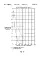
- FIGS. 1 and 2are absorption curves for silicon.
- FIG. 3is a drawing of a laser beam focused onto a small spot on a focal plane.
- FIG. 4is a plot of the power density of a laser beam spot on a work piece as a function of the spot's distance from the focus of the laser beam.
- FIG. 5is a block diagram of a memory repair system that operates at 1.198 ⁇ m.
- FIG. 6is a perspective diagrammatic view of a link of a memory on its substrate.
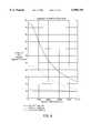
- FIG. 7is a plot of temperature at the interface between the silicon dioxide layer and the silicon substrate in FIG. 6, as a function of the thickness of the silicon dioxide layer.
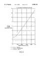
- FIG. 8is a plot of energy per pulse for a neodymium vanadate laser over a range of repetition rates of the pulses.
- FIG. 9is a plot of pulse width for a neodymium vanadate laser over a range of repetition rates of the pulses.
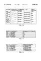
- FIG. 10is a table of stimulated cross section, fluorescent lifetime, I sat , and single-pass gain for various laser materials at various wavelengths.
- FIG. 11is a table of optimum output couplers for various laser materials at various wavelengths.
- FIG. 12is a table of minimum pulse widths for various laser materials at various wavelengths.
- FIGS. 13-15are plots of pulse widths of different materials at shorter wavelengths (1.047 microns and 1.064 microns) and longer wavelengths (1.32 microns and 1.34 microns).
- FIG. 16is a block diagram similar to FIG. 5, operating at 1.064 ⁇ m.
- FIG. 17is a side view of the system of FIG. 16 showing the replaceable addition of a wavelength shifter to achieve the system of FIG. 5.
- FIG. 18is a drawing of a neodynium vanadate laser and a barium nitrate Raman wavelength shifter.
- the techniques of the present inventionprovide quick and reliable removal of links in semiconductor memory devices. By increasing the probability of success of removing individual links, the invention increases the overall probability of successfully repairing a given semiconductor device having many links to be removed, thereby providing successful yields of repaired semiconductor devices.
- the increased probability of success of removing individual linksis particularly valuable because the probability of successfully repairing a semiconductor device varies exponentially with the probability of successfully removing individual links.
- the probability P of repairing a semiconductor deviceis:
- the probability P of repairing the entire semiconductor deviceis 98.8 percent.
- the probability Pdrops to 61 percent.
- the techniques of the present inventionalso provide a high-gain laser system at high manufacturing throughput. This is especially important because the pulse-to-pulse power stability of laser pulses at high repetition rates (high throughput) can be adversely affected if the gain of the laser system is too low.
- the inventionreduces this variation in output and thereby improves the ability of the laser system to successfully remove links at high throughput, which is particularly valuable due to the increasing absolute number of links per semiconductor device (the speed of link removal has increased from 100 links per second up to 10,000 links per second for recent devices).
- the gain of the laser systemis improved as compared with operation at 1.32 ⁇ m (as is explained in detail below), thereby improving pulse-to-pulse stability and the overall probability of successfully removing each link.
- the improved gain provided by the techniques of the present inventionis also important because short laser pulses, which prevent heat from dissipating into the silicon substrate and adjacent structures of a memory device, require a high gain.
- FIGS. 1 and 2are curves that show the absorption of silicon as a function of wavelength at approximately room temperature.
- the absorptionrapidly drops off after about one micron.
- the absorption edgeis typically about 1.12 microns.
- the siliconstarts to transmit more and more easily, and thus it is possible to obtain better part yields upon removing material from the silicon substrate.
- Absorption in siliconcan be divided into three areas of interest. The first is for wavelengths shorter than those corresponding to the absorption edge ("below the absorption edge"), the second is the transition region near the absorption edge, and the third is for longer wavelengths ("beyond the absorption edge"). For wavelengths below the absorption edge the strong absorption is due to carriers being raised from the valence band to the conduction band. In the long wavelength region the absorption is due to free carriers, crystal lattice vibrations, absorption in impurities, etc., and in this range the absorption is minimal. For the wavelength under consideration, the transition region is of prime interest.
- FIGS. 1 and 2provide detail of the absorption in this transition region.
- the absorption coefficientdecrease by a factor of four orders of magnitude going from 0.9 microns to 1.2 microns.
- the curveshows a drop of two orders of magnitude.
- xis the thickness of the sample (1 millimeter)
- Iis the energy level at the distance x into the substrate
- I 0is the incident energy at the surface of the silicon
- ⁇is the absorption coefficient.
- the absorption coefficient ⁇is 20 cm -1 for 1.047 microns and 0.1 cm -1 for 1.2 microns.
- 86.5 percent of the energyis absorbed in the silicon substrate at 1.047 microns wavelength and 1 percent of the energy is absorbed at 1.2 microns. This shows a drastic change in absorption for a very slight change in wavelength.
- operating the laser at a wavelength beyond the absorption edge of the substratecircumvents damage to the substrate, which is especially important if there is a slight mis-alignment of the laser beam with respect to the link.
- the laser beam outputis beyond the absorption edge of silicon but is constrained to less than 1.2 microns, rather than a wavelength that optimizes the transmissivity of silicon.
- the laser beam output, constrained to less than 1.2 microns,produces a sharply defined spot and good depth of focus for reasons explained below.
- the ability of a lens 36 to focus to a small spot 38is dependent upon the wavelength of the laser, the size of the laser beam as it enters the lens, and the focal length of the lens.
- the spot size at the focus of a lens subsystemis given by: ##EQU1## where ⁇ is the laser wavelength and K is a constant dependent upon lens design (typically between 1.83 and 2).
- F# of the lensthe focal length divided by the input beam diameter
- the lens approaches an F# of oneextreme care must be taken in lens design.
- the focused spot sizeis 2.6 microns. This is very much in the realm of the focused spot size required of memory repair.
- Klens constant
- increasing the wavelength from 1.047 microns to 1.198 micronsincreases the spot size by 14 percent.
- Increasing the wavelength from 1.047 microns to 1.318 micronsincreases the spot size by 26 percent. Therefore, it is advantageous to keep the wavelength as short as possible and still have the benefit of the decreased absorption by operating the laser at a wavelength beyond the absorption edge of the substrate.
- depth of focusis defined as the distance over which spot diameter remains reasonably constant.
- the depth of focusvaries inversely to the square of the spot size and inversely to the wavelength of the laser.
- the depth of focus at 1.047 micronsis plus or minus five microns.
- AT 1.32 micronsthe depth of focus drops to plus or minus four microns. This is a substantial difference.
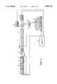
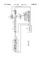
- Laser 10is constructed to operate at wavelength ⁇ 1 , 1.064 ⁇ m, which is less than the absorption edge of silicon. It is aligned to a wavelength shifter 12 that is constructed to shift to a wavelength beyond the absorption edge of silicon.
- the beamis then passed through a controlled electro-acousto-optic attenuator 13, expanded by a telescope 14, and, at a scanning head 15, is scanned over a focusing lens 16 by two scanner galvanometers, 18 and 20. The spot is focused onto wafer 22 for removing links 24, under control of computer 33.
- the laser 10is mounted on a stable platform 11 relative to the galvanometers and the work piece. It is controlled from outside of the laser itself by computer 33 to transmit its beam to the scanner head comprising the accurate X and Y galvanometers 18 and 20. It is very important, in removing links that the beam be positioned with accuracy of less than 3/10 of a micron. The timing of the laser pulse to correlate with the position of the continually moving galvanometers is important.
- the system computer 33asks for a laser pulse on demand.
- a step and repeat table 34moves the wafer into position to treat each memory die.
- the laser 10is a neodymium vanadate laser, with an overall length L of about 6 inches, and a short cavity length.
- the shifter 12 of this preferred embodimentis external to the cavity, and is about another 4 inches long.
- the laseris a Q-switched diode pumped laser, of sufficient length and construction to enable external control of pulse rate with high accuracy by computer 33.
- the cavity of the laserincludes a partially transmissive mirror 7, optimized at ⁇ 1 , which is the wavelength at which the lasing rod 6 of neodymium vanadate is pumped by the diode.
- the partially transmissive output mirror 9is also optimized at ⁇ 1 .
- the pumping diode 4produces between about one and two watts depending on the design. It focuses onto the rear of the laser rod 6.
- the laser rodis coated, on its pumped end, with a mirror 7 appropriate for the standard laser wavelength of 1.064 nm.
- the other end of the rodis coated with a dichroic coating.
- an optical Q-switch 8in the form of an acousto-optic modulator. It is used as the shutter for establishing the operating frequency of the laser.
- the output mirror 9The two mirrors, 7 on the pumped end of the laser rod and 9 beyond the acoustic optical Q-switch, comprise the laser cavity.
- a system optical switch 13 in the form of a further acousto-optic attenuatoris positioned beyond the laser cavity, in the laser output beam. Under control of computer 33, it serves both to prevent the beam from reaching the galvanometers except when desired, and, when the beam is desired at the galvanometers, to controllably reduce the power of the laser beam to the desired power level.
- this power levelmay be as little as 10 percent of the gross laser output, depending upon operating parameters of the system and process.
- the power levelmay be about 0.1 percent of the gross laser output during alignment procedures in which the laser output beam is aligned with the target structure prior to a vaporization procedure.
- the positions of the X, Y galvanometers 10 and 12are controlled by the computer 33 by galvanometer control G.
- the galvanometersmove at constant speed over the memory device on the silicon wafer.
- the laseris controlled by timing signals based on the timing signals that control the galvanometers.
- the laseroperates at a constant repetition rate and is synchronized to the galvanometers by the system optical switch 13.
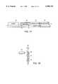
- the laser beamis shown focused upon the wafer.
- the laser beamis seen being focused on a link element 25 of a memory circuit.
- the spot sizeis typically 3 to 4 microns in diameter, with peak power occurring in the center of the spot in accordance with a gaussian distribution, and with lower power occurring at the edges.
- the link 25is somewhat smaller than the spot size.
- a linkmay be for instance 1 micron wide and about 1/3 micron thick. In the case demonstrated here the link is made of metal.
- the metal linkis supported on the silicon substrate 30 by silicon dioxide insulator layer 32, which may be, e.g., 0.3-0.5 microns thick. Over the link is another layer of silicon dioxide (not shown).
- silicon dioxideover the link is another layer of silicon dioxide (not shown).
- the laser beamimpinges on the link and heats it to the melting point. During the heating the metal is prevented from vaporizing by the confining effect of the overlying layer of oxide. During the duration of the short pulse, the laser beam progressively heats the metal, until the metal so expands that the insulator material ruptures. At this point, the molten material is under such high pressure that it instantly vaporizes and blows cleanly out through the rupture hole.
- silicon dioxide layer 32 between silicon substrate 30 and link 25is about 3000 to 5000 Angstroms (0.3 microns to 0.5 microns) thick. This structure is shown in FIG. 6.
- the heatis conducted to substrate 30 and along link 25 as shown.
- the amount of heat that is transferred to substrate 30 through silicon dioxide layer 32is dependent upon the material characteristics of the oxide (the thermal diffusivity), the thickness of oxide layer 32, and the length of the laser pulse. The calculation of this thermal transfer is quite complex, but a qualitative feel for the effect can be indicated by the formula for temperature T at the interface between oxide layer 32 and silicon substrate 30:
- short laser pulsesare advantageous in processing high-density memories because the short pulse contains the heating of material to the link area. Short pulses prevent the heat from dissipating into the silicon substrate and adjacent structures, thus causing collateral damage. Hence, it is desirable to use conventional lasers with short laser pulse capabilities.
- the silicon substrateis kept relatively cool both by appropriate selection of wavelength and by limiting the pulse duration, with a correspondingly high peak pulse.
- the silicondoes not have the capability to absorb very much of the energy, while most of the heat is confined to the link by keeping the pulse short.
- FIGS. 8 and 9we show a plot of the energy as a function of repetition rate, and also the minimum obtainable pulse width as a function of repetition rate, for the neodymium vanadate laser.
- the pulse widthis short up to about 10 Khz and the energy stays nearly constant up to that level. In most circumstances, it is highly advantageous to operate the laser in the higher repetition rate range to achieve high productivity and speedy handling of the wafer.
- a 256 megabit memory deviceis typically about 10 mm wide and as much as 1.8 cm long.
- a 256 megabit memory devicestores 256 million bits of information.
- the memoriesare tested before memory repair is conducted.
- memories like thisthere are rows or columns of elements, with a number of redundant rows. If a bad row is found, it is recorded and is subsequently surgically removed in the manner that has been described, and a spare row is programmed in to the circuit by also removing links to switch transistors.
- a conventional laser 10 with a very short pulse widthdesigned to maintain this pulse width over a substantial range of laser repetition rates, is introduced into a system that includes a wavelength shifter 12.
- the conventional laser 10 at 1.064 microns or 1.047 micronstypically has a very high gain and can be easily designed to develop the requisite short pulse.
- a laser configured to intrinsically have the longer wavelengthsuch as the 1.32-micron wavelength of YAG or YLF, would have intrinsically low gain and hence will have a pulse width much longer than desired.
- the Nd:YVO 4 (vanadate) laser 10has very high gain and constant pulse width at high repetition rates operating at 1.064 microns.
- the wavelength shifter 12(such as a stimulated Raman scattering laser) can shift the wavelength to beyond the absorption edge of silicon without increasing the laser pulse width.
- the energy per pulse required to remove linksis extremely small and can be easily provided by any of the laser types to be discussed. What is important in memory repair in accordance with the present invention is a short laser pulse.
- a laser operated at a standard wavelengthcan produce pulses shorter than can be produced by the same laser operated at a longer wavelength.
- the single pass gain of the laseris an important performance parameter of a laser.
- the optical power gainmust be greater than the losses within the cavity.
- the laser thresholdis defined as the point at which the optical gain is equal to the losses.
- the pulse widthis dependent upon the length of the cavity, the transmission of the output coupler (the front mirror), and the magnitude of the gain over its threshold level.
- Eis the efficiency of conversion of pump light to laser output
- Pis the pump power (i.e., the effective power delivered by the laser diode)
- I satis a material parameter dependent on the laser material and its doping
- a pumpis the cross-sectional area covered by the pump beam in the laser rod
- a modeis the cross-sectional area of the laser mode within the laser rod.
- the gainis dependent on laser system design.
- the pump efficiency Eis about 25 percent
- the effective pump power used Pis 0.7 watts
- the pump area A pumpis 0.46 square millimeters
- the laser mode cross-sectional area A modeis 0.015 square millimeters.
- I satthe material-dependent parameter, relates to the storage time capabilities of the laser material and its "lasing cross section for stimulated emission.” The higher the cross section, the higher the gain.
- This material-dependent parameteris given by:
- hPlanck's constant
- vthe frequency of light (the speed of light c divided by the lasing wavelength ⁇ )
- ⁇the cross section for stimulated emission
- ⁇the energy storage time or "the upper state lifetime.”
- ⁇ , ⁇ , I sat , and single-pass gain for the typical laser materialsare given in the table of FIG. 10. This table shows that at the 1.32-micron wavelength for YAG and YLF lasers the single-pass gain is much less than at 1.064 and 1.047 microns. Preferably, the single-pass gain should be about 20 percent or greater, and the fluorescent lifetime should be less than about 100 microseconds
- the single-pass lossis approximately 0.66 percent.
- the gainis dependent on the laser material.
- the output couplers for various materialsare shown in the table of FIG. 11. Preferably the optimum output coupler should be greater than 5 percent.
- the duration of the Q-switched pulse(laser pulse width) can be calculated.
- the Q-switched pulse widthis a multiple of the cavity decay time t c , which is defined as the time taken for 63 percent of the light in the laser resonator to exit from the mirror of the laser. This time is given by:
- Lis the cavity length (20 mm for the Light Wave Model 110 laser)
- Tis the transmission of the output coupler
- cis the speed of light
- nis the average index of refraction of the laser cavity (assumed to be 1.48). Knowing the ratio of stored energy versus threshold energy, one can calculate the laser pulse width as follows:
- ⁇ pis the laser pulse width
- ris the initial ratio of the energy stored in the cavity versus the threshold energy (this is the round trip gain (2 ⁇ single-pass gain)/mirror transmission)
- n (r)is the efficiency of the Q switch in extracting the stored energy ( n (r) is 1 for r ⁇ 2).
- the pulse widths for various materials and wavelengthsare shown in the table of FIG. 12.
- the maximum energy that can be delivered by a laseris a function of the maximum laser power and the storage time (the "upper state lifetime"), and is given by:
- E maxis the maximum energy that can be extracted from the laser
- P cwis the maximum average power of the laser
- ⁇is the storage time or "upper state lifetime.”
- tis the time between laser pulses (the inverse of the repetition rate).
- the pulse widthbe substantially flat with respect to repetition rate, i.e., that it should vary no more than about 25 percent from zero to 10 kilohertz.
- the longer storage time of the YLF laseryields much higher energy per pulse but has the most change in energy as a function of repetition rate.
- the vanadate laserhas the lowest energy per pulse but has relatively less drop off as a function of repetition rate.
- the vanadate characteristics of energy versus repetition rateare much more desirable. Since the upper state storage time for 1.32 microns is similar to the 1.047 and 1.064 micron levels, the energy versus repetition rate is about the same.
- FIG. 9shows the pulse width for the three different materials as a function of repetition rate. Not only does the YVO 4 (vanadate) have the shortest pulse width, but it maintains this pulse width over a very wide range.
- FIGS. 13, 14, and 15compare the pulse widths of different materials at the shorter wavelengths (1.047 microns and 1.064 microns) with the longer wavelengths at 1.32 microns and 1.34 microns. In these graphs the pulse width is very much affected by going to the longer wavelengths.
- SRS laser 12is predicted to have a 50 percent efficiency in energy conversion, and the laser pulse width produced by SRS laser 12 will be the same as or a little shorter than the laser pulse width produced by conventional laser 10.
- SRS laser 12has the additional advantage of shifting to a wavelength somewhat shorter than the 1.32 micron and 1.34 micron wavelengths produced by YAG, YLF, or YVO 4 lasers.
- the vanadate laser(YVO 4 ) has the best performance as conventional laser 10 because it provides the shortest laser pulse and maintains this short pulse over the required pulse repetition rate.
- the stimulated raman scattering laser 12shifts the 1.064-micron wavelength to beyond the absorption edge of silicon, and so improves the memory repair process.
- FIG. 5shows wavelength shifter 12 in place.
- the shifteris constructed to be removable and the system made operable without it in place.
- Semiconductor memory facilitiesusually employ a number or processes that have been established over a period of time. For example a 1 megabit memory may be produced one day, which has polysilicon links, which are removed efficiently using the standard wavelength of 1.064 ⁇ m. The next day a newer device may be produced which has metal links and are advantageously removed by the system just described.
- the shifteris constructed to be moved in and out of the beam line.
- the shifteris pre-aligned and accurately point pinned by pins 31 into the stable structural base plate 11 of the laser system (see FIG. 17).
- everything elsei.e., the laser, the system switch 13, etc.
- FIG. 16shows the system of FIG. 5 with the shifter removed for removing links using a treatment beam of 1.064 ⁇ m. To operate at the longer wavelength, the shifter is replaced in its pins and no realignment is required.
- the inventioncan be implemented using neodymium vanadate lasers and using a removable solid-state, stimulated Raman scatter shifter.
- Barium nitrate Raman shiftersappear to be especially useful because they have a high damage threshold (they are not easily damaged by high-density laser beams).
- FIG. 18One particular implementation of a barium nitrate Raman shifter is shown in FIG. 18.
- Vanadate laser 10produces a light beam that impinges on dichroic mirror 40, which is highly reflective at 1.064 microns but highly transmissive at 1.198 microns.
- the 1.064-micron wavelength light from laser 10is reflected into barium nitrate wavelength shifter 12, which shifts wavelength of the light to 1.198 microns.
- the 1.198-micron wavelength lightis reflected between mirror 42, which is highly reflective at 1.198 microns, and mirror 44, which is 50-percent reflective at 1.198 microns (in order to let some of the 1.198-micron wavelength light escape as the output of wavelength shifter 12).
- Mirrors 44 and 40are both highly reflective at 1.064 microns, and so any 1.064-micron light is reflected back into vanadate laser 10.
- Raman shifter 12could be incorporated into laser 10 (i.e., laser 10 could be a Raman-shifted laser).
- tunable lasersare operable.
- Fosterite lasershave a tunable region that essentially straddles the absorption edge region of silicon, and can permit operation both beyond and below the absorption edge of silicon. At the present state of the art, they do not appear to be as efficient as they may become in time. As materials and improvements are being continually developed in the laser field, it is within the invention to use such devices and obtain benefits according to certain of the broad aspects of the present invention.
- Short pulse laser operationis desirable for thin metal and polysilicon links because short pulses limit the time of heat dissipation to surrounding structures, especially the silicon substrate.
- the best fit to the above criteriaappears to be to operate a high-gain laser (vanadate, for example) at a conventional wavelength. These lasers run below the absorption edge of the silicon substrate. It is desirable to shift the wavelength to beyond the absorption edge with a wavelength shifter such as a stimulated Raman scattering laser. This technique produces the best solution for memory repair--a short-pulse, long-wavelength laser system.
Landscapes
- Physics & Mathematics (AREA)
- Engineering & Computer Science (AREA)
- Optics & Photonics (AREA)
- Plasma & Fusion (AREA)
- Mechanical Engineering (AREA)
- Condensed Matter Physics & Semiconductors (AREA)
- General Physics & Mathematics (AREA)
- Manufacturing & Machinery (AREA)
- Computer Hardware Design (AREA)
- Microelectronics & Electronic Packaging (AREA)
- Power Engineering (AREA)
- Laser Beam Processing (AREA)
- Lasers (AREA)
Abstract
Description
P=p.sup.n.
Absorption=1-I/I.sub.0 =1-exp(-αx)
Depth of Focus=(Spot Size).sup.2 /[3×(Laser Wavelength)].
T(z,t)=Ts{1-erf[z/2(κt).sup.1/2 ]}, where ##EQU2## Ts is the surface temperature, z is the thickness of the layer (for oxide this is 0.3 microns), κ is the thermal diffusivity of the silicon dioxide layer, and t is the length of the laser pulse. T(z,t)/Ts is plotted in FIG. 7 for the silicon dioxide layer for two laser pulse widths of 3 nanoseconds and 20 nanoseconds. The curves in FIG. 7 clearly show that using a shorter pulse width helps in preventing heat from being conducted into the silicon substrate.Gain=EP/[I.sub.sat (A.sub.pump +A.sub.mode)
I.sub.sat =hv/στ
T.sub.optimum =2[(gain×loss).sup.1/2 -loss].
t.sub.c =2Ln/cT
τ.sub.p ={r.sup.n (r)/[r-1-ln(r)]}×τ.sub.cE.sub.max =P.sub.cw τ
E=E.sub.max [1-exp(-t/τ)];
T.sub.p -τ.sub.p /[1-exp(-t/τ)],
Claims (45)
Priority Applications (7)
| Application Number | Priority Date | Filing Date | Title |
|---|---|---|---|
| US08/774,107US5998759A (en) | 1996-12-24 | 1996-12-24 | Laser processing |
| PCT/US1997/023132WO1998028104A1 (en) | 1996-12-24 | 1997-12-10 | Shifted wavelength laser processing of circuit links |
| TW086119123ATW356613B (en) | 1996-12-24 | 1997-12-17 | Laser work |
| US09/441,201US6337462B1 (en) | 1996-12-24 | 1999-11-16 | Laser processing |
| US10/036,431US6791059B2 (en) | 1996-12-24 | 2002-01-07 | Laser processing |
| US10/899,133US6878899B2 (en) | 1996-12-24 | 2004-07-27 | Laser processing |
| US11/099,584US20050173385A1 (en) | 1996-12-24 | 2005-04-06 | Laser processing |
Applications Claiming Priority (1)
| Application Number | Priority Date | Filing Date | Title |
|---|---|---|---|
| US08/774,107US5998759A (en) | 1996-12-24 | 1996-12-24 | Laser processing |
Related Child Applications (1)
| Application Number | Title | Priority Date | Filing Date |
|---|---|---|---|
| US09/441,201ContinuationUS6337462B1 (en) | 1996-12-24 | 1999-11-16 | Laser processing |
Publications (1)
| Publication Number | Publication Date |
|---|---|
| US5998759Atrue US5998759A (en) | 1999-12-07 |
Family
ID=25100264
Family Applications (5)
| Application Number | Title | Priority Date | Filing Date |
|---|---|---|---|
| US08/774,107Expired - LifetimeUS5998759A (en) | 1996-12-24 | 1996-12-24 | Laser processing |
| US09/441,201Expired - LifetimeUS6337462B1 (en) | 1996-12-24 | 1999-11-16 | Laser processing |
| US10/036,431Expired - LifetimeUS6791059B2 (en) | 1996-12-24 | 2002-01-07 | Laser processing |
| US10/899,133Expired - LifetimeUS6878899B2 (en) | 1996-12-24 | 2004-07-27 | Laser processing |
| US11/099,584AbandonedUS20050173385A1 (en) | 1996-12-24 | 2005-04-06 | Laser processing |
Family Applications After (4)
| Application Number | Title | Priority Date | Filing Date |
|---|---|---|---|
| US09/441,201Expired - LifetimeUS6337462B1 (en) | 1996-12-24 | 1999-11-16 | Laser processing |
| US10/036,431Expired - LifetimeUS6791059B2 (en) | 1996-12-24 | 2002-01-07 | Laser processing |
| US10/899,133Expired - LifetimeUS6878899B2 (en) | 1996-12-24 | 2004-07-27 | Laser processing |
| US11/099,584AbandonedUS20050173385A1 (en) | 1996-12-24 | 2005-04-06 | Laser processing |
Country Status (3)
| Country | Link |
|---|---|
| US (5) | US5998759A (en) |
| TW (1) | TW356613B (en) |
| WO (1) | WO1998028104A1 (en) |
Cited By (72)
| Publication number | Priority date | Publication date | Assignee | Title |
|---|---|---|---|---|
| US6114652A (en)* | 1998-09-10 | 2000-09-05 | Northrop Grumman Corporation | Method of forming acoustic attenuation chambers using laser processing of multi-layered polymer films |
| US6186384B1 (en)* | 1998-02-27 | 2001-02-13 | Nec Corporation | Method of cleaving a brittle material using a point heat source for providing a thermal stress |
| WO2001047659A1 (en)* | 1999-12-28 | 2001-07-05 | Gsi Lumonics, Inc. | Energy-efficient, laser-based method and system for processing target material |
| WO2002030610A1 (en)* | 2000-10-09 | 2002-04-18 | Optische Werke G. Rodenstock | Method for characterizing and especially for labeling the surfaces of optical elements by means of uv light |
| US20020048864A1 (en)* | 1999-08-13 | 2002-04-25 | Shunpei Yamazaki | Laser apparatus, laser annealing method, and manufacturing method of a semiconductor device |
| WO2001098016A3 (en)* | 2000-06-01 | 2002-06-27 | Gen Scanning Inc | Laser system for processing target material |
| US20020093997A1 (en)* | 1996-12-24 | 2002-07-18 | General Scanning, A Massachusetts Corporation | Laser processing |
| WO2001087534A3 (en)* | 2000-05-16 | 2002-07-25 | Gen Scanning Inc | Method and system for precisely positioning a waist of a material-processing laser beam to process microstructures within a laser-processing site |
| US6461929B1 (en)* | 1999-01-16 | 2002-10-08 | Koninklijke Philips Electronics N.V. | Method for the fine tuning of a passive electronic component |
| US20020162973A1 (en)* | 2001-03-29 | 2002-11-07 | Cordingley James J. | Methods and systems for processing a device, methods and systems for modeling same and the device |
| US6501045B1 (en)* | 2000-04-06 | 2002-12-31 | Resonetics, Inc. | Method and apparatus for controlling the taper angle of the walls of laser machined features |
| US6526089B1 (en) | 1999-09-29 | 2003-02-25 | Sunx Limited | Laser marker and method of light spot adjustment therefor |
| EP1291118A1 (en)* | 2001-09-07 | 2003-03-12 | TRUMPF LASERTECHNIK GmbH | Process and device for deepening holes in a multilayer circuit board |
| US20030047541A1 (en)* | 2001-03-12 | 2003-03-13 | Yunlong Sun | Quasi-CW diode-pumped, solid-state harmonic laser system and method employing same |
| US6574250B2 (en) | 2000-01-10 | 2003-06-03 | Electro Scientific Industries, Inc. | Laser system and method for processing a memory link with a burst of laser pulses having ultrashort pulse widths |
| US20030164873A1 (en)* | 2001-11-07 | 2003-09-04 | Fuji Photo Film Co., Ltd. | Photosensitive material and laser marking method |
| US20030189032A1 (en)* | 1998-12-16 | 2003-10-09 | General Scanning, A Massachusetts Corporation | Laser processing |
| US20040031779A1 (en)* | 2002-05-17 | 2004-02-19 | Cahill Steven P. | Method and system for calibrating a laser processing system and laser marking system utilizing same |
| US6723977B1 (en)* | 2000-01-06 | 2004-04-20 | Raytheon Company | System and method for sensing atmospheric contaminants using transmitter with dual optical parametric oscillators and receiver for the same |
| US20040100999A1 (en)* | 2002-11-21 | 2004-05-27 | New Wave Research | Dual head laser system with intra-cavity polarization, and particle image velocimetry system using same |
| US6744228B1 (en) | 1998-09-18 | 2004-06-01 | Gsi Lumonics Corp. | High-speed precision positioning apparatus |
| US20040104202A1 (en)* | 2000-01-28 | 2004-06-03 | Gsi Lumonics, Inc. | Laser scanning method and system for marking articles such as printed circuit boards, integrated circuits and the like |
| US20040112879A1 (en)* | 2002-12-16 | 2004-06-17 | Masaki Mori | Identification-code laser marking method and apparatus |
| US20040200818A1 (en)* | 2001-12-18 | 2004-10-14 | Yasufumi Yamada | Method and apparatus for processing three-dimensional structure, method for producing three-dimensional shape product and three-dimensional structure |
| US6806440B2 (en) | 2001-03-12 | 2004-10-19 | Electro Scientific Industries, Inc. | Quasi-CW diode pumped, solid-state UV laser system and method employing same |
| US20040226925A1 (en)* | 2003-03-07 | 2004-11-18 | Bo Gu | Laser system and method for material processing with ultra fast lasers |
| US6841482B2 (en)* | 2000-12-15 | 2005-01-11 | Xsil Technology Limited | Laser machining of semiconductor materials |
| US20050067388A1 (en)* | 2003-08-19 | 2005-03-31 | Yunlong Sun | Methods of and laser systems for link processing using laser pulses with specially tailored power profiles |
| US6885683B1 (en)* | 2000-05-23 | 2005-04-26 | Imra America, Inc. | Modular, high energy, widely-tunable ultrafast fiber source |
| US6887804B2 (en) | 2000-01-10 | 2005-05-03 | Electro Scientific Industries, Inc. | Passivation processing over a memory link |
| US20050161444A1 (en)* | 2003-10-17 | 2005-07-28 | Gsi Lumonics Corporation | Flexible scan field |
| US20050205537A1 (en)* | 2004-03-18 | 2005-09-22 | Trotec Produktions U. Vertriebs Gmbh | Processing device and method of controlling same |
| US20050224469A1 (en)* | 2003-06-30 | 2005-10-13 | Cutler Donald R | Efficient micro-machining apparatus and method employing multiple laser beams |
| US20050277028A1 (en)* | 2001-10-30 | 2005-12-15 | Semiconductor Energy Laboratory Co., Ltd. | Laser apparatus, laser irradiation method, manufacturing method for semiconductor device, semiconductor device, production system for semiconductor device using the laser apparatus, and electronic equipment |
| US20050282367A1 (en)* | 2004-06-18 | 2005-12-22 | Bruland Kelly J | Semiconductor structure processing using multiple laser beam spots spaced on-axis on non-adjacent structures |
| US20050281101A1 (en)* | 2004-06-18 | 2005-12-22 | Bruland Kelly J | Semiconductor structure processing using multiple laterally spaced laser beam spots with on-axis offset |
| US20050281102A1 (en)* | 2004-06-18 | 2005-12-22 | Bruland Kelly J | Semiconductor structure processing using multiple laterally spaced laser beam spots with joint velocity profiling |
| US20050282406A1 (en)* | 2004-06-18 | 2005-12-22 | Bruland Kelly J | Semiconductor structure processing using multiple laterally spaced laser beam spots delivering multiple blows |
| US20050282407A1 (en)* | 2004-06-18 | 2005-12-22 | Bruland Kelly J | Semiconductor structure processing using multiple laser beam spots spaced on-axis delivered simultaneously |
| US20050279736A1 (en)* | 2004-06-18 | 2005-12-22 | Bruland Kelly J | Semiconductor structure processing using multiple laser beam spots spaced on-axis with cross-axis offset |
| US20050282319A1 (en)* | 2004-06-18 | 2005-12-22 | Bruland Kelly J | Semiconductor structure processing using multiple laser beam spots overlapping lengthwise on a structure |
| US20060000813A1 (en)* | 2004-05-18 | 2006-01-05 | Airbus Deutschland Gmbh | Laser-assisted coating removal method |
| US6987786B2 (en) | 1998-07-02 | 2006-01-17 | Gsi Group Corporation | Controlling laser polarization |
| US20060018350A1 (en)* | 2004-07-20 | 2006-01-26 | Lightwave Electronics Corporation | Laser burst boosting method and apparatus |
| US20060114948A1 (en)* | 2004-11-29 | 2006-06-01 | Lo Ho W | Workpiece processing system using a common imaged optical assembly to shape the spatial distributions of light energy of multiple laser beams |
| US20060128073A1 (en)* | 2004-12-09 | 2006-06-15 | Yunlong Sun | Multiple-wavelength laser micromachining of semiconductor devices |
| US20060124611A1 (en)* | 2004-12-14 | 2006-06-15 | Chih-Ming Hsu | High-power-laser chip-fabrication apparatus and method thereof |
| US20060289411A1 (en)* | 2005-06-24 | 2006-12-28 | New Wave Research | Laser system with multiple operating modes and work station using same |
| US20070000428A1 (en)* | 2001-11-27 | 2007-01-04 | Semiconductor Energy Laboratory Co., Ltd. | Laser irradiation apparatus |
| US20070173075A1 (en)* | 2001-03-29 | 2007-07-26 | Joohan Lee | Laser-based method and system for processing a multi-material device having conductive link structures |
| US7289549B2 (en) | 2004-12-09 | 2007-10-30 | Electro Scientific Industries, Inc. | Lasers for synchronized pulse shape tailoring |
| US20080029491A1 (en)* | 2006-07-20 | 2008-02-07 | Gsi Group Corporation | System and method for laser processing at non-constant velocities |
| US20080067155A1 (en)* | 2006-09-15 | 2008-03-20 | Bo Gu | Method and system for laser processing targets of different types on a workpiece |
| US20080121627A1 (en)* | 2004-06-18 | 2008-05-29 | Electro Scientific Industries, Inc. | Methods and systems for semiconductor structure processing using multiple laser beam spots |
| US20080164240A1 (en)* | 2007-01-05 | 2008-07-10 | Gsi Group Corporation | System and method for multi-pulse laser processing |
| US7469831B2 (en) | 2004-06-30 | 2008-12-30 | Gsi Group Corporation | Laser-based method and system for processing targeted surface material and article produced thereby |
| US20090095722A1 (en)* | 2007-09-19 | 2009-04-16 | Gsi Group Corporation | Link processing with high speed beam deflection |
| US20090245301A1 (en)* | 2008-03-27 | 2009-10-01 | Electro Sciencitfic Industries, Inc. | Laser micromachining using programmable pulse shapes |
| US7671295B2 (en) | 2000-01-10 | 2010-03-02 | Electro Scientific Industries, Inc. | Processing a memory link with a set of at least two laser pulses |
| US7723642B2 (en) | 1999-12-28 | 2010-05-25 | Gsi Group Corporation | Laser-based system for memory link processing with picosecond lasers |
| US7838794B2 (en) | 1999-12-28 | 2010-11-23 | Gsi Group Corporation | Laser-based method and system for removing one or more target link structures |
| US7871903B2 (en) | 2002-03-27 | 2011-01-18 | Gsi Group Corporation | Method and system for high-speed, precise micromachining an array of devices |
| US20110210105A1 (en)* | 2009-12-30 | 2011-09-01 | Gsi Group Corporation | Link processing with high speed beam deflection |
| USRE43487E1 (en) | 2000-09-20 | 2012-06-26 | Electro Scientific Industries, Inc. | Laser segmented cutting |
| US20130068736A1 (en)* | 2011-09-21 | 2013-03-21 | Michael Mielke | Systems and processes that singulate materials |
| US20140014631A1 (en)* | 2012-07-10 | 2014-01-16 | Disco Corporation | Laser processing method |
| US20150209902A1 (en)* | 2010-10-21 | 2015-07-30 | Electro Scientific Industries, Inc. | Method and apparatus for optimally laser marking articles |
| US9209592B2 (en) | 2004-03-25 | 2015-12-08 | Imra America, Inc. | Optical parametric amplification, optical parametric generation, and optical pumping in optical fibers systems |
| US9815141B2 (en) | 2011-12-07 | 2017-11-14 | General Atomics | Methods and systems for use in laser machining |
| DE102019135850A1 (en) | 2019-01-02 | 2020-07-02 | Faurecia Sièges d'Automobile | Actuator for a vehicle seat and vehicle seat |
| US10906073B2 (en)* | 2017-09-05 | 2021-02-02 | Chengdu Mrj-Laser Technology Co., Ltd. | Adjustable focus laser cleaning galvanometer, cleaning system and cleaning method |
| US11413704B2 (en)* | 2019-07-17 | 2022-08-16 | Fanuc Corporation | Adjustment assistance device and laser welding apparatus |
Families Citing this family (60)
| Publication number | Priority date | Publication date | Assignee | Title |
|---|---|---|---|---|
| US20050281887A1 (en)* | 1995-08-31 | 2005-12-22 | Rizoiu Ioana M | Fluid conditioning system |
| US20060241574A1 (en)* | 1995-08-31 | 2006-10-26 | Rizoiu Ioana M | Electromagnetic energy distributions for electromagnetically induced disruptive cutting |
| US20060240381A1 (en) | 1995-08-31 | 2006-10-26 | Biolase Technology, Inc. | Fluid conditioning system |
| US6288499B1 (en)* | 1997-06-12 | 2001-09-11 | Biolase Technology, Inc. | Electromagnetic energy distributions for electromagnetically induced mechanical cutting |
| US20030222324A1 (en)* | 2000-01-10 | 2003-12-04 | Yunlong Sun | Laser systems for passivation or link processing with a set of laser pulses |
| US20060141681A1 (en)* | 2000-01-10 | 2006-06-29 | Yunlong Sun | Processing a memory link with a set of at least two laser pulses |
| US20080157690A1 (en)* | 2001-05-02 | 2008-07-03 | Biolase Technology, Inc. | Electromagnetic energy distributions for electromagnetically induced mechanical cutting |
| KR100614106B1 (en)* | 2002-03-12 | 2006-08-22 | 미쓰보시 다이야몬도 고교 가부시키가이샤 | Processing method and apparatus for brittle materials |
| TWI326626B (en) | 2002-03-12 | 2010-07-01 | Hamamatsu Photonics Kk | Laser processing method |
| EP1494572A4 (en)* | 2002-03-27 | 2010-11-10 | Hadasit Med Res Service | Controlled laser treatment for non-invasive tissue alteration, treatment and diagnostics with minimal collateral damage |
| US7259906B1 (en) | 2002-09-03 | 2007-08-21 | Cheetah Omni, Llc | System and method for voice control of medical devices |
| JP4531323B2 (en)* | 2002-09-13 | 2010-08-25 | 株式会社半導体エネルギー研究所 | Laser device, laser irradiation method, and semiconductor device manufacturing method |
| US20100151406A1 (en) | 2004-01-08 | 2010-06-17 | Dmitri Boutoussov | Fluid conditioning system |
| TW200529523A (en)* | 2004-02-23 | 2005-09-01 | Powerlase Ltd | A laser apparatus |
| US7139294B2 (en)* | 2004-05-14 | 2006-11-21 | Electro Scientific Industries, Inc. | Multi-output harmonic laser and methods employing same |
| JP2008508034A (en)* | 2004-07-27 | 2008-03-21 | バイオレーズ テクノロジー インコーポレイテッド | Contra-angle rotating handpiece with tactile feedback tip ferrule |
| US7970030B2 (en)* | 2004-07-27 | 2011-06-28 | Biolase Technology, Inc. | Dual pulse-width medical laser with presets |
| US20060191884A1 (en)* | 2005-01-21 | 2006-08-31 | Johnson Shepard D | High-speed, precise, laser-based material processing method and system |
| US7906498B2 (en)* | 2005-04-06 | 2011-03-15 | Board Of Supervisors Of Louisiana State University And Agricultural And Mechanical College | Cholesterol as an antibiotic for Streptococcus pneumoniae |
| US7519253B2 (en) | 2005-11-18 | 2009-04-14 | Omni Sciences, Inc. | Broadband or mid-infrared fiber light sources |
| US7695469B2 (en)* | 2007-01-25 | 2010-04-13 | Biolase Technology, Inc. | Electromagnetic energy output system |
| US9101377B2 (en)* | 2007-01-25 | 2015-08-11 | Biolase, Inc. | Electromagnetic energy output system |
| US7815630B2 (en)* | 2007-01-25 | 2010-10-19 | Biolase Technology, Inc. | Target-close electromagnetic energy emitting device |
| US7599048B2 (en)* | 2007-02-09 | 2009-10-06 | Wafermasters, Inc. | Optical emission spectroscopy process monitoring and material characterization |
| US20080276192A1 (en)* | 2007-05-03 | 2008-11-06 | Biolase Technology, Inc. | Method and apparatus for controlling an electromagnetic energy output system |
| US20090225060A1 (en)* | 2007-05-03 | 2009-09-10 | Rizoiu Ioana M | Wrist-mounted laser with animated, page-based graphical user-interface |
| US20080273559A1 (en)* | 2007-05-04 | 2008-11-06 | Ekspla Ltd. | Multiple Output Repetitively Pulsed Laser |
| GB0713265D0 (en)* | 2007-07-09 | 2007-08-15 | Spi Lasers Uk Ltd | Apparatus and method for laser processing a material |
| WO2009137182A2 (en) | 2008-03-31 | 2009-11-12 | Electro Scientific Industries, Inc. | Combining multiple laser beams to form high repetition rate, high average power polarized laser beam |
| DE102008044998A1 (en)* | 2008-08-29 | 2010-07-22 | Starmedtec Gmbh | Multifunctional laser device |
| US8916543B1 (en) | 2009-05-04 | 2014-12-23 | University Of Mississippi Medical Center | Inhibitors of alpha-toxin |
| WO2011084863A2 (en) | 2010-01-07 | 2011-07-14 | Cheetah Omni, Llc | Fiber lasers and mid-infrared light sources in methods and systems for selective biological tissue processing and spectroscopy |
| RU2424609C1 (en)* | 2010-03-12 | 2011-07-20 | Открытое акционерное общество "Красногорский завод им. С.А. Зверева" | Laser radiation frequency converter based on stimulated raman scattering |
| WO2013068471A1 (en)* | 2011-11-09 | 2013-05-16 | Institutt For Energiteknikk | Method and apparatus for ablating a dielectric from a semiconductor substrate |
| TWI491868B (en)* | 2012-04-09 | 2015-07-11 | Ind Tech Res Inst | Apparatus for measuring thermal diffusivity and method for measuring thermal diffusivity |
| JP6298474B2 (en)* | 2012-12-17 | 2018-03-20 | レウコドゥックス,リミテッド | Systems and methods for detecting biological conditions |
| US12193790B2 (en) | 2012-12-31 | 2025-01-14 | Omni Medsci, Inc. | Wearable devices comprising semiconductor diode light sources with improved signal-to-noise ratio |
| US9500634B2 (en) | 2012-12-31 | 2016-11-22 | Omni Medsci, Inc. | Short-wave infrared super-continuum lasers for natural gas leak detection, exploration, and other active remote sensing applications |
| US9993159B2 (en) | 2012-12-31 | 2018-06-12 | Omni Medsci, Inc. | Near-infrared super-continuum lasers for early detection of breast and other cancers |
| US10660526B2 (en) | 2012-12-31 | 2020-05-26 | Omni Medsci, Inc. | Near-infrared time-of-flight imaging using laser diodes with Bragg reflectors |
| CA2895982A1 (en) | 2012-12-31 | 2014-07-03 | Omni Medsci, Inc. | Short-wave infrared super-continuum lasers for early detection of dental caries |
| EP2938259A4 (en) | 2012-12-31 | 2016-08-17 | Omni Medsci Inc | Near-infrared lasers for non-invasive monitoring of glucose, ketones, hba1c, and other blood constituents |
| WO2014143276A2 (en) | 2012-12-31 | 2014-09-18 | Omni Medsci, Inc. | Short-wave infrared super-continuum lasers for natural gas leak detection, exploration, and other active remote sensing applications |
| CN105189021B (en)* | 2013-04-29 | 2018-05-15 | 努布鲁有限公司 | Equipment, system and method for 3 D-printing |
| US10971896B2 (en) | 2013-04-29 | 2021-04-06 | Nuburu, Inc. | Applications, methods and systems for a laser deliver addressable array |
| US10562132B2 (en) | 2013-04-29 | 2020-02-18 | Nuburu, Inc. | Applications, methods and systems for materials processing with visible raman laser |
| US11612957B2 (en)* | 2016-04-29 | 2023-03-28 | Nuburu, Inc. | Methods and systems for welding copper and other metals using blue lasers |
| US11654489B2 (en)* | 2013-04-29 | 2023-05-23 | Nuburu, Inc. | Devices, systems and methods for three-dimensional printing |
| US11646549B2 (en) | 2014-08-27 | 2023-05-09 | Nuburu, Inc. | Multi kW class blue laser system |
| WO2017189982A1 (en) | 2016-04-29 | 2017-11-02 | Nuburu, Inc. | Visible laser additive manufacturing |
| US20220072659A1 (en)* | 2016-04-29 | 2022-03-10 | Nuburu, Inc. | Methods and Systems for Reducing Hazardous Byproduct from Welding Metals Using Lasers |
| US12172377B2 (en) | 2016-04-29 | 2024-12-24 | Nuburu, Inc. | Blue laser metal additive manufacturing system |
| JP6911153B2 (en) | 2017-01-31 | 2021-07-28 | ヌブル インク | Methods and systems for welding copper using a blue laser |
| EP4220252A3 (en) | 2017-04-21 | 2023-08-09 | Nuburu, Inc. | Multi-clad optical fiber |
| KR102416499B1 (en) | 2017-06-13 | 2022-07-01 | 누부루 인크. | Ultra-Dense Wavelength Beam Combination Laser System |
| TWI670135B (en) | 2017-11-15 | 2019-09-01 | 財團法人金屬工業研究發展中心 | Method and device for laser preheating control |
| CN109834468B (en)* | 2017-11-29 | 2020-12-08 | 财团法人金属工业研究发展中心 | Laser preheating control method and laser preheating control device |
| WO2020107030A1 (en) | 2018-11-23 | 2020-05-28 | Nuburu, Inc | Multi-wavelength visible laser source |
| CA3127651A1 (en) | 2019-02-02 | 2020-08-06 | Nuburu, Inc. | High reliability, high power, high brightness blue laser diode systems and methods of making the same |
| CN114633032A (en)* | 2022-02-28 | 2022-06-17 | 复旦大学 | A high-density variable cross-section silicon probe structure and preparation method thereof |
Citations (12)
| Publication number | Priority date | Publication date | Assignee | Title |
|---|---|---|---|---|
| US3740523A (en)* | 1971-12-30 | 1973-06-19 | Bell Telephone Labor Inc | Encoding of read only memory by laser vaporization |
| US4399345A (en)* | 1981-06-09 | 1983-08-16 | Analog Devices, Inc. | Laser trimming of circuit elements on semiconductive substrates |
| US4483005A (en)* | 1981-09-24 | 1984-11-13 | Teradyne, Inc. | Affecting laser beam pulse width |
| US5021362A (en)* | 1989-12-29 | 1991-06-04 | At&T Bell Laboratories | Laser link blowing in integrateed circuit fabrication |
| US5066291A (en)* | 1990-04-25 | 1991-11-19 | Cincinnati Sub-Zero Products, Inc. | Solid-state laser frequency conversion system |
| JPH05104266A (en)* | 1991-05-16 | 1993-04-27 | Nikon Corp | Laser processing equipment |
| US5208437A (en)* | 1990-05-18 | 1993-05-04 | Hitachi, Ltd. | Method of cutting interconnection pattern with laser and apparatus thereof |
| US5265114A (en)* | 1992-09-10 | 1993-11-23 | Electro Scientific Industries, Inc. | System and method for selectively laser processing a target structure of one or more materials of a multimaterial, multilayer device |
| US5293025A (en)* | 1991-08-01 | 1994-03-08 | E. I. Du Pont De Nemours And Company | Method for forming vias in multilayer circuits |
| WO1996012830A1 (en)* | 1994-10-20 | 1996-05-02 | Electro Scientific Industries, Inc. | Laser method for plating vias |
| WO1996015870A1 (en)* | 1994-11-22 | 1996-05-30 | Electro Scientific Industries, Inc. | Laser system and method for functional trimming of films and devices |
| US5611946A (en)* | 1994-02-18 | 1997-03-18 | New Wave Research | Multi-wavelength laser system, probe station and laser cutter system using the same |
Family Cites Families (39)
| Publication number | Priority date | Publication date | Assignee | Title |
|---|---|---|---|---|
| BE794202A (en)* | 1972-01-19 | 1973-05-16 | Intel Corp | FUSE LINK FOR INTEGRATED CIRCUIT ON SEMICONDUCTOR SUBSTRATE FOR MEMORIES |
| US3941973A (en)* | 1974-06-26 | 1976-03-02 | Raytheon Company | Laser material removal apparatus |
| US4044222A (en)* | 1976-01-16 | 1977-08-23 | Western Electric Company, Inc. | Method of forming tapered apertures in thin films with an energy beam |
| US4713518A (en)* | 1984-06-08 | 1987-12-15 | Semiconductor Energy Laboratory Co., Ltd. | Electronic device manufacturing methods |
| ATE80955T1 (en)* | 1984-06-20 | 1992-10-15 | Gould Inc | LASER PROCESS FOR PHOTOMASK REPAIR. |
| USRE34192E (en) | 1985-05-01 | 1993-03-09 | Spectra-Physics, Laser Diode Systems, Inc. | Miniaturized Q-switched diode pumped solid state laser |
| JPS6286851A (en) | 1985-10-14 | 1987-04-21 | Nec Corp | Laser trimming apparatus |
| US4823320A (en)* | 1986-05-08 | 1989-04-18 | Texas Instruments Incorporated | Electrically programmable fuse circuit for an integrated-circuit chip |
| US4752455A (en)* | 1986-05-27 | 1988-06-21 | Kms Fusion, Inc. | Pulsed laser microfabrication |
| US5022040A (en)* | 1986-05-30 | 1991-06-04 | Hughes Aircraft Company | Upconversion pumped lasers |
| US4705698A (en)* | 1986-10-27 | 1987-11-10 | Chronar Corporation | Isolation of semiconductor contacts |
| US4847850A (en)* | 1986-12-23 | 1989-07-11 | Spectra-Physics, Inc. | Continuum generation with miniaturized Q-switched diode pumped solid state laser |
| US4853758A (en)* | 1987-08-12 | 1989-08-01 | American Telephone And Telegraph Company, At&T Bell Laboratories | Laser-blown links |
| US5059764A (en) | 1988-10-31 | 1991-10-22 | Spectra-Physics, Inc. | Diode-pumped, solid state laser-based workstation for precision materials processing and machining |
| IL91240A (en) | 1989-08-07 | 1994-07-31 | Quick Tech Ltd | Pulsed laser apparatus and systems and techniques for its operation |
| US5128061A (en) | 1990-08-14 | 1992-07-07 | Optical Shields, Inc. | Phenyl-pyrimidine liquid crystal materials |
| DE4203804C2 (en)* | 1991-03-22 | 1994-02-10 | Siemens Ag | Method for making contacts on a conductive structure covered with a UV-transparent insulating layer in very large scale integrated circuits |
| US5268911A (en)* | 1991-07-10 | 1993-12-07 | Young Eddie H | X-cut crystal quartz acousto-optic modulator |
| US5163062A (en)* | 1991-10-16 | 1992-11-10 | The United States Of America As Represented By The Secretary Of The Navy | Method of frequency shifting using a chromium doped laser transmitter |
| US5235154A (en)* | 1992-04-28 | 1993-08-10 | International Business Machines Corporation | Laser removal of metal interconnects |
| EP0620586B1 (en)* | 1993-04-05 | 2001-06-20 | Denso Corporation | Semiconductor device having thin film resistor |
| US5453594A (en) | 1993-10-06 | 1995-09-26 | Electro Scientific Industries, Inc. | Radiation beam position and emission coordination system |
| US5521932A (en)* | 1994-05-03 | 1996-05-28 | Light Solutions Corporation | Scalable side-pumped solid-state laser |
| US5696778A (en)* | 1995-05-09 | 1997-12-09 | Ophir Corporation | Method of and apparatus for generating intracavity double raman shifted laser pulses |
| US6007963A (en)* | 1995-09-21 | 1999-12-28 | Sandia Corporation | Method for extreme ultraviolet lithography |
| US5760674A (en)* | 1995-11-28 | 1998-06-02 | International Business Machines Corporation | Fusible links with improved interconnect structure |
| US6103992A (en)* | 1996-11-08 | 2000-08-15 | W. L. Gore & Associates, Inc. | Multiple frequency processing to minimize manufacturing variability of high aspect ratio micro through-vias |
| US5998759A (en) | 1996-12-24 | 1999-12-07 | General Scanning, Inc. | Laser processing |
| US6025256A (en)* | 1997-01-06 | 2000-02-15 | Electro Scientific Industries, Inc. | Laser based method and system for integrated circuit repair or reconfiguration |
| US6057221A (en)* | 1997-04-03 | 2000-05-02 | Massachusetts Institute Of Technology | Laser-induced cutting of metal interconnect |
| KR100228533B1 (en)* | 1997-06-23 | 1999-11-01 | 윤종용 | Fusible fuse in semiconductor integrated circuit and manufacture thereof |
| US5968847A (en)* | 1998-03-13 | 1999-10-19 | Applied Materials, Inc. | Process for copper etch back |
| US6057180A (en)* | 1998-06-05 | 2000-05-02 | Electro Scientific Industries, Inc. | Method of severing electrically conductive links with ultraviolet laser output |
| US6339604B1 (en) | 1998-06-12 | 2002-01-15 | General Scanning, Inc. | Pulse control in laser systems |
| US6181728B1 (en)* | 1998-07-02 | 2001-01-30 | General Scanning, Inc. | Controlling laser polarization |
| US6144118A (en)* | 1998-09-18 | 2000-11-07 | General Scanning, Inc. | High-speed precision positioning apparatus |
| KR100294346B1 (en)* | 1998-11-07 | 2001-07-12 | 허인구 | Removable Civil Anchor |
| US6300590B1 (en)* | 1998-12-16 | 2001-10-09 | General Scanning, Inc. | Laser processing |
| US6172325B1 (en)* | 1999-02-10 | 2001-01-09 | Electro Scientific Industries, Inc. | Laser processing power output stabilization apparatus and method employing processing position feedback |
- 1996
- 1996-12-24USUS08/774,107patent/US5998759A/ennot_activeExpired - Lifetime
- 1997
- 1997-12-10WOPCT/US1997/023132patent/WO1998028104A1/enactiveApplication Filing
- 1997-12-17TWTW086119123Apatent/TW356613B/ennot_activeIP Right Cessation
- 1999
- 1999-11-16USUS09/441,201patent/US6337462B1/ennot_activeExpired - Lifetime
- 2002
- 2002-01-07USUS10/036,431patent/US6791059B2/ennot_activeExpired - Lifetime
- 2004
- 2004-07-27USUS10/899,133patent/US6878899B2/ennot_activeExpired - Lifetime
- 2005
- 2005-04-06USUS11/099,584patent/US20050173385A1/ennot_activeAbandoned
Patent Citations (17)
| Publication number | Priority date | Publication date | Assignee | Title |
|---|---|---|---|---|
| US3740523A (en)* | 1971-12-30 | 1973-06-19 | Bell Telephone Labor Inc | Encoding of read only memory by laser vaporization |
| US4399345A (en)* | 1981-06-09 | 1983-08-16 | Analog Devices, Inc. | Laser trimming of circuit elements on semiconductive substrates |
| US4483005A (en)* | 1981-09-24 | 1984-11-13 | Teradyne, Inc. | Affecting laser beam pulse width |
| US5021362A (en)* | 1989-12-29 | 1991-06-04 | At&T Bell Laboratories | Laser link blowing in integrateed circuit fabrication |
| US5066291A (en)* | 1990-04-25 | 1991-11-19 | Cincinnati Sub-Zero Products, Inc. | Solid-state laser frequency conversion system |
| US5208437A (en)* | 1990-05-18 | 1993-05-04 | Hitachi, Ltd. | Method of cutting interconnection pattern with laser and apparatus thereof |
| JPH05104266A (en)* | 1991-05-16 | 1993-04-27 | Nikon Corp | Laser processing equipment |
| US5293025A (en)* | 1991-08-01 | 1994-03-08 | E. I. Du Pont De Nemours And Company | Method for forming vias in multilayer circuits |
| US5265114A (en)* | 1992-09-10 | 1993-11-23 | Electro Scientific Industries, Inc. | System and method for selectively laser processing a target structure of one or more materials of a multimaterial, multilayer device |
| WO1994006182A1 (en)* | 1992-09-10 | 1994-03-17 | Electro Scientific Industries, Inc. | System and method for selectively laser processing a target structure of materials of a multimaterial, multilayer device |
| US5473624A (en)* | 1992-09-10 | 1995-12-05 | Electro Scientific Industries, Inc. | Laser system and method for selectively severing links |
| US5569398A (en)* | 1992-09-10 | 1996-10-29 | Electro Scientific Industries, Inc. | Laser system and method for selectively trimming films |
| US5265114C1 (en)* | 1992-09-10 | 2001-08-21 | Electro Scient Ind Inc | System and method for selectively laser processing a target structure of one or more materials of a multimaterial multilayer device |
| US5611946A (en)* | 1994-02-18 | 1997-03-18 | New Wave Research | Multi-wavelength laser system, probe station and laser cutter system using the same |
| WO1996012830A1 (en)* | 1994-10-20 | 1996-05-02 | Electro Scientific Industries, Inc. | Laser method for plating vias |
| WO1996015870A1 (en)* | 1994-11-22 | 1996-05-30 | Electro Scientific Industries, Inc. | Laser system and method for functional trimming of films and devices |
| US5685995A (en)* | 1994-11-22 | 1997-11-11 | Electro Scientific Industries, Inc. | Method for laser functional trimming of films and devices |
Non-Patent Citations (51)
| Title |
|---|
| Cook, P.W., Schuster, S.E., and von Gutfeld, R.J.; "Connections and Disconnections on Integrated Circuits Using Nanosecond Laser Pulses"; Appl. Phys. Lett., vol. 26, No. 3; pp. 124-126; Feb. 1, 1975. |
| Cook, P.W., Schuster, S.E., and von Gutfeld, R.J.; Connections and Disconnections on Integrated Circuits Using Nanosecond Laser Pulses ; Appl. Phys. Lett., vol. 26, No. 3; pp. 124 126; Feb. 1, 1975.* |
| Faber, Jr, Marshall; "Algorithmic Trimming on Active Circuitry"; Proceedings of the Electronic Components Conference, Washington D.C.; pp. 248-254; 1974. |
| Faber, Jr, Marshall; Algorithmic Trimming on Active Circuitry ; Proceedings of the Electronic Components Conference, Washington D.C.; pp. 248 254; 1974.* |
| General Scanning Inc., Laser System Division; M325 Memory Repair System brochure; 32 Cobble Hill Road, Somerville, Massachusetts.* |
| Gillespie, D.T., Olsen, A.L., and Nichols, L.W.; "Transmittance of Optical Materials at High Temperature in the 1-μ to 12-μ Range"; Applied Optics; vol. 4, No. 11; pp. 1488-1493; Nov., 1965. |
| Gillespie, D.T., Olsen, A.L., and Nichols, L.W.; Transmittance of Optical Materials at High Temperature in the 1 to 12 Range ; Applied Optics; vol. 4, No. 11; pp. 1488 1493; Nov., 1965.* |
| Hecht, "The Laser Guidebook, 2nd Edition," New York, McGraw Hill, 1992, pp. 49, 50, 60-67, 433. |
| Hecht, The Laser Guidebook, 2nd Edition, New York, McGraw Hill, 1992, pp. 49, 50, 60 67, 433.* |
| Hurtig III, Gunnar and Swenson, Edward J.; "An Overview of Laser Functional Trimming Techniques"; Proceedings of the Electronic Components Conference, Washington D.C.; pp. 240-244; 1974. |
| Hurtig III, Gunnar and Swenson, Edward J.; An Overview of Laser Functional Trimming Techniques ; Proceedings of the Electronic Components Conference, Washington D.C.; pp. 240 244; 1974.* |
| Hutchens; "New Laser Technology Addresses the Yield Enhancement Challenge of the Evolving Generation of Memory Devices"; Electro Scientific Industries, Inc.; Portland Oregon 97229 USA; 1993. |
| Hutchens; New Laser Technology Addresses the Yield Enhancement Challenge of the Evolving Generation of Memory Devices ; Electro Scientific Industries, Inc.; Portland Oregon 97229 USA; 1993.* |
| Kestenbaum, Ami and Baer, Thomas F.; "Photoexcitation Effects During Laser Trimming of Thin-Film Resistors on Silicon"; IEEE Transactions on Components, Hybrids, and Manfacturing Technology; vol. CHMT-3, No. 1; 1980. |
| Kestenbaum, Ami and Baer, Thomas F.; Photoexcitation Effects During Laser Trimming of Thin Film Resistors on Silicon ; IEEE Transactions on Components, Hybrids, and Manfacturing Technology; vol. CHMT 3, No. 1; 1980.* |
| Kestenbaum, Ami; "Semiconductor Processing Applications With Lasers"; Proceedings of the Technical Program, International Microelectronics Conference, Anaheim California; pp. 235-244; Feb. 23, 1982. |
| Kestenbaum, Ami; Semiconductor Processing Applications With Lasers ; Proceedings of the Technical Program, International Microelectronics Conference, Anaheim California; pp. 235 244; Feb. 23, 1982.* |
| Laser Report; "ESI Debuts 1.3-Micron Chip-Repair System"; Jul. 1, 1996. |
| Laser Report; ESI Debuts 1.3 Micron Chip Repair System ; Jul. 1, 1996.* |
| Litwin, Andrej and Smart, Donald V.; "Laser Adjustment of Linear Monolithic Circuits"; Laser Institute of America, International Congress on Applications of Laser and Electro-Optics; vol. 38; pp. 166-173; 1983. |
| Litwin, Andrej and Smart, Donald V.; "Laser Adjustment of Linear Monolithic Circuits"; Technical Digest of International Congress on Applications of Lasers and Electro-Optics, L.I.A.; p. 32; Nov. 14-17, 1983. |
| Litwin, Andrej and Smart, Donald V.; Laser Adjustment of Linear Monolithic Circuits ; Laser Institute of America, International Congress on Applications of Laser and Electro Optics; vol. 38; pp. 166 173; 1983.* |
| Litwin, Andrej and Smart, Donald V.; Laser Adjustment of Linear Monolithic Circuits ; Technical Digest of International Congress on Applications of Lasers and Electro Optics, L.I.A.; p. 32; Nov. 14 17, 1983.* |
| Murray, J.T., Powell, R.C., and Peyghambarian, N.; "Generation of 1.5-μm Radiation Through Intracavity Solid-State Raman Shifting in Ba(NO3)2 Nonlinear Crystals"; Optics Letters; vol. 20, No. 9; pp. 1017-1019; 1995. |
| Murray, J.T., Powell, R.C., and Peyghambarian, N.; Generation of 1.5 m Radiation Through Intracavity Solid State Raman Shifting in Ba(NO 3 ) 2 Nonlinear Crystals ; Optics Letters; vol. 20, No. 9; pp. 1017 1019; 1995.* |
| North, James C. and Weick, Walter W.; "Laser Coding of Bipolar Read-Only Memories"; IEEE Journal of Solid-State Circuits; pp. 500-505; Aug., 1976. |
| North, James C. and Weick, Walter W.; Laser Coding of Bipolar Read Only Memories ; IEEE Journal of Solid State Circuits; pp. 500 505; Aug., 1976.* |
| North, James C.; "Laser Vaporization of Metal Films -Effect of Optical Interference in Underlying Dielectric Layers", Journal of Applied Physics; vol. 48, No. 6; pp. 2419-2423; Jun. 1977. |
| North, James C.; Laser Vaporization of Metal Films Effect of Optical Interference in Underlying Dielectric Layers , Journal of Applied Physics; vol. 48, No. 6; pp. 2419 2423; Jun. 1977.* |
| Price, John J.; "A Passive Laser-Trimming Technique to Improve the Linearity of a 10-Bit D/A Converter"; IEEE Journal of Solid-State Circuits; vol. SC-11, No. 6; pp. 784-794; Dec., 1976. |
| Price, John J.; A Passive Laser Trimming Technique to Improve the Linearity of a 10 Bit D/A Converter ; IEEE Journal of Solid State Circuits; vol. SC 11, No. 6; pp. 784 794; Dec., 1976.* |
| Runyan, W.R.; Silicon Semiconductor Technology ; Texas Instruments Electronics Series; Chapter 9; p. 187; McGraw Hill, New York; 1965.* |
| Runyan, W.R.; Silicon Semiconductor Technology; Texas Instruments Electronics Series; Chapter 9; p. 187; McGraw Hill, New York; 1965. |
| Scarfone, L.M. and Chlipala, J.D.; Computer Simulation of Target Link Explosion in Laser Programmable Redundancy for Silicon Memory; J. Mater. Res.; vol. 1, No. 2; pp. 367 381; Mar./Apr., 1986.* |
| Scarfone, L.M. and Chlipala, J.D.; Computer Simulation of Target Link Explosion in Laser Programmable Redundancy for Silicon Memory; J. Mater. Res.; vol. 1, No. 2; pp. 367-381; Mar./Apr., 1986. |
| Shui, Ven H.; Kivel, Bennet; and Weyl, Guy M.; "Effect of Vapor Plasma on the Coupling of Laser Radiation With Aluminum Targets"; J. Quant. Spectrosc. Radiat. Transfer; vol. 20; pp. 627-636; 1978. |
| Shui, Ven H.; Kivel, Bennet; and Weyl, Guy M.; Effect of Vapor Plasma on the Coupling of Laser Radiation With Aluminum Targets ; J. Quant. Spectrosc. Radiat. Transfer; vol. 20; pp. 627 636; 1978.* |
| Smart, Donald V. and Stewart, Donald M.; Laser Processing for Application Specific Integrated Circuits (ASICs); SPIE vol. 774 Lasers in Microlithography; pp. 88 92; 1987.* |
| Smart, Donald V. and Stewart, Donald M.; Laser Processing for Application Specific Integrated Circuits (ASICs); SPIE vol. 774 Lasers in Microlithography; pp. 88-92; 1987. |
| Smart, Donald V.; "Considerations of Laser Material interactions for the Trimming of Thin Film Resistors"; IEEE International Symposium on Circuits and Systems Proceedings, Montreal, Canada; May 7, 1984. |
| Smart, Donald V.; "Implementing Memory Redundancy: Laser Beam Alignment Targets"; Teradyne Application Report 149B; pp. 1-8. |
| Smart, Donald V.; "Optimization of Semiconductor Layer Thicknesses for Repair of RAMs"; Teradyne Application Report 150; pp. 1-11. |
| Smart, Donald V.; "System Considerations for the Laser Repair of Semiconductor Memories"; Technical Digest of the Conference on Lasers and Electro-Optics; Baltimore, Maryland; May 17-20, 1983. |
| Smart, Donald V.; Considerations of Laser Material interactions for the Trimming of Thin Film Resistors ; IEEE International Symposium on Circuits and Systems Proceedings, Montreal, Canada; May 7, 1984.* |
| Smart, Donald V.; Implementing Memory Redundancy: Laser Beam Alignment Targets ; Teradyne Application Report 149B; pp. 1 8.* |
| Smart, Donald V.; Optimization of Semiconductor Layer Thicknesses for Repair of RAMs ; Teradyne Application Report 150; pp. 1 11.* |
| Smart, Donald V.; System Considerations for the Laser Repair of Semiconductor Memories ; Technical Digest of the Conference on Lasers and Electro Optics; Baltimore, Maryland; May 17 20, 1983.* |
| Sun, Harris, Swenson, and Hutchens; "Optimization of Memory Redundancy Laser Link Processing"; SPIE; vol. 2636; Jun. 1995. |
| Sun, Harris, Swenson, and Hutchens; Optimization of Memory Redundancy Laser Link Processing ; SPIE; vol. 2636; Jun. 1995.* |
| Wells, Overbeck, and Smart; "A Technique for Automatic Focusing and Alignment of Monolithic Circuits for Laser Trimming"; Proceedings of the Third Annual Microelectronics Measurement Tehcnology Seminar; Mar., 1981. |
| Wells, Overbeck, and Smart; A Technique for Automatic Focusing and Alignment of Monolithic Circuits for Laser Trimming ; Proceedings of the Third Annual Microelectronics Measurement Tehcnology Seminar; Mar., 1981.* |
Cited By (175)
| Publication number | Priority date | Publication date | Assignee | Title |
|---|---|---|---|---|
| US20050173385A1 (en)* | 1996-12-24 | 2005-08-11 | Gsi Lumonics Corp., A Michiga Corporation | Laser processing |
| US6791059B2 (en) | 1996-12-24 | 2004-09-14 | Gsi Lumonics Corp. | Laser processing |
| US20020093997A1 (en)* | 1996-12-24 | 2002-07-18 | General Scanning, A Massachusetts Corporation | Laser processing |
| US6878899B2 (en) | 1996-12-24 | 2005-04-12 | Gsi Lumonics Corp. | Laser processing |
| US6186384B1 (en)* | 1998-02-27 | 2001-02-13 | Nec Corporation | Method of cleaving a brittle material using a point heat source for providing a thermal stress |
| US6987786B2 (en) | 1998-07-02 | 2006-01-17 | Gsi Group Corporation | Controlling laser polarization |
| US6114652A (en)* | 1998-09-10 | 2000-09-05 | Northrop Grumman Corporation | Method of forming acoustic attenuation chambers using laser processing of multi-layered polymer films |
| US20040140780A1 (en)* | 1998-09-18 | 2004-07-22 | Cahill Steven P. | High-speed precision positioning apparatus |
| US6949844B2 (en) | 1998-09-18 | 2005-09-27 | Gsi Group Corporation | High-speed precision positioning apparatus |
| US6744228B1 (en) | 1998-09-18 | 2004-06-01 | Gsi Lumonics Corp. | High-speed precision positioning apparatus |
| US6911622B2 (en) | 1998-12-16 | 2005-06-28 | General Scanning, Inc. | Laser processing |
| US20060283845A1 (en)* | 1998-12-16 | 2006-12-21 | William Lauer | Laser processing |
| US20030189032A1 (en)* | 1998-12-16 | 2003-10-09 | General Scanning, A Massachusetts Corporation | Laser processing |
| US20050211682A1 (en)* | 1998-12-16 | 2005-09-29 | Gsi Lumonics Corp. | Laser processing |
| US6461929B1 (en)* | 1999-01-16 | 2002-10-08 | Koninklijke Philips Electronics N.V. | Method for the fine tuning of a passive electronic component |
| US20020048864A1 (en)* | 1999-08-13 | 2002-04-25 | Shunpei Yamazaki | Laser apparatus, laser annealing method, and manufacturing method of a semiconductor device |
| US7473622B2 (en) | 1999-08-13 | 2009-01-06 | Semiconductor Energy Laboratory Co., Ltd. | Laser annealing method and manufacturing method of a semiconductor device |
| US7179698B2 (en) | 1999-08-13 | 2007-02-20 | Semiconductor Energy Laboratory Co., Ltd. | Laser apparatus, laser annealing method, and manufacturing method of a semiconductor device |
| US6753212B2 (en)* | 1999-08-13 | 2004-06-22 | Semiconductor Energy Laboratory Co., Ltd. | Laser apparatus, laser annealing method, and manufacturing method of a semiconductor device |
| US20070148925A1 (en)* | 1999-08-13 | 2007-06-28 | Semiconductor Energy Laboratory Co., Ltd. | Laser apparatus, laser annealing method, and manufacture method of a semiconductor device |
| US6974731B2 (en)* | 1999-08-13 | 2005-12-13 | Semiconductor Energy Laboratory Co., Ltd. | Laser apparatus, laser annealing method, and manufacturing method of a semiconductor device |
| US6730550B1 (en) | 1999-08-13 | 2004-05-04 | Semiconductor Energy Laboratory Co., Ltd. | Laser apparatus, laser annealing method, and manufacturing method of a semiconductor device |
| US6526089B1 (en) | 1999-09-29 | 2003-02-25 | Sunx Limited | Laser marker and method of light spot adjustment therefor |
| US7582848B2 (en) | 1999-12-28 | 2009-09-01 | Gsi Group Corp | Energy-efficient, laser-based method and system for processing target material |
| US8253066B2 (en) | 1999-12-28 | 2012-08-28 | Gsi Group Corporation | Laser-based method and system for removing one or more target link structures |
| US6281471B1 (en) | 1999-12-28 | 2001-08-28 | Gsi Lumonics, Inc. | Energy-efficient, laser-based method and system for processing target material |
| US6703582B2 (en) | 1999-12-28 | 2004-03-09 | Gsi Lumonics Corporation | Energy-efficient method and system for processing target material using an amplified, wavelength-shifted pulse train |
| US7679030B2 (en) | 1999-12-28 | 2010-03-16 | Gsi Group Corporation | Energy-efficient, laser-based method and system for processing target material |
| WO2001047659A1 (en)* | 1999-12-28 | 2001-07-05 | Gsi Lumonics, Inc. | Energy-efficient, laser-based method and system for processing target material |
| KR100829008B1 (en)* | 1999-12-28 | 2008-05-14 | 지에스아이 루모닉스 인코퍼레이티드 | Energy-efficient laser-based method and system for target material processing |
| US7838794B2 (en) | 1999-12-28 | 2010-11-23 | Gsi Group Corporation | Laser-based method and system for removing one or more target link structures |
| US7750268B2 (en) | 1999-12-28 | 2010-07-06 | Gsi Group Corporation | Energy efficient, laser-based method and system for processing target material |
| US7723642B2 (en) | 1999-12-28 | 2010-05-25 | Gsi Group Corporation | Laser-based system for memory link processing with picosecond lasers |
| US6723977B1 (en)* | 2000-01-06 | 2004-04-20 | Raytheon Company | System and method for sensing atmospheric contaminants using transmitter with dual optical parametric oscillators and receiver for the same |
| US6574250B2 (en) | 2000-01-10 | 2003-06-03 | Electro Scientific Industries, Inc. | Laser system and method for processing a memory link with a burst of laser pulses having ultrashort pulse widths |
| US6887804B2 (en) | 2000-01-10 | 2005-05-03 | Electro Scientific Industries, Inc. | Passivation processing over a memory link |
| US7671295B2 (en) | 2000-01-10 | 2010-03-02 | Electro Scientific Industries, Inc. | Processing a memory link with a set of at least two laser pulses |
| US8338746B2 (en) | 2000-01-10 | 2012-12-25 | Electro Scientific Industries, Inc. | Method for processing a memory link with a set of at least two laser pulses |
| US20040104202A1 (en)* | 2000-01-28 | 2004-06-03 | Gsi Lumonics, Inc. | Laser scanning method and system for marking articles such as printed circuit boards, integrated circuits and the like |
| US6501045B1 (en)* | 2000-04-06 | 2002-12-31 | Resonetics, Inc. | Method and apparatus for controlling the taper angle of the walls of laser machined features |
| US20050199598A1 (en)* | 2000-05-16 | 2005-09-15 | Gsi Lumonics Corporation | Method and system for precisely positioning a waist of a material-processing laser beam to process microstructures within a laser-processing site |
| US6573473B2 (en) | 2000-05-16 | 2003-06-03 | General Scanning Inc. | Method and system for precisely positioning a waist of a material-processing laser beam to process microstructures within a laser-processing site |
| US20030205563A1 (en)* | 2000-05-16 | 2003-11-06 | General Scanning Inc. | Method and system for precisely positioning a waist of a material-processing laser beam to process microstructures within a laser-processing site |
| US7176407B2 (en) | 2000-05-16 | 2007-02-13 | Gsi Group Corporation | Method and system for precisely positioning a waist of a material-processing laser beam to process microstructures within a laser-processing site |
| WO2001087534A3 (en)* | 2000-05-16 | 2002-07-25 | Gen Scanning Inc | Method and system for precisely positioning a waist of a material-processing laser beam to process microstructures within a laser-processing site |
| US20050184036A1 (en)* | 2000-05-16 | 2005-08-25 | Gsi Lumonics Corporation | Method and system for precisely positioning a waist of a material-processing laser beam to process microstructures within a laser-processing site |
| US20110280262A1 (en)* | 2000-05-23 | 2011-11-17 | Imra America, Inc. | Modular, high energy, widely-tunable ultrafast fiber source |
| US8570646B2 (en)* | 2000-05-23 | 2013-10-29 | Imra America, Inc. | Modular, high energy, widely-tunable ultrafast fiber source |
| US6885683B1 (en)* | 2000-05-23 | 2005-04-26 | Imra America, Inc. | Modular, high energy, widely-tunable ultrafast fiber source |
| US9819142B2 (en) | 2000-05-23 | 2017-11-14 | Imra America, Inc. | Modular, high energy, widely-tunable ultrafast fiber source |
| WO2001098016A3 (en)* | 2000-06-01 | 2002-06-27 | Gen Scanning Inc | Laser system for processing target material |
| USRE43487E1 (en) | 2000-09-20 | 2012-06-26 | Electro Scientific Industries, Inc. | Laser segmented cutting |
| USRE43605E1 (en) | 2000-09-20 | 2012-08-28 | Electro Scientific Industries, Inc. | Laser segmented cutting, multi-step cutting, or both |
| WO2002030610A1 (en)* | 2000-10-09 | 2002-04-18 | Optische Werke G. Rodenstock | Method for characterizing and especially for labeling the surfaces of optical elements by means of uv light |
| US6841482B2 (en)* | 2000-12-15 | 2005-01-11 | Xsil Technology Limited | Laser machining of semiconductor materials |
| US6806440B2 (en) | 2001-03-12 | 2004-10-19 | Electro Scientific Industries, Inc. | Quasi-CW diode pumped, solid-state UV laser system and method employing same |
| US20030047541A1 (en)* | 2001-03-12 | 2003-03-13 | Yunlong Sun | Quasi-CW diode-pumped, solid-state harmonic laser system and method employing same |
| US6781090B2 (en) | 2001-03-12 | 2004-08-24 | Electro Scientific Industries, Inc. | Quasi-CW diode-pumped, solid-state harmonic laser system and method employing same |
| US6639177B2 (en) | 2001-03-29 | 2003-10-28 | Gsi Lumonics Corporation | Method and system for processing one or more microstructures of a multi-material device |
| US8809734B2 (en) | 2001-03-29 | 2014-08-19 | Electron Scientific Industries, Inc. | Methods and systems for thermal-based laser processing a multi-material device |
| US20060216927A1 (en)* | 2001-03-29 | 2006-09-28 | Gsi Lumonics Corporation | Methods and systems for processing a device, methods and systems for modeling same and the device |
| US7148447B2 (en) | 2001-03-29 | 2006-12-12 | Gsi Group Corporation | Method and apparatus for laser marking by ablation |
| US20050212906A1 (en)* | 2001-03-29 | 2005-09-29 | Gsi Lumonics Corporation | Methods and systems for processing a device, methods and systems for modeling same and the device |
| US7955906B2 (en) | 2001-03-29 | 2011-06-07 | Gsi Group Corporation | Methods and systems for thermal-based laser processing a multi-material device |
| US7955905B2 (en) | 2001-03-29 | 2011-06-07 | Gsi Group Corporation | Methods and systems for thermal-based laser processing a multi-material device |
| US8193468B2 (en) | 2001-03-29 | 2012-06-05 | Gsi Group Corporation | Methods and systems for precisely relatively positioning a waist of a pulsed laser beam and method and system for controlling energy delivered to a target structure |
| US20050017156A1 (en)* | 2001-03-29 | 2005-01-27 | Gsi Lumonics Corporation | High-speed, precision, laser-based method and system for processing material of one or more targets within a field |
| US8217304B2 (en) | 2001-03-29 | 2012-07-10 | Gsi Group Corporation | Methods and systems for thermal-based laser processing a multi-material device |
| US7394476B2 (en) | 2001-03-29 | 2008-07-01 | Gsi Group Corporation | Methods and systems for thermal-based laser processing a multi-material device |
| US7382389B2 (en) | 2001-03-29 | 2008-06-03 | Gsi Lumonics Corporation | Methods and systems for thermal-based laser processing a multi-material device |
| US6777645B2 (en) | 2001-03-29 | 2004-08-17 | Gsi Lumonics Corporation | High-speed, precision, laser-based method and system for processing material of one or more targets within a field |
| US6972268B2 (en) | 2001-03-29 | 2005-12-06 | Gsi Lumonics Corporation | Methods and systems for processing a device, methods and systems for modeling same and the device |
| US6989508B2 (en) | 2001-03-29 | 2006-01-24 | Gsi Group Corporation | High-speed, precision, laser-based method and system for processing material of one or more targets within a field |
| US20070173075A1 (en)* | 2001-03-29 | 2007-07-26 | Joohan Lee | Laser-based method and system for processing a multi-material device having conductive link structures |
| US20060028655A1 (en)* | 2001-03-29 | 2006-02-09 | Gsil Lumonics Corporation | Methods and systems for precisely relatively positioning a waist of a pulsed laser beam and method and system for controlling energy delivered to a target structure |
| US20060207975A1 (en)* | 2001-03-29 | 2006-09-21 | Gsi Lumonics Corporation | High-speed, precision, laser-based method and system for processing material of one or more targets within a field |
| US20070075058A1 (en)* | 2001-03-29 | 2007-04-05 | Gsi Lumonics Corporation | High-speed, precision, laser-based method and system for processing material of one or more targets within a field |
| US7027155B2 (en) | 2001-03-29 | 2006-04-11 | Gsi Lumonics Corporation | Methods and systems for precisely relatively positioning a waist of a pulsed laser beam and method and system for controlling energy delivered to a target structure |
| US7192846B2 (en) | 2001-03-29 | 2007-03-20 | Gsi Group Corporation | Methods and systems for processing a device, methods and systems for modeling same and the device |
| US20060113289A1 (en)* | 2001-03-29 | 2006-06-01 | Gsi Lumonics Corporation | High-speed, precision, laser-based method and system for processing material of one or more targets within a field |
| US20020162973A1 (en)* | 2001-03-29 | 2002-11-07 | Cordingley James J. | Methods and systems for processing a device, methods and systems for modeling same and the device |
| US20020166845A1 (en)* | 2001-03-29 | 2002-11-14 | Cordingley James J. | Methods and systems for precisely relatively positioning a waist of a pulsed laser beam and method and system for controlling energy delivered to a target structure |
| EP1291118A1 (en)* | 2001-09-07 | 2003-03-12 | TRUMPF LASERTECHNIK GmbH | Process and device for deepening holes in a multilayer circuit board |
| US7892952B2 (en)* | 2001-10-30 | 2011-02-22 | Semiconductor Energy Laboratory Co., Ltd. | Laser apparatus, laser irradiation method, manufacturing method for semiconductor device, semiconductor device, production system for semiconductor device using the laser apparatus, and electronic equipment |
| US20050277028A1 (en)* | 2001-10-30 | 2005-12-15 | Semiconductor Energy Laboratory Co., Ltd. | Laser apparatus, laser irradiation method, manufacturing method for semiconductor device, semiconductor device, production system for semiconductor device using the laser apparatus, and electronic equipment |
| US6876377B2 (en)* | 2001-11-07 | 2005-04-05 | Fuji Photo Film Co., Ltd. | Photosensitive material and laser marking method |
| US20030164873A1 (en)* | 2001-11-07 | 2003-09-04 | Fuji Photo Film Co., Ltd. | Photosensitive material and laser marking method |
| US8696808B2 (en) | 2001-11-27 | 2014-04-15 | Semiconductor Energy Laboratory Co., Ltd. | Laser irradiation apparatus |
| US20070000428A1 (en)* | 2001-11-27 | 2007-01-04 | Semiconductor Energy Laboratory Co., Ltd. | Laser irradiation apparatus |
| US8049138B2 (en)* | 2001-12-18 | 2011-11-01 | Ricoh Company, Ltd. | Method and apparatus for processing three-dimensional structure, method for producing three-dimensional shape product and three-dimensional structure |
| US20040200818A1 (en)* | 2001-12-18 | 2004-10-14 | Yasufumi Yamada | Method and apparatus for processing three-dimensional structure, method for producing three-dimensional shape product and three-dimensional structure |
| US7871903B2 (en) | 2002-03-27 | 2011-01-18 | Gsi Group Corporation | Method and system for high-speed, precise micromachining an array of devices |
| US20060054608A1 (en)* | 2002-05-17 | 2006-03-16 | Gsi Lumonics Corporation | Method and system for calibrating a laser processing system and laser marking system utilizing same |
| US7119351B2 (en) | 2002-05-17 | 2006-10-10 | Gsi Group Corporation | Method and system for machine vision-based feature detection and mark verification in a workpiece or wafer marking system |
| US20040031779A1 (en)* | 2002-05-17 | 2004-02-19 | Cahill Steven P. | Method and system for calibrating a laser processing system and laser marking system utilizing same |
| US20060180580A1 (en)* | 2002-05-17 | 2006-08-17 | Gsi Lumonics Corporation | High speed, laser-based marking method and system for producing machine readable marks on workpieces and semiconductor devices with reduced subsurface damage produced thereby |
| US20040060910A1 (en)* | 2002-05-17 | 2004-04-01 | Rainer Schramm | High speed, laser-based marking method and system for producing machine readable marks on workpieces and semiconductor devices with reduced subsurface damage produced thereby |
| US7015418B2 (en) | 2002-05-17 | 2006-03-21 | Gsi Group Corporation | Method and system for calibrating a laser processing system and laser marking system utilizing same |
| US20060186096A1 (en)* | 2002-05-17 | 2006-08-24 | Gsi Lumonics Corporation | High speed, laser-based marking method and system for producing machine readable marks on workpieces and semiconductor devices with reduced subsurface damage produced thereby |
| US7067763B2 (en) | 2002-05-17 | 2006-06-27 | Gsi Group Corporation | High speed, laser-based marking method and system for producing machine readable marks on workpieces and semiconductor devices with reduced subsurface damage produced thereby |
| US20040152233A1 (en)* | 2002-05-17 | 2004-08-05 | Chris Nemets | Method and system for machine vision-based feature detection and mark verification in a workpiece or wafer marking system |
| USRE41924E1 (en)* | 2002-05-17 | 2010-11-16 | Gsi Group Corporation | Method and system for machine vision-based feature detection and mark verification in a workpiece or wafer marking system |
| US6940888B2 (en)* | 2002-11-21 | 2005-09-06 | New Wave Research | Dual head laser system with intra-cavity polarization, and particle image velocimetry system using same |
| US20040100999A1 (en)* | 2002-11-21 | 2004-05-27 | New Wave Research | Dual head laser system with intra-cavity polarization, and particle image velocimetry system using same |
| US20040112879A1 (en)* | 2002-12-16 | 2004-06-17 | Masaki Mori | Identification-code laser marking method and apparatus |
| US20040226925A1 (en)* | 2003-03-07 | 2004-11-18 | Bo Gu | Laser system and method for material processing with ultra fast lasers |
| US6979798B2 (en) | 2003-03-07 | 2005-12-27 | Gsi Lumonics Corporation | Laser system and method for material processing with ultra fast lasers |
| US20050224469A1 (en)* | 2003-06-30 | 2005-10-13 | Cutler Donald R | Efficient micro-machining apparatus and method employing multiple laser beams |
| US7348516B2 (en) | 2003-08-19 | 2008-03-25 | Electro Scientific Industries, Inc. | Methods of and laser systems for link processing using laser pulses with specially tailored power profiles |
| US20050067388A1 (en)* | 2003-08-19 | 2005-03-31 | Yunlong Sun | Methods of and laser systems for link processing using laser pulses with specially tailored power profiles |
| US7126746B2 (en) | 2003-08-19 | 2006-10-24 | Electro Scientific Industries, Inc. | Generating sets of tailored laser pulses |
| US20070205186A1 (en)* | 2003-10-17 | 2007-09-06 | Gsi Lumonics Corporation | Flexible scan field |
| US20050161444A1 (en)* | 2003-10-17 | 2005-07-28 | Gsi Lumonics Corporation | Flexible scan field |
| US20070181546A1 (en)* | 2003-10-17 | 2007-08-09 | Gsi Lumonics Corporation | Flexible scan field |
| US7402774B2 (en) | 2003-10-17 | 2008-07-22 | Gsi Group Corporation | Flexible scan field |
| US7238913B2 (en) | 2003-10-17 | 2007-07-03 | Gsi Group Corporation | Flexible scan field |
| US20050205537A1 (en)* | 2004-03-18 | 2005-09-22 | Trotec Produktions U. Vertriebs Gmbh | Processing device and method of controlling same |
| US9209592B2 (en) | 2004-03-25 | 2015-12-08 | Imra America, Inc. | Optical parametric amplification, optical parametric generation, and optical pumping in optical fibers systems |
| US20060000813A1 (en)* | 2004-05-18 | 2006-01-05 | Airbus Deutschland Gmbh | Laser-assisted coating removal method |
| US7525065B2 (en)* | 2004-05-18 | 2009-04-28 | Airbus Deutschland Gmbh | Laser-assisted coating removal method |
| US20050281101A1 (en)* | 2004-06-18 | 2005-12-22 | Bruland Kelly J | Semiconductor structure processing using multiple laterally spaced laser beam spots with on-axis offset |
| US7687740B2 (en) | 2004-06-18 | 2010-03-30 | Electro Scientific Industries, Inc. | Semiconductor structure processing using multiple laterally spaced laser beam spots delivering multiple blows |
| US20050279736A1 (en)* | 2004-06-18 | 2005-12-22 | Bruland Kelly J | Semiconductor structure processing using multiple laser beam spots spaced on-axis with cross-axis offset |
| US20110186555A1 (en)* | 2004-06-18 | 2011-08-04 | Bruland Kelly J | System for semiconductor structure processing using multiple laser beam spots |
| US7629234B2 (en) | 2004-06-18 | 2009-12-08 | Electro Scientific Industries, Inc. | Semiconductor structure processing using multiple laterally spaced laser beam spots with joint velocity profiling |
| US7633034B2 (en) | 2004-06-18 | 2009-12-15 | Electro Scientific Industries, Inc. | Semiconductor structure processing using multiple laser beam spots overlapping lengthwise on a structure |
| US20050282407A1 (en)* | 2004-06-18 | 2005-12-22 | Bruland Kelly J | Semiconductor structure processing using multiple laser beam spots spaced on-axis delivered simultaneously |
| US20080121627A1 (en)* | 2004-06-18 | 2008-05-29 | Electro Scientific Industries, Inc. | Methods and systems for semiconductor structure processing using multiple laser beam spots |
| US20050282319A1 (en)* | 2004-06-18 | 2005-12-22 | Bruland Kelly J | Semiconductor structure processing using multiple laser beam spots overlapping lengthwise on a structure |
| US20050281102A1 (en)* | 2004-06-18 | 2005-12-22 | Bruland Kelly J | Semiconductor structure processing using multiple laterally spaced laser beam spots with joint velocity profiling |
| US20050279739A1 (en)* | 2004-06-18 | 2005-12-22 | Bruland Kelly J | Semiconductor structure processing using multiple laser beam spots spaced on-axis to increase single-blow throughput |
| US8383982B2 (en) | 2004-06-18 | 2013-02-26 | Electro Scientific Industries, Inc. | Methods and systems for semiconductor structure processing using multiple laser beam spots |
| US20050282406A1 (en)* | 2004-06-18 | 2005-12-22 | Bruland Kelly J | Semiconductor structure processing using multiple laterally spaced laser beam spots delivering multiple blows |
| US8148211B2 (en) | 2004-06-18 | 2012-04-03 | Electro Scientific Industries, Inc. | Semiconductor structure processing using multiple laser beam spots spaced on-axis delivered simultaneously |
| US7935941B2 (en) | 2004-06-18 | 2011-05-03 | Electro Scientific Industries, Inc. | Semiconductor structure processing using multiple laser beam spots spaced on-axis on non-adjacent structures |
| US20050282367A1 (en)* | 2004-06-18 | 2005-12-22 | Bruland Kelly J | Semiconductor structure processing using multiple laser beam spots spaced on-axis on non-adjacent structures |
| US7435927B2 (en) | 2004-06-18 | 2008-10-14 | Electron Scientific Industries, Inc. | Semiconductor link processing using multiple laterally spaced laser beam spots with on-axis offset |
| US7425471B2 (en) | 2004-06-18 | 2008-09-16 | Electro Scientific Industries, Inc. | Semiconductor structure processing using multiple laser beam spots spaced on-axis with cross-axis offset |
| US7923306B2 (en) | 2004-06-18 | 2011-04-12 | Electro Scientific Industries, Inc. | Semiconductor structure processing using multiple laser beam spots |
| US7469831B2 (en) | 2004-06-30 | 2008-12-30 | Gsi Group Corporation | Laser-based method and system for processing targeted surface material and article produced thereby |
| US7352784B2 (en) | 2004-07-20 | 2008-04-01 | Jds Uniphase Corporation | Laser burst boosting method and apparatus |
| US20060018350A1 (en)* | 2004-07-20 | 2006-01-26 | Lightwave Electronics Corporation | Laser burst boosting method and apparatus |
| US20060114948A1 (en)* | 2004-11-29 | 2006-06-01 | Lo Ho W | Workpiece processing system using a common imaged optical assembly to shape the spatial distributions of light energy of multiple laser beams |
| US20060126677A1 (en)* | 2004-12-09 | 2006-06-15 | Yunlong Sun | Synchronization technique for forming a substantially stable laser output pulse profile having different wavelength peaks |
| US7289549B2 (en) | 2004-12-09 | 2007-10-30 | Electro Scientific Industries, Inc. | Lasers for synchronized pulse shape tailoring |
| US7396706B2 (en) | 2004-12-09 | 2008-07-08 | Electro Scientific Industries, Inc. | Synchronization technique for forming a substantially stable laser output pulse profile having different wavelength peaks |
| US20060128073A1 (en)* | 2004-12-09 | 2006-06-15 | Yunlong Sun | Multiple-wavelength laser micromachining of semiconductor devices |
| US7301981B2 (en) | 2004-12-09 | 2007-11-27 | Electro Scientific Industries, Inc. | Methods for synchronized pulse shape tailoring |
| US20060124611A1 (en)* | 2004-12-14 | 2006-06-15 | Chih-Ming Hsu | High-power-laser chip-fabrication apparatus and method thereof |
| US20060289411A1 (en)* | 2005-06-24 | 2006-12-28 | New Wave Research | Laser system with multiple operating modes and work station using same |
| US8084706B2 (en) | 2006-07-20 | 2011-12-27 | Gsi Group Corporation | System and method for laser processing at non-constant velocities |
| US20080029491A1 (en)* | 2006-07-20 | 2008-02-07 | Gsi Group Corporation | System and method for laser processing at non-constant velocities |
| US8541714B2 (en) | 2006-09-15 | 2013-09-24 | Electro Scientific Industries, Inc. | Method and system for laser processing targets of different types on a workpiece |
| US20100237051A1 (en)* | 2006-09-15 | 2010-09-23 | Gsi Group Corporation | Method and system for laser processing targets of different types on a workpiece |
| US7732731B2 (en)* | 2006-09-15 | 2010-06-08 | Gsi Group Corporation | Method and system for laser processing targets of different types on a workpiece |
| US20080067155A1 (en)* | 2006-09-15 | 2008-03-20 | Bo Gu | Method and system for laser processing targets of different types on a workpiece |
| US8367968B2 (en) | 2007-01-05 | 2013-02-05 | Gsi Group Corporation | System and method for multi-pulse laser processing |
| US20080164240A1 (en)* | 2007-01-05 | 2008-07-10 | Gsi Group Corporation | System and method for multi-pulse laser processing |
| US8269137B2 (en)* | 2007-09-19 | 2012-09-18 | Gsi Group Corporation | Link processing with high speed beam deflection |
| US20090095722A1 (en)* | 2007-09-19 | 2009-04-16 | Gsi Group Corporation | Link processing with high speed beam deflection |
| US20090245301A1 (en)* | 2008-03-27 | 2009-10-01 | Electro Sciencitfic Industries, Inc. | Laser micromachining using programmable pulse shapes |
| US7817686B2 (en)* | 2008-03-27 | 2010-10-19 | Electro Scientific Industries, Inc. | Laser micromachining using programmable pulse shapes |
| US20110210105A1 (en)* | 2009-12-30 | 2011-09-01 | Gsi Group Corporation | Link processing with high speed beam deflection |
| US20150209902A1 (en)* | 2010-10-21 | 2015-07-30 | Electro Scientific Industries, Inc. | Method and apparatus for optimally laser marking articles |
| US20130068736A1 (en)* | 2011-09-21 | 2013-03-21 | Michael Mielke | Systems and processes that singulate materials |
| US10239160B2 (en)* | 2011-09-21 | 2019-03-26 | Coherent, Inc. | Systems and processes that singulate materials |
| US9815141B2 (en) | 2011-12-07 | 2017-11-14 | General Atomics | Methods and systems for use in laser machining |
| US20140014631A1 (en)* | 2012-07-10 | 2014-01-16 | Disco Corporation | Laser processing method |
| US9289851B2 (en)* | 2012-07-10 | 2016-03-22 | Disco Corporation | Laser processing method |
| TWI584900B (en)* | 2012-07-10 | 2017-06-01 | Disco Corp | Laser processing method |
| US10906073B2 (en)* | 2017-09-05 | 2021-02-02 | Chengdu Mrj-Laser Technology Co., Ltd. | Adjustable focus laser cleaning galvanometer, cleaning system and cleaning method |
| DE102019135850A1 (en) | 2019-01-02 | 2020-07-02 | Faurecia Sièges d'Automobile | Actuator for a vehicle seat and vehicle seat |
| FR3091217A1 (en) | 2019-01-02 | 2020-07-03 | Faurecia Sièges d'Automobile | DOUBLE ACTION ACTUATOR WITH SINGLE ELECTRIC MOTOR FOR VEHICLE |
| US11167663B2 (en) | 2019-01-02 | 2021-11-09 | Faurecia Sièges d'Automobile | Double-action actuator with single electric motor for a vehicle |
| US11413704B2 (en)* | 2019-07-17 | 2022-08-16 | Fanuc Corporation | Adjustment assistance device and laser welding apparatus |
Also Published As
| Publication number | Publication date |
|---|---|
| TW356613B (en) | 1999-04-21 |
| US6337462B1 (en) | 2002-01-08 |
| WO1998028104A1 (en) | 1998-07-02 |
| US20050173385A1 (en) | 2005-08-11 |
| US20020093997A1 (en) | 2002-07-18 |
| US6878899B2 (en) | 2005-04-12 |
| US6791059B2 (en) | 2004-09-14 |
| US20050011872A1 (en) | 2005-01-20 |
Similar Documents
| Publication | Publication Date | Title |
|---|---|---|
| US5998759A (en) | Laser processing | |
| US6300590B1 (en) | Laser processing | |
| US6727458B2 (en) | Energy-efficient, laser-based method and system for processing target material | |
| US6703582B2 (en) | Energy-efficient method and system for processing target material using an amplified, wavelength-shifted pulse train | |
| US7723642B2 (en) | Laser-based system for memory link processing with picosecond lasers | |
| JP5248602B2 (en) | System and method for processing semiconductor structures using laser pulses distributed laterally within a scan window | |
| KR101370156B1 (en) | Laser-based method and system for removing one or more target link structures | |
| US20040134894A1 (en) | Laser-based system for memory link processing with picosecond lasers | |
| KR100829009B1 (en) | Energy-efficient laser-based method and system for target material processing |
Legal Events
| Date | Code | Title | Description |
|---|---|---|---|
| AS | Assignment | Owner name:GENERAL SCANNING, INC., MASSACHUSETTS Free format text:ASSIGNMENT OF ASSIGNORS INTEREST;ASSIGNOR:SMART, DONALD V.;REEL/FRAME:008386/0738 Effective date:19961223 | |
| STCF | Information on status: patent grant | Free format text:PATENTED CASE | |
| FEPP | Fee payment procedure | Free format text:PAYOR NUMBER ASSIGNED (ORIGINAL EVENT CODE: ASPN); ENTITY STATUS OF PATENT OWNER: LARGE ENTITY | |
| FPAY | Fee payment | Year of fee payment:4 | |
| AS | Assignment | Owner name:GSI LUMONICS CORPORATION, MICHIGAN Free format text:ASSIGNMENT OF ASSIGNORS INTEREST;ASSIGNOR:GENERAL SCANNING, INC.;REEL/FRAME:013751/0518 Effective date:20030623 | |
| FPAY | Fee payment | Year of fee payment:8 | |
| AS | Assignment | Owner name:THE BANK OF NEW YORK MELLON TRUST COMPANY, N.A., A Free format text:SECURITY AGREEMENT;ASSIGNORS:GSI GROUP INC.;GSI GROUP CORPORATION;MES INTERNATIONAL INC.;AND OTHERS;REEL/FRAME:024755/0537 Effective date:20100723 | |
| FPAY | Fee payment | Year of fee payment:12 | |
| AS | Assignment | Owner name:GSI GROUP CORPORATION, MASSACHUSETTS Free format text:CHANGE OF NAME;ASSIGNOR:GSI LUMONICS CORPORATION;REEL/FRAME:027067/0952 Effective date:20050627 | |
| AS | Assignment | Owner name:EXCEL TECHNOLOGY INC., MASSACHUSETTS Free format text:RELEASE;ASSIGNOR:THE BANK OF NEW YORK MELLON TRUST COMPANY, N.A.;REEL/FRAME:027127/0368 Effective date:20111019 Owner name:CONTROL LASER CORPORATION (D/B/A BAUBLYS CONTROL L Free format text:RELEASE;ASSIGNOR:THE BANK OF NEW YORK MELLON TRUST COMPANY, N.A.;REEL/FRAME:027127/0368 Effective date:20111019 Owner name:MICROE SYSTEMS CORP., MASSACHUSETTS Free format text:RELEASE;ASSIGNOR:THE BANK OF NEW YORK MELLON TRUST COMPANY, N.A.;REEL/FRAME:027127/0368 Effective date:20111019 Owner name:CONTINUUM ELECTRO-OPTICS INC., MASSACHUSETTS Free format text:RELEASE;ASSIGNOR:THE BANK OF NEW YORK MELLON TRUST COMPANY, N.A.;REEL/FRAME:027127/0368 Effective date:20111019 Owner name:MES INTERNATIONAL INC., MASSACHUSETTS Free format text:RELEASE;ASSIGNOR:THE BANK OF NEW YORK MELLON TRUST COMPANY, N.A.;REEL/FRAME:027127/0368 Effective date:20111019 Owner name:THE OPTICAL CORPORATION, MASSACHUSETTS Free format text:RELEASE;ASSIGNOR:THE BANK OF NEW YORK MELLON TRUST COMPANY, N.A.;REEL/FRAME:027127/0368 Effective date:20111019 Owner name:GSI GROUP CORPORATION, MASSACHUSETTS Free format text:RELEASE;ASSIGNOR:THE BANK OF NEW YORK MELLON TRUST COMPANY, N.A.;REEL/FRAME:027127/0368 Effective date:20111019 Owner name:CAMBRIDGE TECHNOLOGY INC., MASSACHUSETTS Free format text:RELEASE;ASSIGNOR:THE BANK OF NEW YORK MELLON TRUST COMPANY, N.A.;REEL/FRAME:027127/0368 Effective date:20111019 Owner name:QUANTRONIX CORPORATION, MASSACHUSETTS Free format text:RELEASE;ASSIGNOR:THE BANK OF NEW YORK MELLON TRUST COMPANY, N.A.;REEL/FRAME:027127/0368 Effective date:20111019 Owner name:GSI GROUP INC., MASSACHUSETTS Free format text:RELEASE;ASSIGNOR:THE BANK OF NEW YORK MELLON TRUST COMPANY, N.A.;REEL/FRAME:027127/0368 Effective date:20111019 Owner name:SYNRAD INC., MASSACHUSETTS Free format text:RELEASE;ASSIGNOR:THE BANK OF NEW YORK MELLON TRUST COMPANY, N.A.;REEL/FRAME:027127/0368 Effective date:20111019 Owner name:PHOTO RESEARCH INC., MASSACHUSETTS Free format text:RELEASE;ASSIGNOR:THE BANK OF NEW YORK MELLON TRUST COMPANY, N.A.;REEL/FRAME:027127/0368 Effective date:20111019 Owner name:BANK OF AMERICA, N.A., MASSACHUSETTS Free format text:SECURITY AGREEMENT;ASSIGNORS:GSI GROUP INC.;GSI GROUP CORPORATION;REEL/FRAME:027128/0763 Effective date:20111019 | |
| AS | Assignment | Owner name:GSI GROUP CORPORATION, MASSACHUSETTS Free format text:RELEASE OF SECURITY INTEREST IN PATENTS RECORDED AT R/F 027128/0763;ASSIGNOR:BANK OF AMERICA, N.A., AS ADMINISTRATIVE AGENT;REEL/FRAME:030341/0956 Effective date:20130503 | |
| AS | Assignment | Owner name:ELECTRO SCIENTIFIC INDUSTRIES, INC., OREGON Free format text:ASSIGNMENT OF ASSIGNORS INTEREST;ASSIGNORS:GSI GROUP CORPORATION;GSI GROUP INC;REEL/FRAME:030582/0160 Effective date:20130503 | |
| AS | Assignment | Owner name:BARCLAYS BANK PLC, AS COLLATERAL AGENT, NEW YORK Free format text:PATENT SECURITY AGREEMENT (TERM LOAN);ASSIGNORS:ELECTRO SCIENTIFIC INDUSTRIES, INC.;MKS INSTRUMENTS, INC.;NEWPORT CORPORATION;REEL/FRAME:048211/0227 Effective date:20190201 Owner name:BARCLAYS BANK PLC, AS COLLATERAL AGENT, NEW YORK Free format text:PATENT SECURITY AGREEMENT (ABL);ASSIGNORS:ELECTRO SCIENTIFIC INDUSTRIES, INC.;MKS INSTRUMENTS, INC.;NEWPORT CORPORATION;REEL/FRAME:048211/0312 Effective date:20190201 | |
| AS | Assignment | Owner name:ELECTRO SCIENTIFIC INDUSTRIES, INC., OREGON Free format text:CORRECTIVE ASSIGNMENT TO CORRECT THE APPLICATION SERIAL NUMBER 11776904 PREVIOUSLY RECORDED ON REEL 030582 FRAME 0160. ASSIGNOR(S) HEREBY CONFIRMS THE ASSIGNMENT;ASSIGNORS:GSI GROUP CORPORATION;GSI GROUP INC.;REEL/FRAME:056424/0287 Effective date:20130503 | |
| AS | Assignment | Owner name:BARCLAYS BANK PLC, AS COLLATERAL AGENT, NEW YORK Free format text:CORRECTIVE ASSIGNMENT TO CORRECT THE REMOVE U.S. PATENT NO. 7,919,646 PREVIOUSLY RECORDED ON REEL 048211 FRAME 0227. ASSIGNOR(S) HEREBY CONFIRMS THE PATENT SECURITY AGREEMENT (TERM LOAN);ASSIGNORS:ELECTRO SCIENTIFIC INDUSTRIES, INC.;MKS INSTRUMENTS, INC.;NEWPORT CORPORATION;REEL/FRAME:055006/0492 Effective date:20190201 Owner name:BARCLAYS BANK PLC, AS COLLATERAL AGENT, NEW YORK Free format text:CORRECTIVE ASSIGNMENT TO CORRECT THE REMOVE U.S. PATENT NO.7,919,646 PREVIOUSLY RECORDED ON REEL 048211 FRAME 0312. ASSIGNOR(S) HEREBY CONFIRMS THE PATENT SECURITY AGREEMENT (ABL);ASSIGNORS:ELECTRO SCIENTIFIC INDUSTRIES, INC.;MKS INSTRUMENTS, INC.;NEWPORT CORPORATION;REEL/FRAME:055668/0687 Effective date:20190201 | |
| AS | Assignment | Owner name:ELECTRO SCIENTIFIC INDUSTRIES, INC., OREGON Free format text:RELEASE BY SECURED PARTY;ASSIGNOR:BARCLAYS BANK PLC;REEL/FRAME:063009/0001 Effective date:20220817 Owner name:NEWPORT CORPORATION, MASSACHUSETTS Free format text:RELEASE BY SECURED PARTY;ASSIGNOR:BARCLAYS BANK PLC;REEL/FRAME:063009/0001 Effective date:20220817 Owner name:MKS INSTRUMENTS, INC., MASSACHUSETTS Free format text:RELEASE BY SECURED PARTY;ASSIGNOR:BARCLAYS BANK PLC;REEL/FRAME:063009/0001 Effective date:20220817 Owner name:ELECTRO SCIENTIFIC INDUSTRIES, INC., OREGON Free format text:RELEASE BY SECURED PARTY;ASSIGNOR:BARCLAYS BANK PLC;REEL/FRAME:062739/0001 Effective date:20220817 Owner name:NEWPORT CORPORATION, MASSACHUSETTS Free format text:RELEASE BY SECURED PARTY;ASSIGNOR:BARCLAYS BANK PLC;REEL/FRAME:062739/0001 Effective date:20220817 Owner name:MKS INSTRUMENTS, INC., MASSACHUSETTS Free format text:RELEASE BY SECURED PARTY;ASSIGNOR:BARCLAYS BANK PLC;REEL/FRAME:062739/0001 Effective date:20220817 |