US5998247A - Process to fabricate the non-silicide region for electrostatic discharge protection circuit - Google Patents
Process to fabricate the non-silicide region for electrostatic discharge protection circuitDownload PDFInfo
- Publication number
- US5998247A US5998247AUS09/057,866US5786698AUS5998247AUS 5998247 AUS5998247 AUS 5998247AUS 5786698 AUS5786698 AUS 5786698AUS 5998247 AUS5998247 AUS 5998247A
- Authority
- US
- United States
- Prior art keywords
- region
- layer
- ion implantation
- gate
- silicon oxide
- Prior art date
- Legal status (The legal status is an assumption and is not a legal conclusion. Google has not performed a legal analysis and makes no representation as to the accuracy of the status listed.)
- Expired - Lifetime
Links
- 238000000034methodMethods0.000titleclaimsabstractdescription89
- 229910021332silicideInorganic materials0.000titleclaimsabstractdescription22
- FVBUAEGBCNSCDD-UHFFFAOYSA-Nsilicide(4-)Chemical group[Si-4]FVBUAEGBCNSCDD-UHFFFAOYSA-N0.000titleclaimsabstractdescription21
- 230000001681protective effectEffects0.000claimsabstractdescription37
- 229910021420polycrystalline siliconInorganic materials0.000claimsabstractdescription33
- 229920005591polysiliconPolymers0.000claimsabstractdescription33
- 238000005468ion implantationMethods0.000claimsabstractdescription30
- 239000000758substrateSubstances0.000claimsabstractdescription26
- VYPSYNLAJGMNEJ-UHFFFAOYSA-NSilicium dioxideChemical compoundO=[Si]=OVYPSYNLAJGMNEJ-UHFFFAOYSA-N0.000claimsabstractdescription20
- 229910052814silicon oxideInorganic materials0.000claimsabstractdescription18
- 125000006850spacer groupChemical group0.000claimsabstractdescription8
- 239000010410layerSubstances0.000claimsdescription86
- 239000002019doping agentSubstances0.000claimsdescription22
- 238000004151rapid thermal annealingMethods0.000claimsdescription21
- 150000002500ionsChemical class0.000claimsdescription15
- 238000005530etchingMethods0.000claimsdescription12
- 229910052751metalInorganic materials0.000claimsdescription10
- 239000002184metalSubstances0.000claimsdescription10
- 239000011241protective layerSubstances0.000claimsdescription8
- 238000000137annealingMethods0.000claimsdescription4
- 229910052804chromiumInorganic materials0.000claimsdescription3
- 229910052759nickelInorganic materials0.000claimsdescription3
- 229910052763palladiumInorganic materials0.000claimsdescription3
- 229910052697platinumInorganic materials0.000claimsdescription3
- 229910052721tungstenInorganic materials0.000claimsdescription3
- 238000001039wet etchingMethods0.000claimsdescription3
- 238000002513implantationMethods0.000abstractdescription6
- 229920002120photoresistant polymerPolymers0.000description12
- 230000015572biosynthetic processEffects0.000description6
- 238000005229chemical vapour depositionMethods0.000description5
- 230000002093peripheral effectEffects0.000description5
- 238000001459lithographyMethods0.000description4
- 230000000903blocking effectEffects0.000description3
- 239000007943implantSubstances0.000description3
- 238000004519manufacturing processMethods0.000description3
- -1boron ionChemical class0.000description2
- 238000009792diffusion processMethods0.000description2
- 238000005516engineering processMethods0.000description2
- 238000004518low pressure chemical vapour depositionMethods0.000description2
- 239000000203mixtureSubstances0.000description2
- 238000005240physical vapour depositionMethods0.000description2
- 239000000126substanceSubstances0.000description2
- 229910052581Si3N4Inorganic materials0.000description1
- BLRPTPMANUNPDV-UHFFFAOYSA-NSilaneChemical compound[SiH4]BLRPTPMANUNPDV-UHFFFAOYSA-N0.000description1
- 229910052785arsenicInorganic materials0.000description1
- RQNWIZPPADIBDY-UHFFFAOYSA-Narsenic atomChemical compound[As]RQNWIZPPADIBDY-UHFFFAOYSA-N0.000description1
- 229910052796boronInorganic materials0.000description1
- 239000005380borophosphosilicate glassSubstances0.000description1
- 239000002131composite materialSubstances0.000description1
- 238000007796conventional methodMethods0.000description1
- 239000013078crystalSubstances0.000description1
- 238000000151depositionMethods0.000description1
- 230000008021depositionEffects0.000description1
- 238000001312dry etchingMethods0.000description1
- 238000002955isolationMethods0.000description1
- 239000000463materialSubstances0.000description1
- 229910000510noble metalInorganic materials0.000description1
- 230000003647oxidationEffects0.000description1
- 238000007254oxidation reactionMethods0.000description1
- 238000012856packingMethods0.000description1
- 229910052698phosphorusInorganic materials0.000description1
- 239000011574phosphorusSubstances0.000description1
- 238000000206photolithographyMethods0.000description1
- 239000004065semiconductorSubstances0.000description1
- 229910000077silaneInorganic materials0.000description1
- 235000012239silicon dioxideNutrition0.000description1
- 239000000377silicon dioxideSubstances0.000description1
- HQVNEWCFYHHQES-UHFFFAOYSA-Nsilicon nitrideChemical compoundN12[Si]34N5[Si]62N3[Si]51N64HQVNEWCFYHHQES-UHFFFAOYSA-N0.000description1
Images


Classifications
- H—ELECTRICITY
- H10—SEMICONDUCTOR DEVICES; ELECTRIC SOLID-STATE DEVICES NOT OTHERWISE PROVIDED FOR
- H10D—INORGANIC ELECTRIC SEMICONDUCTOR DEVICES
- H10D84/00—Integrated devices formed in or on semiconductor substrates that comprise only semiconducting layers, e.g. on Si wafers or on GaAs-on-Si wafers
- H10D84/01—Manufacture or treatment
- H10D84/0123—Integrating together multiple components covered by H10D12/00 or H10D30/00, e.g. integrating multiple IGBTs
- H10D84/0126—Integrating together multiple components covered by H10D12/00 or H10D30/00, e.g. integrating multiple IGBTs the components including insulated gates, e.g. IGFETs
- H10D84/0165—Integrating together multiple components covered by H10D12/00 or H10D30/00, e.g. integrating multiple IGBTs the components including insulated gates, e.g. IGFETs the components including complementary IGFETs, e.g. CMOS devices
- H10D84/0172—Manufacturing their gate conductors
- H10D84/0174—Manufacturing their gate conductors the gate conductors being silicided
- H—ELECTRICITY
- H10—SEMICONDUCTOR DEVICES; ELECTRIC SOLID-STATE DEVICES NOT OTHERWISE PROVIDED FOR
- H10D—INORGANIC ELECTRIC SEMICONDUCTOR DEVICES
- H10D84/00—Integrated devices formed in or on semiconductor substrates that comprise only semiconducting layers, e.g. on Si wafers or on GaAs-on-Si wafers
- H10D84/01—Manufacture or treatment
- H10D84/02—Manufacture or treatment characterised by using material-based technologies
- H10D84/03—Manufacture or treatment characterised by using material-based technologies using Group IV technology, e.g. silicon technology or silicon-carbide [SiC] technology
- H10D84/038—Manufacture or treatment characterised by using material-based technologies using Group IV technology, e.g. silicon technology or silicon-carbide [SiC] technology using silicon technology, e.g. SiGe
- H—ELECTRICITY
- H10—SEMICONDUCTOR DEVICES; ELECTRIC SOLID-STATE DEVICES NOT OTHERWISE PROVIDED FOR
- H10D—INORGANIC ELECTRIC SEMICONDUCTOR DEVICES
- H10D89/00—Aspects of integrated devices not covered by groups H10D84/00 - H10D88/00
- H10D89/60—Integrated devices comprising arrangements for electrical or thermal protection, e.g. protection circuits against electrostatic discharge [ESD]
- H10D89/601—Integrated devices comprising arrangements for electrical or thermal protection, e.g. protection circuits against electrostatic discharge [ESD] for devices having insulated gate electrodes, e.g. for IGFETs or IGBTs
- H10D89/811—Integrated devices comprising arrangements for electrical or thermal protection, e.g. protection circuits against electrostatic discharge [ESD] for devices having insulated gate electrodes, e.g. for IGFETs or IGBTs using FETs as protective elements
Definitions
- the present inventionrelates to a method of manufacturing electrostatic discharge (ESD) protective devices, and more specifically, to a method of manufacturing the non-silicided ESD protective device on a substrate.
- ESDelectrostatic discharge
- Logic ultra-large-scaled-integrated (ULSI) circuits with embedded DRAMare demanded as high performance devices in order to reduce power consumption and to increase packing density.
- Self-aligned silicide (salicide) processis one of the most promising technology for deep-submicron logic ULSIs. This is due to the fact that the slicided devices have a lower contact resistance than the non-salicided devices, as reference to IEDM Tech. Dig. p.451, 1996, entitled "A Thermally Stable Ti-W Salicide for Deep-Submicron Logic with Embedded DRAM".
- the salicided devicehave a faster operation speed than the non-salicided devices.
- the devices with a self-aligned silicided contactshows a worse electrostatic shielding discharge (ESD) performance than the non-salicided devices.
- ESDelectrostatic shielding discharge
- the devices, with lower current gain, having lower ESD capabilityare made sure by the authors.
- the current gainwas affected by the NMOS drain junction property so that the ESD performance could be enhanced by either increasing the drain/source implant energy or reducing the salicide thickness. Neither the increase of the implant energy nor the decrease of salicide thickness will significantly change the NMOS characteristic.
- a method to fabricate an electrostatic discharge protection circuitis disclosed in U.S. Pat. No. 5,672,527 which was filed on Mar. 8, 1996.
- the inventors of the patentproposed a method with a photomask instead of several masks as in a conventional process during the salicide process of ESD circuits.
- a complicating etching processwas used for accomplishing the salicide process, the devices could be degraded from the etching process.
- Many stagesare used to simultaneously fabricate ESD devices and MOS devices on a substrate in the patent so that the devices have a long processing time and a difficult processing flow.
- the first portion of the silicide layeris protected from attacking by chemical etchants using the mask as a protective layer during the etching process.
- the maskis stripped and a non-silicided region in an integrated circuit is formed on a substrate.
- a non-silicided ESD protective devicecould be fabricated on a substrate according to the method of U.S. Pat. No. 5,589,423.
- peripheral circuits and ESD protective circuitsare simultaneously defined on a semiconductor substrate and a silicide layer is formed on entire regions.
- a selectively etching processis used to remove the silicide layer on the ESD protective circuits, non-silicided ESD protective circuits are formed on the substrate.
- the method according to the patentis used with a complicated etching process and an extra lithography process, and it could length the processing time of integrated circuits.
- a method to manufacture a non-silicided region for electrostatic discharge (ESD) protection devices on a substratecomprises following steps.
- a substrateis provided and field oxide regions are formed to define an ESD protective region, an NMOS region and a PMOS region on the substrate.
- a silicon oxide layer and a polysilicon layerare formed on the substrate.
- the silicon oxide layer and the polysilicon layerare etched back to define a gate and a gate oxide for the NMOS region and the PMOS region and to form a protective layer for the ESD protective region.
- a first ion implantation containing N-type conducting dopantsis performed on the NMOS region and the PMOS region to form a lightly doped drain (LDD) for the NMOS region.
- LDDlightly doped drain
- a second ion implantation containing P-type conducting dopantsis implemented to form a LDD region.
- a silicon oxide layeris defined to form spacers for the polysilicon layer of the ESD protective region and the gates for the NMOS region and the PMOS region.
- a third ion implantation containing N-type conducting dopantsis performed on the ESD protective region and the NMOS region to form source/drain regions for the NMOS region.
- a fourth ion implantation containing P-type conducting dopantsis performed on the PMOS region to form source/drain regions.
- a metal layeris sputtered on all the regions.
- a first rapid thermal annealing (RTA) processis used to form a silicide layer on the gate and the source/drain regions for the NMOS region and the PMOS region, and on the polysilicon of the ESD protective region.
- the unreacted metal during said first RTA processis removed by using a wet etching.
- a second RTA processis performed to stablize the silicides layer phase.
- the polysilicon layeris etched back to form a gate for a ESD protective device.
- a fifth ion implantation containing N-type conducting dopantsis performed on the ESD protective region to form source/drain regions of the ESD protective device.
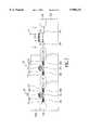
- FIG. 1shows a cross sectional view of a substrate having a PMOS, NMOS region and a ESD protective region in accordance with the present invention
- FIG. 2shows the formation of lightly doped drain (LDD) regions in the NMOS device in accordance with the present invention
- FIG. 3shows the formation of LDD regions in the PMOS device in accordance with the present invention
- FIG. 4shows that dopants are implanted into the NMOS device to form source/drain regions in accordance with the present invention
- FIG. 5shows that dopants are implanted into the PMOS device to form source/drain regions in accordance with the present invention
- FIG. 6shows the formation of a silicide layer on the gate, drain/source regions and the ESD region in accordance with the present invention
- FIG. 7shows the definition of the gate structure and the source/drain regions in the ESD protective region in accordance with the present invention.
- FIG. 8shows a schematic cross-sectional view of a substrate, which is covered by a thick oxide layer, and then a high temperature O 2 anneal process is performed.
- the present inventionproposes a simple method to fabricate the non-silicided region for ESD protection circuits with no additional mask.
- the ESD protection deviceis protected by a polysilicon layer, which is formed during the definition of the gate of the peripheral circuits.
- the polysilicon layeris used to be a hard mask for the ESD protective device during a salicide process for peripheral circuit.
- the salicide layeris formed on the active region of the peripheral circuits but not on the source/drain regions of the ESD protective device.
- a single crystal P-type substrate 100 with a ⁇ 100> crystallographic orientationis used for the preferred embodiment.
- a thick field oxide region (FOX) 102is created using conventional methods for the purposes of isolation.
- the FOX 110 regionis created via photolithography and dry etching steps to etch a silicon nitride/silicon dioxide composite layer. After the photoresist is removed and wet cleaned, a thermal oxidation in an oxygen-steam ambient is used to form the FOX 110 region, to a thickness of about 3000 to 8000 angstroms.
- an ESD protective region 10NMOS region 20 and PMOS region 30 are defined on the substrate 100.
- a gate oxide 220 and 230are defined atop NMOS region 20 and PMOS region 30, respectively.
- a gate 130, 230 and 330are defined on the gate oxide of the NMOS region 20 and PMOS region 30.
- the gate oxideis formed by using an oxygen-steam ambient.
- the gate oxidemay be formed using other known oxide chemical composition and procedures.
- the thickness of the gate oxide layeris approximately 30 to 200 angstroms.
- the gate electrodeis consequently formed from polysilicon material.
- the polysiliconcan be formed by using low pressure chemical vapor deposition (LPCVD) process, using silane as a source.
- the thickness of the polysilicon layeris approximately 1000 to 5000 angstroms.
- a silicon oxide layer 120 and a polysilicon layer 130are formed on the ESD protective region 10.
- the polysilicon layer 130is used to be a protective layer of the ESD protective region 10.
- a photoresist layer 1000is formed on the PMOS regions 30 and an ion implantation is applied to form N-LDD regions 240 in the NMOS region 20.
- N-type dopantsare implanted using the polysilicon layer 130 and photoresist layer 1000 as masks into the ESD protective region 10 and the NMOS region 20, simultaneously.
- the substrate 100 below the polysilicon layer 130is not doped.
- a lithography process for protecting the ESD protective region 10is omitted.
- the ion implantation containing N-type dopantsis performed with a dosage between about 5 ⁇ 10 12 to 5 ⁇ 10 14 ions/cm 2 , at an energy between about 10 to 80 KeV.
- the photoresist layer 1000is removed by using a conventional technology.
- a photoresist layer 1100is defined on the ESD protective region 10 and the NMOS region 20 to expose the PMOS region 30 exposed.
- a P-LDD implantationis then performed to form P-LDD region 340 in the PMOS region 30.
- the P-type dopantis typically boron ion and the implantation is performed with a dose between about 5 ⁇ 10 12 to 5 ⁇ 10 14 ions/cm 2 , at an energy between about 5 to 60 KeV.
- the photoresist layer 1100is stripped.
- spacers 150 of the polysilicon layer 130, spacers 250 of the gate 230, spacers 350 of the gate 330are formed by using the definition of a silicon oxide layer.
- a photoresist layer 1200is defined to protect the PMOS region 30.
- an ion implantation containing N-type dopantsis used to form source/drain regions 260 in the NMOS region 20, as shown in FIG. 4, by using the photoresist layer 1200 as the hard mask of the PMOS region 30.
- the polysilicon layer 130acts as a mask to prevent the ESD region 130 from doping.
- the ion implantation for forming the source/drain regions 260is applied with a dose between about 5 ⁇ 10 14 to 5 ⁇ 10 16 ions/cm 2 , at an energy between about 0.1 to 60 KeV.
- the photoresist layer 1200is stripped after that the implantation process is done.
- a photoresist layer 1300is created by lithography process on the ESD protective region 10 and the NMOS region 20.
- the PMOS region 30is doped to form source/drain regions 360 by doped the substrate 100 behind the spacers 350.
- a dose of dopantsbetween about 5 ⁇ 10 14 to 5 ⁇ 10 16 ions/cm 2 , at an energy between about 0.1 to 60 KeV, is used to form the source/drain region 360.
- a self-aligned silicided processis done to form salicide layers.
- a refractory or noble metalis deposited on the entire region by using physical vapor deposition (PVD) process or chemical vapor deposition (CVD) process and it is typically formed of Ti, W, Co, Ni, Cr, Pd and Pt, etc.
- PVDphysical vapor deposition
- CVDchemical vapor deposition
- RTArapid thermal annealing
- the first RTA processis done at a temperature between about 300 to 700 degrees centigrade and the second RTA process has an annealing temperature between about 750 to 1050 degrees centigrade.
- the unreacted metal layer during the first RTA processis removed in a room temperature mixture of DI H 2 O, H 2 O 2 and NH 4 OH at a ratio 5:1:1, a second RTA process is used to lower the sheet resistance of the silicide layer, and to stabilize the phase of silicide layers.
- the polysilicon layer 130 and the silicon oxide layer 120are anisotropically etched back to define a gate oxide 121 and a gate 131 of the ESD protective device 10, and the substrate 100 behind the gate 131 exposes.
- High dose arsenic and/or phosphorus ionsare implanted into the ESD protective region 10 to form the source/drain region 180.
- the implantation processis done with a dose between about 5 ⁇ 10 14 to 5 ⁇ 10 16 ions/cm 2 , at an energy between about 0.5 to 120 KeV.
- a photoresist layer 1400is used to prevent the NMOS region 20 and the PMOS region 30 from be doped. Afterwards, the photoresist layer 1400 is stripped by using conventional lithography technique.
- a thick CVD oxide layer 190like TESO-oxide or BPSG, is deposited on all region.
- the CVD oxide layer 190has a thickness between about 3000 to 8000 angstroms.
- a high temperature O 2 annealing processis used to densify the CVD oxide layer 190.
- the circuit operation speedcould be significantly improved due to the NMOS and PMOS device having source/drain and gate regions with silicide layers.
- the device with a silicided contacthas a faster operation speed than that of a conventional device.
- a higher ESD protective voltagecould be obtained as the ESD device has non-silicided source/drain regions.
- the proposed recipe of the present inventiondo not need a mask to block the ESD protective device during the salicidation process of the peripheral circuits.
Landscapes
- Metal-Oxide And Bipolar Metal-Oxide Semiconductor Integrated Circuits (AREA)
- Insulated Gate Type Field-Effect Transistor (AREA)
Abstract
Description
Claims (20)
Priority Applications (1)
| Application Number | Priority Date | Filing Date | Title |
|---|---|---|---|
| US09/057,866US5998247A (en) | 1998-04-09 | 1998-04-09 | Process to fabricate the non-silicide region for electrostatic discharge protection circuit |
Applications Claiming Priority (1)
| Application Number | Priority Date | Filing Date | Title |
|---|---|---|---|
| US09/057,866US5998247A (en) | 1998-04-09 | 1998-04-09 | Process to fabricate the non-silicide region for electrostatic discharge protection circuit |
Publications (1)
| Publication Number | Publication Date |
|---|---|
| US5998247Atrue US5998247A (en) | 1999-12-07 |
Family
ID=22013204
Family Applications (1)
| Application Number | Title | Priority Date | Filing Date |
|---|---|---|---|
| US09/057,866Expired - LifetimeUS5998247A (en) | 1998-04-09 | 1998-04-09 | Process to fabricate the non-silicide region for electrostatic discharge protection circuit |
Country Status (1)
| Country | Link |
|---|---|
| US (1) | US5998247A (en) |
Cited By (17)
| Publication number | Priority date | Publication date | Assignee | Title |
|---|---|---|---|---|
| US6156593A (en)* | 1998-03-30 | 2000-12-05 | United Microelectronics Corp. | Method for fabricating salicide CMOS and non-salicide electrostatic discharge protection circuit in a single chip |
| US6207492B1 (en) | 2000-06-05 | 2001-03-27 | Taiwan Semiconductor Manufacturing Company | Common gate and salicide word line process for low cost embedded DRAM devices |
| US6268241B1 (en)* | 1999-09-29 | 2001-07-31 | United Microelectronics Corp. | Method of forming a self-aligned silicide structure in integrated circuit fabrication |
| US20010015453A1 (en)* | 2000-02-23 | 2001-08-23 | Agarwal Vishnu K. | Capacitor forming methods |
| US6387788B2 (en)* | 1998-06-29 | 2002-05-14 | Hyundai Electronics Industries Co., Ltd. | Method for forming polycide gate electrode of metal oxide semiconductor field effect transistor |
| US20050045952A1 (en)* | 2003-08-27 | 2005-03-03 | International Business Machines Corporation | Pfet-based esd protection strategy for improved external latch-up robustness |
| US20050067658A1 (en)* | 2003-09-26 | 2005-03-31 | Akira Takahashi | Dry etching method for semiconductor device |
| US6891217B1 (en) | 1998-04-10 | 2005-05-10 | Micron Technology, Inc. | Capacitor with discrete dielectric material |
| US20070295357A1 (en)* | 2006-06-27 | 2007-12-27 | Lovejoy Michael L | Removing metal using an oxidizing chemistry |
| CN100452392C (en)* | 2003-05-22 | 2009-01-14 | 统宝光电股份有限公司 | Electrostatic discharge protection element with thick film polysilicon, electronic device and manufacturing method |
| US20110156164A1 (en)* | 2008-07-18 | 2011-06-30 | Renesas Electronics Corporation | Semiconductor device and method of manufacturing the same |
| CN102437116A (en)* | 2011-09-23 | 2012-05-02 | 上海华力微电子有限公司 | Process integration method for effectively reducing area of electrostatic discharge protection circuit |
| US8779551B2 (en) | 2012-06-06 | 2014-07-15 | International Business Machines Corporation | Gated diode structure for eliminating RIE damage from cap removal |
| US9918668B2 (en) | 2005-03-10 | 2018-03-20 | Dexcom, Inc. | System and methods for processing analyte sensor data for sensor calibration |
| US10524703B2 (en) | 2004-07-13 | 2020-01-07 | Dexcom, Inc. | Transcutaneous analyte sensor |
| US10813577B2 (en) | 2005-06-21 | 2020-10-27 | Dexcom, Inc. | Analyte sensor |
| US20240405015A1 (en)* | 2023-06-05 | 2024-12-05 | HeFeChip Corporation Limited | Semiconductor device with esd protection structure and method of making same |
Citations (5)
| Publication number | Priority date | Publication date | Assignee | Title |
|---|---|---|---|---|
| US4717684A (en)* | 1985-02-01 | 1988-01-05 | Hitachi, Ltd. | Semiconductor integrated circuit device |
| US5529941A (en)* | 1994-03-28 | 1996-06-25 | Vlsi Technology, Inc. | Method for making an integrated circuit structure |
| US5532178A (en)* | 1995-04-27 | 1996-07-02 | Taiwan Semiconductor Manufacturing Company | Gate process for NMOS ESD protection circuits |
| US5589423A (en)* | 1994-10-03 | 1996-12-31 | Motorola Inc. | Process for fabricating a non-silicided region in an integrated circuit |
| US5672527A (en)* | 1996-03-08 | 1997-09-30 | United Microelectronics Corp. | Method for fabricating an electrostatic discharge protection circuit |
- 1998
- 1998-04-09USUS09/057,866patent/US5998247A/ennot_activeExpired - Lifetime
Patent Citations (5)
| Publication number | Priority date | Publication date | Assignee | Title |
|---|---|---|---|---|
| US4717684A (en)* | 1985-02-01 | 1988-01-05 | Hitachi, Ltd. | Semiconductor integrated circuit device |
| US5529941A (en)* | 1994-03-28 | 1996-06-25 | Vlsi Technology, Inc. | Method for making an integrated circuit structure |
| US5589423A (en)* | 1994-10-03 | 1996-12-31 | Motorola Inc. | Process for fabricating a non-silicided region in an integrated circuit |
| US5532178A (en)* | 1995-04-27 | 1996-07-02 | Taiwan Semiconductor Manufacturing Company | Gate process for NMOS ESD protection circuits |
| US5672527A (en)* | 1996-03-08 | 1997-09-30 | United Microelectronics Corp. | Method for fabricating an electrostatic discharge protection circuit |
Cited By (58)
| Publication number | Priority date | Publication date | Assignee | Title |
|---|---|---|---|---|
| US6156593A (en)* | 1998-03-30 | 2000-12-05 | United Microelectronics Corp. | Method for fabricating salicide CMOS and non-salicide electrostatic discharge protection circuit in a single chip |
| US6891217B1 (en) | 1998-04-10 | 2005-05-10 | Micron Technology, Inc. | Capacitor with discrete dielectric material |
| US7166885B2 (en) | 1998-04-10 | 2007-01-23 | Micron Technology, Inc. | Semiconductor devices |
| US6995419B2 (en) | 1998-04-10 | 2006-02-07 | Micron Technology, Inc. | Semiconductor constructions having crystalline dielectric layers |
| US6387788B2 (en)* | 1998-06-29 | 2002-05-14 | Hyundai Electronics Industries Co., Ltd. | Method for forming polycide gate electrode of metal oxide semiconductor field effect transistor |
| US6268241B1 (en)* | 1999-09-29 | 2001-07-31 | United Microelectronics Corp. | Method of forming a self-aligned silicide structure in integrated circuit fabrication |
| US20010015453A1 (en)* | 2000-02-23 | 2001-08-23 | Agarwal Vishnu K. | Capacitor forming methods |
| US6953721B2 (en) | 2000-02-23 | 2005-10-11 | Micron Technology, Inc. | Methods of forming a capacitor with an amorphous and a crystalline high K capacitor dielectric region |
| US7005695B1 (en)* | 2000-02-23 | 2006-02-28 | Micron Technology, Inc. | Integrated circuitry including a capacitor with an amorphous and a crystalline high K capacitor dielectric region |
| US7446363B2 (en)* | 2000-02-23 | 2008-11-04 | Micron Technology, Inc. | Capacitor including a percentage of amorphous dielectric material and a percentage of crystalline dielectric material |
| US6207492B1 (en) | 2000-06-05 | 2001-03-27 | Taiwan Semiconductor Manufacturing Company | Common gate and salicide word line process for low cost embedded DRAM devices |
| CN100452392C (en)* | 2003-05-22 | 2009-01-14 | 统宝光电股份有限公司 | Electrostatic discharge protection element with thick film polysilicon, electronic device and manufacturing method |
| US20050045952A1 (en)* | 2003-08-27 | 2005-03-03 | International Business Machines Corporation | Pfet-based esd protection strategy for improved external latch-up robustness |
| US20050067658A1 (en)* | 2003-09-26 | 2005-03-31 | Akira Takahashi | Dry etching method for semiconductor device |
| US7955963B2 (en)* | 2003-09-26 | 2011-06-07 | Oki Semiconductor Co., Ltd. | Dry etching method for semiconductor device |
| US10709362B2 (en) | 2004-07-13 | 2020-07-14 | Dexcom, Inc. | Analyte sensor |
| US10799158B2 (en) | 2004-07-13 | 2020-10-13 | Dexcom, Inc. | Analyte sensor |
| US11883164B2 (en) | 2004-07-13 | 2024-01-30 | Dexcom, Inc. | System and methods for processing analyte sensor data for sensor calibration |
| US11064917B2 (en) | 2004-07-13 | 2021-07-20 | Dexcom, Inc. | Analyte sensor |
| US11045120B2 (en) | 2004-07-13 | 2021-06-29 | Dexcom, Inc. | Analyte sensor |
| US11026605B1 (en) | 2004-07-13 | 2021-06-08 | Dexcom, Inc. | Analyte sensor |
| US10993641B2 (en) | 2004-07-13 | 2021-05-04 | Dexcom, Inc. | Analyte sensor |
| US10524703B2 (en) | 2004-07-13 | 2020-01-07 | Dexcom, Inc. | Transcutaneous analyte sensor |
| US10993642B2 (en) | 2004-07-13 | 2021-05-04 | Dexcom, Inc. | Analyte sensor |
| US10980452B2 (en) | 2004-07-13 | 2021-04-20 | Dexcom, Inc. | Analyte sensor |
| US10932700B2 (en) | 2004-07-13 | 2021-03-02 | Dexcom, Inc. | Analyte sensor |
| US10918315B2 (en) | 2004-07-13 | 2021-02-16 | Dexcom, Inc. | Analyte sensor |
| US10709363B2 (en) | 2004-07-13 | 2020-07-14 | Dexcom, Inc. | Analyte sensor |
| US10918313B2 (en) | 2004-07-13 | 2021-02-16 | Dexcom, Inc. | Analyte sensor |
| US10918314B2 (en) | 2004-07-13 | 2021-02-16 | Dexcom, Inc. | Analyte sensor |
| US10827956B2 (en) | 2004-07-13 | 2020-11-10 | Dexcom, Inc. | Analyte sensor |
| US10722152B2 (en) | 2004-07-13 | 2020-07-28 | Dexcom, Inc. | Analyte sensor |
| US10813576B2 (en) | 2004-07-13 | 2020-10-27 | Dexcom, Inc. | Analyte sensor |
| US10799159B2 (en) | 2004-07-13 | 2020-10-13 | Dexcom, Inc. | Analyte sensor |
| US10617336B2 (en) | 2005-03-10 | 2020-04-14 | Dexcom, Inc. | System and methods for processing analyte sensor data for sensor calibration |
| US10918317B2 (en) | 2005-03-10 | 2021-02-16 | Dexcom, Inc. | System and methods for processing analyte sensor data for sensor calibration |
| US10743801B2 (en) | 2005-03-10 | 2020-08-18 | Dexcom, Inc. | System and methods for processing analyte sensor data for sensor calibration |
| US10716498B2 (en) | 2005-03-10 | 2020-07-21 | Dexcom, Inc. | System and methods for processing analyte sensor data for sensor calibration |
| US10856787B2 (en) | 2005-03-10 | 2020-12-08 | Dexcom, Inc. | System and methods for processing analyte sensor data for sensor calibration |
| US10898114B2 (en) | 2005-03-10 | 2021-01-26 | Dexcom, Inc. | System and methods for processing analyte sensor data for sensor calibration |
| US10709364B2 (en) | 2005-03-10 | 2020-07-14 | Dexcom, Inc. | System and methods for processing analyte sensor data for sensor calibration |
| US10918318B2 (en) | 2005-03-10 | 2021-02-16 | Dexcom, Inc. | System and methods for processing analyte sensor data for sensor calibration |
| US11051726B2 (en) | 2005-03-10 | 2021-07-06 | Dexcom, Inc. | System and methods for processing analyte sensor data for sensor calibration |
| US11000213B2 (en) | 2005-03-10 | 2021-05-11 | Dexcom, Inc. | System and methods for processing analyte sensor data for sensor calibration |
| US10918316B2 (en) | 2005-03-10 | 2021-02-16 | Dexcom, Inc. | System and methods for processing analyte sensor data for sensor calibration |
| US9918668B2 (en) | 2005-03-10 | 2018-03-20 | Dexcom, Inc. | System and methods for processing analyte sensor data for sensor calibration |
| US10925524B2 (en) | 2005-03-10 | 2021-02-23 | Dexcom, Inc. | System and methods for processing analyte sensor data for sensor calibration |
| US10610135B2 (en) | 2005-03-10 | 2020-04-07 | Dexcom, Inc. | System and methods for processing analyte sensor data for sensor calibration |
| US10610136B2 (en) | 2005-03-10 | 2020-04-07 | Dexcom, Inc. | System and methods for processing analyte sensor data for sensor calibration |
| US10610137B2 (en) | 2005-03-10 | 2020-04-07 | Dexcom, Inc. | System and methods for processing analyte sensor data for sensor calibration |
| US10813577B2 (en) | 2005-06-21 | 2020-10-27 | Dexcom, Inc. | Analyte sensor |
| US20070295357A1 (en)* | 2006-06-27 | 2007-12-27 | Lovejoy Michael L | Removing metal using an oxidizing chemistry |
| US20110156164A1 (en)* | 2008-07-18 | 2011-06-30 | Renesas Electronics Corporation | Semiconductor device and method of manufacturing the same |
| US8507373B2 (en)* | 2008-07-18 | 2013-08-13 | Renesas Electronics Corporation | Semiconductor device including transistors of different junction depth, and method of manufacturing the same |
| CN102437116A (en)* | 2011-09-23 | 2012-05-02 | 上海华力微电子有限公司 | Process integration method for effectively reducing area of electrostatic discharge protection circuit |
| US9064972B2 (en) | 2012-06-06 | 2015-06-23 | International Business Machines Corporation | Method of forming a gated diode structure for eliminating RIE damage from cap removal |
| US8779551B2 (en) | 2012-06-06 | 2014-07-15 | International Business Machines Corporation | Gated diode structure for eliminating RIE damage from cap removal |
| US20240405015A1 (en)* | 2023-06-05 | 2024-12-05 | HeFeChip Corporation Limited | Semiconductor device with esd protection structure and method of making same |
Similar Documents
| Publication | Publication Date | Title |
|---|---|---|
| US5897348A (en) | Low mask count self-aligned silicided CMOS transistors with a high electrostatic discharge resistance | |
| US6528381B2 (en) | Method of forming silicide | |
| US5998247A (en) | Process to fabricate the non-silicide region for electrostatic discharge protection circuit | |
| US5464782A (en) | Method to ensure isolation between source-drain and gate electrode using self aligned silicidation | |
| US5930617A (en) | Method of forming deep sub-micron CMOS transistors with self-aligned silicided contact and extended S/D junction | |
| US7569457B2 (en) | Method of fabricating semiconductor device | |
| US5956584A (en) | Method of making self-aligned silicide CMOS transistors | |
| US6642119B1 (en) | Silicide MOSFET architecture and method of manufacture | |
| US6090653A (en) | Method of manufacturing CMOS transistors | |
| JP2004274022A (en) | Method of forming a high performance, low cost CMOS device | |
| US6593198B2 (en) | Semiconductor device and method for fabricating the same | |
| US6063706A (en) | Method to simulataneously fabricate the self-aligned silicided devices and ESD protective devices | |
| US20020123192A1 (en) | Selective salicide process by reformation of silicon nitride sidewall spacers | |
| US6020240A (en) | Method to simultaneously fabricate the self-aligned silicided devices and ESD protection devices | |
| US6121090A (en) | Self-aligned silicided MOS devices with an extended S/D junction and an ESD protection circuit | |
| WO1999016116A1 (en) | Method for manufacturing semiconductor device | |
| JPH08213610A (en) | Field effect type semiconductor device and method of manufacturing the same | |
| KR100658088B1 (en) | Low leakage mos transistor | |
| US5747852A (en) | LDD MOS transistor with improved uniformity and controllability of alignment | |
| US6278160B1 (en) | Semiconductor device having a reliably-formed narrow active region | |
| US6635539B2 (en) | Method for fabricating a MOS transistor using a self-aligned silicide technique | |
| US20030111689A1 (en) | Process for the selective formation of salicide on active areas of MOS devices | |
| US7709911B2 (en) | Semiconductor device having silicide transistors and non-silicide transistors formed on the same substrate and method for fabricating the same | |
| KR100353550B1 (en) | Silicide and forming method thereof | |
| JPH0964349A (en) | Semiconductor device with high-melting-point silicide and its manufacture |
Legal Events
| Date | Code | Title | Description |
|---|---|---|---|
| AS | Assignment | Owner name:TEXAS INSTRUMENTS - ACER INCORPORATED, TAIWAN Free format text:ASSIGNMENT OF ASSIGNORS INTEREST;ASSIGNOR:WU, SHYE-LIN;REEL/FRAME:009096/0913 Effective date:19980327 | |
| STCF | Information on status: patent grant | Free format text:PATENTED CASE | |
| AS | Assignment | Owner name:TSMC-ACER SEMICONDUCTOR MANUFACTURING CORPORATION, Free format text:ASSIGNMENT OF ASSIGNORS INTEREST;ASSIGNOR:ACER SEMICONDUCTOR MANUFACTURING INC.;REEL/FRAME:011087/0473 Effective date:20000630 Owner name:TAIWAN SEMICONDUCTOR MANUFACTURING CO., LTD., TAIW Free format text:ASSIGNMENT OF ASSIGNORS INTEREST;ASSIGNOR:TSMC-ACER SEMICONDUCTOR MANUFACTURING CORPORATION;REEL/FRAME:011122/0153 Effective date:20000630 | |
| FEPP | Fee payment procedure | Free format text:PAYER NUMBER DE-ASSIGNED (ORIGINAL EVENT CODE: RMPN); ENTITY STATUS OF PATENT OWNER: LARGE ENTITY Free format text:PAYOR NUMBER ASSIGNED (ORIGINAL EVENT CODE: ASPN); ENTITY STATUS OF PATENT OWNER: LARGE ENTITY | |
| FPAY | Fee payment | Year of fee payment:4 | |
| FPAY | Fee payment | Year of fee payment:8 | |
| FPAY | Fee payment | Year of fee payment:12 |