US5997384A - Method and apparatus for controlling planarizing characteristics in mechanical and chemical-mechanical planarization of microelectronic substrates - Google Patents
Method and apparatus for controlling planarizing characteristics in mechanical and chemical-mechanical planarization of microelectronic substratesDownload PDFInfo
- Publication number
- US5997384A US5997384AUS08/995,493US99549397AUS5997384AUS 5997384 AUS5997384 AUS 5997384AUS 99549397 AUS99549397 AUS 99549397AUS 5997384 AUS5997384 AUS 5997384A
- Authority
- US
- United States
- Prior art keywords
- substrate
- standing wave
- modulator
- contact element
- actuator
- Prior art date
- Legal status (The legal status is an assumption and is not a legal conclusion. Google has not performed a legal analysis and makes no representation as to the accuracy of the status listed.)
- Ceased
Links
- 239000000758substrateSubstances0.000titleclaimsabstractdescription382
- 238000004377microelectronicMethods0.000titleclaimsabstractdescription86
- 238000000034methodMethods0.000titleclaimsabstractdescription44
- 238000005498polishingMethods0.000claimsabstractdescription116
- 238000004519manufacturing processMethods0.000claimsdescription14
- 238000003825pressingMethods0.000claims9
- 230000003068static effectEffects0.000claims8
- 239000002245particleSubstances0.000description6
- 239000002002slurrySubstances0.000description6
- 230000000694effectsEffects0.000description4
- 239000000463materialSubstances0.000description4
- 235000012431wafersNutrition0.000description4
- 238000009826distributionMethods0.000description3
- 239000004065semiconductorSubstances0.000description3
- 239000000126substanceSubstances0.000description3
- 238000006073displacement reactionMethods0.000description2
- 239000004814polyurethaneSubstances0.000description2
- 229920002635polyurethanePolymers0.000description2
- 239000000919ceramicSubstances0.000description1
- 230000002860competitive effectEffects0.000description1
- 230000002950deficientEffects0.000description1
- 239000007788liquidSubstances0.000description1
- 239000011159matrix materialSubstances0.000description1
- 239000002184metalSubstances0.000description1
- 238000012986modificationMethods0.000description1
- 230000004048modificationEffects0.000description1
- 238000009828non-uniform distributionMethods0.000description1
- 239000007787solidSubstances0.000description1
- 239000000725suspensionSubstances0.000description1
Images


Classifications
- B—PERFORMING OPERATIONS; TRANSPORTING
- B24—GRINDING; POLISHING
- B24B—MACHINES, DEVICES, OR PROCESSES FOR GRINDING OR POLISHING; DRESSING OR CONDITIONING OF ABRADING SURFACES; FEEDING OF GRINDING, POLISHING, OR LAPPING AGENTS
- B24B37/00—Lapping machines or devices; Accessories
- B24B37/04—Lapping machines or devices; Accessories designed for working plane surfaces
- B24B37/07—Lapping machines or devices; Accessories designed for working plane surfaces characterised by the movement of the work or lapping tool
- B24B37/10—Lapping machines or devices; Accessories designed for working plane surfaces characterised by the movement of the work or lapping tool for single side lapping
- B24B37/105—Lapping machines or devices; Accessories designed for working plane surfaces characterised by the movement of the work or lapping tool for single side lapping the workpieces or work carriers being actively moved by a drive, e.g. in a combined rotary and translatory movement
- B—PERFORMING OPERATIONS; TRANSPORTING
- B24—GRINDING; POLISHING
- B24B—MACHINES, DEVICES, OR PROCESSES FOR GRINDING OR POLISHING; DRESSING OR CONDITIONING OF ABRADING SURFACES; FEEDING OF GRINDING, POLISHING, OR LAPPING AGENTS
- B24B21/00—Machines or devices using grinding or polishing belts; Accessories therefor
- B24B21/004—Machines or devices using grinding or polishing belts; Accessories therefor using abrasive rolled strips
- B—PERFORMING OPERATIONS; TRANSPORTING
- B24—GRINDING; POLISHING
- B24B—MACHINES, DEVICES, OR PROCESSES FOR GRINDING OR POLISHING; DRESSING OR CONDITIONING OF ABRADING SURFACES; FEEDING OF GRINDING, POLISHING, OR LAPPING AGENTS
- B24B37/00—Lapping machines or devices; Accessories
- B24B37/27—Work carriers
- B24B37/30—Work carriers for single side lapping of plane surfaces
- B—PERFORMING OPERATIONS; TRANSPORTING
- B24—GRINDING; POLISHING
- B24B—MACHINES, DEVICES, OR PROCESSES FOR GRINDING OR POLISHING; DRESSING OR CONDITIONING OF ABRADING SURFACES; FEEDING OF GRINDING, POLISHING, OR LAPPING AGENTS
- B24B49/00—Measuring or gauging equipment for controlling the feed movement of the grinding tool or work; Arrangements of indicating or measuring equipment, e.g. for indicating the start of the grinding operation
Definitions
- the present inventionrelates to mechanical and chemical-mechanical planarization of microelectronic substrates. More particularly, the present invention relates to controlling the planarizing characteristics of a microelectronic substrate.
- FIG. 1schematically illustrates a planarizing machine 10 with a platen or base 20, a carrier assembly 30, a polishing pad 40, and a planarizing solution 44 on the polishing pad 40.
- the planarizing machine 10may also have an under-pad 25 attached to an upper surface 22 of the platen 20 for supporting the polishing pad 40.
- a drive assembly 26rotates (arrow A) and/or reciprocates (arrow B) the platen 20 to move the polishing pad 40 during planarization.
- the carrier assembly 30controls and protects a substrate 12 during planarization.
- the carrier assembly 30generally has a substrate holder 32 with a pad 34 that holds the substrate 12 via suction, and an actuator assembly 36 typically rotates and/or translates the substrate holder 32 (arrows C and D, respectively).
- the substrate holder 32may be a weighted, free-floating disk (not shown) that slides over the polishing pad 40.
- the polishing pad 40 and the planarizing solution 44may separately, or in combination, define a polishing environment that mechanically and/or chemically removes material from the surface of the substrate 12.
- the polishing pad 40may be a conventional polishing pad made from a relatively compressible, porous continuous phase matrix material (e.g., polyurethane), or it may be an abrasive polishing pad with abrasive particles fixedly bonded to a suspension medium.
- the planarizing solution 44may be a chemical-mechanical planarization slurry with abrasive particles and chemicals for use with a conventional non-abrasive polishing pad, or the planarizing solution 44 may be a liquid without abrasive particles for use with an abrasive polishing pad.
- the carrier assembly 30presses the substrate 12 against a planarizing surface 42 of the polishing pad 40 in the presence of the planarizing solution 44.
- the platen 20 and/or the substrate holder 32then move relative to one another to translate the substrate 12 across the planarizing surface 42.
- the abrasive particles and/or the chemicals in the polishing environmentremove material from the surface of the substrate 12.
- Planarizing processesmust consistently and accurately produce a uniformly planar surface on the substrate to enable precise fabrication of circuits and photo-patterns on the substrate.
- the uniformity and planarity of the substrate surfaceis becoming increasingly important because it is difficult to form sub-micron features or photo-patterns to within a tolerance of approximately 0.1 ⁇ m when the substrate surface is not uniformly planar.
- planarizing processesmust create a highly uniform, planar surface on the substrate.
- Typical semiconductor manufacturing processesfabricate a plurality of dies (e.g., 50-250) on each substrate.
- diese.g., 50-250
- planarizing processesshould form a planar surface across the substrate surface.
- the substrate surfacemay not be uniformly planar because the rate at which material is removed from the substrate surface (the "polishing rate") typically varies from one region on the substrate to another.
- the polishing rateis a function of several factors, and many of the factors may change throughout the planarizing process. For example, some of the factors that effect the polishing rate across the surface of the substrate are as follows: (1) the distribution of abrasive particles and chemicals between the substrate surface and the polishing pad; (2) the relative velocity between the polishing pad and the substrate surface; and (3) the pressure distribution across the substrate surface.
- planarizing devices and methodstypically produce a non-uniform, center-to-edge planarizing profile across the substrate surface.
- a Rodel IC-1000 polishing padis a relatively soft, porous polyurethane pad with a number of large slurry wells approximately 0.05-0.10 inches in diameter that are spaced apart from one another across the planarizing surface by approximately 0.125-0.25 inches.
- small volumes of slurryare expected to fill the large wells, and then hydrodynamic forces created by the motion of the substrate are expected to draw the slurry out of the wells in a manner that wets the substrate surface.
- U.S. Pat. No. 5,216,843describes another polishing pad with a plurality of macro-grooves formed in concentric circles and a plurality of micro-grooves radially crossing the macro-grooves. Although grooved pads may improve the planarity of the substrate surface, substrates planarized with such pads still exhibit non-uniformities across the substrate surface indicating a non-uniform distribution of planarizing solution and abrasive particles under the substrate.
- the deviation of the surface uniformity in the perimeter regionmay be so great that it impairs or ruins dies formed in the perimeter region.
- the center-to-edge planarizing profilesignificantly impacts the yield of larger substrates.
- an apparatus for controlling the planarizing characteristics of a microelectronic substratehas a carrier that may be positioned with respect to a polishing medium of a planarizing machine.
- the carriermay be a substrate holder of the planarizing machine or another carrier independent from the substrate holder that moves with respect to a microelectronic substrate during planarization of the substrate.
- the apparatusmay also have a modulator attached to the carrier, and the modulator may have a contact element for engaging the polishing medium.
- the modulatormay be attached to the carrier to position at least a portion of the contact element in front of a leading edge of the substrate by a selected distance during planarization.
- the contact elementselectively engages a portion of the planarizing surface proximate to the leading edge of the substrate to modulate the contour of the planarizing surface of the polishing medium.
- the modulatoris attached to the substrate holder to position the contact element superadjacent to an exposed portion of a standing wave that forms at the leading edge of the substrate during planarization.
- the contact elementoperates by engaging the exposed portion of the standing wave in a manner that modulates the contour of a residual portion of the standing wave under a perimeter region of the substrate.
- the modulatormay be a passive modulator in which the contact element has a bottom surface with a desired contour to attenuate or shift the residual portion of the standing wave.
- the modulatormay be an active modulator having an actuator that carries the contact element and a controller coupled to the actuator.
- the controllermay be programmed to drive the actuator in a manner that selectively moves a bottom surface of the contact element against the exposed portion of the standing wave.
- the particular motion of the actuatormay be selected to continually shift a pressure point of the residual portion of the standing wave and/or attenuate the residual portion of the standing wave.
- the active modulatormay move the contact element against the exposed portion of the standing wave in a manner that oscillates a pressure point of the residual portion of the standing wave under the perimeter region of the substrate to average the effect of the pressure point over a larger surface area on the substrate.
- FIG. 1is a schematic view of a planarizing machine in accordance with the prior art.
- FIG. 2is a schematic view of a planarizing machine with a device for controlling the planarizing characteristics of a microelectronic substrate in accordance with an embodiment of the invention.
- FIG. 3is a partial schematic cross-sectional view of a planarizing machine with a device for controlling the planarizing characteristics of a microelectronic substrate in accordance with one embodiment of the invention.
- FIG. 4Ais a partial schematic cross-sectional view illustrating the one aspect of the operation of the device of FIG. 3.
- FIG. 4Bis a partial schematic cross-sectional view illustrating another aspect of the operation of the device of FIG. 3.
- FIG. 5Ais a partial schematic cross-sectional view of a planarizing machine with another device for controlling the planarizing characteristics of a microelectronic substrate in accordance with another embodiment of the invention.
- FIG. 5Bis a partial schematic cross-sectional view illustrating the operation of the device of FIG. 5A.
- the present inventionis an apparatus and method for mechanical and/or chemical-mechanical planarization of substrates used in the manufacturing of microelectronic devices. Many specific details of certain embodiments of the invention are set forth in the following description and in FIGS. 2-5B to provide a thorough understanding of such embodiments. One skilled in the art, however, will understand that the present invention may have additional embodiments and may be practiced without several of the details described in the following description.
- FIG. 2is a schematic view of a planarizing machine 100 in accordance with one embodiment of the invention.
- the planarizing machine 100includes a carrier assembly 130 and an active modulator 170 for controlling the planarizing characteristics of a microelectronic substrate 12.
- the features and advantages of the modulator 170are best understood in the context of the structure and operation of the planarizing machine 100. Thus, the general features of the planarizing machine 100 will be described initially.
- the planarizing machine 100may have a platen or a support table 110 carrying an underpart 112 at a work station or a planarization station where a section "A" of a planarizing medium 100 is positioned.
- the underpart 112may be a substantially incompressible support member attached to the table 110 to provide a flat, solid surface to which a particular section of the polishing medium 140 may be secured during planarization. In other applications, however, the underpart 112 may be a compressible pad to provide a more conformal polishing medium.
- the planarizing machine 110also has a plurality of rollers to guide, position, and hold the polishing medium 140 over the underpart 112.
- the rollersinclude a supply roller 120, first and second idler rollers 121a and 121b, first and second guide rollers 122a and 122b, and a take-up roller 123.
- the supply roller 120carries an unused portion of the polishing medium 140
- the take-up roller 123carries the used portion of the polishing medium 140.
- the supply roller 120 and the take-up roller 123are driven rollers to sequentially advance the unused portion of the polishing medium 140 onto the underpart 112. As such, an unused section of the planarizing medium may be quickly substituted for a worn, used section to provide a consistent surface for planarizing the substrate.
- the first idler roller 121a and the first guide roller 122aposition the polishing medium 140 slightly below the underpart 112 so that the supply and take-up rollers 120 and 123 stretch the polishing medium 140 over the underpart 112 to hold it stationary during planarization.
- the planarizing machine 100also has a carrier assembly 130 to translate the substrate 12 across a planarizing surface 150 of the polishing medium 140.
- the carrier assembly 130has a substrate holder 132 to pick up, hold and release the substrate 12 at appropriate stages of the planarization process.
- the carrier assembly 130may also have a support gantry 134 carrying an actuator 136 so that the actuator 136 can translate along the gantry 134.
- the actuator 136preferably has a drive shaft 137 coupled to an arm assembly 138 that carries the substrate holder 132. In operation, the gantry 134 raises and lowers the substrate 12, and the actuator 136 orbits the substrate 12 about an axis B-B via the drive shaft 137.
- the arm assembly 138may also have an actuator (not shown) to drive a shaft 139 of the arm assembly 138 and thus rotate the substrate holder 132 about an axis C--C in addition to orbiting the substrate holder 132 about the axis B--B.
- the modulator 170may be an active modulator 170 with a contact element 172, an actuator 174 carrying the contact element 172, and a controller 180 coupled to the actuator 174.
- the actuator 174is attached to the substrate holder 132 to position at least a portion of the contact element 172 in front of leading edge of the substrate 12 during planarization.
- the actuator 174 and the contact element 172may surround the substrate 12 so that a portion of the contact element 172 is positioned superadjacent to an area on the polishing medium 140 in front of a leading edge of the substrate 12 irrespective of the direction that the substrate holder 132 is moving.
- the contact element 172may accordingly be a carrier ring that contains the substrate 12 within the substrate holder 132.
- the contact element 172selectively engages the planarizing surface 150 to modulate the contour of the planarizing surface 150 under a perimeter region of the substrate 12.
- FIG. 3is a partial schematic cross-sectional view of the substrate holder 132 showing a portion of the active modulator 170 in greater detail.
- the actuator 174may be a single linear displacement device or a plurality of displacement devices embedded in the substrate holder 132 in a ring around the substrate 12.
- the contact element 172may thus be a ring configured to position a bottom surface 173 of the contact element 172 superadjacent to a portion of the planarizing surface 150.
- the actuator 174is a piezoelectric ring driven by electric signals from the controller 180.
- the contact element 172may accordingly be a metal, ceramic or other type of ring attached to the piezoelectric actuator 174.
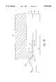
- One aspect of the inventionis the discovery that a leading edge 14 of the substrate 12 having a motion "M" forms a standing wave 152 in the planarizing surface 150 of the polishing medium 140.
- the particular waveform of the standing wave 152is a function of several factors, such as the pad type, substrate structure, planarizing solution, downforce, relative velocity and other factors.
- the standing wave 152 shown in FIG. 3is a schematic representation of a standing wave that does not necessarily represent the waveform of an actual standing wave. As such, the amplitude and wave length of the standing wave 152 shown in FIG. 3 are exaggerated for illustrative purposes.
- a planarizing solutionis not shown on top of the planarizing surface 150 for purposes of clarity, but it will be appreciated that a planarizing solution is typically dispensed onto the planarizing surface 150 during planarization.
- the controller 180drives the actuator 174 to move the contact element 172 vertically and/or horizontally with respect to an exposed portion 154 of the standing wave 152.
- the actuator 174may hold a bottom surface 173 of the contact element 172 in engagement with the planarizing surface 150 (not shown in FIG. 3) at a set position with respect to the exposed portion 154 of the standing wave 152 to alter a residual portion of the standing wave 156 with respect to the substrate 12.
- the actuator 174may continuously move the contact element 172 in engagement with the planarizing surface 150 to continuously alter the contour of the planarizing surface 150 in a manner that produces a plurality of different waveforms on the planarizing surface 150 instead of the standing wave 152.
- the actuatormay move the contact element 172 into engagement with the planarizing surface 150 at a selected frequency, amplitude and phase with respect to the standing wave 152 to cancel the standing wave 152 on the planarizing surface 150.
- the controller 180may be programmed to selectively operate the active modulator 170 in a desired manner according to the particular application.
- FIG. 4Ais a schematic partial cross-sectional view illustrating the aforementioned possible application in which the contact element 170 is held at a set position against the planarizing surface 150.
- the controller 180drives the actuator 174 to position the bottom surface 173 of the contact element 172 a distance h 1 away from a reference height ho where the bottom surface 173 engages the exposed portion 154 of the standing wave 152.
- the actuator 174may hold the bottom surface 173 in this position such that the force exerted by the contact element 172 against the exposed portion 154 changes the residual portion 156 of the standing wave 152 with respect to the perimeter region 15 of the substrate 12.
- the contact element 172may be positioned to affect the boundary condition of the standing wave 152 in a manner that attenuates and/or changes the position of pressure points of the residual portion 156 with respect to the substrate 12.
- FIG. 4Bis another schematic cross-sectional view that, together with FIG. 4A, illustrates the aforementioned possible application in which the actuator 174 continuously moves the contact element 172 in engagement with the planarizing surface 150 to produce a plurality of different waveforms on the planarizing surface 150.
- the actuator 174may move the bottom surface 173 of the contact element 172 between the position h 1 (FIG. 4A) and a position h 2 (FIG. 4B) at one or more frequencies to continuously alter the waveform on the planarizing surface.
- the standing wave 152 on the planarizing surface 150will be replaced by a number of different waves in which the pressure points act on different radial positions of the substrate 12.
- the actuator 174moves the contact element 172 from the position h 1 to the position h 2 during planarization, a number of pressure points 158 and 159 may move with respect to the substrate.
- the actuator 174accordingly, may move the contact element 172 during planarization to change the radial locations of the pressure points with respect to the substrate 12 so that the effects of the pressure points may be spread across a larger surface area of the substrate 12.
- the active modulator 170is expected to reduce the concentration of a high pressure forces at relatively fixed radial positions on the substrate 12.
- an operatormay measure the planarity of the perimeter region 15 of a number of substrates that were planarized while holding the contact element 172 at a number of different set positions or moving the contact element 172 at a number of selected frequencies and amplitudes. Since the shape of the standing wave 150 is a function of such factors as the pad type, substrate configuration, relative velocity, slurry distribution and down force, the particular position or movement of the contact element 172 may be determined empirically for each specific planarization process. Based upon the actual deviation in the surface uniformity of the perimeter region 15, and also based upon the size of the perimeter region 15, a person skilled in the art can determine the best position or motion of the contact element 172 to program into the controller 180.
- the planarizing machine 100 with the active modulator 170is expected to reduce the deviation in the surface uniformity in the perimeter region of a microelectronic substrate. Unlike conventional devices and methods for reducing the edge effect in planarization, several embodiments of the present invention are expected to enhance the uniformity of the substrate surface by altering the pressure exerted against the perimeter region of the substrate.
- the contact element 172more particularly, may shift and/or attenuate the residual portion of the standing wave under the perimeter region 15 of the substrate 12 to reduce the concentration of high pressure points at substantially fixed radial positions on the substrate 12.
- the modulator 170is expected to limit large deviations in the surface uniformity to a region approximately 2-5 mm from the substrate edge as opposed to the 5-15 mm perimeter region produced by conventional devices.
- the modulator 170is also expected to reduce the extent of the deviations in surface uniformity in the 2-5 mm perimeter region.
- the planarizing machine 100 with the active modulator 170is expected to increase the yield of operable dies on each substrate.
- FIGS. 5A and 5Bare partial schematic cross-sectional views of another embodiment of a modulator 270 for controlling the planarizing characteristics of microelectronic substrates.
- the modulator 270may be a passive modulator in which the contact element 272 is fixedly attached to or integrally formed with the substrate holder 132.
- the contact element 272may have a bottom surface 273 with a desired contour to modulate a residual portion 156 of the standing wave 152 on the planarizing surface 150 under the perimeter region 15 of the substrate 12.
- the contour of the bottom surface 273may be determined empirically to shift or attenuate the residual portion 156 of the standing wave.
- the shape of the bottom surface 273 shown in FIGS. 5A and 5Bis for illustrative purposes, and it will be appreciated that other shapes may be used to adapt the contact element 272 to the specific planarizing process.
- the width of the contact element 172 and its distance from the leading edge 14 of the substrate 12can also be determined empirically at different operating conditions such as wafer velocity.
- FIG. 5Billustrates the operation of the passive modulator 270 in which the substrate holder 132 presses the bottom surface 273 against the exposed portion 154 of the standing wave 152 on the planarizing surface 150.
- the shape of the bottom surface 273may be configured either to attenuate and/or shift the residual portion 156 of the standing wave 152.
- the passive modulator 270does not oscillate the pressure points of the residual portion 156 because the contact face 273 remains at the same elevation relative to the polishing pad 140 during planarization.
- the contact element 172may be an integral part of the piezoelectric actuator 174.
- the shape of the bottom surface 173 of the contact element 172may also be contoured as shown by the bottom surface 273 of the contact element 272. Accordingly, the invention is not limited except as by the appended claims.
Landscapes
- Engineering & Computer Science (AREA)
- Mechanical Engineering (AREA)
- Mechanical Treatment Of Semiconductor (AREA)
- Finish Polishing, Edge Sharpening, And Grinding By Specific Grinding Devices (AREA)
Abstract
Description
Claims (70)
Priority Applications (2)
| Application Number | Priority Date | Filing Date | Title |
|---|---|---|---|
| US08/995,493US5997384A (en) | 1997-12-22 | 1997-12-22 | Method and apparatus for controlling planarizing characteristics in mechanical and chemical-mechanical planarization of microelectronic substrates |
| US10/013,333USRE39194E1 (en) | 1997-12-22 | 2001-12-06 | Method and apparatus for controlling planarizing characteristics in mechanical and chemical-mechanical planarization of microelectronic substrates |
Applications Claiming Priority (1)
| Application Number | Priority Date | Filing Date | Title |
|---|---|---|---|
| US08/995,493US5997384A (en) | 1997-12-22 | 1997-12-22 | Method and apparatus for controlling planarizing characteristics in mechanical and chemical-mechanical planarization of microelectronic substrates |
Related Child Applications (1)
| Application Number | Title | Priority Date | Filing Date |
|---|---|---|---|
| US10/013,333ReissueUSRE39194E1 (en) | 1997-12-22 | 2001-12-06 | Method and apparatus for controlling planarizing characteristics in mechanical and chemical-mechanical planarization of microelectronic substrates |
Publications (1)
| Publication Number | Publication Date |
|---|---|
| US5997384Atrue US5997384A (en) | 1999-12-07 |
Family
ID=25541885
Family Applications (2)
| Application Number | Title | Priority Date | Filing Date |
|---|---|---|---|
| US08/995,493CeasedUS5997384A (en) | 1997-12-22 | 1997-12-22 | Method and apparatus for controlling planarizing characteristics in mechanical and chemical-mechanical planarization of microelectronic substrates |
| US10/013,333Expired - LifetimeUSRE39194E1 (en) | 1997-12-22 | 2001-12-06 | Method and apparatus for controlling planarizing characteristics in mechanical and chemical-mechanical planarization of microelectronic substrates |
Family Applications After (1)
| Application Number | Title | Priority Date | Filing Date |
|---|---|---|---|
| US10/013,333Expired - LifetimeUSRE39194E1 (en) | 1997-12-22 | 2001-12-06 | Method and apparatus for controlling planarizing characteristics in mechanical and chemical-mechanical planarization of microelectronic substrates |
Country Status (1)
| Country | Link |
|---|---|
| US (2) | US5997384A (en) |
Cited By (72)
| Publication number | Priority date | Publication date | Assignee | Title |
|---|---|---|---|---|
| WO2001005555A1 (en)* | 1999-07-20 | 2001-01-25 | Micron Technology, Inc. | Methods and apparatuses for planarizing microelectronic substrate assemblies |
| US6196899B1 (en)* | 1999-06-21 | 2001-03-06 | Micron Technology, Inc. | Polishing apparatus |
| US6213845B1 (en)* | 1999-04-26 | 2001-04-10 | Micron Technology, Inc. | Apparatus for in-situ optical endpointing on web-format planarizing machines in mechanical or chemical-mechanical planarization of microelectronic-device substrate assemblies and methods for making and using same |
| US6244935B1 (en)* | 1999-02-04 | 2001-06-12 | Applied Materials, Inc. | Apparatus and methods for chemical mechanical polishing with an advanceable polishing sheet |
| US6261162B1 (en)* | 1998-03-25 | 2001-07-17 | Ebara Corporation | Polishing apparatus and method of manufacturing grinding plate |
| US6277008B1 (en)* | 1998-04-10 | 2001-08-21 | Nec Corporation | Polishing apparatus |
| US6287185B1 (en)* | 1997-04-04 | 2001-09-11 | Rodel Holdings Inc. | Polishing pads and methods relating thereto |
| US6325696B1 (en)* | 1999-09-13 | 2001-12-04 | International Business Machines Corporation | Piezo-actuated CMP carrier |
| US6328632B1 (en)* | 1999-08-31 | 2001-12-11 | Micron Technology, Inc. | Polishing pads and planarizing machines for mechanical and/or chemical-mechanical planarization of microelectronic substrate assemblies |
| US6331135B1 (en)* | 1999-08-31 | 2001-12-18 | Micron Technology, Inc. | Method and apparatus for mechanical and chemical-mechanical planarization of microelectronic substrates with metal compound abrasives |
| US6398630B1 (en) | 1998-05-29 | 2002-06-04 | Micron Technology, Inc. | Planarizing machine containing web-format polishing pad and web-format polishing pads |
| US6413152B1 (en)* | 1999-12-22 | 2002-07-02 | Philips Electronics North American Corporation | Apparatus for performing chemical-mechanical planarization with improved process window, process flexibility and cost |
| US6419559B1 (en) | 2000-07-10 | 2002-07-16 | Applied Materials, Inc. | Using a purge gas in a chemical mechanical polishing apparatus with an incrementally advanceable polishing sheet |
| US6428386B1 (en) | 2000-06-16 | 2002-08-06 | Micron Technology, Inc. | Planarizing pads, planarizing machines, and methods for mechanical and/or chemical-mechanical planarization of microelectronic-device substrate assemblies |
| US6447369B1 (en) | 2000-08-30 | 2002-09-10 | Micron Technology, Inc. | Planarizing machines and alignment systems for mechanical and/or chemical-mechanical planarization of microelectronic substrates |
| US20020124958A1 (en)* | 2000-08-31 | 2002-09-12 | Blalock Guy T. | Methods and apparatuses for making and using planarizing pads for mechanical and chemical-mechanical planarization of microelectronic substrates |
| US6475070B1 (en)* | 1999-02-04 | 2002-11-05 | Applied Materials, Inc. | Chemical mechanical polishing with a moving polishing sheet |
| US6491570B1 (en)* | 1999-02-25 | 2002-12-10 | Applied Materials, Inc. | Polishing media stabilizer |
| US6498101B1 (en) | 2000-02-28 | 2002-12-24 | Micron Technology, Inc. | Planarizing pads, planarizing machines and methods for making and using planarizing pads in mechanical and chemical-mechanical planarization of microelectronic device substrate assemblies |
| US6511576B2 (en) | 1999-11-17 | 2003-01-28 | Micron Technology, Inc. | System for planarizing microelectronic substrates having apertures |
| US6520841B2 (en) | 2000-07-10 | 2003-02-18 | Applied Materials, Inc. | Apparatus and methods for chemical mechanical polishing with an incrementally advanceable polishing sheet |
| US6520834B1 (en) | 2000-08-09 | 2003-02-18 | Micron Technology, Inc. | Methods and apparatuses for analyzing and controlling performance parameters in mechanical and chemical-mechanical planarization of microelectronic substrates |
| US6533893B2 (en) | 1999-09-02 | 2003-03-18 | Micron Technology, Inc. | Method and apparatus for chemical-mechanical planarization of microelectronic substrates with selected planarizing liquids |
| US6548407B1 (en) | 2000-04-26 | 2003-04-15 | Micron Technology, Inc. | Method and apparatus for controlling chemical interactions during planarization of microelectronic substrates |
| US6579151B2 (en)* | 2001-08-02 | 2003-06-17 | Taiwan Semiconductor Manufacturing Co., Ltd | Retaining ring with active edge-profile control by piezoelectric actuator/sensors |
| US6592443B1 (en) | 2000-08-30 | 2003-07-15 | Micron Technology, Inc. | Method and apparatus for forming and using planarizing pads for mechanical and chemical-mechanical planarization of microelectronic substrates |
| US6609947B1 (en) | 2000-08-30 | 2003-08-26 | Micron Technology, Inc. | Planarizing machines and control systems for mechanical and/or chemical-mechanical planarization of micro electronic substrates |
| US6612901B1 (en) | 2000-06-07 | 2003-09-02 | Micron Technology, Inc. | Apparatus for in-situ optical endpointing of web-format planarizing machines in mechanical or chemical-mechanical planarization of microelectronic-device substrate assemblies |
| US6623329B1 (en) | 2000-08-31 | 2003-09-23 | Micron Technology, Inc. | Method and apparatus for supporting a microelectronic substrate relative to a planarization pad |
| US6628410B2 (en) | 1996-02-16 | 2003-09-30 | Micron Technology, Inc. | Endpoint detector and method for measuring a change in wafer thickness in chemical-mechanical polishing of semiconductor wafers and other microelectronic substrates |
| US6626744B1 (en) | 1999-12-17 | 2003-09-30 | Applied Materials, Inc. | Planarization system with multiple polishing pads |
| US20030224678A1 (en)* | 2002-05-31 | 2003-12-04 | Applied Materials, Inc. | Web pad design for chemical mechanical polishing |
| US6666749B2 (en) | 2001-08-30 | 2003-12-23 | Micron Technology, Inc. | Apparatus and method for enhanced processing of microelectronic workpieces |
| US6682402B1 (en)* | 1997-04-04 | 2004-01-27 | Rodel Holdings, Inc. | Polishing pads and methods relating thereto |
| US20040029489A1 (en)* | 2000-06-30 | 2004-02-12 | Manabu Tsujimura | Polishing apparatus |
| US20040038623A1 (en)* | 2002-08-26 | 2004-02-26 | Nagasubramaniyan Chandrasekaran | Methods and systems for conditioning planarizing pads used in planarizing substrates |
| US20040043699A1 (en)* | 2002-08-29 | 2004-03-04 | Nagasubramaniyan Chandrasekaran | Apparatus and method for mechanical and/or chemical-mechanical planarization of micro-device workpieces |
| US6722943B2 (en) | 2001-08-24 | 2004-04-20 | Micron Technology, Inc. | Planarizing machines and methods for dispensing planarizing solutions in the processing of microelectronic workpieces |
| US6736869B1 (en) | 2000-08-28 | 2004-05-18 | Micron Technology, Inc. | Method for forming a planarizing pad for planarization of microelectronic substrates |
| US20040214509A1 (en)* | 2003-04-28 | 2004-10-28 | Elledge Jason B. | Systems and methods for mechanical and/or chemical-mechanical polishing of microfeature workpieces |
| US6833046B2 (en) | 2000-05-04 | 2004-12-21 | Micron Technology, Inc. | Planarizing machines and methods for mechanical and/or chemical-mechanical planarization of microelectronic-device substrate assemblies |
| US6835125B1 (en) | 2001-12-27 | 2004-12-28 | Applied Materials Inc. | Retainer with a wear surface for chemical mechanical polishing |
| US6838382B1 (en) | 2000-08-28 | 2005-01-04 | Micron Technology, Inc. | Method and apparatus for forming a planarizing pad having a film and texture elements for planarization of microelectronic substrates |
| US6841991B2 (en) | 2002-08-29 | 2005-01-11 | Micron Technology, Inc. | Planarity diagnostic system, E.G., for microelectronic component test systems |
| US6860798B2 (en) | 2002-08-08 | 2005-03-01 | Micron Technology, Inc. | Carrier assemblies, planarizing apparatuses including carrier assemblies, and methods for planarizing micro-device workpieces |
| US6866566B2 (en) | 2001-08-24 | 2005-03-15 | Micron Technology, Inc. | Apparatus and method for conditioning a contact surface of a processing pad used in processing microelectronic workpieces |
| US6869335B2 (en) | 2002-07-08 | 2005-03-22 | Micron Technology, Inc. | Retaining rings, planarizing apparatuses including retaining rings, and methods for planarizing micro-device workpieces |
| US6872132B2 (en) | 2003-03-03 | 2005-03-29 | Micron Technology, Inc. | Systems and methods for monitoring characteristics of a polishing pad used in polishing micro-device workpieces |
| US6884152B2 (en) | 2003-02-11 | 2005-04-26 | Micron Technology, Inc. | Apparatuses and methods for conditioning polishing pads used in polishing micro-device workpieces |
| US20050114666A1 (en)* | 1999-08-06 | 2005-05-26 | Sudia Frank W. | Blocked tree authorization and status systems |
| US6935929B2 (en) | 2003-04-28 | 2005-08-30 | Micron Technology, Inc. | Polishing machines including under-pads and methods for mechanical and/or chemical-mechanical polishing of microfeature workpieces |
| US6939198B1 (en) | 2001-12-28 | 2005-09-06 | Applied Materials, Inc. | Polishing system with in-line and in-situ metrology |
| US6958001B2 (en) | 2002-08-23 | 2005-10-25 | Micron Technology, Inc. | Carrier assemblies, planarizing apparatuses including carrier assemblies, and methods for planarizing micro-device workpieces |
| US6969306B2 (en) | 2002-03-04 | 2005-11-29 | Micron Technology, Inc. | Apparatus for planarizing microelectronic workpieces |
| US7030603B2 (en) | 2003-08-21 | 2006-04-18 | Micron Technology, Inc. | Apparatuses and methods for monitoring rotation of a conductive microfeature workpiece |
| US7033253B2 (en) | 2004-08-12 | 2006-04-25 | Micron Technology, Inc. | Polishing pad conditioners having abrasives and brush elements, and associated systems and methods |
| US7033251B2 (en) | 2003-01-16 | 2006-04-25 | Micron Technology, Inc. | Carrier assemblies, polishing machines including carrier assemblies, and methods for polishing micro-device workpieces |
| US7040965B2 (en) | 2003-09-18 | 2006-05-09 | Micron Technology, Inc. | Methods for removing doped silicon material from microfeature workpieces |
| US7049690B2 (en) | 2000-03-09 | 2006-05-23 | Murata Manufacturing Co., Ltd. | Information card |
| US7066792B2 (en) | 2004-08-06 | 2006-06-27 | Micron Technology, Inc. | Shaped polishing pads for beveling microfeature workpiece edges, and associate system and methods |
| US7086927B2 (en) | 2004-03-09 | 2006-08-08 | Micron Technology, Inc. | Methods and systems for planarizing workpieces, e.g., microelectronic workpieces |
| US7094695B2 (en) | 2002-08-21 | 2006-08-22 | Micron Technology, Inc. | Apparatus and method for conditioning a polishing pad used for mechanical and/or chemical-mechanical planarization |
| US7182669B2 (en) | 2002-07-18 | 2007-02-27 | Micron Technology, Inc. | Methods and systems for planarizing workpieces, e.g., microelectronic workpieces |
| US7264539B2 (en) | 2005-07-13 | 2007-09-04 | Micron Technology, Inc. | Systems and methods for removing microfeature workpiece surface defects |
| US7294049B2 (en) | 2005-09-01 | 2007-11-13 | Micron Technology, Inc. | Method and apparatus for removing material from microfeature workpieces |
| US7326105B2 (en) | 2005-08-31 | 2008-02-05 | Micron Technology, Inc. | Retaining rings, and associated planarizing apparatuses, and related methods for planarizing micro-device workpieces |
| US7438626B2 (en) | 2005-08-31 | 2008-10-21 | Micron Technology, Inc. | Apparatus and method for removing material from microfeature workpieces |
| US7754612B2 (en) | 2007-03-14 | 2010-07-13 | Micron Technology, Inc. | Methods and apparatuses for removing polysilicon from semiconductor workpieces |
| US8005634B2 (en) | 2002-03-22 | 2011-08-23 | Applied Materials, Inc. | Copper wiring module control |
| US20210308823A1 (en)* | 2020-03-26 | 2021-10-07 | Ebara Corporation | Polishing head system and polishing apparatus |
| US11282755B2 (en) | 2019-08-27 | 2022-03-22 | Applied Materials, Inc. | Asymmetry correction via oriented wafer loading |
| US11389925B2 (en)* | 2018-11-21 | 2022-07-19 | Applied Materials, Inc. | Offset head-spindle for chemical mechanical polishing |
Citations (2)
| Publication number | Priority date | Publication date | Assignee | Title |
|---|---|---|---|---|
| US5635083A (en)* | 1993-08-06 | 1997-06-03 | Intel Corporation | Method and apparatus for chemical-mechanical polishing using pneumatic pressure applied to the backside of a substrate |
| US5795215A (en)* | 1995-06-09 | 1998-08-18 | Applied Materials, Inc. | Method and apparatus for using a retaining ring to control the edge effect |
Family Cites Families (1)
| Publication number | Priority date | Publication date | Assignee | Title |
|---|---|---|---|---|
| US5908530A (en)* | 1995-05-18 | 1999-06-01 | Obsidian, Inc. | Apparatus for chemical mechanical polishing |
- 1997
- 1997-12-22USUS08/995,493patent/US5997384A/ennot_activeCeased
- 2001
- 2001-12-06USUS10/013,333patent/USRE39194E1/ennot_activeExpired - Lifetime
Patent Citations (2)
| Publication number | Priority date | Publication date | Assignee | Title |
|---|---|---|---|---|
| US5635083A (en)* | 1993-08-06 | 1997-06-03 | Intel Corporation | Method and apparatus for chemical-mechanical polishing using pneumatic pressure applied to the backside of a substrate |
| US5795215A (en)* | 1995-06-09 | 1998-08-18 | Applied Materials, Inc. | Method and apparatus for using a retaining ring to control the edge effect |
Cited By (195)
| Publication number | Priority date | Publication date | Assignee | Title |
|---|---|---|---|---|
| US6628410B2 (en) | 1996-02-16 | 2003-09-30 | Micron Technology, Inc. | Endpoint detector and method for measuring a change in wafer thickness in chemical-mechanical polishing of semiconductor wafers and other microelectronic substrates |
| US20040048562A1 (en)* | 1997-04-04 | 2004-03-11 | Roberts John V.H. | Polishing pads and methods relating thereto |
| US6682402B1 (en)* | 1997-04-04 | 2004-01-27 | Rodel Holdings, Inc. | Polishing pads and methods relating thereto |
| US20020155801A1 (en)* | 1997-04-04 | 2002-10-24 | Roberts John V.H. | Polishing pads and methods relating thereto |
| US6739962B2 (en)* | 1997-04-04 | 2004-05-25 | Rodel Holdings, Inc. | Polishing pads and methods relating thereto |
| US20040048564A1 (en)* | 1997-04-04 | 2004-03-11 | Roberts John V.H. | Polishing pads and methods relating thereto |
| US6287185B1 (en)* | 1997-04-04 | 2001-09-11 | Rodel Holdings Inc. | Polishing pads and methods relating thereto |
| US6425816B1 (en) | 1997-04-04 | 2002-07-30 | Rodel Holdings Inc. | Polishing pads and methods relating thereto |
| US6869350B2 (en)* | 1997-04-04 | 2005-03-22 | Rohm And Haas Electronic Materials Cmp Holdings, Inc. | Polishing pads and methods relating thereto |
| US6843712B2 (en)* | 1997-04-04 | 2005-01-18 | Rohm And Haas Electronic Materials Cmp Holdings, Inc. | Polishing pads and methods relating thereto |
| US6261162B1 (en)* | 1998-03-25 | 2001-07-17 | Ebara Corporation | Polishing apparatus and method of manufacturing grinding plate |
| US6277008B1 (en)* | 1998-04-10 | 2001-08-21 | Nec Corporation | Polishing apparatus |
| US7156727B2 (en) | 1998-05-29 | 2007-01-02 | Micron Technology, Inc. | Web-format polishing pads and methods for manufacturing and using web-format polishing pads in mechanical and chemical-mechanical planarization of microelectronic substrates |
| US6893337B2 (en) | 1998-05-29 | 2005-05-17 | Micron Technology, Inc. | Web-format polishing pads and methods for manufacturing and using web-format polishing pads in mechanical and chemical-mechanical planarization of microelectronic substrates |
| US6537136B1 (en)* | 1998-05-29 | 2003-03-25 | Micron Technology, Inc. | Web-format polishing pads and methods for manufacturing and using web-format polishing pads in mechanical and chemical-mechanical planarization of microelectronic substrates |
| US20050054275A1 (en)* | 1998-05-29 | 2005-03-10 | Carlson David W. | Web-format polishing pads and methods for manufacturing and using web-format polishing pads in mechanical and chemical-mechanical planarization of microelectronic substrates |
| US6634932B2 (en) | 1998-05-29 | 2003-10-21 | Micron Technology, Inc. | Web-format polishing pads and methods for manufacturing and using web-format polishing pads in mechanical and chemical-mechanical planarization of microelectronic substrates |
| US6398630B1 (en) | 1998-05-29 | 2002-06-04 | Micron Technology, Inc. | Planarizing machine containing web-format polishing pad and web-format polishing pads |
| US6379231B1 (en)* | 1999-02-04 | 2002-04-30 | Applied Materials, Inc. | Apparatus and methods for chemical mechanical polishing with an advanceable polishing sheet |
| US6244935B1 (en)* | 1999-02-04 | 2001-06-12 | Applied Materials, Inc. | Apparatus and methods for chemical mechanical polishing with an advanceable polishing sheet |
| US7303467B2 (en) | 1999-02-04 | 2007-12-04 | Applied Materials, Inc. | Chemical mechanical polishing apparatus with rotating belt |
| US7104875B2 (en) | 1999-02-04 | 2006-09-12 | Applied Materials, Inc. | Chemical mechanical polishing apparatus with rotating belt |
| US20070021043A1 (en)* | 1999-02-04 | 2007-01-25 | Applied Materials, Inc. | Chemical mechanical polishing apparatus with rotating belt |
| US6729944B2 (en) | 1999-02-04 | 2004-05-04 | Applied Materials Inc. | Chemical mechanical polishing apparatus with rotating belt |
| US20040209559A1 (en)* | 1999-02-04 | 2004-10-21 | Applied Materials, A Delaware Corporation | Chemical mechanical polishing apparatus with rotating belt |
| US6475070B1 (en)* | 1999-02-04 | 2002-11-05 | Applied Materials, Inc. | Chemical mechanical polishing with a moving polishing sheet |
| US7381116B2 (en) | 1999-02-25 | 2008-06-03 | Applied Materials, Inc. | Polishing media stabilizer |
| US6491570B1 (en)* | 1999-02-25 | 2002-12-10 | Applied Materials, Inc. | Polishing media stabilizer |
| US7040964B2 (en) | 1999-02-25 | 2006-05-09 | Applied Materials, Inc. | Polishing media stabilizer |
| US6929530B1 (en) | 1999-04-26 | 2005-08-16 | Micron Technology, Inc. | Apparatus for in-situ optical endpointing on web-format planarizing machines in mechanical or chemical-mechanical planarization of microelectronic-device substrate assemblies and methods for making and using same |
| US7479206B2 (en)* | 1999-04-26 | 2009-01-20 | Micron Technology, Inc. | Apparatus for in-situ optical endpointing on web-format planarizing machines in mechanical or chemical-mechanical planarization of microelectronic-device substrate assemblies |
| US20060040588A1 (en)* | 1999-04-26 | 2006-02-23 | Elledge Jason B | Apparatus for in-situ optical endpointing on web-format planarizing machines in mechanical or chemical-mechanical planarization of microelectronic-device substrate assemblies and methods for making and using same |
| US6213845B1 (en)* | 1999-04-26 | 2001-04-10 | Micron Technology, Inc. | Apparatus for in-situ optical endpointing on web-format planarizing machines in mechanical or chemical-mechanical planarization of microelectronic-device substrate assemblies and methods for making and using same |
| US6932672B2 (en) | 1999-04-26 | 2005-08-23 | Micron Technology, Inc. | Apparatus for in-situ optical endpointing on web-format planarizing machines in mechanical or chemical-mechanical planarization of microelectronic-device substrate assemblies and methods for making and using same |
| US7273411B2 (en) | 1999-06-21 | 2007-09-25 | Micron Technology, Inc. | Polishing apparatus |
| US6361411B1 (en) | 1999-06-21 | 2002-03-26 | Micron Technology, Inc. | Method for conditioning polishing surface |
| US20060276115A1 (en)* | 1999-06-21 | 2006-12-07 | Dinesh Chopra | Apparatus and method for conditioning polishing surface, and polishing apparatus and method of operation |
| US6196899B1 (en)* | 1999-06-21 | 2001-03-06 | Micron Technology, Inc. | Polishing apparatus |
| US7278905B2 (en) | 1999-06-21 | 2007-10-09 | Micron Technology, Inc. | Apparatus and method for conditioning polishing surface, and polishing apparatus and method of operation |
| US20040102045A1 (en)* | 1999-06-21 | 2004-05-27 | Dinesh Chopra | Polishing apparatus |
| US6672949B2 (en) | 1999-06-21 | 2004-01-06 | Micron Technology, Inc. | Polishing apparatus |
| US20060189264A1 (en)* | 1999-06-21 | 2006-08-24 | Dinesh Chopra | Apparatus and method for conditioning polishing surface, and polishing apparatus and method of operation |
| US6881127B2 (en) | 1999-07-20 | 2005-04-19 | Micron Technology, Inc. | Method and apparatuses for planarizing microelectronic substrate assemblies |
| WO2001005555A1 (en)* | 1999-07-20 | 2001-01-25 | Micron Technology, Inc. | Methods and apparatuses for planarizing microelectronic substrate assemblies |
| US6903018B2 (en) | 1999-07-20 | 2005-06-07 | Micron Technology, Inc. | Methods and apparatuses for planarizing microelectronic substrate assemblies |
| US20010055936A1 (en)* | 1999-07-20 | 2001-12-27 | Sabde Gundu M. | Methods and apparatuses for planarizing microelectronic substrate assemblies |
| US20010051496A1 (en)* | 1999-07-20 | 2001-12-13 | Sabde Gundu M. | Methods and apparatuses for planarizing microelectronic substrate assemblies |
| US6306012B1 (en) | 1999-07-20 | 2001-10-23 | Micron Technology, Inc. | Methods and apparatuses for planarizing microelectronic substrate assemblies |
| US7083700B2 (en) | 1999-07-20 | 2006-08-01 | Micron Technology, Inc. | Methods and apparatuses for planarizing microelectronic substrate assemblies |
| US20020177390A1 (en)* | 1999-07-20 | 2002-11-28 | Sabde Gundu M. | Methods and apparatuses for planarizing microelectronic substrate assemblies |
| US7138072B2 (en) | 1999-07-20 | 2006-11-21 | Micron Technology, Inc. | Methods and apparatuses for planarizing microelectronic substrate assemblies |
| US20050114666A1 (en)* | 1999-08-06 | 2005-05-26 | Sudia Frank W. | Blocked tree authorization and status systems |
| US6589101B2 (en)* | 1999-08-31 | 2003-07-08 | Micron Technology, Inc. | Method and apparatus for mechanical and chemical-mechanical planarization of microelectronic substrates with metal compound abrasives |
| US6354919B2 (en)* | 1999-08-31 | 2002-03-12 | Micron Technology, Inc. | Polishing pads and planarizing machines for mechanical and/or chemical-mechanical planarization of microelectronic substrate assemblies |
| US6416401B1 (en)* | 1999-08-31 | 2002-07-09 | Micron Technology, Inc. | Method and apparatus for mechanical and chemical-mechanical planarization of microelectronic substrates with metal compound abrasives |
| US6620032B2 (en)* | 1999-08-31 | 2003-09-16 | Micron Technology, Inc. | Polishing pads and planarizing machines for mechanical and/or chemical-mechanical planarization of microelectronic substrate assemblies |
| US6328632B1 (en)* | 1999-08-31 | 2001-12-11 | Micron Technology, Inc. | Polishing pads and planarizing machines for mechanical and/or chemical-mechanical planarization of microelectronic substrate assemblies |
| US6331135B1 (en)* | 1999-08-31 | 2001-12-18 | Micron Technology, Inc. | Method and apparatus for mechanical and chemical-mechanical planarization of microelectronic substrates with metal compound abrasives |
| US6595833B2 (en) | 1999-08-31 | 2003-07-22 | Micron Technology, Inc. | Method and apparatus for mechanical and chemical-mechanical planarization of microelectronic substrates with metal compound abrasives |
| US6485356B2 (en)* | 1999-08-31 | 2002-11-26 | Micron Technology, Inc. | Method and apparatus for mechanical and chemical-mechanical planarization of microelectronic substrates with metal compound abrasives |
| US6358122B1 (en)* | 1999-08-31 | 2002-03-19 | Micron Technology, Inc. | Method and apparatus for mechanical and chemical-mechanical planarization of microelectronic substrates with metal compound abrasives |
| US6533893B2 (en) | 1999-09-02 | 2003-03-18 | Micron Technology, Inc. | Method and apparatus for chemical-mechanical planarization of microelectronic substrates with selected planarizing liquids |
| US6325696B1 (en)* | 1999-09-13 | 2001-12-04 | International Business Machines Corporation | Piezo-actuated CMP carrier |
| US6511576B2 (en) | 1999-11-17 | 2003-01-28 | Micron Technology, Inc. | System for planarizing microelectronic substrates having apertures |
| US6626744B1 (en) | 1999-12-17 | 2003-09-30 | Applied Materials, Inc. | Planarization system with multiple polishing pads |
| US6413152B1 (en)* | 1999-12-22 | 2002-07-02 | Philips Electronics North American Corporation | Apparatus for performing chemical-mechanical planarization with improved process window, process flexibility and cost |
| US6498101B1 (en) | 2000-02-28 | 2002-12-24 | Micron Technology, Inc. | Planarizing pads, planarizing machines and methods for making and using planarizing pads in mechanical and chemical-mechanical planarization of microelectronic device substrate assemblies |
| US7049690B2 (en) | 2000-03-09 | 2006-05-23 | Murata Manufacturing Co., Ltd. | Information card |
| US6548407B1 (en) | 2000-04-26 | 2003-04-15 | Micron Technology, Inc. | Method and apparatus for controlling chemical interactions during planarization of microelectronic substrates |
| US6579799B2 (en) | 2000-04-26 | 2003-06-17 | Micron Technology, Inc. | Method and apparatus for controlling chemical interactions during planarization of microelectronic substrates |
| US6833046B2 (en) | 2000-05-04 | 2004-12-21 | Micron Technology, Inc. | Planarizing machines and methods for mechanical and/or chemical-mechanical planarization of microelectronic-device substrate assemblies |
| US6986700B2 (en) | 2000-06-07 | 2006-01-17 | Micron Technology, Inc. | Apparatuses for in-situ optical endpointing on web-format planarizing machines in mechanical or chemical-mechanical planarization of microelectronic-device substrate assemblies |
| US7229338B2 (en) | 2000-06-07 | 2007-06-12 | Micron Technology, Inc. | Apparatuses and methods for in-situ optical endpointing on web-format planarizing machines in mechanical or chemical-mechanical planarization of microelectronic-device substrate assemblies |
| US6612901B1 (en) | 2000-06-07 | 2003-09-02 | Micron Technology, Inc. | Apparatus for in-situ optical endpointing of web-format planarizing machines in mechanical or chemical-mechanical planarization of microelectronic-device substrate assemblies |
| US6428386B1 (en) | 2000-06-16 | 2002-08-06 | Micron Technology, Inc. | Planarizing pads, planarizing machines, and methods for mechanical and/or chemical-mechanical planarization of microelectronic-device substrate assemblies |
| US6843706B2 (en) | 2000-06-30 | 2005-01-18 | Ebara Corporation | Polishing apparatus |
| US20040029489A1 (en)* | 2000-06-30 | 2004-02-12 | Manabu Tsujimura | Polishing apparatus |
| US6419559B1 (en) | 2000-07-10 | 2002-07-16 | Applied Materials, Inc. | Using a purge gas in a chemical mechanical polishing apparatus with an incrementally advanceable polishing sheet |
| US6520841B2 (en) | 2000-07-10 | 2003-02-18 | Applied Materials, Inc. | Apparatus and methods for chemical mechanical polishing with an incrementally advanceable polishing sheet |
| US6974364B2 (en) | 2000-08-09 | 2005-12-13 | Micron Technology, Inc. | Methods and apparatuses for analyzing and controlling performance parameters in mechanical and chemical-mechanical planarization of microelectronic substrates |
| US6520834B1 (en) | 2000-08-09 | 2003-02-18 | Micron Technology, Inc. | Methods and apparatuses for analyzing and controlling performance parameters in mechanical and chemical-mechanical planarization of microelectronic substrates |
| US7182668B2 (en) | 2000-08-09 | 2007-02-27 | Micron Technology, Inc. | Methods for analyzing and controlling performance parameters in mechanical and chemical-mechanical planarization of microelectronic substrates |
| US6932687B2 (en) | 2000-08-28 | 2005-08-23 | Micron Technology, Inc. | Planarizing pads for planarization of microelectronic substrates |
| US6736869B1 (en) | 2000-08-28 | 2004-05-18 | Micron Technology, Inc. | Method for forming a planarizing pad for planarization of microelectronic substrates |
| US7112245B2 (en) | 2000-08-28 | 2006-09-26 | Micron Technology, Inc. | Apparatuses for forming a planarizing pad for planarization of microlectronic substrates |
| US7151056B2 (en) | 2000-08-28 | 2006-12-19 | Micron Technology, In.C | Method and apparatus for forming a planarizing pad having a film and texture elements for planarization of microelectronic substrates |
| US7374476B2 (en) | 2000-08-28 | 2008-05-20 | Micron Technology, Inc. | Method and apparatus for forming a planarizing pad having a film and texture elements for planarization of microelectronic substrates |
| US6838382B1 (en) | 2000-08-28 | 2005-01-04 | Micron Technology, Inc. | Method and apparatus for forming a planarizing pad having a film and texture elements for planarization of microelectronic substrates |
| US6609947B1 (en) | 2000-08-30 | 2003-08-26 | Micron Technology, Inc. | Planarizing machines and control systems for mechanical and/or chemical-mechanical planarization of micro electronic substrates |
| US7223154B2 (en) | 2000-08-30 | 2007-05-29 | Micron Technology, Inc. | Method for forming and using planarizing pads for mechanical and chemical-mechanical planarization of microelectronic substrates |
| US6922253B2 (en) | 2000-08-30 | 2005-07-26 | Micron Technology, Inc. | Planarizing machines and control systems for mechanical and/or chemical-mechanical planarization of microelectronic substrates |
| US7192336B2 (en) | 2000-08-30 | 2007-03-20 | Micron Technology, Inc. | Method and apparatus for forming and using planarizing pads for mechanical and chemical-mechanical planarization of microelectronic substrates |
| US6447369B1 (en) | 2000-08-30 | 2002-09-10 | Micron Technology, Inc. | Planarizing machines and alignment systems for mechanical and/or chemical-mechanical planarization of microelectronic substrates |
| US6592443B1 (en) | 2000-08-30 | 2003-07-15 | Micron Technology, Inc. | Method and apparatus for forming and using planarizing pads for mechanical and chemical-mechanical planarization of microelectronic substrates |
| US6652764B1 (en) | 2000-08-31 | 2003-11-25 | Micron Technology, Inc. | Methods and apparatuses for making and using planarizing pads for mechanical and chemical-mechanical planarization of microelectronic substrates |
| US6623329B1 (en) | 2000-08-31 | 2003-09-23 | Micron Technology, Inc. | Method and apparatus for supporting a microelectronic substrate relative to a planarization pad |
| US20020124958A1 (en)* | 2000-08-31 | 2002-09-12 | Blalock Guy T. | Methods and apparatuses for making and using planarizing pads for mechanical and chemical-mechanical planarization of microelectronic substrates |
| US7037179B2 (en) | 2000-08-31 | 2006-05-02 | Micron Technology, Inc. | Methods and apparatuses for making and using planarizing pads for mechanical and chemical-mechanical planarization of microelectronic substrates |
| US6758735B2 (en) | 2000-08-31 | 2004-07-06 | Micron Technology, Inc. | Methods and apparatuses for making and using planarizing pads for mechanical and chemical-mechanical planarization of microelectronic substrates |
| US7294040B2 (en) | 2000-08-31 | 2007-11-13 | Micron Technology, Inc. | Method and apparatus for supporting a microelectronic substrate relative to a planarization pad |
| US6746317B2 (en)* | 2000-08-31 | 2004-06-08 | Micron Technology, Inc. | Methods and apparatuses for making and using planarizing pads for mechanical and chemical mechanical planarization of microelectronic substrates |
| US6579151B2 (en)* | 2001-08-02 | 2003-06-17 | Taiwan Semiconductor Manufacturing Co., Ltd | Retaining ring with active edge-profile control by piezoelectric actuator/sensors |
| US7001254B2 (en) | 2001-08-24 | 2006-02-21 | Micron Technology, Inc. | Apparatus and method for conditioning a contact surface of a processing pad used in processing microelectronic workpieces |
| US7163447B2 (en) | 2001-08-24 | 2007-01-16 | Micron Technology, Inc. | Apparatus and method for conditioning a contact surface of a processing pad used in processing microelectronic workpieces |
| US7021996B2 (en) | 2001-08-24 | 2006-04-04 | Micron Technology, Inc. | Apparatus and method for conditioning a contact surface of a processing pad used in processing microelectronic workpieces |
| US6866566B2 (en) | 2001-08-24 | 2005-03-15 | Micron Technology, Inc. | Apparatus and method for conditioning a contact surface of a processing pad used in processing microelectronic workpieces |
| US7134944B2 (en) | 2001-08-24 | 2006-11-14 | Micron Technology, Inc. | Apparatus and method for conditioning a contact surface of a processing pad used in processing microelectronic workpieces |
| US7210989B2 (en) | 2001-08-24 | 2007-05-01 | Micron Technology, Inc. | Planarizing machines and methods for dispensing planarizing solutions in the processing of microelectronic workpieces |
| US6722943B2 (en) | 2001-08-24 | 2004-04-20 | Micron Technology, Inc. | Planarizing machines and methods for dispensing planarizing solutions in the processing of microelectronic workpieces |
| US6666749B2 (en) | 2001-08-30 | 2003-12-23 | Micron Technology, Inc. | Apparatus and method for enhanced processing of microelectronic workpieces |
| US6835125B1 (en) | 2001-12-27 | 2004-12-28 | Applied Materials Inc. | Retainer with a wear surface for chemical mechanical polishing |
| US7585202B2 (en) | 2001-12-28 | 2009-09-08 | Applied Materials, Inc. | Computer-implemented method for process control in chemical mechanical polishing |
| US7101251B2 (en) | 2001-12-28 | 2006-09-05 | Applied Materials, Inc. | Polishing system with in-line and in-situ metrology |
| US7294039B2 (en) | 2001-12-28 | 2007-11-13 | Applied Materials, Inc. | Polishing system with in-line and in-situ metrology |
| US20100062684A1 (en)* | 2001-12-28 | 2010-03-11 | Applied Materials, Inc. | Polishing system with in-line and in-situ metrology |
| US20060286904A1 (en)* | 2001-12-28 | 2006-12-21 | Applied Materials, Inc. | Polishing System With In-Line and In-Situ Metrology |
| US6939198B1 (en) | 2001-12-28 | 2005-09-06 | Applied Materials, Inc. | Polishing system with in-line and in-situ metrology |
| US8460057B2 (en) | 2001-12-28 | 2013-06-11 | Applied Materials, Inc. | Computer-implemented process control in chemical mechanical polishing |
| US20110195528A1 (en)* | 2001-12-28 | 2011-08-11 | Swedek Boguslaw A | Polishing system with in-line and in-situ metrology |
| US20050245170A1 (en)* | 2001-12-28 | 2005-11-03 | Applied Materials, Inc., A Delaware Corporation | Polishing system with in-line and in-situ metrology |
| US7927182B2 (en) | 2001-12-28 | 2011-04-19 | Applied Materials, Inc. | Polishing system with in-line and in-situ metrology |
| US7131889B1 (en) | 2002-03-04 | 2006-11-07 | Micron Technology, Inc. | Method for planarizing microelectronic workpieces |
| US6969306B2 (en) | 2002-03-04 | 2005-11-29 | Micron Technology, Inc. | Apparatus for planarizing microelectronic workpieces |
| US7121921B2 (en) | 2002-03-04 | 2006-10-17 | Micron Technology, Inc. | Methods for planarizing microelectronic workpieces |
| US8005634B2 (en) | 2002-03-22 | 2011-08-23 | Applied Materials, Inc. | Copper wiring module control |
| US20030224678A1 (en)* | 2002-05-31 | 2003-12-04 | Applied Materials, Inc. | Web pad design for chemical mechanical polishing |
| US7189153B2 (en) | 2002-07-08 | 2007-03-13 | Micron Technology, Inc. | Retaining rings, planarizing apparatuses including retaining rings, and methods for planarizing micro-device workpieces |
| US6962520B2 (en) | 2002-07-08 | 2005-11-08 | Micron Technology, Inc. | Retaining rings, planarizing apparatuses including retaining rings, and methods for planarizing micro-device workpieces |
| US6869335B2 (en) | 2002-07-08 | 2005-03-22 | Micron Technology, Inc. | Retaining rings, planarizing apparatuses including retaining rings, and methods for planarizing micro-device workpieces |
| US7182669B2 (en) | 2002-07-18 | 2007-02-27 | Micron Technology, Inc. | Methods and systems for planarizing workpieces, e.g., microelectronic workpieces |
| US7604527B2 (en) | 2002-07-18 | 2009-10-20 | Micron Technology, Inc. | Methods and systems for planarizing workpieces, e.g., microelectronic workpieces |
| US7341502B2 (en) | 2002-07-18 | 2008-03-11 | Micron Technology, Inc. | Methods and systems for planarizing workpieces, e.g., microelectronic workpieces |
| US6860798B2 (en) | 2002-08-08 | 2005-03-01 | Micron Technology, Inc. | Carrier assemblies, planarizing apparatuses including carrier assemblies, and methods for planarizing micro-device workpieces |
| US6893332B2 (en) | 2002-08-08 | 2005-05-17 | Micron Technology, Inc. | Carrier assemblies, planarizing apparatuses including carrier assemblies, and methods for planarizing micro-device workpieces |
| US7094695B2 (en) | 2002-08-21 | 2006-08-22 | Micron Technology, Inc. | Apparatus and method for conditioning a polishing pad used for mechanical and/or chemical-mechanical planarization |
| US6958001B2 (en) | 2002-08-23 | 2005-10-25 | Micron Technology, Inc. | Carrier assemblies, planarizing apparatuses including carrier assemblies, and methods for planarizing micro-device workpieces |
| US7004817B2 (en) | 2002-08-23 | 2006-02-28 | Micron Technology, Inc. | Carrier assemblies, planarizing apparatuses including carrier assemblies, and methods for planarizing micro-device workpieces |
| US7147543B2 (en) | 2002-08-23 | 2006-12-12 | Micron Technology, Inc. | Carrier assemblies, planarizing apparatuses including carrier assemblies, and methods for planarizing micro-device workpieces |
| US7163439B2 (en) | 2002-08-26 | 2007-01-16 | Micron Technology, Inc. | Methods and systems for conditioning planarizing pads used in planarizing substrates |
| US7314401B2 (en) | 2002-08-26 | 2008-01-01 | Micron Technology, Inc. | Methods and systems for conditioning planarizing pads used in planarizing substrates |
| US7235000B2 (en) | 2002-08-26 | 2007-06-26 | Micron Technology, Inc. | Methods and systems for conditioning planarizing pads used in planarizing substrates |
| US20040038623A1 (en)* | 2002-08-26 | 2004-02-26 | Nagasubramaniyan Chandrasekaran | Methods and systems for conditioning planarizing pads used in planarizing substrates |
| US7011566B2 (en) | 2002-08-26 | 2006-03-14 | Micron Technology, Inc. | Methods and systems for conditioning planarizing pads used in planarizing substrates |
| US7201635B2 (en) | 2002-08-26 | 2007-04-10 | Micron Technology, Inc. | Methods and systems for conditioning planarizing pads used in planarizing substrates |
| US7019512B2 (en) | 2002-08-29 | 2006-03-28 | Micron Technology, Inc. | Planarity diagnostic system, e.g., for microelectronic component test systems |
| US7253608B2 (en) | 2002-08-29 | 2007-08-07 | Micron Technology, Inc. | Planarity diagnostic system, e.g., for microelectronic component test systems |
| US7211997B2 (en) | 2002-08-29 | 2007-05-01 | Micron Technology, Inc. | Planarity diagnostic system, E.G., for microelectronic component test systems |
| US20040043699A1 (en)* | 2002-08-29 | 2004-03-04 | Nagasubramaniyan Chandrasekaran | Apparatus and method for mechanical and/or chemical-mechanical planarization of micro-device workpieces |
| US6841991B2 (en) | 2002-08-29 | 2005-01-11 | Micron Technology, Inc. | Planarity diagnostic system, E.G., for microelectronic component test systems |
| US7115016B2 (en) | 2002-08-29 | 2006-10-03 | Micron Technology, Inc. | Apparatus and method for mechanical and/or chemical-mechanical planarization of micro-device workpieces |
| US7008299B2 (en) | 2002-08-29 | 2006-03-07 | Micron Technology, Inc. | Apparatus and method for mechanical and/or chemical-mechanical planarization of micro-device workpieces |
| US7033251B2 (en) | 2003-01-16 | 2006-04-25 | Micron Technology, Inc. | Carrier assemblies, polishing machines including carrier assemblies, and methods for polishing micro-device workpieces |
| US7255630B2 (en) | 2003-01-16 | 2007-08-14 | Micron Technology, Inc. | Methods of manufacturing carrier heads for polishing micro-device workpieces |
| US7074114B2 (en) | 2003-01-16 | 2006-07-11 | Micron Technology, Inc. | Carrier assemblies, polishing machines including carrier assemblies, and methods for polishing micro-device workpieces |
| US7708622B2 (en) | 2003-02-11 | 2010-05-04 | Micron Technology, Inc. | Apparatuses and methods for conditioning polishing pads used in polishing micro-device workpieces |
| US7997958B2 (en) | 2003-02-11 | 2011-08-16 | Micron Technology, Inc. | Apparatuses and methods for conditioning polishing pads used in polishing micro-device workpieces |
| US20100197204A1 (en)* | 2003-02-11 | 2010-08-05 | Micron Technology, Inc. | Apparatuses and methods for conditioning polishing pads used in polishing micro-device workpieces |
| US6884152B2 (en) | 2003-02-11 | 2005-04-26 | Micron Technology, Inc. | Apparatuses and methods for conditioning polishing pads used in polishing micro-device workpieces |
| US7033248B2 (en) | 2003-03-03 | 2006-04-25 | Micron Technology, Inc. | Systems and methods for monitoring characteristics of a polishing pad used in polishing micro-device workpieces |
| US7258596B2 (en) | 2003-03-03 | 2007-08-21 | Micron Technology, Inc. | Systems and methods for monitoring characteristics of a polishing pad used in polishing micro-device workpieces |
| US6872132B2 (en) | 2003-03-03 | 2005-03-29 | Micron Technology, Inc. | Systems and methods for monitoring characteristics of a polishing pad used in polishing micro-device workpieces |
| US7033246B2 (en) | 2003-03-03 | 2006-04-25 | Micron Technology, Inc. | Systems and methods for monitoring characteristics of a polishing pad used in polishing micro-device workpieces |
| US7070478B2 (en) | 2003-03-03 | 2006-07-04 | Micron Technology, Inc. | Systems and methods for monitoring characteristics of a polishing pad used in polishing micro-device workpieces |
| US7131891B2 (en) | 2003-04-28 | 2006-11-07 | Micron Technology, Inc. | Systems and methods for mechanical and/or chemical-mechanical polishing of microfeature workpieces |
| US6935929B2 (en) | 2003-04-28 | 2005-08-30 | Micron Technology, Inc. | Polishing machines including under-pads and methods for mechanical and/or chemical-mechanical polishing of microfeature workpieces |
| US20040214509A1 (en)* | 2003-04-28 | 2004-10-28 | Elledge Jason B. | Systems and methods for mechanical and/or chemical-mechanical polishing of microfeature workpieces |
| US7357695B2 (en) | 2003-04-28 | 2008-04-15 | Micron Technology, Inc. | Systems and methods for mechanical and/or chemical-mechanical polishing of microfeature workpieces |
| US7030603B2 (en) | 2003-08-21 | 2006-04-18 | Micron Technology, Inc. | Apparatuses and methods for monitoring rotation of a conductive microfeature workpiece |
| US7176676B2 (en) | 2003-08-21 | 2007-02-13 | Micron Technology, Inc. | Apparatuses and methods for monitoring rotation of a conductive microfeature workpiece |
| US7040965B2 (en) | 2003-09-18 | 2006-05-09 | Micron Technology, Inc. | Methods for removing doped silicon material from microfeature workpieces |
| US7416472B2 (en) | 2004-03-09 | 2008-08-26 | Micron Technology, Inc. | Systems for planarizing workpieces, e.g., microelectronic workpieces |
| US7086927B2 (en) | 2004-03-09 | 2006-08-08 | Micron Technology, Inc. | Methods and systems for planarizing workpieces, e.g., microelectronic workpieces |
| US7413500B2 (en) | 2004-03-09 | 2008-08-19 | Micron Technology, Inc. | Methods for planarizing workpieces, e.g., microelectronic workpieces |
| US7210985B2 (en) | 2004-08-06 | 2007-05-01 | Micron Technology, Inc. | Shaped polishing pads for beveling microfeature workpiece edges, and associated systems and methods |
| US7210984B2 (en) | 2004-08-06 | 2007-05-01 | Micron Technology, Inc. | Shaped polishing pads for beveling microfeature workpiece edges, and associated systems and methods |
| US7066792B2 (en) | 2004-08-06 | 2006-06-27 | Micron Technology, Inc. | Shaped polishing pads for beveling microfeature workpiece edges, and associate system and methods |
| US7033253B2 (en) | 2004-08-12 | 2006-04-25 | Micron Technology, Inc. | Polishing pad conditioners having abrasives and brush elements, and associated systems and methods |
| US7264539B2 (en) | 2005-07-13 | 2007-09-04 | Micron Technology, Inc. | Systems and methods for removing microfeature workpiece surface defects |
| US7854644B2 (en) | 2005-07-13 | 2010-12-21 | Micron Technology, Inc. | Systems and methods for removing microfeature workpiece surface defects |
| US7347767B2 (en) | 2005-08-31 | 2008-03-25 | Micron Technology, Inc. | Retaining rings, and associated planarizing apparatuses, and related methods for planarizing micro-device workpieces |
| US7326105B2 (en) | 2005-08-31 | 2008-02-05 | Micron Technology, Inc. | Retaining rings, and associated planarizing apparatuses, and related methods for planarizing micro-device workpieces |
| US20090004951A1 (en)* | 2005-08-31 | 2009-01-01 | Micron Technology, Inc. | Apparatus and method for removing material from microfeature workpieces |
| US7438626B2 (en) | 2005-08-31 | 2008-10-21 | Micron Technology, Inc. | Apparatus and method for removing material from microfeature workpieces |
| US7927181B2 (en) | 2005-08-31 | 2011-04-19 | Micron Technology, Inc. | Apparatus for removing material from microfeature workpieces |
| US7294049B2 (en) | 2005-09-01 | 2007-11-13 | Micron Technology, Inc. | Method and apparatus for removing material from microfeature workpieces |
| US7628680B2 (en) | 2005-09-01 | 2009-12-08 | Micron Technology, Inc. | Method and apparatus for removing material from microfeature workpieces |
| US8105131B2 (en) | 2005-09-01 | 2012-01-31 | Micron Technology, Inc. | Method and apparatus for removing material from microfeature workpieces |
| US20100267239A1 (en)* | 2007-03-14 | 2010-10-21 | Micron Technology, Inc. | Method and apparatuses for removing polysilicon from semiconductor workpieces |
| US8071480B2 (en) | 2007-03-14 | 2011-12-06 | Micron Technology, Inc. | Method and apparatuses for removing polysilicon from semiconductor workpieces |
| US7754612B2 (en) | 2007-03-14 | 2010-07-13 | Micron Technology, Inc. | Methods and apparatuses for removing polysilicon from semiconductor workpieces |
| US11389925B2 (en)* | 2018-11-21 | 2022-07-19 | Applied Materials, Inc. | Offset head-spindle for chemical mechanical polishing |
| US11282755B2 (en) | 2019-08-27 | 2022-03-22 | Applied Materials, Inc. | Asymmetry correction via oriented wafer loading |
| US11869815B2 (en) | 2019-08-27 | 2024-01-09 | Applied Materials, Inc. | Asymmetry correction via oriented wafer loading |
| US20210308823A1 (en)* | 2020-03-26 | 2021-10-07 | Ebara Corporation | Polishing head system and polishing apparatus |
| US11673222B2 (en)* | 2020-03-26 | 2023-06-13 | Ebara Corporation | Polishing head system and polishing apparatus |
Also Published As
| Publication number | Publication date |
|---|---|
| USRE39194E1 (en) | 2006-07-18 |
Similar Documents
| Publication | Publication Date | Title |
|---|---|---|
| US5997384A (en) | Method and apparatus for controlling planarizing characteristics in mechanical and chemical-mechanical planarization of microelectronic substrates | |
| US7182668B2 (en) | Methods for analyzing and controlling performance parameters in mechanical and chemical-mechanical planarization of microelectronic substrates | |
| US6350691B1 (en) | Method and apparatus for planarizing microelectronic substrates and conditioning planarizing media | |
| US6935929B2 (en) | Polishing machines including under-pads and methods for mechanical and/or chemical-mechanical polishing of microfeature workpieces | |
| US6787055B2 (en) | Carrier heads, planarizing machines and methods for mechanical or chemical-mechanical planarization of microelectronic-device substrate assemblies | |
| KR100478989B1 (en) | Polishing device | |
| US6425809B1 (en) | Polishing apparatus | |
| KR102604530B1 (en) | Chemical-mechanical polishing with time-sharing control | |
| US6881134B2 (en) | Method and apparatus for chemical-mechanical planarization of microelectronic substrates with a carrier and membrane | |
| EP1063056A2 (en) | Method and apparatus for measuring a pad profile and closed loop control of a pad conditioning process | |
| KR102685999B1 (en) | Method and planarized membrane for substrate processing system | |
| US6699107B2 (en) | Polishing head and apparatus with an improved pad conditioner for chemical mechanical polishing | |
| US6569771B2 (en) | Carrier head for chemical mechanical polishing | |
| JP2003224095A (en) | Chemical mechanical polishing equipment | |
| US6270397B1 (en) | Chemical mechanical polishing device with a pressure mechanism | |
| KR100807046B1 (en) | Chemical mechanical polishing equipment | |
| US20070004324A1 (en) | Polishing apparatus | |
| KR20020092407A (en) | Method of polishing wafers | |
| JP2000000757A (en) | Polishing apparatus and polishing method | |
| JP3770956B2 (en) | Polishing apparatus and polishing method | |
| KR20060030257A (en) | Chemical mechanical polishing apparatus used in the manufacture of semiconductor devices | |
| JP2000233360A (en) | Polishing device | |
| JP2000233360A5 (en) | ||
| KR20040085995A (en) | Pad conditioner and chemical mechanical polishing apparatus with the pad conditioner |
Legal Events
| Date | Code | Title | Description |
|---|---|---|---|
| AS | Assignment | Owner name:MICRON TECHNOLOGY, INC., IDAHO Free format text:ASSIGNMENT OF ASSIGNORS INTEREST;ASSIGNOR:BLALOCK, GUY;REEL/FRAME:010162/0307 Effective date:19971215 | |
| STCF | Information on status: patent grant | Free format text:PATENTED CASE | |
| CC | Certificate of correction | ||
| RF | Reissue application filed | Effective date:20011206 | |
| REMI | Maintenance fee reminder mailed | ||
| FPAY | Fee payment | Year of fee payment:4 | |
| SULP | Surcharge for late payment | ||
| AS | Assignment | Owner name:U.S. BANK NATIONAL ASSOCIATION, AS COLLATERAL AGENT, CALIFORNIA Free format text:SECURITY INTEREST;ASSIGNOR:MICRON TECHNOLOGY, INC.;REEL/FRAME:038669/0001 Effective date:20160426 Owner name:U.S. BANK NATIONAL ASSOCIATION, AS COLLATERAL AGEN Free format text:SECURITY INTEREST;ASSIGNOR:MICRON TECHNOLOGY, INC.;REEL/FRAME:038669/0001 Effective date:20160426 | |
| AS | Assignment | Owner name:MORGAN STANLEY SENIOR FUNDING, INC., AS COLLATERAL AGENT, MARYLAND Free format text:PATENT SECURITY AGREEMENT;ASSIGNOR:MICRON TECHNOLOGY, INC.;REEL/FRAME:038954/0001 Effective date:20160426 Owner name:MORGAN STANLEY SENIOR FUNDING, INC., AS COLLATERAL Free format text:PATENT SECURITY AGREEMENT;ASSIGNOR:MICRON TECHNOLOGY, INC.;REEL/FRAME:038954/0001 Effective date:20160426 | |
| AS | Assignment | Owner name:U.S. BANK NATIONAL ASSOCIATION, AS COLLATERAL AGENT, CALIFORNIA Free format text:CORRECTIVE ASSIGNMENT TO CORRECT THE REPLACE ERRONEOUSLY FILED PATENT #7358718 WITH THE CORRECT PATENT #7358178 PREVIOUSLY RECORDED ON REEL 038669 FRAME 0001. ASSIGNOR(S) HEREBY CONFIRMS THE SECURITY INTEREST;ASSIGNOR:MICRON TECHNOLOGY, INC.;REEL/FRAME:043079/0001 Effective date:20160426 Owner name:U.S. BANK NATIONAL ASSOCIATION, AS COLLATERAL AGEN Free format text:CORRECTIVE ASSIGNMENT TO CORRECT THE REPLACE ERRONEOUSLY FILED PATENT #7358718 WITH THE CORRECT PATENT #7358178 PREVIOUSLY RECORDED ON REEL 038669 FRAME 0001. ASSIGNOR(S) HEREBY CONFIRMS THE SECURITY INTEREST;ASSIGNOR:MICRON TECHNOLOGY, INC.;REEL/FRAME:043079/0001 Effective date:20160426 | |
| AS | Assignment | Owner name:MICRON TECHNOLOGY, INC., IDAHO Free format text:RELEASE BY SECURED PARTY;ASSIGNOR:U.S. BANK NATIONAL ASSOCIATION, AS COLLATERAL AGENT;REEL/FRAME:047243/0001 Effective date:20180629 | |
| AS | Assignment | Owner name:MICRON TECHNOLOGY, INC., IDAHO Free format text:RELEASE BY SECURED PARTY;ASSIGNOR:MORGAN STANLEY SENIOR FUNDING, INC., AS COLLATERAL AGENT;REEL/FRAME:050937/0001 Effective date:20190731 |