US5996996A - Method of sorting computer chips - Google Patents
Method of sorting computer chipsDownload PDFInfo
- Publication number
- US5996996A US5996996AUS09/027,131US2713198AUS5996996AUS 5996996 AUS5996996 AUS 5996996AUS 2713198 AUS2713198 AUS 2713198AUS 5996996 AUS5996996 AUS 5996996A
- Authority
- US
- United States
- Prior art keywords
- chips
- bin
- receptacle
- groups
- chip
- Prior art date
- Legal status (The legal status is an assumption and is not a legal conclusion. Google has not performed a legal analysis and makes no representation as to the accuracy of the status listed.)
- Expired - Lifetime
Links
- 238000000034methodMethods0.000titleclaimsabstractdescription34
- 238000000151depositionMethods0.000claimsabstractdescription11
- 238000004891communicationMethods0.000claimsdescription24
- 238000012360testing methodMethods0.000claimsdescription21
- 230000003213activating effectEffects0.000claimsdescription4
- 238000004806packaging method and processMethods0.000claimsdescription4
- 230000008878couplingEffects0.000description8
- 238000010168coupling processMethods0.000description8
- 238000005859coupling reactionMethods0.000description8
- 238000010586diagramMethods0.000description2
- 238000012546transferMethods0.000description2
- 230000007547defectEffects0.000description1
- 230000002950deficientEffects0.000description1
- 230000001419dependent effectEffects0.000description1
- 230000007613environmental effectEffects0.000description1
- 238000004519manufacturing processMethods0.000description1
- 239000000463materialSubstances0.000description1
- 238000012544monitoring processMethods0.000description1
- 239000005022packaging materialSubstances0.000description1
- 230000004044responseEffects0.000description1
- 238000006467substitution reactionMethods0.000description1
Images
Classifications
- G—PHYSICS
- G01—MEASURING; TESTING
- G01R—MEASURING ELECTRIC VARIABLES; MEASURING MAGNETIC VARIABLES
- G01R31/00—Arrangements for testing electric properties; Arrangements for locating electric faults; Arrangements for electrical testing characterised by what is being tested not provided for elsewhere
- G01R31/01—Subjecting similar articles in turn to test, e.g. "go/no-go" tests in mass production; Testing objects at points as they pass through a testing station
- G—PHYSICS
- G01—MEASURING; TESTING
- G01R—MEASURING ELECTRIC VARIABLES; MEASURING MAGNETIC VARIABLES
- G01R31/00—Arrangements for testing electric properties; Arrangements for locating electric faults; Arrangements for electrical testing characterised by what is being tested not provided for elsewhere
- G01R31/28—Testing of electronic circuits, e.g. by signal tracer
- G01R31/2851—Testing of integrated circuits [IC]
- Y—GENERAL TAGGING OF NEW TECHNOLOGICAL DEVELOPMENTS; GENERAL TAGGING OF CROSS-SECTIONAL TECHNOLOGIES SPANNING OVER SEVERAL SECTIONS OF THE IPC; TECHNICAL SUBJECTS COVERED BY FORMER USPC CROSS-REFERENCE ART COLLECTIONS [XRACs] AND DIGESTS
- Y10—TECHNICAL SUBJECTS COVERED BY FORMER USPC
- Y10S—TECHNICAL SUBJECTS COVERED BY FORMER USPC CROSS-REFERENCE ART COLLECTIONS [XRACs] AND DIGESTS
- Y10S209/00—Classifying, separating, and assorting solids
- Y10S209/933—Accumulation receiving separated items
Definitions
- the inventionrelates to computer chips. More particularly, the invention relates to a system for efficiently testing and sorting computer chips.
- chipsDuring production of computer chips, including memory chips, processor chips and the like, manufacturers often perform a series of tests on the chips to determine the chip quality, such as, for example, the percentage of memory cells that are functioning properly within the chip.
- the chipsare often tested and sorted using a chip handler or handling device, which is a well-known device that performs a series of tests on the chips and then sorts the chips into groups according to the chip quality that was determined during testing.
- the chip handlermay test the chips and determine that a certain number of the chips have memory cells with no defects.
- the chip handlerassembles these chips together in a common group corresponding to chips of the highest quality.
- Other chipsmay be tested and found to have some memory cells that are defective.
- These chipsare assembled together in a separate group corresponding to chips that have a lower quality. This process is repeated until all of the chips are tested and sorted into any of a wide number of groups with the chips in each group having a common level of quality.
- an operatorremoves the chips from the chip handler and places the chips into a bin cart which has a number of separated bin spaces for storing each of the groups of chips.
- the operatornormally maintains the chips in the bin cart in the same groups that were assembled by the chip handler so that the chips of one group are not mixed with the chips of another group.
- the chipsare then packaged and sent to customers.
- the chip manufacturersells even the lower quality chips to the customers, at a different price than the higher quality chips.
- the price that the manufacturer charges for a particular group of chipsis largely dependent upon the quality of the chip.
- the manufacturersells the lower quality chips at a lower price than that which is charged for the higher quality chips. It is therefore extremely important that the chips are sorted properly so that the manufacturer charges the customer the correct price for each of the chips.
- the person operating the chip handling deviceis often working at a very fast pace for hours at a time. Although this work is extremely important, it can also be very tedious. As a result, the operator can lose concentration and incorrectly mix the various groups of chips when removing the groups of chips from the chip handler. This results in the chips being sorted improperly so that the higher quality chips are mixed together with the lower quality chips and vice-versa. Although the operator may discover his or her mistake during the sorting process, it takes a great deal of time for the chips to be resorted and repackaged after the mistake has been discovered.
- the operatoroften does not realize until too late that he or she improperly mixed the chips.
- the improperly grouped chipsare then sent to the customers, thus, a customer may pay a low price for a good quality chip that was accidentally grouped with poorer quality chips. This results in a loss of revenue for the manufacturer.
- another customermay receive poor quality chips that were improperly grouped with the higher quality chips due to errors during the sorting process. This may cause problems in operation of the system into which the chip is incorporated. This results in a loss of customer good will and damage the reputation of the manufacturer.
- the systemshould assist an operator in transferring computer chips from a chip sorter into a bin cart and reduce the likelihood of the chips being accidentally inserted into the wrong bin spaces in the bin cart.
- a method of sorting and transferring componentscomprising sorting a plurality of components into a plurality of separate groups, wherein each component in a common group has a common property; depositing each of the groups of components into separate receptacles; marking one of the receptacles; marking one of a plurality of bins for receiving components transferred from the marked receptacle; and transferring the group of components from the marked receptacle to the marked bin.
- a method of sorting computer chipscomprising inserting the chips into a chip handler so that the chip handler tests the chips and divides the chips into groups according to at least one property of the chips; depositing the groups of chips into separate receptacles on the chip handler; illuminating an indicator light above a first receptacle holding one of the groups of computer chips; removing a first group of chips from the first receptacle; illuminating an indicator light above a first bin in a plurality of bins, wherein the first bin is associated with the first receptacle; and inserting the first groups of chips into the first bin.
- a method of sorting computer chipscomprising dividing the computer chips into a plurality of groups; depositing each of the groups of computer chips into a separate receptacle in a plurality of receptacles; activating an indicator light above a first receptacle in the plurality of receptacles, the first receptacle containing a first group of computer chips; activating an indicator light above a first bin in a plurality of bins; and transferring the first group of computer chips from the first receptacle to the first bin.
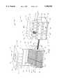
- FIG. 1is a perspective view of the chip sorting system of the invention, including a chip handler and a bin cart coupled thereto;
- FIG. 2is an enlarged perspective view of the portion of the side wall of the chip handler located within line 2 of FIG. 1;
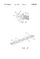
- FIG. 3is a perspective view of a plurality of chips housed within a chip packaging.
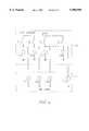
- FIG. 4is a circuit diagram illustrating one embodiment of an electrical interface used in the chip sorting system of FIG. 1.
- FIG. 1is a perspective view of a component or chip sorting system 40 of the invention.
- the chip sorting system 40includes a component or chip handler 42, which is a device that tests the quality of computer chips and then sorts the chips into groups according to their quality, as described more fully below.
- the chip sorting system 40further includes a bin cart 44 in which an operator places the groups of chips after they are sorted by the chip handler 42.
- the chip handler 42communicates with the bin cart 44 via a communication line or cable 46 to thereby assist the operator in correctly moving the groups of chips from the chip handler 42 to the bin cart 44, as described more fully below.
- a communication line or cable 46to thereby assist the operator in correctly moving the groups of chips from the chip handler 42 to the bin cart 44, as described more fully below.
- the chip handler 42comprises a main housing 48 having a front panel 50 positioned between a pair of side walls 64 and 66.
- the front panel 50includes any of a wide variety of control devices 51 for controlling and monitoring the operation of the chip handler 42.
- the control devices 51may comprise displays, keyboards, index switches, or any other of a wide variety of well-known control devices commonly used with chip handlers.
- a removable access panel 53is located on the top of the main housing 48 to provide access to an internal chamber (not shown) in which chips are inserted by a user and then processed by the chip handler 42. It will be appreciated that the chip handler 42 may take on any of a wide variety of shapes and sizes.
- the chip handler 42may comprise any of a wide variety of well known computer chip handling devices that sort and group computer chips according to the quality of the chip.
- the chip handlercomprises an MP3050 series BY8/16 Environmental Handler, manufactured by Symtek. It will be appreciated that the process by which the chip handler 42 tests and sorts chips 43 is well known to those skilled in the art.
- the main housing 48 of the chip handler 42surrounds a track area 49 located between the side walls 64 and 66 and below the front panel 50 of the chip handler 42.
- the track area 49includes several vertically-inclined tracks 54 that are aligned in rows adjacent one another.
- Each of the tracks 54has a top end 56 and a bottom end 58 and is sized to slidingly receive the computer chips 43.
- the tracks 54are sized to receive a series or column of chips 43.
- Each track 54is sized to hold a predetermined number of computer chips 43.
- the chip handler 42deposits the computer chips 60 onto the tracks 54 after the chip handler 42 tests the quality of the computer chips 60. Desirably, all of the chips 43 within a single track belong to a single group of chips 43, as described more fully below.
- a support bar 62extends over and across the track area 49 of the chip handler 42 between the side walls 64 and 66.
- a number of indicator lights 68are located on the support bar 62.
- the number of indicator lights 68is equal to the number of tracks 54 in the track area 49 so that each of the indicator lights 68 has an associated track 54.
- a track 54ahas an associated indicator light 68a located on the support bar 62 immediately above the track 54a. It will be appreciated that the indicator lights 68 may be located anywhere on the chip handler 42 as long as each track 54 has an associated indicator light 68.
- the bin cart 44is located adjacent the chip handler 42.
- the bin cart 44is substantially rectangular-shaped and includes a pair of opposed side walls 72 and 73.
- the bin cart 44also includes an upper platform 74 and a rear wall 75 connected thereto.
- the platform 74 and rear wall 75are also connected to the side walls 72 and 73, and are each oriented substantially normal to the side walls 72 and 73.
- Several additional platforms 79are located in a horizontal, stacked configuration below the platform 74.
- a number of intermediate walls 77are positioned between and parallel to the side walls 72 and 73, and are oriented vertically so as to extend between pairs of the horizontal platforms 74, 75 and parallel to the side walls 72 and 73, so that the intermediate walls 77 define a plurality of bin spaces 78 which are each sized to receive groups of computer chips 43, as described in more detail below.
- the number of bin spaces 78 in the bin cart 44is equal to the number of tracks 54 in the chip handler 42. Accordingly, each of the tracks 54 in the chip handler 42 has an associated bin space 78 in the bin cart 44.
- the bin cart 44also includes a set of wheels 55 to facilitate movement of the bin cart 44. It will be appreciated that the bin cart 44 may take on any of a wide variety of shapes and sizes and that the bin cart 44 may contain any of a wide number of bin spaces 78, although in the embodiment described herein, the number of bin spaces 78 is equal to the number of tracks 54 in the chip handler 42. Additionally, the size and shape of the bin spaces 78 may also be varied. The bin cart 44 may also be fixedly mounted on the ground adjacent the chip handler 42.
- each bin space 78has an associated indicator light 80 that is easily identifiable with its associated bin space 78.
- a bin space 78a on the bin cart 44has an associated indicator light 80a located immediately above the bin space 78a.
- each of the indicator lights 80 of the bin cart 44is arrow-shaped and points at its associated bin space 78. This assists a user in identifying which bin space 78 corresponds to which indicator light 80. It will be appreciated, however, that the indicator lights 80 may take on any of a wide variety of shapes and sizes.
- the communication cable 46extends between the chip handler 42 and the bin cart 44.
- the communication cable 46is elongated and includes a first end 86 and a second end 88.
- the first end 86 of the communication cable 46is coupled to the side wall 66 of the chip handler 42 near the location where the support bar 62 contacts the side wall 66.
- the second end 88 of the communication cable 46is coupled to the side wall 72 of the bin cart 44.
- the communication cable 46may have any of a wide variety of lengths. However, the communication cable 46 is desirably long enough to allow the chip handler 42 to be attached to the bin cart 44 via the communication cable 46 and yet still allow the bin cart 44 to be easily maneuvered on the wheels 55. In the embodiment shown in FIG. 1, the communication cable 46 is fixedly attached to the chip handler 42 and the bin cart 44. Alternatively, the communication cable 46 may be removably attached to the chip handler 42 and the bin cart 44, as described below with respect to FIG. 2.
- FIG. 2is an enlarged perspective view of the portion of the chip handler 42 within line 2 of FIG. 1.
- the first end 86 of the communication cable 46includes a coupling member 90 that is configured to mate with a coupling member 92 on the side wall 64 of the bin cart 44.
- the coupling member 90comprises at least one male prong 91.
- the coupling device 92 on the chip handler 42comprises a corresponding female receiving hole 93.
- the prong 91is sized and shaped to fit within the corresponding female receiving hole 93.
- the second end 88 (FIG. 1) of the communication cable 46 and the side wall 72 of the bin cart 44may also be equipped with a similar type of coupling configuration.
- the coupling members 90 and 92could comprise any of a wide variety of well known electrical coupling devices, such as, for example, a forty pin IDE connector, a two-prong electrical connection, a three-prong connection, etc.
- the communication cable 46could be fixedly mounted to the chip handler 42 and the bin cart 44.
- the communication cable 46provides a communication path between the chip handler 42 and the bin cart 44. That is, the communication cable 46 couples or links the indicator lights of 68 of the chip handler 42 to the indicator lights 80 of the bin cart 44. Desirably, when one of the indicator light 80 on the bin cart 44 is activated or illuminated, a corresponding indicator light 68 on the chip handler 42 is also illuminated, as described more fully below. In one embodiment, each of the indicator lights 68 of the chip handler 42 is hard-wired to a corresponding indicator light 80 on the bin cart 44 via the communication cable 46, as described more fully below.
- the indicator light 68a on the chip handler 42may be hard-wired to the indicator light 80a on the bin cart 44 so that the indicator light 80a automatically illuminates when the indicator light 68a illuminates. It is also contemplated that rather than direct wiring, a software program could be used to determined which of the indicator lights 68 on the chip handler 42 is illuminated. The software would then illuminate a corresponding indicator light 80 on the bin cart 44.
- the communication cable 46could also be replaced with a remote interface, such as an infrared signal device for communicating between the chip handler 42 and the bin cart 44.
- the chip sorting system 30may be used to test and sort computer chips according to certain criteria relating to the quality of the chip, such as, for example, the percentage of memory cells in the chip that are working correctly or the rated speed of a processor.
- An operatorfirst inserts a group of chips into the chip handler 42 via the removable access panel 53.
- the chip handler 42then tests the chips and determines a quality level of the chip. For example, certain chips may have 100% of their memory cells working properly and other chips may have 50% of their memory cells working properly or some processor may correctly operate at clock speeds higher than others.
- the chip handler 42sorts the chips into groups according to the quality of the chip.
- the chip handler 42sorts the chips into groups using the tracks 54 so that all of the chips within a single track 54 are chips of a common quality level.
- the process by which the chip handler 42 tests and sorts the chipsis well known to those skilled in the art.
- FIG. 1illustrates the track 54a as filled to capacity with chips 43.
- the corresponding indicator light 68ais illuminated, such as through a switch that is closed when a predetermined number of chips enter the track 68a. In this manner, the indicator light 68a notifies the person operating the chip handler 42 that the track 54a is filled to capacity.
- the other indicator lights on the chip handler 42also illuminate when their corresponding tracks have been filled to capacity.
- the package 94may comprise any of a wide variety of packaging materials for computer chips and that the package 94 may be configured to hold any of a wide number of computer chips.
- the package 94comprises an elongated tube of material, such as plastic, that is sized to receive a number of chips.
- the bottom end 58 of each of the tracks 54may be fitted with a release door that is opened to allow the chips to slide downward from the track 54 into the package 94.
- the operatormay simply lift the chips individually from the track 54.
- the operatortransfers the group of chips 43 to one of the bin spaces 78 on the bin cart 44.
- a corresponding indicator light 80 on the bin spaceis also illuminated.
- the communication cable 46provides a communication path between the indicator lights 68 on the chip handler 42 and the corresponding indicator lights 80 on the bin cart 44.
- the bin space 78 below the particular indicator light 80 that is illuminatedis the bin space that is used to store the chips from the track 54 that was filled to capacity.
- the indicator light 80continues to be lit after the operator removes the chips 43 from the chip handler 42, thereby notifying the operator as to which of the bin spaces 78 the chips are to be transferred into.
- the indicator light 68a on the chip handler 42is illuminated, indicating that the track 54a is filled to capacity.
- the corresponding indicator light 80a on the bin cartis also illuminated to notify the operator that the chips from the track 54a should be inserted into the associated bin space 78a. This greatly reduces the likelihood of the operator placing the chips into the wrong bin space 78 and mixing up the chips after they have been sorted by the chip handler 42.
- the indicator lights 80 on the bin cart 44may be illuminated in response to the operator removing chips from the track 54 or opening the release device on the track 54.
- the indicator lights 80 on the bin cart 44assist the user in properly removing the chips from the chip handler 42 and then inserting the chips into the proper bin space 78 in the bin cart 44.
- the indicator lights 68 and 80remain illuminated until the user depresses an acknowledgment switch that removes power to the illuminated lights 68 and 80.
- one embodiment of the electrical interface between the chip handler 42 and the bin cart 44is schematically illustrated in a circuit diagram.
- a plurality of controlled switches S 1 through S nconnect a voltage source 140 to each of the indicator lights L CH1 through L CHn , on the chip handler 42, where n is the number of indicator lights on the chip handler 42.
- the indicator lights L CH1 through L CHn on the chip handler 42are wired in parallel (via the communication cable 46) to corresponding indicator lights L BC1 through L BCn , respectively, on the bin cart 44.
- the switch S on the corresponding trackis closed.
- the corresponding indicator light L CHis then illuminated.
- the indicator light L BC on the bin cart 44is also energized and illuminated when the switch S closes.
- the useracknowledges transfer of the chips from the chip handler 42 to the bin cart 44 by manually opening the switch S, such as through a control button on the chip handler 42 or the bin cart 44. It will be appreciated that the illustrated circuit could also be varied or replaced with an encoder to signal between the chip handler 42 and the bin cart 44.
- the chip sorting system 40 of the present inventionthus advantageously assists an operator in properly packaging and arranging chips after they have been sorted by the chip handler 42.
- the coupling of the indicator lights 68 on the chip handler 42 to the indicator lights 80 on the bin cart 44reduces the likelihood of the operator improperly mixing the groups of chips after the chips are sorted by the chip handler 42.
Landscapes
- Physics & Mathematics (AREA)
- General Physics & Mathematics (AREA)
- Testing Of Individual Semiconductor Devices (AREA)
Abstract
Description
Claims (22)
Priority Applications (1)
| Application Number | Priority Date | Filing Date | Title |
|---|---|---|---|
| US09/027,131US5996996A (en) | 1998-02-20 | 1998-02-20 | Method of sorting computer chips |
Applications Claiming Priority (1)
| Application Number | Priority Date | Filing Date | Title |
|---|---|---|---|
| US09/027,131US5996996A (en) | 1998-02-20 | 1998-02-20 | Method of sorting computer chips |
Publications (1)
| Publication Number | Publication Date |
|---|---|
| US5996996Atrue US5996996A (en) | 1999-12-07 |
Family
ID=21835871
Family Applications (1)
| Application Number | Title | Priority Date | Filing Date |
|---|---|---|---|
| US09/027,131Expired - LifetimeUS5996996A (en) | 1998-02-20 | 1998-02-20 | Method of sorting computer chips |
Country Status (1)
| Country | Link |
|---|---|
| US (1) | US5996996A (en) |
Cited By (22)
| Publication number | Priority date | Publication date | Assignee | Title |
|---|---|---|---|---|
| US6124559A (en)* | 1997-12-17 | 2000-09-26 | Advanced Micro Devices, Inc. | Integrated circuit sorter that automatically prevents binning of integrated circuits into a wrong container |
| US6563070B2 (en) | 1999-03-30 | 2003-05-13 | Micron Technology, Inc. | Enhanced grading and sorting of semiconductor devices using modular “plug-in” sort algorithms |
| US6781363B2 (en)* | 2001-06-21 | 2004-08-24 | Han-Ping Chen | Memory sorting method and apparatus |
| US20040267854A1 (en)* | 2003-06-26 | 2004-12-30 | Towfique Haider | Logarithmic and inverse logarithmic conversion system and method |
| US20050099711A1 (en)* | 2003-11-10 | 2005-05-12 | Honda Motor Co., Ltd. | Magnesium mirror base with countermeasures for galvanic corrosion |
| US20050251761A1 (en)* | 2003-09-15 | 2005-11-10 | Diamond Michael B | Integrated circuit configuration system and method |
| US20070162624A1 (en)* | 2005-12-12 | 2007-07-12 | Tamasi Anthony M | System and method for configurable digital communication |
| US20070246880A1 (en)* | 2006-04-19 | 2007-10-25 | Kenji Totsuka | Methods For Moving A Media Sheet Within An Image Forming Device |
| US20080106328A1 (en)* | 2004-09-15 | 2008-05-08 | Diamond Michael B | Semiconductor die micro electro-mechanical switch management system and method |
| US20080174595A1 (en)* | 2005-04-25 | 2008-07-24 | Jatou Ross F | Controlled impedance display adapter |
| US20090103443A1 (en)* | 2007-10-22 | 2009-04-23 | Ting Sheng Ku | Loopback configuration for bi-directional interfaces |
| US7793029B1 (en) | 2005-05-17 | 2010-09-07 | Nvidia Corporation | Translation device apparatus for configuring printed circuit board connectors |
| US20100309918A1 (en)* | 2009-06-04 | 2010-12-09 | Nvidia Corporation | Method and system for ordering posted packets and non-posted packets transfer |
| US20110216780A1 (en)* | 2010-03-04 | 2011-09-08 | Nvidia Corporation | Input/Output Request Packet Handling Techniques by a Device Specific Kernel Mode Driver |
| US8412872B1 (en) | 2005-12-12 | 2013-04-02 | Nvidia Corporation | Configurable GPU and method for graphics processing using a configurable GPU |
| US8711156B1 (en) | 2004-09-30 | 2014-04-29 | Nvidia Corporation | Method and system for remapping processing elements in a pipeline of a graphics processing unit |
| US8711161B1 (en) | 2003-12-18 | 2014-04-29 | Nvidia Corporation | Functional component compensation reconfiguration system and method |
| US8732644B1 (en) | 2003-09-15 | 2014-05-20 | Nvidia Corporation | Micro electro mechanical switch system and method for testing and configuring semiconductor functional circuits |
| US8775997B2 (en) | 2003-09-15 | 2014-07-08 | Nvidia Corporation | System and method for testing and configuring semiconductor functional circuits |
| US9092170B1 (en) | 2005-10-18 | 2015-07-28 | Nvidia Corporation | Method and system for implementing fragment operation processing across a graphics bus interconnect |
| US9176909B2 (en) | 2009-12-11 | 2015-11-03 | Nvidia Corporation | Aggregating unoccupied PCI-e links to provide greater bandwidth |
| US9330031B2 (en) | 2011-12-09 | 2016-05-03 | Nvidia Corporation | System and method for calibration of serial links using a serial-to-parallel loopback |
Citations (17)
| Publication number | Priority date | Publication date | Assignee | Title |
|---|---|---|---|---|
| US2902152A (en)* | 1957-07-15 | 1959-09-01 | Wilkes Reuben | Drill calibrator and sorter |
| US3716786A (en)* | 1970-10-02 | 1973-02-13 | Cogar Corp | Module tester and sorter for use in a module test system |
| US3980553A (en)* | 1975-05-09 | 1976-09-14 | Lorlin Industries Inc. | Automatic feeding and sorting equipment for electrical components |
| US4168004A (en)* | 1978-03-06 | 1979-09-18 | Owen Tri-Cut Limited | Mail processing equipment |
| US4388994A (en)* | 1979-11-14 | 1983-06-21 | Nippon Electric Co., Ltd. | Flat-article sorting apparatus |
| US4478352A (en)* | 1982-05-19 | 1984-10-23 | Micro Component Technology, Inc. | Integrated circuit component handler singulation apparatus |
| US4588092A (en)* | 1983-11-15 | 1986-05-13 | Automated Electronic Technology, Inc. | Integrated circuit handling and contact system |
| US4694964A (en)* | 1983-11-07 | 1987-09-22 | Ekkehard Ueberreiter | Device for conveying components particularly integrated chips, from an input magazine to an output magazine |
| US4826019A (en)* | 1983-12-23 | 1989-05-02 | Three Phoenix Company | Handling apparatus for magnetic recording disks |
| US4836916A (en)* | 1983-12-23 | 1989-06-06 | Three Phoenix Company | Handling apparatus for magnetic recording disks |
| US4871963A (en)* | 1986-07-22 | 1989-10-03 | Sgs Microelettronica S.P.A. | Method and apparatus for testing EPROM type semiconductor devices during burn-in |
| US5465850A (en)* | 1992-03-11 | 1995-11-14 | Nec Corporation | Integrated circuit test system |
| US5470427A (en)* | 1991-01-16 | 1995-11-28 | Pitney Bowes Inc. | Postal automated labeling system |
| US5538141A (en)* | 1994-09-27 | 1996-07-23 | Intel Corporation | Test flow assurance using memory imprinting |
| US5568870A (en)* | 1994-08-18 | 1996-10-29 | Testec, Inc. | Device for testing and sorting small electronic components |
| US5584395A (en)* | 1994-03-24 | 1996-12-17 | Nec Corporation | High speed sorting apparatus for semiconductor device equipped with rotatable sorting drum |
| US5794789A (en)* | 1995-12-13 | 1998-08-18 | Payson; William H. | Semi-automated integrated sort system |
- 1998
- 1998-02-20USUS09/027,131patent/US5996996A/ennot_activeExpired - Lifetime
Patent Citations (19)
| Publication number | Priority date | Publication date | Assignee | Title |
|---|---|---|---|---|
| US2902152A (en)* | 1957-07-15 | 1959-09-01 | Wilkes Reuben | Drill calibrator and sorter |
| US3716786A (en)* | 1970-10-02 | 1973-02-13 | Cogar Corp | Module tester and sorter for use in a module test system |
| US3980553A (en)* | 1975-05-09 | 1976-09-14 | Lorlin Industries Inc. | Automatic feeding and sorting equipment for electrical components |
| US4168004A (en)* | 1978-03-06 | 1979-09-18 | Owen Tri-Cut Limited | Mail processing equipment |
| US4388994A (en)* | 1979-11-14 | 1983-06-21 | Nippon Electric Co., Ltd. | Flat-article sorting apparatus |
| US4478352A (en)* | 1982-05-19 | 1984-10-23 | Micro Component Technology, Inc. | Integrated circuit component handler singulation apparatus |
| US4694964A (en)* | 1983-11-07 | 1987-09-22 | Ekkehard Ueberreiter | Device for conveying components particularly integrated chips, from an input magazine to an output magazine |
| US4588092A (en)* | 1983-11-15 | 1986-05-13 | Automated Electronic Technology, Inc. | Integrated circuit handling and contact system |
| US4826019A (en)* | 1983-12-23 | 1989-05-02 | Three Phoenix Company | Handling apparatus for magnetic recording disks |
| US4836916A (en)* | 1983-12-23 | 1989-06-06 | Three Phoenix Company | Handling apparatus for magnetic recording disks |
| US4871963A (en)* | 1986-07-22 | 1989-10-03 | Sgs Microelettronica S.P.A. | Method and apparatus for testing EPROM type semiconductor devices during burn-in |
| US5470427A (en)* | 1991-01-16 | 1995-11-28 | Pitney Bowes Inc. | Postal automated labeling system |
| US5465850A (en)* | 1992-03-11 | 1995-11-14 | Nec Corporation | Integrated circuit test system |
| US5584395A (en)* | 1994-03-24 | 1996-12-17 | Nec Corporation | High speed sorting apparatus for semiconductor device equipped with rotatable sorting drum |
| US5568870A (en)* | 1994-08-18 | 1996-10-29 | Testec, Inc. | Device for testing and sorting small electronic components |
| US5538141A (en)* | 1994-09-27 | 1996-07-23 | Intel Corporation | Test flow assurance using memory imprinting |
| US5603412A (en)* | 1994-09-27 | 1997-02-18 | Intel Corporation | Apparatus and semiconductor component for assuring test flow compliance |
| US5895443A (en)* | 1994-09-27 | 1999-04-20 | Intel Corporation | Testable non-volatile memory device |
| US5794789A (en)* | 1995-12-13 | 1998-08-18 | Payson; William H. | Semi-automated integrated sort system |
Cited By (38)
| Publication number | Priority date | Publication date | Assignee | Title |
|---|---|---|---|---|
| US6124559A (en)* | 1997-12-17 | 2000-09-26 | Advanced Micro Devices, Inc. | Integrated circuit sorter that automatically prevents binning of integrated circuits into a wrong container |
| US6563070B2 (en) | 1999-03-30 | 2003-05-13 | Micron Technology, Inc. | Enhanced grading and sorting of semiconductor devices using modular “plug-in” sort algorithms |
| US6633014B2 (en) | 1999-03-30 | 2003-10-14 | Micron Technology, Inc. | Enhanced grading and sorting of semiconductor devices using modular “plug-in” sort algorithms |
| US6747228B2 (en) | 1999-03-30 | 2004-06-08 | Micron Technology, Inc. | Enhanced grading and sorting of semiconductor devices using modular “plug-in” sort algorithms |
| US6781363B2 (en)* | 2001-06-21 | 2004-08-24 | Han-Ping Chen | Memory sorting method and apparatus |
| US20040267854A1 (en)* | 2003-06-26 | 2004-12-30 | Towfique Haider | Logarithmic and inverse logarithmic conversion system and method |
| US8872833B2 (en) | 2003-09-15 | 2014-10-28 | Nvidia Corporation | Integrated circuit configuration system and method |
| US8732644B1 (en) | 2003-09-15 | 2014-05-20 | Nvidia Corporation | Micro electro mechanical switch system and method for testing and configuring semiconductor functional circuits |
| US20050251358A1 (en)* | 2003-09-15 | 2005-11-10 | Van Dyke James M | System and method for increasing die yield |
| US20060004536A1 (en)* | 2003-09-15 | 2006-01-05 | Diamond Michael B | System and method for remotely configuring semiconductor functional circuits |
| US20050251761A1 (en)* | 2003-09-15 | 2005-11-10 | Diamond Michael B | Integrated circuit configuration system and method |
| US8788996B2 (en)* | 2003-09-15 | 2014-07-22 | Nvidia Corporation | System and method for configuring semiconductor functional circuits |
| US8768642B2 (en) | 2003-09-15 | 2014-07-01 | Nvidia Corporation | System and method for remotely configuring semiconductor functional circuits |
| US8775112B2 (en)* | 2003-09-15 | 2014-07-08 | Nvidia Corporation | System and method for increasing die yield |
| US8775997B2 (en) | 2003-09-15 | 2014-07-08 | Nvidia Corporation | System and method for testing and configuring semiconductor functional circuits |
| US20050099711A1 (en)* | 2003-11-10 | 2005-05-12 | Honda Motor Co., Ltd. | Magnesium mirror base with countermeasures for galvanic corrosion |
| US8711161B1 (en) | 2003-12-18 | 2014-04-29 | Nvidia Corporation | Functional component compensation reconfiguration system and method |
| US20080106328A1 (en)* | 2004-09-15 | 2008-05-08 | Diamond Michael B | Semiconductor die micro electro-mechanical switch management system and method |
| US8704275B2 (en) | 2004-09-15 | 2014-04-22 | Nvidia Corporation | Semiconductor die micro electro-mechanical switch management method |
| US8723231B1 (en) | 2004-09-15 | 2014-05-13 | Nvidia Corporation | Semiconductor die micro electro-mechanical switch management system and method |
| US8711156B1 (en) | 2004-09-30 | 2014-04-29 | Nvidia Corporation | Method and system for remapping processing elements in a pipeline of a graphics processing unit |
| US8021193B1 (en) | 2005-04-25 | 2011-09-20 | Nvidia Corporation | Controlled impedance display adapter |
| US20080174595A1 (en)* | 2005-04-25 | 2008-07-24 | Jatou Ross F | Controlled impedance display adapter |
| US8021194B2 (en) | 2005-04-25 | 2011-09-20 | Nvidia Corporation | Controlled impedance display adapter |
| US7793029B1 (en) | 2005-05-17 | 2010-09-07 | Nvidia Corporation | Translation device apparatus for configuring printed circuit board connectors |
| US9092170B1 (en) | 2005-10-18 | 2015-07-28 | Nvidia Corporation | Method and system for implementing fragment operation processing across a graphics bus interconnect |
| US8417838B2 (en) | 2005-12-12 | 2013-04-09 | Nvidia Corporation | System and method for configurable digital communication |
| US8412872B1 (en) | 2005-12-12 | 2013-04-02 | Nvidia Corporation | Configurable GPU and method for graphics processing using a configurable GPU |
| US20070162624A1 (en)* | 2005-12-12 | 2007-07-12 | Tamasi Anthony M | System and method for configurable digital communication |
| US20070246880A1 (en)* | 2006-04-19 | 2007-10-25 | Kenji Totsuka | Methods For Moving A Media Sheet Within An Image Forming Device |
| US20090103443A1 (en)* | 2007-10-22 | 2009-04-23 | Ting Sheng Ku | Loopback configuration for bi-directional interfaces |
| US8724483B2 (en) | 2007-10-22 | 2014-05-13 | Nvidia Corporation | Loopback configuration for bi-directional interfaces |
| US8687639B2 (en) | 2009-06-04 | 2014-04-01 | Nvidia Corporation | Method and system for ordering posted packets and non-posted packets transfer |
| US20100309918A1 (en)* | 2009-06-04 | 2010-12-09 | Nvidia Corporation | Method and system for ordering posted packets and non-posted packets transfer |
| US9176909B2 (en) | 2009-12-11 | 2015-11-03 | Nvidia Corporation | Aggregating unoccupied PCI-e links to provide greater bandwidth |
| US20110216780A1 (en)* | 2010-03-04 | 2011-09-08 | Nvidia Corporation | Input/Output Request Packet Handling Techniques by a Device Specific Kernel Mode Driver |
| US9331869B2 (en) | 2010-03-04 | 2016-05-03 | Nvidia Corporation | Input/output request packet handling techniques by a device specific kernel mode driver |
| US9330031B2 (en) | 2011-12-09 | 2016-05-03 | Nvidia Corporation | System and method for calibration of serial links using a serial-to-parallel loopback |
Similar Documents
| Publication | Publication Date | Title |
|---|---|---|
| US5996996A (en) | Method of sorting computer chips | |
| US5998751A (en) | Sorting system for computer chips | |
| DE19680785B4 (en) | A semiconductor device test apparatus and semiconductor device test system including a plurality of semiconductor device test equipment | |
| US4940935A (en) | Automatic SMD tester | |
| KR100270137B1 (en) | Container for ic tyays and base plate for mounting the container | |
| JP2769026B2 (en) | Sample sorting device | |
| US5788084A (en) | Automatic testing system and method for semiconductor devices | |
| US6563331B1 (en) | Test and burn-in apparatus, in-line system using the test and burn-in apparatus, and test method using the in-line system | |
| US5150797A (en) | IC sorting and receiving apparatus and method | |
| CN102323564A (en) | Electric energy meter verification unit and its working method | |
| US5909657A (en) | Semiconductor device testing apparatus | |
| WO1997005495A1 (en) | Semiconductor device tester | |
| JPH0643212A (en) | Automatic test handler | |
| CN107533102A (en) | Element processor | |
| KR100401014B1 (en) | Test Handler | |
| JP3134738B2 (en) | Handling system | |
| MY113318A (en) | Device transfer and reinspection method for ic handler | |
| CN112824850B (en) | A get and put material controlling means and module check out test set for can opening and shutting frock | |
| CN208495010U (en) | Solid state hard disk test macro loading and unloading all-in-one machine | |
| JP3246308B2 (en) | IC device transfer device | |
| KR100295703B1 (en) | Semiconductor device testing apparatus and semiconductor device testing system having a plurality of semiconductor device testing apparatus | |
| CN212722960U (en) | Automatic separating mechanism and testing device | |
| US7902477B1 (en) | Integrated circuit test work station | |
| KR100260121B1 (en) | Autohandler with stocker for screening | |
| CN214718565U (en) | Fool-proof device for semiconductor test |
Legal Events
| Date | Code | Title | Description |
|---|---|---|---|
| AS | Assignment | Owner name:MICRON ELECTRONICS, INC., IDAHO Free format text:ASSIGNMENT OF ASSIGNORS INTEREST;ASSIGNOR:BRUNELLE, STEVE;REEL/FRAME:009260/0305 Effective date:19980603 | |
| STCF | Information on status: patent grant | Free format text:PATENTED CASE | |
| AS | Assignment | Owner name:MEI CALIFORNIA, INC., CALIFORNIA Free format text:ASSIGNMENT OF ASSIGNORS INTEREST;ASSIGNOR:MICRON ELECTRONICS, INC.;REEL/FRAME:011658/0956 Effective date:20010322 | |
| AS | Assignment | Owner name:MICRON TECHNOLOGY, INC., IDAHO Free format text:ASSIGNMENT OF ASSIGNORS INTEREST;ASSIGNOR:MEI CALIFORNIA INC;REEL/FRAME:012232/0436 Effective date:20010322 | |
| FEPP | Fee payment procedure | Free format text:PAYOR NUMBER ASSIGNED (ORIGINAL EVENT CODE: ASPN); ENTITY STATUS OF PATENT OWNER: LARGE ENTITY | |
| FPAY | Fee payment | Year of fee payment:4 | |
| FEPP | Fee payment procedure | Free format text:PAYOR NUMBER ASSIGNED (ORIGINAL EVENT CODE: ASPN); ENTITY STATUS OF PATENT OWNER: LARGE ENTITY Free format text:PAYER NUMBER DE-ASSIGNED (ORIGINAL EVENT CODE: RMPN); ENTITY STATUS OF PATENT OWNER: LARGE ENTITY | |
| FPAY | Fee payment | Year of fee payment:8 | |
| FEPP | Fee payment procedure | Free format text:PAYOR NUMBER ASSIGNED (ORIGINAL EVENT CODE: ASPN); ENTITY STATUS OF PATENT OWNER: LARGE ENTITY Free format text:PAYER NUMBER DE-ASSIGNED (ORIGINAL EVENT CODE: RMPN); ENTITY STATUS OF PATENT OWNER: LARGE ENTITY | |
| FPAY | Fee payment | Year of fee payment:12 | |
| AS | Assignment | Owner name:U.S. BANK NATIONAL ASSOCIATION, AS COLLATERAL AGENT, CALIFORNIA Free format text:SECURITY INTEREST;ASSIGNOR:MICRON TECHNOLOGY, INC.;REEL/FRAME:038669/0001 Effective date:20160426 Owner name:U.S. BANK NATIONAL ASSOCIATION, AS COLLATERAL AGEN Free format text:SECURITY INTEREST;ASSIGNOR:MICRON TECHNOLOGY, INC.;REEL/FRAME:038669/0001 Effective date:20160426 | |
| AS | Assignment | Owner name:MORGAN STANLEY SENIOR FUNDING, INC., AS COLLATERAL AGENT, MARYLAND Free format text:PATENT SECURITY AGREEMENT;ASSIGNOR:MICRON TECHNOLOGY, INC.;REEL/FRAME:038954/0001 Effective date:20160426 Owner name:MORGAN STANLEY SENIOR FUNDING, INC., AS COLLATERAL Free format text:PATENT SECURITY AGREEMENT;ASSIGNOR:MICRON TECHNOLOGY, INC.;REEL/FRAME:038954/0001 Effective date:20160426 | |
| AS | Assignment | Owner name:U.S. BANK NATIONAL ASSOCIATION, AS COLLATERAL AGENT, CALIFORNIA Free format text:CORRECTIVE ASSIGNMENT TO CORRECT THE REPLACE ERRONEOUSLY FILED PATENT #7358718 WITH THE CORRECT PATENT #7358178 PREVIOUSLY RECORDED ON REEL 038669 FRAME 0001. ASSIGNOR(S) HEREBY CONFIRMS THE SECURITY INTEREST;ASSIGNOR:MICRON TECHNOLOGY, INC.;REEL/FRAME:043079/0001 Effective date:20160426 Owner name:U.S. BANK NATIONAL ASSOCIATION, AS COLLATERAL AGEN Free format text:CORRECTIVE ASSIGNMENT TO CORRECT THE REPLACE ERRONEOUSLY FILED PATENT #7358718 WITH THE CORRECT PATENT #7358178 PREVIOUSLY RECORDED ON REEL 038669 FRAME 0001. ASSIGNOR(S) HEREBY CONFIRMS THE SECURITY INTEREST;ASSIGNOR:MICRON TECHNOLOGY, INC.;REEL/FRAME:043079/0001 Effective date:20160426 | |
| AS | Assignment | Owner name:MICRON TECHNOLOGY, INC., IDAHO Free format text:RELEASE BY SECURED PARTY;ASSIGNOR:U.S. BANK NATIONAL ASSOCIATION, AS COLLATERAL AGENT;REEL/FRAME:047243/0001 Effective date:20180629 | |
| AS | Assignment | Owner name:MICRON TECHNOLOGY, INC., IDAHO Free format text:RELEASE BY SECURED PARTY;ASSIGNOR:MORGAN STANLEY SENIOR FUNDING, INC., AS COLLATERAL AGENT;REEL/FRAME:050937/0001 Effective date:20190731 |