US5994732A - Nonvolatile semiconductor memory device - Google Patents
Nonvolatile semiconductor memory deviceDownload PDFInfo
- Publication number
- US5994732A US5994732AUS08/852,817US85281797AUS5994732AUS 5994732 AUS5994732 AUS 5994732AUS 85281797 AUS85281797 AUS 85281797AUS 5994732 AUS5994732 AUS 5994732A
- Authority
- US
- United States
- Prior art keywords
- well
- memory
- memory transistor
- region
- erase
- Prior art date
- Legal status (The legal status is an assumption and is not a legal conclusion. Google has not performed a legal analysis and makes no representation as to the accuracy of the status listed.)
- Expired - Lifetime
Links
Images


Classifications
- H—ELECTRICITY
- H10—SEMICONDUCTOR DEVICES; ELECTRIC SOLID-STATE DEVICES NOT OTHERWISE PROVIDED FOR
- H10B—ELECTRONIC MEMORY DEVICES
- H10B69/00—Erasable-and-programmable ROM [EPROM] devices not provided for in groups H10B41/00 - H10B63/00, e.g. ultraviolet erasable-and-programmable ROM [UVEPROM] devices
- G—PHYSICS
- G11—INFORMATION STORAGE
- G11C—STATIC STORES
- G11C16/00—Erasable programmable read-only memories
- G11C16/02—Erasable programmable read-only memories electrically programmable
- G11C16/06—Auxiliary circuits, e.g. for writing into memory
- G11C16/10—Programming or data input circuits
- G11C16/14—Circuits for erasing electrically, e.g. erase voltage switching circuits
- G11C16/16—Circuits for erasing electrically, e.g. erase voltage switching circuits for erasing blocks, e.g. arrays, words, groups
Definitions
- the present inventionrelates to a nonvolatile semiconductor memory device and more particularly to an electrically programmable and erasable nonvolatile semiconductor memory device (hereinafter referred to as a "flash memory”) including stacked gate type memory cells (memory transistors).
- flash memoryelectrically programmable and erasable nonvolatile semiconductor memory device
- memory transistorsstacked gate type memory cells
- FIG. 5shows a cross sectional structure of a general stacked gate type memory transistor 11 formed within a conventional flash memory.
- drain and source regions 4 and 5are formed spaced apart at a surface of a p well region 3.
- the drain and source regions 4 and 5in this case include an n type impurity of high concentration.
- a floating gate 8is formed on this tunnel insulating film 7, and a control gate (word line) 10 is formed on this floating gate 8 with an interlayer insulating film 9 therebetween.
- memory transistor 11has a double gate structure.
- the above-described p well region 3may be replaced by a p type semiconductor substrate.
- Memory transistor 11 having the above structureis kept in an erased state or a programmed state.
- Erasingcollectively changes threshold voltages of a plurality of memory transistors 11 to one prescribed state, while programming changes a threshold voltage of a selected memory transistor 11 to another prescribed state.
- the above erasing or programmingis performed depending on whether electrons are accumulated in floating gate 8 shown in FIG. 5 or emitted from floating gate 8.
- the one called a DINOR (DIvided bit-line NOR) type flash memoryis disclosed in IEICE TRANS. ELECTRON., VOL. E77-C, NO.8 AUGUST 1994, PP.1279 ⁇ 1286.
- the above-described DINOR type flash memoryis in the erased state when electrons are accumulated in floating gate 8 and it is in the programmed state when electrons are drawn out of floating gate 8.
- FIG. 6shows the erased and programmed states of memory transistor 11 in the DINOR type flash memory.
- threshold voltage of memory transistor 11becomes relatively high. Therefore, current (sense current) of not less than a given value will not flow between drain 4 and source 5 if control gate voltage does not exceed Vg1 as shown in FIG. 6. This is because positive voltage is canceled by a negative charge of electrons accumulated in floating gate 8.
- Such an erased statecorresponds to "1" in FIG. 6. Since electrons accumulated in floating gate 8 do not disappear almost permanently if left as they are, data stored in the gate will also be retained almost forever.
- drain 4is supplied with a write voltage (positive high voltage) Vw (approximately 6 V in general), control gate 10 is supplied with a negative high voltage -Vpp (approximately -10 v), and source 5 is kept open. Therefore, electrons are drawn out of floating gate 8 into drain 4 through an overlapped region of drain 4 and floating gate 8 because of the FN tunnel phenomenon. As a result, the threshold voltage of memory transistor 11 is lowered.
- Vwpositive high voltage
- Vppapproximately -10 v
- drain 4is kept in a floating state
- source 5 and p well region 3are supplied with the negative high voltage -Vpp
- control gate 10is supplied with a positive high voltage +Vpp. Therefore, a high electric field is applied to a tunnel insulating film 7, and electrons are injected into floating gate 8 from p well region 3 (semiconductor substrate) due to the tunnel phenomenon. As a result, the threshold voltage of memory transistor 11 is raised.
- memory transistor 11By supplying the above-described voltages to memory transistor 11, memory transistor 11 is shifted to the erased or programmed state and data is programmed or erased.
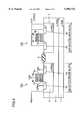
- the erase operation of the DINOR type flash memoryis accompanied by such problems as described below. The problems will be described with respect to FIGS. 8 and 9.
- FIG. 8is a block diagram showing circuits related to the erase operation of a conventional DINOR type flash memory.
- a well driver 60supplies a prescribed voltage to p well region 3a
- well decoder 71selects a prescribed p well region 3a
- well power supply 50generates a prescribed voltage which is supplied to p well region 3a.
- a plurality of erase blocks 26are arranged within a p well region 3a.
- a plurality of memory transistors 11constitute these erase blocks 26 for each of which collective erasing is performed.
- a source line(not shown) connected to sources 5 of memory transistors 11 in each erase block 26 is formed, and it is connected to a source line driver 61.
- Source line driver 61supplies a prescribed voltage to the source line and it is connected to a block decoder 70 and a source power supply 51.
- Block decoder 70is provided corresponding to each p well region 3a and it selects a prescribed erase block 26 in each p well region 3a.
- Source power supply 51generates a prescribed voltage which is applied to the source line.
- FIG. 9is an illustration showing the erase operation of the conventional flash memory.
- erase block 26which is selected (selected erase block) coexists with erase block 26 which is not selected (non-selected erase block) on the same p well region 3a as shown in FIG. 9.
- -Vppis supplied to p well region 3a.
- a control gate 10a of a memory transistor 11a within the selected erase blockis supplied with +Vpp, its drain 4a is set to an open state, and its source 5a is supplied with -Vpp.
- a control gate of a memory transistor 11b within the non-selected erase blockis grounded, its drain 4b is set to the open state, and its source 5b is supplied with -1/2Vpp as an erase inhibiting voltage.
- memory transistor 11b in the non-selected erase block and memory transistor 11a in the selected erase blockare formed on the same p well region 3a, the emission of electrons from floating gate 8b can not be inhibited perfectly even if the erase inhibiting voltage -1/2Vpp is supplied to source 5b of memory transistor 11b in the non-selected erase block. In other words, a small amount of electrons is drawn out of floating gate 8b.
- some erase blocks 26may be falsely erased when a large number of erase blocks are arranged within the same p well region 3a or when data is rewritten many times. Such phenomenon is referred to as a well disturbance in this specification. This well disturbance becomes more serious as flash memories come to have larger storage capacity.
- the present inventionis directed for solving the above problems and its object is to provide a nonvolatile semiconductor memory device which can prevent the generation of the well disturbance in the erase operation.
- the nonvolatile semiconductor memory device in accordance with the present inventionhas a plurality of memory transistors formed on a memory cell array region at a main surface of a semiconductor substrate and each including a floating gate, a source and a drain, its erase operation is performed when electrons are injected into the floating gate from the semiconductor substrate and its program operation is performed when electrons are drawn out of the floating gate to the semiconductor substrate.
- the nonvolatile semiconductor memory device in accordance with the inventionincludes first and second well regions, first and second erase blocks, and a common voltage supplying circuit.
- the first and second well regionsare formed spaced apart in the memory cell array region.
- the first erase blockincludes a first memory transistor group formed on the first well region.
- the second erase blockincludes a second memory transistor group formed on the second well region.
- the voltage supplying circuitis connected to the first and second well regions, and connected to sources of the first and second memory transistor groups with a switching circuit therebetween, in order to supply a prescribed voltage to the first and second well regions and to sources of the first
- the nonvolatile semiconductor memory device in accordance with the inventionhas an independent well formed for each erase block, each well being connected to the common voltage supplying circuit. Therefore, in the erase operation, different voltages can be supplied to a well arranged in a selected erase block and to a well arranged in a non-selected erase block, respectively. It can effectively prevent the occurrence of the well disturbance in a memory transistor of the non-selected erase block when the erase operation is performed.
- the voltage supplying circuitincludes a common well/source driver connected to the first and second well regions and to sources of the first and second memory transistor groups, a well/block decoder connected to this well/source driver for selecting the first or second well region and the first or second erase block, and a common well/source power supply connected to the well/source driver.
- the voltage supplying circuitis structured as above, its circuit structure can be made simpler than the prior art. The reasons will be described below. Since the independent well is formed for each erase block as described above, there is no need to supply the erase inhibiting voltage (-1/2Vpp) to a source of a memory transistor in a non-selected erase block. That makes it possible to replace, for example, a source power supply 51 shown in FIG. 8 with a well power supply 50. As a result, source power supply 51 can be omitted. Since one erase block is arranged for each well region, a well decoder 71, for example, shown in FIG. 8 can be replaced by a block decoder 70. That makes it possible to omit well decoder 71 shown in FIG. 8.
- well driver 71 shown in FIG. 8can be replaced by a source line driver 61.
- source line driver 61 shown in FIG. 8can be omitted.
- the nonvolatile semiconductor memory devicecan be simplified in its circuit structure as compared with the prior art and it can also be controlled easily because it does not require the erase inhibiting voltage.
- a third well regionis formed in the memory cell array region, and a redundancy block having the same structure as the first or second erase block for repairing a defect, if any, is formed on the third well region.
- the redundancy blockhas the same structure as the erase block as described above, the well disturbance can be effectively inhibited in the redundancy block. As a result, the erase block can be replaced by the redundancy block without the well disturbance.
- first and second select gate transistorsare respectively formed on the first and second well regions
- first and second sub bit linesare respectively formed on the first and second memory transistor groups with an insulating layer therebetween, connected to drains of a plurality of memory transistors in the first and second memory transistor groups
- a main bit lineis formed on the first and second sub bit lines with an insulating layer therebetween.
- the main bit lineis connected to the first sub bit line via the first select gate transistor and to the second sub bit line via the second select gate transistor.
- the first and second select gate transistorsare respectively formed as described above, the first and second select gate transistors can control connection/disconnection of the main bit line to/from the first and second sub bit lines. That effectively inhibits a drain disturbance in each erase block when the erase operation is performed.
- an isolating regionis formed surrounding the first and second well regions to isolate between the first and second well regions as well as to isolate the first and second well regions from other regions.
- respective first and second source linesare preferably formed with an insulating layer therebetween, electrically connected to sources of the first and second memory transistor groups.
- an auxiliary source line for lowering resistance of the first or second source lineis preferably formed, connected to the first or second source line.
- the auxiliary source linecan be formed on this isolating region.
- This auxiliary source lineis connected to the first or second source line. Provision of such auxiliary source line can lower the source line resistance.
- a plurality of memory transistors in the first memory transistor groupshare a first word line formed on floating gates of this plurality of memory transistors with the insulating layer therebetween and that the first erase block is arranged along the entire length of the first word line to include all memory transistors sharing the first word line. It is also preferred that a plurality of memory transistors in the second memory transistor group share a second word line formed on floating gates of this plurality of memory transistors with the insulating layers therebetween and that the second erase block is arranged along the entire length of the second word line to include all memory transistors sharing the second word line.
- the first or second erase blockis arranged along the entire length of the first or second word line as described above, all memory transistors sharing the first or second word line can be included in the first or second erase block. Therefore, it can be effectively inhibited to cause the disturbance in other erase blocks by the first or second word line when the erase operation is performed.
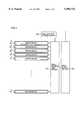
- FIG. 1is a block diagram showing circuits related to the erase operation of a DINOR type flash memory in accordance with one embodiment of the present invention.
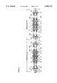
- FIG. 2is a partial plan view of the DINOR type flash memory in accordance with the embodiment of the present invention.
- FIG. 3is a cross sectional view taken along a line III--III of FIG. 2.
- FIG. 4is a schematic view showing the erase operation of the DINOR type flash memory in accordance with the present invention.
- FIG. 5is a cross sectional view showing one memory transistor in a conventional flash memory.
- FIG. 6is a graph showing the erased state and the programmed state of the conventional DINOR type flash memory.
- FIG. 7Ais a schematic view showing the program operation of the conventional DINOR type flash memory.
- FIG. 7Bis a schematic view showing the erase operation of the conventional DINOR type flash memory.
- FIG. 8is a block diagram showing circuits related to the erased state of the conventional DINOR type flash memory.
- FIG. 9is a schematic view showing the erase operation of the conventional flash memory.
- FIG. 1is a block diagram showing circuits related to the erase operation of a DINOR type flash memory in one embodiment of the present invention.
- a plurality of p well regions 3are formed spaced apart in a memory cell array region of a flash memory.
- One erase block 26is arranged in each p well region 3.
- P well regions 3are electrically isolated one another. Since each erase block 26 is arranged in p well region 3 which is isolated from other p well regions 3 as described above, a well disturbance in the erase operation can be effectively inhibited.
- Each p well region 3is connected to a well/source line driver 60a.
- a source line connected to sources of a plurality of memory transistors arranged in each erase block 26is connected to well/source line driver 60a via a switching element. Therefore, well/source line driver 60a functions as a source line driver shown in FIG. 8 as well. Thus, it is possible to omit a source line driver 61 or a well driver 60 shown in FIG. 8.
- Well/source line driver 60ais connected to a well/source power supply 50a and a well/block decoder 70a.
- Well/source power supply 50afunctions as a well power supply and a source power supply as well, to generate a prescribed voltage to be supplied to p well region 3 or the source line.
- Well/block decoder 70aselects each erase block 26 or each p well region 3.
- the present inventioncan simplify a circuit structure as compared with a conventional embodiment shown in FIG. 8.
- one of a plurality of erase blocks 26can be used, as it is, as a redundancy block for repairing a defect, if any.
- each erase block 26 and the redundancy blockcan have the equivalent structure.
- replacement of each erase block 26 with the redundancy blockbecomes possible provided that characteristics of the disturbance and the like are same.
- FIG. 2is a partial plan view of a flash memory in one embodiment of the present invention.
- FIG. 3is a cross sectional view taken along a line III--III of FIG. 2.
- an n well region 2is formed at a main surface of a p type semiconductor substrate 1.
- This n well region 2is formed in a memory cell array region of the flash memory.
- P well regions 3are formed spaced apart at a surface of n well region 2.
- An insulating oxide film 6is formed around the p well region 3. This insulating oxide film 6 insulates each p well region 3.
- a trench for insulationmay be formed instead of this insulating oxide film. That enables reduction in insulating width.
- above described p well region 3may be formed by normal thermal diffusion, it may be formed by implanting an impurity with high energy of 200 keV or more. This method can allow insulation between p well regions 3 with narrower space than the thermal diffusion.
- Select gate transistorsare formed on a surface of p well region 3.
- the select gate transistorincludes a select gate 12 and n type impurity regions 15a, 15b. In this case, the select gate transistors are provided at both ends of p well region 3. Between these two select gate transistors, a pair of insulating oxide films 6 are formed, between which a plurality of memory transistors 11 are formed.
- a plurality of memory transistors 11are arranged in one erase block and they form a memory transistor group. This memory transistor group constitutes one erase block.
- sub bit lines 19a, 19bare formed with an interlayer insulating layer 13a therebetween. These sub bit lines 19a, 19b are connected to a drain 4 of each memory transistor 11 via a contact hole 18.
- Sub bit lines 19a, 19bare also connected to one n type impurity region 15b of the select gate transistor via a contact hole 17.
- An interlayer insulating layer 13bis formed to cover sub bit lines 19a, 19b.
- interconnection layers 21, 22, 27, source lines 20 and auxiliary source lines 20aare formed, including metal such as Al.
- Interconnection layer 21is connected to select gate 12
- source line 20is connected to a source 5 of memory transistor 11
- interconnection layer 22is connected to a control gate (word line) 10 of memory transistor 11.
- Auxiliary source line 20ais formed over insulating oxide film 6 and connected to prescribed source line 20. This auxiliary source line 20a enables reduction in resistance of source line 20.
- An interlayer insulating layer 13cis formed to cover above described interconnection layers 21, 22, 27, source lines 20, and auxiliary source lines 20a.
- a main bit line 24is formed on this interlayer insulating layer 13c.
- This main bit line 24includes metal such as Al.
- Main bit line 24is connected to the other n type impurity region 15a of the select gate transistor via a contact hole 23, interconnection layer 27, and a contact hole 16.
- Contact hole 16is provided penetrating interlayer insulating layers 13a, 13b, and it has a plug electrode 25 inside.
- Contact hole 23is provided to penetrate interlayer insulating layer 13c and reach interconnection layer 27.
- An insulating layer 14is formed to cover main bit line 24.
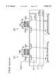
- FIG. 4is a schematic view showing the erase operation of the flash memory in accordance with the present invention.
- a control gate 10b, a source 5b, and a drain 4b in a memory transistor 11b within a non-selected erase block as well as p well region 3 at which memory transistor 11b is formedare being supplied with 0 V, respectively, when a memory transistor 11a within a selected erase block is erased.
- p well region 3 in which the non-selected erase block is arrangedhas a potential fixed to 0 V. Therefore, it is possible to inhibit a well disturbance in the non-selected erase block in the erase operation of the flash memory.
- Control gate 10b, source 5b, and drain 4b of memory transistor 11b within the non-selected erase block and p well regions 3 at which memory transistor 11b is formedmay be in an open state.
- the flash memory in accordance with the present inventioncan inhibit a drain disturbance and a disturbance by a word line in the non-selected erase block when the erase operation is performed.
- main bit line 24is connected to sub bit lines 19a and 19b via the select gate transistor. Therefore, the select gate transistor controls connection/disconnection of main bit line 24 to/from sub bit lines 19a, 19b.
- this select gate transistorcan electrically insulate the non-selected erase block from main bit line 24. That inhibits the drain disturbance in the non-selected erase block when the erase operation is performed.
- control gate (word line) 10extends crossing main bit line 24.
- word lineextends parallel to a longitudinal direction of erase block 26.
- erase block 26is preferably arranged along the entire length of the word line. That is, erase block 26 is preferably defined to include all of a plurality of memory transistors sharing one word line in one erase block 26. In that case, the disturbance by the word line in the non-selected erase block can be effectively inhibited in the erase operation.
- each erase blockcan be almost perfectly isolated electrically in the erase operation of the flash memory.
- a flash memory of high reliabilityis obtained.
- an independent wellis formed for each erase block, so that the well disturbance in the erase operation can be inhibited in a non-selected erase block. Therefore, erroneous operation (erroneous erase) due to the erase operation can be effectively inhibited, and a nonvolatile semiconductor memory device of high reliability is obtained. Also, by forming a well for each erase block as described above, it is possible to simplify a circuit structure related to the erase operation to a greater extent than a conventional example. That reduces the area occupied by circuits related to the erase operation.
- the erase blockcan be replaced by the redundancy block provided that characteristics such as the disturbance are almost same.
- an auxiliary source linecan be formed over the isolating region. It enables reduction in resistance of the source line and improvement in performance of the nonvolatile semiconductor memory device.
Landscapes
- Non-Volatile Memory (AREA)
- Semiconductor Memories (AREA)
- Read Only Memory (AREA)
Abstract
Description
Claims (6)
Applications Claiming Priority (2)
| Application Number | Priority Date | Filing Date | Title |
|---|---|---|---|
| JP8-116480 | 1996-05-10 | ||
| JP11648096AJP3960639B2 (en) | 1996-05-10 | 1996-05-10 | Nonvolatile semiconductor memory device |
Publications (1)
| Publication Number | Publication Date |
|---|---|
| US5994732Atrue US5994732A (en) | 1999-11-30 |
Family
ID=14688159
Family Applications (1)
| Application Number | Title | Priority Date | Filing Date |
|---|---|---|---|
| US08/852,817Expired - LifetimeUS5994732A (en) | 1996-05-10 | 1997-05-07 | Nonvolatile semiconductor memory device |
Country Status (4)
| Country | Link |
|---|---|
| US (1) | US5994732A (en) |
| JP (1) | JP3960639B2 (en) |
| KR (1) | KR100244406B1 (en) |
| TW (1) | TW359900B (en) |
Cited By (18)
| Publication number | Priority date | Publication date | Assignee | Title |
|---|---|---|---|---|
| US6154808A (en)* | 1997-10-31 | 2000-11-28 | Fujitsu Limited | Method and apparatus for controlling data erase operations of a non-volatile memory device |
| US6243292B1 (en) | 2000-01-27 | 2001-06-05 | Mitsubishi Denki Kabushiki Kaisha | Nonvolatile semiconductor memory device capable of reducing memory array area |
| EP1178491A1 (en)* | 2000-08-02 | 2002-02-06 | STMicroelectronics S.r.l. | A semiconductor memory |
| FR2816751A1 (en)* | 2000-11-15 | 2002-05-17 | St Microelectronics Sa | Flash memory erasable by page and method for data storaage, comprising array with counter and sectors, and circuits for reading page address and incrementing counter |
| WO2002015190A3 (en)* | 2000-08-15 | 2003-02-06 | Motorola Inc | Non-volatile memory, method of manufacture and programming |
| US6545310B2 (en)* | 2001-04-30 | 2003-04-08 | Motorola, Inc. | Non-volatile memory with a serial transistor structure with isolated well and method of operation |
| US20030111672A1 (en)* | 2001-12-19 | 2003-06-19 | Cavins Craig A. | Non-volatile memory and method of forming thereof |
| WO2002037502A3 (en)* | 2000-10-30 | 2003-09-25 | Virtual Silicon Technology Inc | Common source eeprom and flash memory |
| US6636441B2 (en)* | 2000-11-15 | 2003-10-21 | Kabushiki Kaisha Toshiba | Semiconductor memory device including non-volatile memory cell array having MOS structure in well region formed on semiconductor substrate |
| US6831860B2 (en)* | 2001-05-23 | 2004-12-14 | Samsung Electronics Co., Ltd. | Nonvolatile semiconductor memory device |
| US20060239111A1 (en)* | 2004-04-21 | 2006-10-26 | Masaki Shingo | Non-volatile semiconductor device and method for automatically recovering erase failure in the device |
| US20070140008A1 (en)* | 2005-12-21 | 2007-06-21 | Microchip Technology Incorporated | Independently programmable memory segments within an NMOS electrically erasable programmable read only memory array achieved by P-well separation and method therefor |
| EP1179849A3 (en)* | 2000-08-09 | 2007-07-11 | Infineon Technologies AG | Memory cell and method of manufacturing |
| US20080247228A1 (en)* | 2007-04-05 | 2008-10-09 | Hao Thai Nguyen | Non-volatile storage with current sensing of negative threshold voltages |
| US20080247241A1 (en)* | 2007-04-05 | 2008-10-09 | Hao Thai Nguyen | Sensing in non-volatile storage using pulldown to regulated source voltage to remove system noise |
| US20100200922A1 (en)* | 2009-02-06 | 2010-08-12 | Ming-Song Sheu | Electrostatic Discharge Protection Device and Method |
| US20120218820A1 (en)* | 2008-04-23 | 2012-08-30 | Hiroshi Maejima | Three dimensional stacked nonvolatile semiconductor memory |
| US20140358076A1 (en)* | 2013-05-28 | 2014-12-04 | Smh Device Corp. | Tunneled Catheter with Hemostasis Mechanism |
Families Citing this family (3)
| Publication number | Priority date | Publication date | Assignee | Title |
|---|---|---|---|---|
| US6147903A (en) | 1997-12-12 | 2000-11-14 | Matsushita Electronics Corporation | Non-volatile semiconductor memory device and method for driving the same |
| US6876582B2 (en)* | 2002-05-24 | 2005-04-05 | Hynix Semiconductor, Inc. | Flash memory cell erase scheme using both source and channel regions |
| JP5466729B2 (en)* | 2012-06-01 | 2014-04-09 | ルネサスエレクトロニクス株式会社 | Nonvolatile semiconductor memory device |
Citations (6)
| Publication number | Priority date | Publication date | Assignee | Title |
|---|---|---|---|---|
| US4878199A (en)* | 1987-02-27 | 1989-10-31 | Kabushiki Kaisha Toshiba | Semiconductor memory device |
| JPH0324762A (en)* | 1989-06-22 | 1991-02-01 | Hitachi Ltd | Semiconductor integrated circuit device |
| JPH03290960A (en)* | 1990-03-30 | 1991-12-20 | Toshiba Corp | Non-volatile semiconductor memory device |
| JPH04352362A (en)* | 1991-05-29 | 1992-12-07 | Rohm Co Ltd | Semiconductor device |
| JPH07161845A (en)* | 1993-12-02 | 1995-06-23 | Nec Corp | Semiconductor nonvolatile memory |
| US5554867A (en)* | 1993-12-27 | 1996-09-10 | Mitsubishi Denki Kabushiki Kaisha | Nonvolatile semiconductor memory device having a memory cell transistor and a select transistor |
- 1996
- 1996-05-10JPJP11648096Apatent/JP3960639B2/ennot_activeExpired - Lifetime
- 1997
- 1997-05-07USUS08/852,817patent/US5994732A/ennot_activeExpired - Lifetime
- 1997-05-07KRKR1019970017492Apatent/KR100244406B1/ennot_activeExpired - Fee Related
- 1997-05-08TWTW086106138Apatent/TW359900B/ennot_activeIP Right Cessation
Patent Citations (6)
| Publication number | Priority date | Publication date | Assignee | Title |
|---|---|---|---|---|
| US4878199A (en)* | 1987-02-27 | 1989-10-31 | Kabushiki Kaisha Toshiba | Semiconductor memory device |
| JPH0324762A (en)* | 1989-06-22 | 1991-02-01 | Hitachi Ltd | Semiconductor integrated circuit device |
| JPH03290960A (en)* | 1990-03-30 | 1991-12-20 | Toshiba Corp | Non-volatile semiconductor memory device |
| JPH04352362A (en)* | 1991-05-29 | 1992-12-07 | Rohm Co Ltd | Semiconductor device |
| JPH07161845A (en)* | 1993-12-02 | 1995-06-23 | Nec Corp | Semiconductor nonvolatile memory |
| US5554867A (en)* | 1993-12-27 | 1996-09-10 | Mitsubishi Denki Kabushiki Kaisha | Nonvolatile semiconductor memory device having a memory cell transistor and a select transistor |
Non-Patent Citations (4)
| Title |
|---|
| "A Novel Cell Structure Suitable For A 3 Volt Operation, Sector Erase Flash Memory", H. Onoda et al., IEDM 92 pp. 599-602. |
| "Improved Array Architectures . . .", Hiroshi Onoda et al. IEICE Trans. Electron., vol. E77-C No. 8 Aug. 1994, pp. 1279-1286. |
| A Novel Cell Structure Suitable For A 3 Volt Operation, Sector Erase Flash Memory , H. Onoda et al., IEDM 92 pp. 599 602.* |
| Improved Array Architectures . . . , Hiroshi Onoda et al. IEICE Trans. Electron., vol. E77 C No. 8 Aug. 1994, pp. 1279 1286.* |
Cited By (36)
| Publication number | Priority date | Publication date | Assignee | Title |
|---|---|---|---|---|
| US6154808A (en)* | 1997-10-31 | 2000-11-28 | Fujitsu Limited | Method and apparatus for controlling data erase operations of a non-volatile memory device |
| US6243292B1 (en) | 2000-01-27 | 2001-06-05 | Mitsubishi Denki Kabushiki Kaisha | Nonvolatile semiconductor memory device capable of reducing memory array area |
| EP1178491A1 (en)* | 2000-08-02 | 2002-02-06 | STMicroelectronics S.r.l. | A semiconductor memory |
| US6532171B2 (en) | 2000-08-02 | 2003-03-11 | Stmicroelectronics S.R.L. | Nonvolatile semiconductor memory capable of selectively erasing a plurality of elemental memory units |
| EP1179849A3 (en)* | 2000-08-09 | 2007-07-11 | Infineon Technologies AG | Memory cell and method of manufacturing |
| KR100762114B1 (en) | 2000-08-15 | 2007-10-02 | 프리스케일 세미컨덕터, 인크. | Nonvolatile Memory, Manufacturing and Programming Methods |
| CN1327526C (en)* | 2000-08-15 | 2007-07-18 | 自由度半导体公司 | Programming Method of Electrically Erasable Programmable Read-Only Memory Array |
| WO2002015190A3 (en)* | 2000-08-15 | 2003-02-06 | Motorola Inc | Non-volatile memory, method of manufacture and programming |
| WO2002037502A3 (en)* | 2000-10-30 | 2003-09-25 | Virtual Silicon Technology Inc | Common source eeprom and flash memory |
| USRE40976E1 (en) | 2000-10-30 | 2009-11-17 | Albert Bergemont | Common source EEPROM and flash memory |
| WO2002041322A1 (en)* | 2000-11-15 | 2002-05-23 | Stmicroelectronics Sa | Page-erasable flash memory |
| US6636441B2 (en)* | 2000-11-15 | 2003-10-21 | Kabushiki Kaisha Toshiba | Semiconductor memory device including non-volatile memory cell array having MOS structure in well region formed on semiconductor substrate |
| US20040017722A1 (en)* | 2000-11-15 | 2004-01-29 | Stmicroelectronics Sa | Page-erasable flash memory |
| US6807103B2 (en) | 2000-11-15 | 2004-10-19 | Stmicroelectronics S.A. | Page-erasable flash memory |
| FR2816751A1 (en)* | 2000-11-15 | 2002-05-17 | St Microelectronics Sa | Flash memory erasable by page and method for data storaage, comprising array with counter and sectors, and circuits for reading page address and incrementing counter |
| US6545310B2 (en)* | 2001-04-30 | 2003-04-08 | Motorola, Inc. | Non-volatile memory with a serial transistor structure with isolated well and method of operation |
| US6831860B2 (en)* | 2001-05-23 | 2004-12-14 | Samsung Electronics Co., Ltd. | Nonvolatile semiconductor memory device |
| WO2003054965A3 (en)* | 2001-12-19 | 2004-03-04 | Motorola Inc | Non-volatile memory and method of forming thereof |
| US20030111672A1 (en)* | 2001-12-19 | 2003-06-19 | Cavins Craig A. | Non-volatile memory and method of forming thereof |
| CN1316625C (en)* | 2001-12-19 | 2007-05-16 | 自由度半导体公司 | Nonvolatile memory and method of manufacturing the same |
| US20060239111A1 (en)* | 2004-04-21 | 2006-10-26 | Masaki Shingo | Non-volatile semiconductor device and method for automatically recovering erase failure in the device |
| US7352620B2 (en)* | 2004-04-21 | 2008-04-01 | Spansion Llc | Non-volatile semiconductor device and method for automatically recovering erase failure in the device |
| WO2007078614A1 (en)* | 2005-12-21 | 2007-07-12 | Microchip Technology Incorporated | Independently programmable memory segment within an nmos electrically erasable programmable read only memory array achived by p-well separation and methods for programming |
| US20070140008A1 (en)* | 2005-12-21 | 2007-06-21 | Microchip Technology Incorporated | Independently programmable memory segments within an NMOS electrically erasable programmable read only memory array achieved by P-well separation and method therefor |
| US7532516B2 (en) | 2007-04-05 | 2009-05-12 | Sandisk Corporation | Non-volatile storage with current sensing of negative threshold voltages |
| US20080247241A1 (en)* | 2007-04-05 | 2008-10-09 | Hao Thai Nguyen | Sensing in non-volatile storage using pulldown to regulated source voltage to remove system noise |
| US7447079B2 (en)* | 2007-04-05 | 2008-11-04 | Sandisk Corporation | Method for sensing negative threshold voltages in non-volatile storage using current sensing |
| US20080247238A1 (en)* | 2007-04-05 | 2008-10-09 | Hao Thai Nguyen | Method for sensing negative threshold voltages in non-volatile storage using current sensing |
| US7606076B2 (en) | 2007-04-05 | 2009-10-20 | Sandisk Corporation | Sensing in non-volatile storage using pulldown to regulated source voltage to remove system noise |
| US20080247228A1 (en)* | 2007-04-05 | 2008-10-09 | Hao Thai Nguyen | Non-volatile storage with current sensing of negative threshold voltages |
| US20120218820A1 (en)* | 2008-04-23 | 2012-08-30 | Hiroshi Maejima | Three dimensional stacked nonvolatile semiconductor memory |
| US8693250B2 (en)* | 2008-04-23 | 2014-04-08 | Kabushiki Kaisha Toshiba | Three dimensional stacked nonvolatile semiconductor memory |
| US20100200922A1 (en)* | 2009-02-06 | 2010-08-12 | Ming-Song Sheu | Electrostatic Discharge Protection Device and Method |
| US8378422B2 (en)* | 2009-02-06 | 2013-02-19 | Taiwan Semiconductor Manufacturing Company, Ltd. | Electrostatic discharge protection device comprising a plurality of highly doped areas within a well |
| US20140358076A1 (en)* | 2013-05-28 | 2014-12-04 | Smh Device Corp. | Tunneled Catheter with Hemostasis Mechanism |
| US9308351B2 (en)* | 2013-05-28 | 2016-04-12 | Smh Device Corp. | Tunneled catheter with hemostasis mechanism |
Also Published As
| Publication number | Publication date |
|---|---|
| JP3960639B2 (en) | 2007-08-15 |
| JPH09307005A (en) | 1997-11-28 |
| KR970077636A (en) | 1997-12-12 |
| TW359900B (en) | 1999-06-01 |
| KR100244406B1 (en) | 2000-02-01 |
Similar Documents
| Publication | Publication Date | Title |
|---|---|---|
| US5994732A (en) | Nonvolatile semiconductor memory device | |
| JP4252464B2 (en) | Refresh method for dynamic page program | |
| US7773429B2 (en) | Non-volatile memory device and driving method thereof | |
| KR0172016B1 (en) | Nonvolatile Semiconductor Memory with Programming Area for Injection and Extraction of Carrier to and from the Floating Gate | |
| US7573742B2 (en) | Nonvolatile semiconductor memory | |
| US4514830A (en) | Defect-remediable semiconductor integrated circuit memory and spare substitution method in the same | |
| US7423912B2 (en) | SONOS memory array with improved read disturb characteristic | |
| KR100187196B1 (en) | Nonvolatile Semiconductor Memory Device | |
| KR20040068552A (en) | Semiconductor device having a byte-erasable eeprom memory | |
| US5559735A (en) | Flash memory having select transistors | |
| US5500816A (en) | Non-volatile semiconductor memory device and manufacturing method thereof | |
| US20080123430A1 (en) | Non-volatile memory unit and array | |
| US7457154B2 (en) | High density memory array system | |
| US7272040B2 (en) | Multi-bit virtual-ground NAND memory device | |
| JP4060938B2 (en) | Nonvolatile semiconductor memory device | |
| JP2005197624A (en) | Nonvolatile storage | |
| US20090027942A1 (en) | Semiconductor memory unit and array | |
| US7355893B2 (en) | Semiconductor memory device and method for writing to semiconductor memory device | |
| US6323517B1 (en) | Non-volatile memory device with single-layered overwriting transistor | |
| US6888753B2 (en) | Memory cell array comprising individually addressable memory cells and method of making the same | |
| US6011717A (en) | EEPROM memory programmable and erasable by Fowler-Nordheim effect | |
| US6347053B1 (en) | Nonviolatile memory device having improved threshold voltages in erasing and programming operations | |
| US5592000A (en) | Non-volatile semiconductor memory device programmable and erasable at low voltage | |
| US7042767B2 (en) | Flash memory unit and method of programming a flash memory device | |
| US6291843B1 (en) | Semiconductor memory device |
Legal Events
| Date | Code | Title | Description |
|---|---|---|---|
| AS | Assignment | Owner name:HITACHI ULSI ENGINEERING CORPORATION, JAPAN Free format text:ASSIGNMENT OF ASSIGNORS INTEREST;ASSIGNORS:AJIKA, NATSUO;MATSUO, AKINORI;REEL/FRAME:008548/0358 Effective date:19970422 Owner name:MITSUBISHI DENKI KABUSHIKI KAISHA, JAPAN Free format text:ASSIGNMENT OF ASSIGNORS INTEREST;ASSIGNORS:AJIKA, NATSUO;MATSUO, AKINORI;REEL/FRAME:008548/0358 Effective date:19970422 Owner name:HITACHI, LTD., JAPAN Free format text:ASSIGNMENT OF ASSIGNORS INTEREST;ASSIGNORS:AJIKA, NATSUO;MATSUO, AKINORI;REEL/FRAME:008548/0358 Effective date:19970422 | |
| AS | Assignment | Owner name:BAYER AKTIENGESELLSCHAFT, GERMANY Free format text:ASSIGNMENT OF ASSIGNORS INTEREST;ASSIGNORS:LINKER, KARL-HEINZ;FINDEISEN, KURT;HAAS, WILHELM;AND OTHERS;REEL/FRAME:008946/0265;SIGNING DATES FROM 19970919 TO 19971017 | |
| STCF | Information on status: patent grant | Free format text:PATENTED CASE | |
| FEPP | Fee payment procedure | Free format text:PAYOR NUMBER ASSIGNED (ORIGINAL EVENT CODE: ASPN); ENTITY STATUS OF PATENT OWNER: LARGE ENTITY | |
| CC | Certificate of correction | ||
| FPAY | Fee payment | Year of fee payment:4 | |
| FPAY | Fee payment | Year of fee payment:8 | |
| AS | Assignment | Owner name:RENESAS ELECTRONICS CORPORATION, JAPAN Free format text:ASSIGNMENT OF ASSIGNORS INTEREST;ASSIGNOR:HITACHI, LTD.;REEL/FRAME:025981/0287 Effective date:20110307 Owner name:RENESAS ELECTRONICS CORPORATION, JAPAN Free format text:ASSIGNMENT OF ASSIGNORS INTEREST;ASSIGNOR:MITSUBISHI DENKI KABUSHIKI KAISHA;REEL/FRAME:025980/0219 Effective date:20110307 | |
| FPAY | Fee payment | Year of fee payment:12 |