US5991698A - Electrical lap guide data acquisition unit and measurement scheme - Google Patents
Electrical lap guide data acquisition unit and measurement schemeDownload PDFInfo
- Publication number
- US5991698A US5991698AUS08/852,434US85243497AUS5991698AUS 5991698 AUS5991698 AUS 5991698AUS 85243497 AUS85243497 AUS 85243497AUS 5991698 AUS5991698 AUS 5991698A
- Authority
- US
- United States
- Prior art keywords
- acquisition unit
- data acquisition
- resistors
- analog
- current sources
- Prior art date
- Legal status (The legal status is an assumption and is not a legal conclusion. Google has not performed a legal analysis and makes no representation as to the accuracy of the status listed.)
- Expired - Fee Related
Links
Images


Classifications
- G—PHYSICS
- G11—INFORMATION STORAGE
- G11B—INFORMATION STORAGE BASED ON RELATIVE MOVEMENT BETWEEN RECORD CARRIER AND TRANSDUCER
- G11B5/00—Recording by magnetisation or demagnetisation of a record carrier; Reproducing by magnetic means; Record carriers therefor
- G11B5/127—Structure or manufacture of heads, e.g. inductive
- G11B5/31—Structure or manufacture of heads, e.g. inductive using thin films
- G11B5/3103—Structure or manufacture of integrated heads or heads mechanically assembled and electrically connected to a support or housing
- H—ELECTRICITY
- H01—ELECTRIC ELEMENTS
- H01L—SEMICONDUCTOR DEVICES NOT COVERED BY CLASS H10
- H01L21/00—Processes or apparatus adapted for the manufacture or treatment of semiconductor or solid state devices or of parts thereof
- G—PHYSICS
- G11—INFORMATION STORAGE
- G11B—INFORMATION STORAGE BASED ON RELATIVE MOVEMENT BETWEEN RECORD CARRIER AND TRANSDUCER
- G11B5/00—Recording by magnetisation or demagnetisation of a record carrier; Reproducing by magnetic means; Record carriers therefor
- G11B5/127—Structure or manufacture of heads, e.g. inductive
- G11B5/187—Structure or manufacture of the surface of the head in physical contact with, or immediately adjacent to the recording medium; Pole pieces; Gap features
- G11B5/1871—Shaping or contouring of the transducing or guiding surface
- G—PHYSICS
- G11—INFORMATION STORAGE
- G11B—INFORMATION STORAGE BASED ON RELATIVE MOVEMENT BETWEEN RECORD CARRIER AND TRANSDUCER
- G11B5/00—Recording by magnetisation or demagnetisation of a record carrier; Reproducing by magnetic means; Record carriers therefor
- G11B5/127—Structure or manufacture of heads, e.g. inductive
- G11B5/31—Structure or manufacture of heads, e.g. inductive using thin films
- G11B5/3163—Fabrication methods or processes specially adapted for a particular head structure, e.g. using base layers for electroplating, using functional layers for masking, using energy or particle beams for shaping the structure or modifying the properties of the basic layers
- G11B5/3166—Testing or indicating in relation thereto, e.g. before the fabrication is completed
- Y—GENERAL TAGGING OF NEW TECHNOLOGICAL DEVELOPMENTS; GENERAL TAGGING OF CROSS-SECTIONAL TECHNOLOGIES SPANNING OVER SEVERAL SECTIONS OF THE IPC; TECHNICAL SUBJECTS COVERED BY FORMER USPC CROSS-REFERENCE ART COLLECTIONS [XRACs] AND DIGESTS
- Y10—TECHNICAL SUBJECTS COVERED BY FORMER USPC
- Y10T—TECHNICAL SUBJECTS COVERED BY FORMER US CLASSIFICATION
- Y10T29/00—Metal working
- Y10T29/49—Method of mechanical manufacture
- Y10T29/49002—Electrical device making
- Y10T29/49004—Electrical device making including measuring or testing of device or component part
- Y—GENERAL TAGGING OF NEW TECHNOLOGICAL DEVELOPMENTS; GENERAL TAGGING OF CROSS-SECTIONAL TECHNOLOGIES SPANNING OVER SEVERAL SECTIONS OF THE IPC; TECHNICAL SUBJECTS COVERED BY FORMER USPC CROSS-REFERENCE ART COLLECTIONS [XRACs] AND DIGESTS
- Y10—TECHNICAL SUBJECTS COVERED BY FORMER USPC
- Y10T—TECHNICAL SUBJECTS COVERED BY FORMER US CLASSIFICATION
- Y10T29/00—Metal working
- Y10T29/49—Method of mechanical manufacture
- Y10T29/49002—Electrical device making
- Y10T29/4902—Electromagnet, transformer or inductor
- Y10T29/49021—Magnetic recording reproducing transducer [e.g., tape head, core, etc.]
- Y10T29/49032—Fabricating head structure or component thereof
- Y10T29/49036—Fabricating head structure or component thereof including measuring or testing
- Y10T29/49037—Using reference point/surface to facilitate measuring
Definitions
- the present inventionrelates generally to the batch fabrication of sliders which carry magnetoresistive (MR) and/or inductive transducers for data storage applications. More particularly, the present invention relates to the measurement of electrical lap guide (ELG) resistors which guide the lapping process such that the head sliders in a row or bar are machined to a specified transducer height.
- MRmagnetoresistive
- ELGelectrical lap guide
- Magnetic read/write transducersare produced using thin film deposition techniques.
- an array of transducersare formed on a common substrate.
- the substrateis sliced to produce bars, with one row of transducers in a side-by-side pattern on each bar.
- the barsare then machined or lapped to establish a desired MR transducer height (sometimes referred to as a stripe height SH) or a desired inductive transducer height (sometimes referred to as a throat height TH).
- a desired MR transducer heightsometimes referred to as a stripe height SH
- a desired inductive transducer heightsometimes referred to as a throat height TH
- ELGsfor this and other purposes are well known in the art. See for example, U.S. Pat. No. 5,023,991 entitled ELECTRICAL GUIDE FOR TIGHT TOLERANCE MACHINING, which issued to Alan Smith on Jun. 18, 1991.
- One common practiceis to use ELGs and a feedback controlled bending mechanism to form a closed-loop lapping process. ELG measurement accuracy, noise and resolution directly affect finished slider SH and TH variation. As the data storage industry is continuously driven by higher density and lower cost requirements, the transducer height tolerance continues to decrease, while the number of head sliders per bar increases, leading to thinner and more flexible bars. To maintain and improve transducer height control during the lapping process, more accurate ELG measurement and monitoring techniques are required.
- ELG'stypically include three resistive components, but can contain a greater or lesser number if desired. Frequently, as many as 14 ELGs are included per bar. Therefore, a great number of resistances must be measured during lapping.
- DAUsdata acquisition units
- the single current sourceis directed by the multiplexer to excite the component.
- the corresponding voltage signalis connected to the signal processing channel by the multiplexer and is amplified, filtered and digitized
- the digitized resistance readingis then stored in the memory of the control computer. This procedure is repeated through time multiplexing, with the single current source exciting one resistive element at time, through switching or multiplexing, to read all of the ELG resistive elements.
- ELG resistance readings using conventional DAUsare not independent of other ELG resistance readings.
- the current source, voltmeter and filterhave to be switched from resistive element to resistive element through multiplexing. Since the current source and the filters need time to settle after switching from one ELG measurement to the next, significant quantities of noise are introduced into the measurement signal if too many resistive elements are monitored, thus limiting the time available. Other sources of noise which effect the measurement accuracy are caused by the mechanical bending portions of the system.
- a lapping system data acquisition unit of the present inventionthat is disclosed for use in measuring resistances of multiple resistors embedded in a structure to be machined.
- Each of multiple independent current sourcesdirects a current through one of the multiple resistors embedded in the structure during machining of a surface of the structure.
- Each of multiple voltage sensing devicescouples to a separate one of the multiple resistors and provides a separate analog voltage output signal indicative of the resistance of the resistor.
- Each of multiple filtersis coupled to a separate one of the multiple voltage sensing devices.
- Analog-to-digital conversion circuitry coupled to the multiple filtersgenerates a digitized signal for each of the filtered output signals.
- FIG. 1is a perspective view of a row or bar of head sliders which can be lapped to obtain a desired transducer height using the system of the present invention.
- FIG. 2is perspective view of a completed head slider obtained by dicing the bar of head sliders illustrated in FIG. 1.
- FIG. 3is a view of a prior art lapping system DAU which is conventionally used to monitor/control the lapping process.
- FIG. 4is a schematic illustration of a portion of an improved lapping system DAU in accordance with preferred embodiments of the present invention.
- FIG. 5is a diagrammatic illustration of a portion of the lapping system DAU illustrated in FIG. 4.
- FIG. 6is a diagrammatic illustration of one embodiment of the lapping system DAU of the present invention.
- FIG. 7is a diagrammatic illustration of a portion of an alternate embodiment of the lapping system DAU of the present invention.
- the present inventionincludes DAUs which are particularly adapted for monitoring resistances of ELG elements on a bar of head sliders being machined to achieve a desired transducer height.
- the DAUs and measurement schemes of the present inventioncan be employed to monitor the resistances of multiple ELG resistors used to control any of a wide variety of machining processes.
- FIG. 1is a perspective view illustrating bar 10 which contains an array of head sliders 15.
- bar 10is typically mounted on a lapping system work piece (not shown) for lapping to achieve a desired transducer height.
- a lapping system DAUis coupled to the resistive elements of ELG's located within bar 10 to control the lapping process.
- FIG. 3is a diagrammatic illustration of a conventional DAU and measurement scheme of the type typically used in lapping systems to control machining of bar 10 of head sliders.
- Bar 10is mounted on a carrier on arm 20 of a lapping machine during lapping.
- bar 10contains multiple ELGs (ELG1 through ELGN) for use in controlling the lapping process to achieve a desired transducer height.
- ELGsELGs
- each of the ELG's in this exampleinclude three resistors.
- Resistor R N1 (where N designates which of the N ELGs is being referred to) of each ELGis typically an analog resistor which is exposed to the machined surface during lapping such that its resistance is changed by the machining process.
- Reference resistors R N2 and R N3can be monitored and used to calculate local sheet resistance Q, prior to lapping, which can then be combined with the measured resistance of resistor R N1 to estimate the transducer height.
- monitoring reference resistor R N3 during lappingallows compensation for resistance measurement variations caused by thermal effects or other sources. It is generally not necessary to continuously monitor reference resistors R N2 during lapping. Therefore, after measuring reference resistors R N2 prior to lapping in order to calculate local sheet resistance Q, these reference resistors need only be monitored occasionally, if at all. It must be noted that ELGs and measurement schemes having more or less than three resistors can be used. The reference resistors of each ELG are accessed via bond pads or terminals 30 on a surface of bar 10. Using conventional measurement techniques, two leads 25 are required for each ELG resistive element. Thus, a total of 6N leads are required and are connectable through 6N wires in cable 35 to DAU 40.
- DAU 40 and the corresponding measurement scheme typically used in the prior artinclude single current source 50, multiplexer 45, amplifier 55, filter 60 and analog-to-digital (A/D) converter 65.
- A/Danalog-to-digital
- To measure the resistance of one of the resistive elements of one of the ELGScurrent from current source 50 is directed by multiplexer 45 to excite the particular ELG resistor.
- the resulting voltage signalis connected through cable 35 and multiplexer 45 to amplifier 55, filter 60 and A/D converter 65.
- the digitized resistance representative voltage readingis then stored in the memory of remote computer 70. This procedure is repeated in a time multiplexed fashion to monitor the resistances of all desired ELG elements during lapping.
- this conventional DAU format and measurement schemeintroduces a number of problems.
- this schemeresults in significant coupling/cross-talk of resistance measurement signals.
- ELG resistance readings using this schemeare not independent.
- current source 50has to be switched from channel to channel to the desired ELG resistive elements through multiplexing.
- low pass filter 60with a corresponding cut-off frequency, requires a certain amount of settling time. Without sufficient settling time, cross-talk affects the signals provided to A/D converter 65.
- a second problem with the conventional scheme illustrated in FIG. 3relates to process noise.
- Lappingis a relatively slow process.
- To accurately measure ELG resistancesit is desired to filter out high frequency noise in the measurement signals.
- the scheme illustrated in FIG. 3is not able to meet this requirement because sampling occurs when the current source is switched from one channel to the next. The result is that some mechanical process noise components remain in the measurement signals and ultimately effect the lapping accuracy.
- a third problemrelates to aliasing.
- Sampling theoremrequires that the sampling rate ( ⁇ ) be greater than twice the signal bandwidth. Otherwise, any frequency components in the signal above ⁇ /2 are "folded" about this frequency due to overlap of the shifted versions of the signal spectrum. Thus, the signal cannot be completely recovered from its sample.
- samplingactually happens when the current source and voltmeter (amplifier 55) are switched to read R N1 , R N2 and R N3 in different ELG's. Anti-aliasing filtering cannot be implemented. As a result, noise in ELG signals may exist due to aliasing.
- a fourth problem with the scheme illustrated in FIG. 3relates to a resulting low signal-to-noise ratio (SNR).
- the electronics configurationnormally requires a long cable 35 to connect all of the ELG leads 25 on arm 20 to DAU 40 in the remote control box. This tends to introduce more noise to already typically low ELG signal amplitudes.
- a fifth problemrelates the limited number of channels available. Current DAU's normally monitor as many as fourteen ELG's. As bars are getting thinner and the number of sliders per bar higher, slider transducer height profiles across the bar can vary significantly. To maintain and improve transducer height control, more channels are needed in the ELG DAU. This increases the number of wires needed in cable 35.
- FIG. 4is a schematic illustration of an improved ELG measurement scheme which is implemented using DAU 100 of the present invention. Illustrated in FIG. 4 are 2 ELGs, ELG1 and ELG2, out of the N ELGs on bar 10. While only two ELGs are illustrated, the concepts are readily implemented with all N ELGs.
- an independent current source and signal processing channeli.e. voltmeters or amplifiers, and filters
- each individual ELG resistor elementto be measured relatively continuously throughout the lapping process.
- switches S1, S2, S3 and S4are controlled in order to substantially constantly excite ELG resistive elements R 11 l, R 13 , R 21 and R 23 .
- Voltmeters V1, V2, V3 and V4are then used to measure, on a substantially constant basis, the voltage drops across resistors R 11 , R 13 , R 21 and R 31 , respectively.
- Resistances of resistive elements R 12 and R 22are preferably measured at a low sampling rate to minimize switching effects.
- reference resistors R 12 and R 22which are not exposed to machining and which are not supposed to change in value, can be measured once immediately after lapping begins by closing switches S1 and S3 and measuring the voltages with voltmeters V2 and V4.
- the resistance of reference resistor R 12is equal to voltage V2 divided by current I1.
- the resistance of reference resistor R 22is equal to voltage V4 divided by current I3.
- Switches S2 and S4are then closed and voltages V1, V2, V3 and V4 are sampled at the desired rate throughout the lapping process to measure resistors R 11 , R 13 , R 21 , R 23 .
- resistances R N1 and R N3 for other ELGscan be determined in a similar manner using additional current sources, voltmeters and switches.
- the resistances of resistors R N2can be sampled at a much slower rate during lapping to compensate for process related resistance variations such as thermal effects.
- Measurement accuracyis dependent upon current source calibration and stability ( ⁇ 10 ppm), current leakage to the voltmeters ( ⁇ 1 nA), and current leakage to switches ( ⁇ 1 nA).
- Each voltmeterrepresents an instrumentation amplifier with high impedance (>10 10 ohms), high channel isolation (>100 dB) and a differential input.
- FIG. 5is a diagrammatic illustration of a portion of DAU 200 in accordance with the present invention.
- FIG. 5illustrates only one resistive element out of the multiple resistive elements of the N ELGs on bar 10. Therefore, FIG. 5 also only illustrates the DAU channel having single current source 205, voltmeter or amplifier 210, filter 215 and A/D converter 220. However, it is clear that DAU 200 will have multiple independent current sources, voltmeters, filters and A/D converters to measure the resistances of the multiple resistive element on bar 10. Additionally, FIG. 5 illustrates DAU 200 positioned on arm 20 which is also where the carrier on which bar 10 is mounted is located.
- ELG resistive elements R Ni(where N represents the ELG number, and where i represents which of the resistors of the particular ELG is being monitored) has independent current source 205 of DAU 200 coupled in series such that current from current source 205 excites resistive element R Ni substantially continuously during the lapping process.
- Dedicated amplifier 210has inputs which are connected across resistor R Ni and provides as an output a resistance dependent voltage signal.
- Filter 215filters the signal before providing it to A/D converter 220. As discussed previously, because the signal provided to filter 215 is not a sampled signal indicative of resistances of many ELG resistors, the cutoff frequencies of filter 215 can be chosen to optimize the reduction of noise in the signal. This is also a departure from the prior art where the sampling rate dictates the filter characteristics.
- A/D converter 220provides as an output a digitized signal representative of the resistance of resistor R Ni . This is also a departure from conventional DAUs in that the resistance signals are digitized on arm 20, as opposed to at a remote location.
- DAU 200includes floating (non-grounded) power supply 225 in order to minimize current leakage and the introduction of ground noise. Typically, floating power supply 225 will be an isolated DC-to-DC converter.
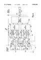
- FIG. 6is a schematic illustration of DAU 300 in accordance with preferred embodiments of the present invention.
- DAU 300is substantially the same or similar to DAU 200, but illustrates the independent current sources, amplifiers and filters used to monitor multiple ELG resistive elements. Also, DAU 300 both illustrates individual features of DAU 200 in greater detail, and includes parallel to serial converter 310. DAU 300 is mounted on arm 20 and the ELG readings are digitized on the arm to eliminate the noise and errors that would be introduced by cabling to a remote DAU. DAU 300 also includes calibration features not shown in DAUs 100 and 200.
- bar 10includes N three resistor ELGs for use in monitoring and controlling lapping of bar 10 to achieve a desired transducer height.
- the resistive elements of the ELGs on bar 10are accessed through bond pads 30 on the surface of bar 10.
- current source I1is normally connected in series with resistor R 11 when switch S1 is closed.
- switches S2, S3 and S4 closedcurrent sources I2, I3 and I4 are usually connected in series with respective one of resistors R 13 , R 21 and R 23 .
- DAU 300functions the same as DAU 100 discussed above with reference to FIG. 4.
- switches S1, S2, S3 and S4are controllable to measure the resistances of resistors R 12 and R 22 .
- DAU 300functions substantially as described above with reference to FIGS. 4 and 5.
- DAU 300includes amplifiers 210, filters 215, A/D convertors 220 and parallel to serial convertor 310.
- Amplifiers 210are preferably a series of individual amplifiers 211 and 212 each operating in a differential amplifier configuration.
- Amplifiers 211are used to measure resistances of ELG resistors R Ni as previously discussed.
- Amplifiers 212are used to measure the resistances of calibration resistors R C .
- Filters 215include a series of filters 216 and 217. Filters 216 are coupled to the outputs of amplifiers 211, while filters 217 are coupled to the output of amplifiers 212.
- Filters 215are preferably low pass filters, which perform an anti-aliasing function.
- the cutoff frequencies of filters 215can be chosen based upon the band width of the signals being filtered, as opposed to being chosen based upon the sampling rate as was the case in the prior art.
- A/D converters 220are preferably four channel A/D converters (typically Delta-Sigma A/D devices), having greater than 16 bit resolution, programmable gain, internal digital filtering and self-calibration. However, other D/A conversion circuitry can be used.
- Parallel to serial converter 310receives the digitized measurement signal from A/D convertors 220 and converts multiple digitized signals into a signal serial bit stream for communication through cable 312 to a remotely positioned computer or controller 70.
- Each ELG signal acquisition channelincludes an analog interface and a four channel A/D converter 220.
- the analog interfaceincludes two isolated current sources (for example current sources I1 and I2), two calibration resistors R C , four switches (for example, switches S1, S2, S5 and S6) and four subchannels (i.e. two combinations of amplifiers 211 and filters 216, and two combinations of amplifiers 212 and filters 217) for amplifying and filtering measured analog signals.
- DAU 300differs from DAUs 100 and 200 in that it includes calibration resistors R C , as well as amplifiers 212 and filters 217 for amplifying and filtering the calibration measurement signal.
- calibration resistors R CAs an example of the manner in which DAU 300 is calibrated, for the DAU channel corresponding to ELG 1, switches S1 and S2 are opened while switches S5 and S6 are closed. This provides currents I1 and I2 to calibration resistors R C . The voltage drops across these calibration resistors are amplified by amplifiers 212 and filtered by filters 217.
- the calibration resistance measurement signalsare converted to digital signals by A/D converters 220, serialized by converter 310 and provided for calibration to computer 70.
- the resistances or resistors R N1 , R N2 , R N3are determined by controlling the corresponding switches in the same manner as described above with reference to DAU 100 shown in FIG. 4.
- FIG. 7illustrates an alternative DAU based upon the proposed invention, but which reduces the number of amplifiers, filters and A/D converters required. However, using this embodiment, switch-on effects are included in the resistance measurements.
- DAU 400is illustrated diagrammatically in the format of FIG. 4. However, DAU 400 will be implemented like, and share most of the features with, DAU 300 illustrated in FIG. 6.
- FIG. 7illustrates two channels of DAU 400, channel 410 for measuring resistances of ELG1 and channel 420 for measuring resistances of ELG2.
- DAU 400cuts the number or amplifiers 210, as well as the number filters and A/D converters (not shown), in half by controlling switches S9, S10, S11, S12, S13, S14 and S15 to provide the desired measurement signals to amplifiers 210. In this way, instead of having a separate amplifier and filter for the calibration resistors, calibration and lapping resistor measurements use the same channels.
- the DAUs of the present inventionprovides numerous advantages over the prior art. By including dedicated current sources and voltage sensing circuitry for measuring the resistances of ELG resistors on a substantially constant basis, the switching effects experienced in the prior art are minimized or eliminated. Further, by positioning the DAUs of the present invention on the arm which supports the machined object, digitized signals can be transmitted to the remote computer controlling the process. This greatly improves the signal-to-noise ratio and therefore minimizes errors. Further, by including a parallel to serial converter, far less electrical connections are needed in the cabling between the DAU and the remote computer, as compared to the number of wires required in the cabling between prior art DAUs and the ELGs on the structure being machined. Further, since switching between channels is greatly reduced, the filters of the DAUs of the present invention can be selected for their ability to reduce noise. This was frequently not the case in conventional DAU designs.
Landscapes
- Engineering & Computer Science (AREA)
- Manufacturing & Machinery (AREA)
- Physics & Mathematics (AREA)
- Condensed Matter Physics & Semiconductors (AREA)
- General Physics & Mathematics (AREA)
- Computer Hardware Design (AREA)
- Microelectronics & Electronic Packaging (AREA)
- Power Engineering (AREA)
- Measurement Of Resistance Or Impedance (AREA)
Abstract
Description
Claims (20)
Priority Applications (1)
| Application Number | Priority Date | Filing Date | Title |
|---|---|---|---|
| US08/852,434US5991698A (en) | 1997-01-29 | 1997-05-07 | Electrical lap guide data acquisition unit and measurement scheme |
Applications Claiming Priority (2)
| Application Number | Priority Date | Filing Date | Title |
|---|---|---|---|
| US3656797P | 1997-01-29 | 1997-01-29 | |
| US08/852,434US5991698A (en) | 1997-01-29 | 1997-05-07 | Electrical lap guide data acquisition unit and measurement scheme |
Publications (1)
| Publication Number | Publication Date |
|---|---|
| US5991698Atrue US5991698A (en) | 1999-11-23 |
Family
ID=26713283
Family Applications (1)
| Application Number | Title | Priority Date | Filing Date |
|---|---|---|---|
| US08/852,434Expired - Fee RelatedUS5991698A (en) | 1997-01-29 | 1997-05-07 | Electrical lap guide data acquisition unit and measurement scheme |
Country Status (1)
| Country | Link |
|---|---|
| US (1) | US5991698A (en) |
Cited By (13)
| Publication number | Priority date | Publication date | Assignee | Title |
|---|---|---|---|---|
| US6047224A (en)* | 1996-04-10 | 2000-04-04 | Seagate Techology, Inc. | Machining guide for magnetic recording reproduce heads |
| US6193584B1 (en)* | 1999-05-27 | 2001-02-27 | Read-Rite Corporation | Apparatus and method of device stripe height control |
| US6330488B1 (en)* | 1997-11-12 | 2001-12-11 | Tdk Corporation | Method for controlling machining process of workpiece |
| US6370763B1 (en)* | 1997-04-10 | 2002-04-16 | Fujitsu Limited | Manufacturing method for magnetic heads |
| US6532646B2 (en)* | 1998-08-25 | 2003-03-18 | Fujitsu Limited | Method of manufacturing magnetic head |
| US6602109B1 (en)* | 1998-12-16 | 2003-08-05 | University Of Massachusetts | Grinding wheel system |
| US6684171B2 (en) | 2002-04-22 | 2004-01-27 | International Business Machines Corporation | In-situ stripe height calibration of magneto resistive sensors |
| US6736704B2 (en) | 2002-04-18 | 2004-05-18 | Saint-Gobain Ceramics & Plastics, Inc. | Lapping carrier for use in fabricating sliders |
| US20060068685A1 (en)* | 2004-09-30 | 2006-03-30 | Hitachi Global Storage Technologies Netherlands B.V. | In-line contiguous resistive lapping guide for magnetic sensors |
| US20090147389A1 (en)* | 2007-12-10 | 2009-06-11 | Infinitum Solutions, Inc. | Read sensor testing using thermal magnetic fluctuation noise spectra |
| US20100146774A1 (en)* | 2008-12-11 | 2010-06-17 | Tdk Corporation | Method and Apparatus for Lapping Magnetic Head Slider, and Manufacturing Method of Thin-Film Magnetic Head |
| US20150103945A1 (en)* | 2012-06-05 | 2015-04-16 | Sumitomo Electric Industries, Ltd. | Signal conversion device and transmitter |
| US11823712B2 (en)* | 2020-08-19 | 2023-11-21 | Headway Technologies, Inc. | Built-in resistance sensor for measuring slider level pole width at point “A” (PWA) for PMR/MAMR writers |
Citations (11)
| Publication number | Priority date | Publication date | Assignee | Title |
|---|---|---|---|---|
| US4457114A (en)* | 1982-09-30 | 1984-07-03 | Magnetic Peripherals Inc. | Workpiece carrier |
| US4477968A (en)* | 1982-09-30 | 1984-10-23 | Magnetic Peripherals Inc. | Method for using a machining sensor |
| US4536992A (en)* | 1983-11-04 | 1985-08-27 | Magnetic Peripherals | Precision lapping system |
| US4559743A (en)* | 1982-09-30 | 1985-12-24 | Magnetic Peripherals, Inc. | Method for calibrating a machining sensor |
| US4689877A (en)* | 1985-08-29 | 1987-09-01 | International Business Machines Corp. | Method and apparatus for controlling the throat height of batch fabricated thin film magnetic transducers |
| US4912883A (en)* | 1989-02-13 | 1990-04-03 | International Business Machines Corporation | Lapping control system for magnetic transducers |
| US4914868A (en)* | 1988-09-28 | 1990-04-10 | International Business Machines Corporation | Lapping control system for magnetic transducers |
| US5023991A (en)* | 1988-08-31 | 1991-06-18 | Digital Equipment Corporation | Electrical guide for tight tolerance machining |
| US5361547A (en)* | 1992-08-28 | 1994-11-08 | International Business Machines Corporation | Ultimate inductive head integrated lapping system |
| US5722155A (en)* | 1996-01-11 | 1998-03-03 | Seagate Technology, Inc. | Machining guide method for magnetic recording reproduce heads |
| US5755612A (en)* | 1996-10-28 | 1998-05-26 | Seagate Technology, Inc. | Small foot machining guide for recording heads |
- 1997
- 1997-05-07USUS08/852,434patent/US5991698A/ennot_activeExpired - Fee Related
Patent Citations (11)
| Publication number | Priority date | Publication date | Assignee | Title |
|---|---|---|---|---|
| US4457114A (en)* | 1982-09-30 | 1984-07-03 | Magnetic Peripherals Inc. | Workpiece carrier |
| US4477968A (en)* | 1982-09-30 | 1984-10-23 | Magnetic Peripherals Inc. | Method for using a machining sensor |
| US4559743A (en)* | 1982-09-30 | 1985-12-24 | Magnetic Peripherals, Inc. | Method for calibrating a machining sensor |
| US4536992A (en)* | 1983-11-04 | 1985-08-27 | Magnetic Peripherals | Precision lapping system |
| US4689877A (en)* | 1985-08-29 | 1987-09-01 | International Business Machines Corp. | Method and apparatus for controlling the throat height of batch fabricated thin film magnetic transducers |
| US5023991A (en)* | 1988-08-31 | 1991-06-18 | Digital Equipment Corporation | Electrical guide for tight tolerance machining |
| US4914868A (en)* | 1988-09-28 | 1990-04-10 | International Business Machines Corporation | Lapping control system for magnetic transducers |
| US4912883A (en)* | 1989-02-13 | 1990-04-03 | International Business Machines Corporation | Lapping control system for magnetic transducers |
| US5361547A (en)* | 1992-08-28 | 1994-11-08 | International Business Machines Corporation | Ultimate inductive head integrated lapping system |
| US5722155A (en)* | 1996-01-11 | 1998-03-03 | Seagate Technology, Inc. | Machining guide method for magnetic recording reproduce heads |
| US5755612A (en)* | 1996-10-28 | 1998-05-26 | Seagate Technology, Inc. | Small foot machining guide for recording heads |
Cited By (16)
| Publication number | Priority date | Publication date | Assignee | Title |
|---|---|---|---|---|
| US6047224A (en)* | 1996-04-10 | 2000-04-04 | Seagate Techology, Inc. | Machining guide for magnetic recording reproduce heads |
| US6370763B1 (en)* | 1997-04-10 | 2002-04-16 | Fujitsu Limited | Manufacturing method for magnetic heads |
| US6330488B1 (en)* | 1997-11-12 | 2001-12-11 | Tdk Corporation | Method for controlling machining process of workpiece |
| US6532646B2 (en)* | 1998-08-25 | 2003-03-18 | Fujitsu Limited | Method of manufacturing magnetic head |
| US6602109B1 (en)* | 1998-12-16 | 2003-08-05 | University Of Massachusetts | Grinding wheel system |
| US6193584B1 (en)* | 1999-05-27 | 2001-02-27 | Read-Rite Corporation | Apparatus and method of device stripe height control |
| US6736704B2 (en) | 2002-04-18 | 2004-05-18 | Saint-Gobain Ceramics & Plastics, Inc. | Lapping carrier for use in fabricating sliders |
| US6684171B2 (en) | 2002-04-22 | 2004-01-27 | International Business Machines Corporation | In-situ stripe height calibration of magneto resistive sensors |
| US20060068685A1 (en)* | 2004-09-30 | 2006-03-30 | Hitachi Global Storage Technologies Netherlands B.V. | In-line contiguous resistive lapping guide for magnetic sensors |
| US7244169B2 (en) | 2004-09-30 | 2007-07-17 | Hitachi Global Storage Technologies Netherlands Bv | In-line contiguous resistive lapping guide for magnetic sensors |
| US20090147389A1 (en)* | 2007-12-10 | 2009-06-11 | Infinitum Solutions, Inc. | Read sensor testing using thermal magnetic fluctuation noise spectra |
| US9548083B2 (en) | 2007-12-10 | 2017-01-17 | Infinitum Solutions, Inc. | Read sensor testing using thermal magnetic fluctuation noise spectra |
| US20100146774A1 (en)* | 2008-12-11 | 2010-06-17 | Tdk Corporation | Method and Apparatus for Lapping Magnetic Head Slider, and Manufacturing Method of Thin-Film Magnetic Head |
| US8117736B2 (en)* | 2008-12-11 | 2012-02-21 | Tdk Corporation | Method of lapping a magnetic head slider |
| US20150103945A1 (en)* | 2012-06-05 | 2015-04-16 | Sumitomo Electric Industries, Ltd. | Signal conversion device and transmitter |
| US11823712B2 (en)* | 2020-08-19 | 2023-11-21 | Headway Technologies, Inc. | Built-in resistance sensor for measuring slider level pole width at point “A” (PWA) for PMR/MAMR writers |
Similar Documents
| Publication | Publication Date | Title |
|---|---|---|
| US5991698A (en) | Electrical lap guide data acquisition unit and measurement scheme | |
| US6347983B1 (en) | ELG for both MRE sensor height and resistance monitoring | |
| EP0357203B1 (en) | Electrical guide for tight tolerance machining | |
| CN100512751C (en) | Increment magnifying type signal measuring device using for impedance imaging | |
| US5457586A (en) | Method and arrangement for positioning a magnetic head relative to the storage medium of a magnetic layer storage | |
| US6699102B2 (en) | Lapping monitor for monitoring the lapping of transducers | |
| US5175938A (en) | Electrical guide for tight tolerance machining | |
| US4492997A (en) | Reproducing and amplifying circuit for magnetoresistive head | |
| EP0239094B1 (en) | Semiconductor strain gauge bridge circuit | |
| US10249330B2 (en) | Methods and systems for detecting ESD events in cabled devices | |
| US5755612A (en) | Small foot machining guide for recording heads | |
| US6034849A (en) | Thin film magnetic head and method of manufacturing the same | |
| JPH04291101A (en) | Magnetic sensors and position sensing devices | |
| US4670732A (en) | Electrical lapping guide resistor | |
| US5488368A (en) | A/D converter system and method with temperature compensation | |
| KR20000049051A (en) | Improved elg wiring configuration | |
| EP0595266B1 (en) | Reproducing circuit for a magnetoresistive head | |
| JPH09134511A (en) | Manufacturing method of magnetic head | |
| US5359327A (en) | A/D converter system with interface and passive voltage reference source | |
| US20150380027A1 (en) | Transducer resistor shunt structure for low-cost probing | |
| US6731448B2 (en) | Accurate resistance measurement for magnetoresistive head | |
| US4636630A (en) | Photoelectric type displacement detection apparatus | |
| US5967878A (en) | Lapping method and system for compensating for substrate bow | |
| US7031089B2 (en) | Tape head assembly | |
| CA1203994A (en) | Apparatus for measuring the luminous lifetime of samples |
Legal Events
| Date | Code | Title | Description |
|---|---|---|---|
| AS | Assignment | Owner name:SEGATE TECHNOLOGY, INC., CALIFORNIA Free format text:ASSIGNMENT OF ASSIGNORS INTEREST;ASSIGNORS:HAO, SHANLIN;RIGLES, RAY V.;WOOD, WILLIAM P.;AND OTHERS;REEL/FRAME:008547/0421;SIGNING DATES FROM 19970501 TO 19970506 | |
| AS | Assignment | Owner name:SEAGATE TECHNOLOGY LLC, CALIFORNIA Free format text:ASSIGNMENT OF ASSIGNORS INTEREST;ASSIGNOR:SEAGATE TECHNOLOGY, INC.;REEL/FRAME:011077/0319 Effective date:20000728 | |
| AS | Assignment | Owner name:THE CHASE MANHATTAN BANK, AS COLLATERAL AGENT, NEW Free format text:SECURITY AGREEMENT;ASSIGNOR:SEAGATE TECHNOLOGY LLC;REEL/FRAME:011461/0001 Effective date:20001122 | |
| CC | Certificate of correction | ||
| AS | Assignment | Owner name:JPMORGAN CHASE BANK, AS COLLATERAL AGENT, NEW YORK Free format text:SECURITY AGREEMENT;ASSIGNOR:SEAGATE TECHNOLOGY LLC;REEL/FRAME:013177/0001 Effective date:20020513 Owner name:JPMORGAN CHASE BANK, AS COLLATERAL AGENT,NEW YORK Free format text:SECURITY AGREEMENT;ASSIGNOR:SEAGATE TECHNOLOGY LLC;REEL/FRAME:013177/0001 Effective date:20020513 | |
| FPAY | Fee payment | Year of fee payment:4 | |
| AS | Assignment | Owner name:SEAGATE TECHNOLOGY LLC, CALIFORNIA Free format text:RELEASE OF SECURITY INTERESTS IN PATENT RIGHTS;ASSIGNOR:JPMORGAN CHASE BANK, N.A. (FORMERLY KNOWN AS THE CHASE MANHATTAN BANK AND JPMORGAN CHASE BANK), AS ADMINISTRATIVE AGENT;REEL/FRAME:016945/0712 Effective date:20051130 | |
| FPAY | Fee payment | Year of fee payment:8 | |
| SULP | Surcharge for late payment | Year of fee payment:7 | |
| AS | Assignment | Owner name:WELLS FARGO BANK, NATIONAL ASSOCIATION, AS COLLATERAL AGENT AND SECOND PRIORITY REPRESENTATIVE, CALIFORNIA Free format text:SECURITY AGREEMENT;ASSIGNORS:MAXTOR CORPORATION;SEAGATE TECHNOLOGY LLC;SEAGATE TECHNOLOGY INTERNATIONAL;REEL/FRAME:022757/0017 Effective date:20090507 Owner name:JPMORGAN CHASE BANK, N.A., AS ADMINISTRATIVE AGENT AND FIRST PRIORITY REPRESENTATIVE, NEW YORK Free format text:SECURITY AGREEMENT;ASSIGNORS:MAXTOR CORPORATION;SEAGATE TECHNOLOGY LLC;SEAGATE TECHNOLOGY INTERNATIONAL;REEL/FRAME:022757/0017 Effective date:20090507 Owner name:JPMORGAN CHASE BANK, N.A., AS ADMINISTRATIVE AGENT Free format text:SECURITY AGREEMENT;ASSIGNORS:MAXTOR CORPORATION;SEAGATE TECHNOLOGY LLC;SEAGATE TECHNOLOGY INTERNATIONAL;REEL/FRAME:022757/0017 Effective date:20090507 Owner name:WELLS FARGO BANK, NATIONAL ASSOCIATION, AS COLLATE Free format text:SECURITY AGREEMENT;ASSIGNORS:MAXTOR CORPORATION;SEAGATE TECHNOLOGY LLC;SEAGATE TECHNOLOGY INTERNATIONAL;REEL/FRAME:022757/0017 Effective date:20090507 | |
| AS | Assignment | Owner name:SEAGATE TECHNOLOGY INTERNATIONAL, CALIFORNIA Free format text:RELEASE;ASSIGNOR:JPMORGAN CHASE BANK, N.A., AS ADMINISTRATIVE AGENT;REEL/FRAME:025662/0001 Effective date:20110114 Owner name:MAXTOR CORPORATION, CALIFORNIA Free format text:RELEASE;ASSIGNOR:JPMORGAN CHASE BANK, N.A., AS ADMINISTRATIVE AGENT;REEL/FRAME:025662/0001 Effective date:20110114 Owner name:SEAGATE TECHNOLOGY HDD HOLDINGS, CALIFORNIA Free format text:RELEASE;ASSIGNOR:JPMORGAN CHASE BANK, N.A., AS ADMINISTRATIVE AGENT;REEL/FRAME:025662/0001 Effective date:20110114 Owner name:SEAGATE TECHNOLOGY LLC, CALIFORNIA Free format text:RELEASE;ASSIGNOR:JPMORGAN CHASE BANK, N.A., AS ADMINISTRATIVE AGENT;REEL/FRAME:025662/0001 Effective date:20110114 | |
| AS | Assignment | Owner name:THE BANK OF NOVA SCOTIA, AS ADMINISTRATIVE AGENT, CANADA Free format text:SECURITY AGREEMENT;ASSIGNOR:SEAGATE TECHNOLOGY LLC;REEL/FRAME:026010/0350 Effective date:20110118 Owner name:THE BANK OF NOVA SCOTIA, AS ADMINISTRATIVE AGENT, Free format text:SECURITY AGREEMENT;ASSIGNOR:SEAGATE TECHNOLOGY LLC;REEL/FRAME:026010/0350 Effective date:20110118 | |
| REMI | Maintenance fee reminder mailed | ||
| LAPS | Lapse for failure to pay maintenance fees | ||
| STCH | Information on status: patent discontinuation | Free format text:PATENT EXPIRED DUE TO NONPAYMENT OF MAINTENANCE FEES UNDER 37 CFR 1.362 | |
| FP | Lapsed due to failure to pay maintenance fee | Effective date:20111123 | |
| AS | Assignment | Owner name:EVAULT INC. (F/K/A I365 INC.), CALIFORNIA Free format text:TERMINATION AND RELEASE OF SECURITY INTEREST IN PATENT RIGHTS;ASSIGNOR:WELLS FARGO BANK, NATIONAL ASSOCIATION, AS COLLATERAL AGENT AND SECOND PRIORITY REPRESENTATIVE;REEL/FRAME:030833/0001 Effective date:20130312 Owner name:SEAGATE TECHNOLOGY LLC, CALIFORNIA Free format text:TERMINATION AND RELEASE OF SECURITY INTEREST IN PATENT RIGHTS;ASSIGNOR:WELLS FARGO BANK, NATIONAL ASSOCIATION, AS COLLATERAL AGENT AND SECOND PRIORITY REPRESENTATIVE;REEL/FRAME:030833/0001 Effective date:20130312 Owner name:SEAGATE TECHNOLOGY INTERNATIONAL, CAYMAN ISLANDS Free format text:TERMINATION AND RELEASE OF SECURITY INTEREST IN PATENT RIGHTS;ASSIGNOR:WELLS FARGO BANK, NATIONAL ASSOCIATION, AS COLLATERAL AGENT AND SECOND PRIORITY REPRESENTATIVE;REEL/FRAME:030833/0001 Effective date:20130312 Owner name:SEAGATE TECHNOLOGY US HOLDINGS, INC., CALIFORNIA Free format text:TERMINATION AND RELEASE OF SECURITY INTEREST IN PATENT RIGHTS;ASSIGNOR:WELLS FARGO BANK, NATIONAL ASSOCIATION, AS COLLATERAL AGENT AND SECOND PRIORITY REPRESENTATIVE;REEL/FRAME:030833/0001 Effective date:20130312 | |
| AS | Assignment | Owner name:SEAGATE TECHNOLOGY PUBLIC LIMITED COMPANY, CALIFORNIA Free format text:RELEASE BY SECURED PARTY;ASSIGNOR:THE BANK OF NOVA SCOTIA;REEL/FRAME:072193/0001 Effective date:20250303 Owner name:SEAGATE TECHNOLOGY, CALIFORNIA Free format text:RELEASE BY SECURED PARTY;ASSIGNOR:THE BANK OF NOVA SCOTIA;REEL/FRAME:072193/0001 Effective date:20250303 Owner name:SEAGATE TECHNOLOGY HDD HOLDINGS, CALIFORNIA Free format text:RELEASE BY SECURED PARTY;ASSIGNOR:THE BANK OF NOVA SCOTIA;REEL/FRAME:072193/0001 Effective date:20250303 Owner name:I365 INC., CALIFORNIA Free format text:RELEASE BY SECURED PARTY;ASSIGNOR:THE BANK OF NOVA SCOTIA;REEL/FRAME:072193/0001 Effective date:20250303 Owner name:SEAGATE TECHNOLOGY LLC, CALIFORNIA Free format text:RELEASE BY SECURED PARTY;ASSIGNOR:THE BANK OF NOVA SCOTIA;REEL/FRAME:072193/0001 Effective date:20250303 Owner name:SEAGATE TECHNOLOGY INTERNATIONAL, CAYMAN ISLANDS Free format text:RELEASE BY SECURED PARTY;ASSIGNOR:THE BANK OF NOVA SCOTIA;REEL/FRAME:072193/0001 Effective date:20250303 Owner name:SEAGATE HDD CAYMAN, CAYMAN ISLANDS Free format text:RELEASE BY SECURED PARTY;ASSIGNOR:THE BANK OF NOVA SCOTIA;REEL/FRAME:072193/0001 Effective date:20250303 Owner name:SEAGATE TECHNOLOGY (US) HOLDINGS, INC., CALIFORNIA Free format text:RELEASE BY SECURED PARTY;ASSIGNOR:THE BANK OF NOVA SCOTIA;REEL/FRAME:072193/0001 Effective date:20250303 |