US5991209A - Split sense amplifier and staging buffer for wide memory architecture - Google Patents
Split sense amplifier and staging buffer for wide memory architectureDownload PDFInfo
- Publication number
- US5991209A US5991209AUS08/827,856US82785697AUS5991209AUS 5991209 AUS5991209 AUS 5991209AUS 82785697 AUS82785697 AUS 82785697AUS 5991209 AUS5991209 AUS 5991209A
- Authority
- US
- United States
- Prior art keywords
- data
- memory
- voltage level
- pair
- transistors
- Prior art date
- Legal status (The legal status is an assumption and is not a legal conclusion. Google has not performed a legal analysis and makes no representation as to the accuracy of the status listed.)
- Expired - Lifetime
Links
- 239000000872bufferSubstances0.000titleclaimsabstractdescription109
- 230000000295complement effectEffects0.000claimsdescription6
- 238000003860storageMethods0.000claimsdescription2
- 238000000034methodMethods0.000abstractdescription14
- 238000013461designMethods0.000abstractdescription13
- 238000012546transferMethods0.000description8
- 238000010586diagramMethods0.000description6
- 230000006870functionEffects0.000description5
- 230000008901benefitEffects0.000description4
- 210000004027cellAnatomy0.000description4
- 230000008569processEffects0.000description4
- 230000009467reductionEffects0.000description3
- 210000000352storage cellAnatomy0.000description3
- 238000013459approachMethods0.000description2
- 230000005540biological transmissionEffects0.000description2
- 238000012432intermediate storageMethods0.000description2
- XUIMIQQOPSSXEZ-UHFFFAOYSA-NSiliconChemical compound[Si]XUIMIQQOPSSXEZ-UHFFFAOYSA-N0.000description1
- 230000008859changeEffects0.000description1
- 230000000694effectsEffects0.000description1
- 230000010354integrationEffects0.000description1
- 230000005055memory storageEffects0.000description1
- 238000012986modificationMethods0.000description1
- 230000004048modificationEffects0.000description1
- 238000012545processingMethods0.000description1
- 230000000630rising effectEffects0.000description1
- 229910052710siliconInorganic materials0.000description1
- 239000010703siliconSubstances0.000description1
Images


Classifications
- G—PHYSICS
- G11—INFORMATION STORAGE
- G11C—STATIC STORES
- G11C7/00—Arrangements for writing information into, or reading information out from, a digital store
- G11C7/06—Sense amplifiers; Associated circuits, e.g. timing or triggering circuits
- G11C7/065—Differential amplifiers of latching type
Definitions
- This inventiongenerally relates to an amplifier design. More particularly, the present invention relates to a split sense amplifier and a staging buffer suitable for use with high speed memory architectures.
- sense amplifierswere incorporated within the integrated memory circuit to drive the digital logic voltage signals between the two logic states, typically between 0 volts and 5.0 volts.
- the sense amplifierwas designed to determine the logic state of a particular low voltage data signal stored in memory by comparing the voltage levels of the data signal against preset threshold parameters, and then driving the particular data signal to the appropriate 0 volt or 5.0 volt signal level, also referred to as the full swing voltage level.
- the technique of transferring the data signals from memory to other circuits at the full swing voltage level provided by the sense amplifiersrequired additional power. This power was not always available, or if available, created excess heat which had to be dissipated from the chip.
- One way of reducing powerwas to reduce the voltage swing level from 5.0 volts to 3.3 volts. However, the power reduction achieved by this change was soon lost through the addition of more transistors.
- FFT processors and vector processorsare typically based upon highly parallel computer architectures. This means that the conventional 32 and 64 bit data bus channels associated with current high performance microprocessors will be replaced with a data bus including from 500 to 4,000 data channels. This increase in the number of data channels, or strip transmission lines formed on the silicon chip, also significantly increases the total load placed on the circuit.
- staging bufferswere added to the memory architectures supporting these processors. While the addition of staging buffers achieved the goal of increasing processor throughput and efficiency, the staging buffers coupled to the sense amplifiers will potentially increase the loading placed upon the memory circuit, and accordingly increase the total power consumed by the memory circuit. Thus, it is desirable to provide a high density memory architecture which can implement staging buffers integrated within a conventional sense amplifier for reducing the power consumed by the memory circuit. Such a reduction could be achieved by transferring the data signal from the sense amplifier to the staging buffer at voltage levels significantly lower than the typical full swing voltage level. This technique would serve to significantly reduce the amount of power consumed by the memory circuit and accordingly allows more transistors to be integrated into a single integrated circuit package.
- the conventional approach to designing the interface between a wide memory architecture and its high speed staging buffersis to have a separate multi-stage sense amplifier provide a full swing voltage signal onto the data bus, and transfer the full swing voltage signal across the data bus to the staging buffers which act as a register to store these data values. Since the wide memory architecture associated with parallel processors requires a large number of data bus channels, and therefore staging buffers (typically between 500 and 4,000), and because the capacitive loading of each of these channels is relatively high, the switching power of these data bus channels becomes a significant portion of the total power consumed by the memory circuit. This level of power consumption only increases when the switching frequency of the memory circuit is increased. Accordingly, it is desirable to provide a sense amplifier and staging buffer design which is capable of reducing this power by at least one order of magnitude without paying a significant penalty in performance or heat and noise generation.
- the staging buffercan be integrated with the final stage of a multi-stage sense amplifier.
- the addition of the staging buffer to the sense amplifierdoes not increase the complexity of the design, since it efficiently combines the functions of the staging buffer and the final stage of the sense amplifier.
- This techniquereduces the number of transistors, and thus reduces the power required by the memory circuit.
- each data line connecting the memory to the parallel processoris provided with a single sense amplifier, and one or more staging buffers which communicate with the sense amplifier through a common data bus.
- the data bits stored in memorycan then be pre-loaded into the staging buffers prior to being used by the appropriate vector unit of a vector processor.
- the intermediate results produced by each vector unitcan then be efficiently stored back into the staging buffers.
- the present inventionalso is capable of reducing the routing complexity of the data bus channels. By eliminating the requirement for a separate staging buffer circuit, this technique significantly reduces the number of strip transmission lines, which in turn reduces the capacitive load placed on the data bus channels.
- the memory architecture produced using this design techniquealso allows for a much lower voltage swing on all of the data bus channels, thus further lowering the power requirements of the memory circuit.
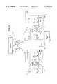
- FIG. 1is a schematic diagram of an exemplary staging buffer which may be used with high speed memory architectures
- FIG. 2is a schematic diagram of the first stage of the split sense amplifier and staging buffer in accordance with a preferred embodiment of the present invention
- FIG. 3is a schematic diagram of the second stage of the split sense amplifier and staging buffer in accordance with a preferred embodiment of the present invention
- FIG. 4is a block diagram of an N-port split sense amplifier and staging buffer which can be realized according to the teachings of the present invention.
- FIG. 5is a schematic diagram of a two-port split sense amplifier and staging buffer according to a preferred embodiment of the present invention.
- the present inventionis directed to a memory device which is capable of temporarily storing the data for multiple, simultaneously operating, vector units which form a parallel or vector process.
- staging buffersare employed as an intermediate storage cell for each data bit.
- the vector unitsread/write their intermediate results from/to dedicated staging buffers. This technique serves to eliminate the transfer of intermediate computational data across the primary data bus, and thus allows the parallel process to operate with significantly higher throughput.
- the requirement for the efficient transfer of intermediate datais an increasing concern with highly parallel vector and FFT processors.
- staging buffersin addition to all of the other circuitry, such as sense amplifiers, required to support high speed memory is not always possible because of space and power limitations of the integrated circuit. Accordingly, the sense amplifier and staging buffer design of the present invention allows these two functions to be combined, thereby providing a high speed staging buffer memory cell without increasing the power and density requirements of the memory circuit.
- staging buffer 10is disposed along each data line 16 of the data bus.
- Transistor 1connected between data line 16 and node 18, allows the transfer of data between the data bus and the staging buffer 10 and is controlled by read enable line 14.
- the staging buffer circuit 10includes a first inverter 20 an d a second inverter 22 connected end-to-end, with the output of second inverter 22 connected to the input of first inverter 20 through transistor 24, which is operated by a complementary read enable line RE 26.
- transistors 12 and 24will always be held in opposite switched states because of the complementary logic signals presented on read enable line 14 and inverse read enable line 26.
- the output of first inverter 20is fed to the input of a third inverter 30 at node 28.
- the output of third inverter 30connects to the data output line 36 through transistor 32, which is switched on and off through output enable line 34.
- This conventional staging buffer 10operates as a memory cell or latch when a particular data value is written to the staging buffer 10.
- the staging buffer 10can read and store one bit of data from data line 16 when read enable transistors 12 and 24 are simultaneously turned on and off respectively.
- the latch circuit created by invertors 20 and 22memorize the logic value from data line 16, and will remain indefinitely at the acquired logic state after read enable transistors 12 and 24 are turned off and on, respectively.
- the stored data valuecan be transferred from staging buffer 10 to the data output line 36 by switching on transistor 32 through output enable line 34.
- inverter 30 and transistor 32can be effectively replaced by an inverting tri-state buffer without changing the operation of the circuit.
- FIG. 2depicts the first stage sense amplifier 40 of a two stage sense amplifier used with the preferred implementation of the present invention.
- First stage sense amplifier 40includes a data line 42 connected to the gate of transistor 44, which has its drain connected to the appropriate true logic voltage 46, preferably 3.3V.
- a complementary data line (D) 52is connected to the gate of transistor 54.
- the drain of transistor 54is also connected to the true logic voltage source 56, preferably 3.3V.
- Data lines 42 and 52typically receive one bit of data from memory.
- An equalization transistor 48is connected between the sources of transistors 44 and 54 forming nodes 58 and 60.
- the source of transistor 44is also connected to the drain of transistor 64 and cross-connected to the gate 70 of transistor 68.
- the source of transistor 54is connected to the drain of transistor 68, which is also cross-connected to the gate 66 of transistor 64.
- the sources of transistors 64 and 68are then connected to ground 74 (logic state false).
- node 58 between transistors 44 and 64produces the sense amplified (SA) output signal line 62 which is connected to the corresponding SA signal line 62 of the second stage of the amplifier.
- node 60 between transistors 54 and 68produces the complementary sense amplified (SA) output signal line 72 which is connected to the corresponding (SA) signal line 72 of the second stage of the amplifier.
- all of the transistors disclosedare N-channel enhancement type MOSFET transistors. However, one skilled in the art will appreciate that many different types of transistors could be substituted without deviating from the scope of the present invention.
- SA signal line 62is connected to the gate of p-channel transistor 82.
- the source of transistor 82is connected to true logic node 84, preferably 3.3V, and the drain of transistor 82 is connected to p-channel read enable transistor 86.
- the drain of read enable transistor 86is connected to node 88 which is also connected to the gates of transistors 104 and 120.
- SA signal line 72is connected to the gate of p-channel transistor 92.
- the source of transistor 92is connected to true logic node 94, also preferably 3.3V, and the drain of transistor 92 is connected to the source of p-channel read enable transistor 96.
- the drain of read enable transistor 96is connected to node 90 which is commonly connected to the upper and lower gates of transistors 102 and 118, respectively.
- Node 88controls the gate of transistor 104, and node 90 controls the gate of transistor 102, thereby forming upper cross-connected transistor pair 114. Likewise, node 88 also controls the gate of transistor 120 and node 90 controls the gate of transistor 118, thereby forming lower cross-connected transistor pair 116.
- a p-channel EQ transistor 106is connected between true logic voltage node 108 and the common source connection of upper cross-connected transistors 102 and 104.
- EQ signal line 110is connected to the gate of upper EQ transistor 106.
- An n-channel EQ transistor 112is connected between DO node 88 and DO node 90. The commonly connected EQ signal line 110 is connected to the gate of lower EQ transistor 112.
- upper cross-connected transistor pair 114With respect to upper cross-connected transistor pair 114, the drain of transistor 104 is cross-connected to the gate of transistor 102, and the drain of transistor 102 is cross-connected to the gate of transistor 104.
- lower cross-connected transistor pair 116the drain of transistor 118 is cross-connected to the gate of transistor 120, and the drain of transistor 120 is cross-connected to the gate of transistor 118.
- the sources of transistors 118 and 120are connected to ground node 122.
- upper cross-connected transistor pair 114is formed using p-channel transistors (MOSFETs), and lower cross-connected transistor pair 116 is formed using n-channel transistors (MOSFETs).
- the upper and lower cross-connected pairs of transistors 114, 116effectively creates a staging buffer or memory latch for storing one bit of data. Accordingly, one skilled in the art will recognize the advantages achieved by the present invention, namely the low power consumption and the reduced number of transistors required to implement the second stage sense amplifier and staging buffer combination. Additional benefits of this improved circuit design will be discussed in more detail below.
- node 90is connected to the input of inverter 124.
- the output of inverter 124connects to the appropriate data output line 130 through output transistor 126.
- the transfer of one data bit stored in staging buffer 80 to the data output line 130is controlled by output enable line 128, connected to the gate of output enable transistor 126. While it is preferred to use an inverter 124, one skilled in the art will appreciate that inverter 124 can be replaced with a standard buffer (not shown), if the desired output logic signal needs to be the inverse of the input signal on D line 42.
- first stage sense amplifier 40is connected between a memory 38 via D line 42 and D line 52, and a common data bus 132 via SA data line 62 and SA data line 72.
- FIG. 4illustrates four staging buffers 80a through 80d, all commonly connected to common data bus 132. More importantly, however, FIG. 4 represents that N staging buffers can be connected between a memory 38 and sense amplifier 40 via common data bus 132 and the vector units 134a and 134b of a parallel or vector processor. Accordingly, the exact number of staging buffers allocated to a particular vector unit will depend upon the requirements of the vector processor.
- the memory unit 38designed to support an exemplary vector processor, is connected to a dedicated first stage sense amplifier 40.
- a block of data operandscan be transferred or pre-loaded from the memory unit 38 to a particular staging buffer via the sense amplifier 40.
- the vector processoris made up of one or more vector units 134a, 134b.
- the vector unitsare then made up of execution blocks (not shown). Because a parallel processor, such as a vector or FFT processor, is designed to perform computationally intensive algorithms, it produces many intermediate results, which are then used by subsequent execution blocks of the vector unit. In a particular application, an execution block may require two or more data operands upon which it performs a predetermined instruction or operation. An example might be multiplying two numbers.
- Datais transferred from the memory unit 38 during one or more consecutive clock cycles, through sense amplifier 40, and into the selected staging buffers 80a-80d through common data bus 132.
- the particular staging buffers identified for receiving data operands from memory 38are selected by enabling the appropriate read enable (RE) line or lines 98 through conventional memory addressing techniques. While FIG. 4 represents N staging buffers connected to a single sense amplifier 40, the actual number of staging buffers is typically optimized to the requirements of the particular vector unit.
- a vector unitrepresents functions like an arithmetic logic unit or an accumulator unit.
- vector unit 134amay read two vector operands, one each from staging buffers 80a and 80b, through data output lines 130a and 130b during a single clock cycle.
- the vector operandscan be transferred from the particular staging buffers to the vector unit 134a by enabling the appropriate write enable (WE) line or lines 128 through conventional memory addressing techniques.
- WEwrite enable
- the intermediate result produced by vector unit 134awill be transferred via vector unit output 136a to a selected staging buffer, such as staging buffer 80b, through a separate data bus (not shown).
- the conventional approach to implementing staging bufferswas to transfer the data through a two-stage sense amplifier to boost the data signal from its signal level as stored in the memory to the full swing voltage level, preferably 0V or 3.3V.
- the amplified data signalwas then transferred to a separate staging buffer at the full swing voltage level.
- the design of the present inventioneliminates the need for a separate staging buffer by combining this circuit function with the second stage of the sense amplifier.
- the designfurther allows the data signal to be transferred from the memory to the staging buffers at the memory voltage level, which is significantly less that the full swing voltage level.
- This technique of transferring the data signal at a voltage level which is lower than the full swing voltage levelfurther allows the data signal to be transferred to the staging buffers at a lower power level.
- This designalso eliminates the additional transistors and data lines required to implement separate staging buffers.
- the present inventionutilizes the efficiency of high speed staging buffers as an intermediate memory device without increasing the power requirements or capacitive loading on the integrated memory circuit.
- FIG. 5illustrates the preferred split sense amplifier and staging buffer design 140 for supporting the transfer of data operands between a memory 38 and a single vector unit 142 of a parallel processor. Additionally, it should be noted that the two staging buffers illustrated in this preferred embodiment have been optimized for the particular vector unit 142.
- Staging buffer 100ais designated as a read staging buffer memory cell
- staging buffer 100bis designated as a read/write staging buffer memory cell.
- One of the significant advantages of the present inventionis that the transfer or preloading of the vector operands from the memory unit 38 to the staging buffers 100a and 100b through sense amplifier 40 is performed at the existing signal voltage level as it is received from the memory unit 38, and not at the full swing voltage level, thus conserving power and reducing the total noise on the chip. More specifically, the vector operands are transferred from the memory unit 38 to the staging buffers 100a and 100b as follows. During the rising edge of the clock cycle, and prior to sensing the data signal by sense amplifier 40, an equalization pulse is presented on equalization lines 50 and 110a, which will equalize nodes SA and SA 62, 72 and also data nodes 88a and 90a of staging buffer 100a to the same potential.
- staging buffer 100bwill be loaded with vector operands from memory 38 through sense amplifier 40 in a similar fashion.
- staging buffers 100a or 100bat a voltage level significantly less than the conventional full swing voltage level. It should also be pointed out that the integration of a staging buffer into the second stage of the sense amplifier reduces the total number of transistors required to implement a memory storage cell, and also significantly reduces the routing complexity of the data signal lines of the integrated memory circuit.
- the vector unit 142will then read the data operand values preloaded in staging buffers 100a and 100b during a single clock cycle. This is accomplished by addressing staging buffers 100a and 100b through write enable lines 128a and 128b and transferring the vector operands to the vector unit 142 through data output lines (DO) 130a and 130b. Staging buffers 100a and 100b provide a data signal to vector unit 142 at the full swing voltage level. The vector unit 142 then performs its function on the two operands, and the intermediate result is transferred via vector unit output 144 to staging buffer 100b through a vector unit output data bus (not shown).
Landscapes
- Static Random-Access Memory (AREA)
Abstract
Description
Claims (17)
Priority Applications (1)
| Application Number | Priority Date | Filing Date | Title |
|---|---|---|---|
| US08/827,856US5991209A (en) | 1997-04-11 | 1997-04-11 | Split sense amplifier and staging buffer for wide memory architecture |
Applications Claiming Priority (1)
| Application Number | Priority Date | Filing Date | Title |
|---|---|---|---|
| US08/827,856US5991209A (en) | 1997-04-11 | 1997-04-11 | Split sense amplifier and staging buffer for wide memory architecture |
Publications (1)
| Publication Number | Publication Date |
|---|---|
| US5991209Atrue US5991209A (en) | 1999-11-23 |
Family
ID=25250346
Family Applications (1)
| Application Number | Title | Priority Date | Filing Date |
|---|---|---|---|
| US08/827,856Expired - LifetimeUS5991209A (en) | 1997-04-11 | 1997-04-11 | Split sense amplifier and staging buffer for wide memory architecture |
Country Status (1)
| Country | Link |
|---|---|
| US (1) | US5991209A (en) |
Cited By (142)
| Publication number | Priority date | Publication date | Assignee | Title |
|---|---|---|---|---|
| US6185142B1 (en)* | 1998-04-24 | 2001-02-06 | Sharp Kabushiki Kaisha | Apparatus for a semiconductor memory with independent reference voltage |
| US20030037208A1 (en)* | 2001-08-07 | 2003-02-20 | Frank Matthews | Integrated circuit memory devices having asynchronous flow-through capability |
| US7093083B1 (en) | 2001-12-18 | 2006-08-15 | Integrated Device Technology, Inc. | Integrated circuit memory devices having asynchronous flow-through capability |
| US20080219072A1 (en)* | 2006-03-31 | 2008-09-11 | Kristopher Chad Breen | Method and apparatus for a dynamic semiconductor memory with compact sense amplifier circuit |
| US8964496B2 (en) | 2013-07-26 | 2015-02-24 | Micron Technology, Inc. | Apparatuses and methods for performing compare operations using sensing circuitry |
| US8971124B1 (en) | 2013-08-08 | 2015-03-03 | Micron Technology, Inc. | Apparatuses and methods for performing logical operations using sensing circuitry |
| US9019785B2 (en) | 2013-09-19 | 2015-04-28 | Micron Technology, Inc. | Data shifting via a number of isolation devices |
| US9153305B2 (en) | 2013-08-30 | 2015-10-06 | Micron Technology, Inc. | Independently addressable memory array address spaces |
| US9158667B2 (en) | 2013-03-04 | 2015-10-13 | Micron Technology, Inc. | Apparatuses and methods for performing logical operations using sensing circuitry |
| US20160125919A1 (en)* | 2014-10-29 | 2016-05-05 | Micron Technology, Inc. | Apparatuses and methods for performing logical operations using sensing circuitry |
| US9430191B2 (en) | 2013-11-08 | 2016-08-30 | Micron Technology, Inc. | Division operations for memory |
| US9449674B2 (en) | 2014-06-05 | 2016-09-20 | Micron Technology, Inc. | Performing logical operations using sensing circuitry |
| US9449675B2 (en) | 2013-10-31 | 2016-09-20 | Micron Technology, Inc. | Apparatuses and methods for identifying an extremum value stored in an array of memory cells |
| US9455020B2 (en) | 2014-06-05 | 2016-09-27 | Micron Technology, Inc. | Apparatuses and methods for performing an exclusive or operation using sensing circuitry |
| US9496023B2 (en) | 2014-06-05 | 2016-11-15 | Micron Technology, Inc. | Comparison operations on logical representations of values in memory |
| US9583163B2 (en) | 2015-02-03 | 2017-02-28 | Micron Technology, Inc. | Loop structure for operations in memory |
| US9589602B2 (en) | 2014-09-03 | 2017-03-07 | Micron Technology, Inc. | Comparison operations in memory |
| US9659605B1 (en) | 2016-04-20 | 2017-05-23 | Micron Technology, Inc. | Apparatuses and methods for performing corner turn operations using sensing circuitry |
| US9659610B1 (en) | 2016-05-18 | 2017-05-23 | Micron Technology, Inc. | Apparatuses and methods for shifting data |
| US9697876B1 (en) | 2016-03-01 | 2017-07-04 | Micron Technology, Inc. | Vertical bit vector shift in memory |
| US9704540B2 (en) | 2014-06-05 | 2017-07-11 | Micron Technology, Inc. | Apparatuses and methods for parity determination using sensing circuitry |
| US9704541B2 (en) | 2015-06-12 | 2017-07-11 | Micron Technology, Inc. | Simulating access lines |
| US9711207B2 (en) | 2014-06-05 | 2017-07-18 | Micron Technology, Inc. | Performing logical operations using sensing circuitry |
| US9711206B2 (en) | 2014-06-05 | 2017-07-18 | Micron Technology, Inc. | Performing logical operations using sensing circuitry |
| US9740607B2 (en) | 2014-09-03 | 2017-08-22 | Micron Technology, Inc. | Swap operations in memory |
| US9741399B2 (en) | 2015-03-11 | 2017-08-22 | Micron Technology, Inc. | Data shift by elements of a vector in memory |
| US9747960B2 (en) | 2014-12-01 | 2017-08-29 | Micron Technology, Inc. | Apparatuses and methods for converting a mask to an index |
| US9747961B2 (en) | 2014-09-03 | 2017-08-29 | Micron Technology, Inc. | Division operations in memory |
| US9761300B1 (en) | 2016-11-22 | 2017-09-12 | Micron Technology, Inc. | Data shift apparatuses and methods |
| US9767864B1 (en) | 2016-07-21 | 2017-09-19 | Micron Technology, Inc. | Apparatuses and methods for storing a data value in a sensing circuitry element |
| US9779019B2 (en) | 2014-06-05 | 2017-10-03 | Micron Technology, Inc. | Data storage layout |
| US9786335B2 (en) | 2014-06-05 | 2017-10-10 | Micron Technology, Inc. | Apparatuses and methods for performing logical operations using sensing circuitry |
| US9805772B1 (en) | 2016-10-20 | 2017-10-31 | Micron Technology, Inc. | Apparatuses and methods to selectively perform logical operations |
| US9818459B2 (en) | 2016-04-19 | 2017-11-14 | Micron Technology, Inc. | Invert operations using sensing circuitry |
| US9830999B2 (en) | 2014-06-05 | 2017-11-28 | Micron Technology, Inc. | Comparison operations in memory |
| US9836218B2 (en) | 2014-10-03 | 2017-12-05 | Micron Technology, Inc. | Computing reduction and prefix sum operations in memory |
| US9847110B2 (en) | 2014-09-03 | 2017-12-19 | Micron Technology, Inc. | Apparatuses and methods for storing a data value in multiple columns of an array corresponding to digits of a vector |
| US9892767B2 (en) | 2016-02-12 | 2018-02-13 | Micron Technology, Inc. | Data gathering in memory |
| US9898253B2 (en) | 2015-03-11 | 2018-02-20 | Micron Technology, Inc. | Division operations on variable length elements in memory |
| US9898252B2 (en) | 2014-09-03 | 2018-02-20 | Micron Technology, Inc. | Multiplication operations in memory |
| US9899070B2 (en) | 2016-02-19 | 2018-02-20 | Micron Technology, Inc. | Modified decode for corner turn |
| US9905276B2 (en) | 2015-12-21 | 2018-02-27 | Micron Technology, Inc. | Control of sensing components in association with performing operations |
| US9904515B2 (en) | 2014-09-03 | 2018-02-27 | Micron Technology, Inc. | Multiplication operations in memory |
| US9910787B2 (en) | 2014-06-05 | 2018-03-06 | Micron Technology, Inc. | Virtual address table |
| US9910637B2 (en) | 2016-03-17 | 2018-03-06 | Micron Technology, Inc. | Signed division in memory |
| US9921777B2 (en) | 2015-06-22 | 2018-03-20 | Micron Technology, Inc. | Apparatuses and methods for data transfer from sensing circuitry to a controller |
| US9934856B2 (en) | 2014-03-31 | 2018-04-03 | Micron Technology, Inc. | Apparatuses and methods for comparing data patterns in memory |
| US9940026B2 (en) | 2014-10-03 | 2018-04-10 | Micron Technology, Inc. | Multidimensional contiguous memory allocation |
| US9952925B2 (en) | 2016-01-06 | 2018-04-24 | Micron Technology, Inc. | Error code calculation on sensing circuitry |
| US9959923B2 (en) | 2015-04-16 | 2018-05-01 | Micron Technology, Inc. | Apparatuses and methods to reverse data stored in memory |
| US9971541B2 (en) | 2016-02-17 | 2018-05-15 | Micron Technology, Inc. | Apparatuses and methods for data movement |
| US9972367B2 (en) | 2016-07-21 | 2018-05-15 | Micron Technology, Inc. | Shifting data in sensing circuitry |
| US9990181B2 (en) | 2016-08-03 | 2018-06-05 | Micron Technology, Inc. | Apparatuses and methods for random number generation |
| US9997212B1 (en) | 2017-04-24 | 2018-06-12 | Micron Technology, Inc. | Accessing data in memory |
| US9996479B2 (en) | 2015-08-17 | 2018-06-12 | Micron Technology, Inc. | Encryption of executables in computational memory |
| US9997232B2 (en) | 2016-03-10 | 2018-06-12 | Micron Technology, Inc. | Processing in memory (PIM) capable memory device having sensing circuitry performing logic operations |
| US10013197B1 (en) | 2017-06-01 | 2018-07-03 | Micron Technology, Inc. | Shift skip |
| US10014034B2 (en) | 2016-10-06 | 2018-07-03 | Micron Technology, Inc. | Shifting data in sensing circuitry |
| US10032493B2 (en) | 2015-01-07 | 2018-07-24 | Micron Technology, Inc. | Longest element length determination in memory |
| US10037785B2 (en) | 2016-07-08 | 2018-07-31 | Micron Technology, Inc. | Scan chain operation in sensing circuitry |
| US10043570B1 (en) | 2017-04-17 | 2018-08-07 | Micron Technology, Inc. | Signed element compare in memory |
| US10042608B2 (en) | 2016-05-11 | 2018-08-07 | Micron Technology, Inc. | Signed division in memory |
| US10048888B2 (en) | 2016-02-10 | 2018-08-14 | Micron Technology, Inc. | Apparatuses and methods for partitioned parallel data movement |
| US10049707B2 (en) | 2016-06-03 | 2018-08-14 | Micron Technology, Inc. | Shifting data |
| US10049721B1 (en) | 2017-03-27 | 2018-08-14 | Micron Technology, Inc. | Apparatuses and methods for in-memory operations |
| US10049054B2 (en) | 2015-04-01 | 2018-08-14 | Micron Technology, Inc. | Virtual register file |
| US10061590B2 (en) | 2015-01-07 | 2018-08-28 | Micron Technology, Inc. | Generating and executing a control flow |
| US10068652B2 (en) | 2014-09-03 | 2018-09-04 | Micron Technology, Inc. | Apparatuses and methods for determining population count |
| US10068664B1 (en) | 2017-05-19 | 2018-09-04 | Micron Technology, Inc. | Column repair in memory |
| US10073786B2 (en) | 2015-05-28 | 2018-09-11 | Micron Technology, Inc. | Apparatuses and methods for compute enabled cache |
| US10074407B2 (en) | 2014-06-05 | 2018-09-11 | Micron Technology, Inc. | Apparatuses and methods for performing invert operations using sensing circuitry |
| US10073635B2 (en) | 2014-12-01 | 2018-09-11 | Micron Technology, Inc. | Multiple endianness compatibility |
| US10074416B2 (en) | 2016-03-28 | 2018-09-11 | Micron Technology, Inc. | Apparatuses and methods for data movement |
| US10120740B2 (en) | 2016-03-22 | 2018-11-06 | Micron Technology, Inc. | Apparatus and methods for debugging on a memory device |
| US10140104B2 (en) | 2015-04-14 | 2018-11-27 | Micron Technology, Inc. | Target architecture determination |
| US10147480B2 (en) | 2014-10-24 | 2018-12-04 | Micron Technology, Inc. | Sort operation in memory |
| US10147467B2 (en) | 2017-04-17 | 2018-12-04 | Micron Technology, Inc. | Element value comparison in memory |
| US10146537B2 (en) | 2015-03-13 | 2018-12-04 | Micron Technology, Inc. | Vector population count determination in memory |
| US10152271B1 (en) | 2017-06-07 | 2018-12-11 | Micron Technology, Inc. | Data replication |
| US10153008B2 (en) | 2016-04-20 | 2018-12-11 | Micron Technology, Inc. | Apparatuses and methods for performing corner turn operations using sensing circuitry |
| US10162005B1 (en) | 2017-08-09 | 2018-12-25 | Micron Technology, Inc. | Scan chain operations |
| US10163467B2 (en) | 2014-10-16 | 2018-12-25 | Micron Technology, Inc. | Multiple endianness compatibility |
| US10185674B2 (en) | 2017-03-22 | 2019-01-22 | Micron Technology, Inc. | Apparatus and methods for in data path compute operations |
| US10199088B2 (en) | 2016-03-10 | 2019-02-05 | Micron Technology, Inc. | Apparatuses and methods for cache invalidate |
| US10236038B2 (en) | 2017-05-15 | 2019-03-19 | Micron Technology, Inc. | Bank to bank data transfer |
| US10262701B2 (en) | 2017-06-07 | 2019-04-16 | Micron Technology, Inc. | Data transfer between subarrays in memory |
| US10268389B2 (en) | 2017-02-22 | 2019-04-23 | Micron Technology, Inc. | Apparatuses and methods for in-memory operations |
| US10289542B2 (en) | 2015-02-06 | 2019-05-14 | Micron Technology, Inc. | Apparatuses and methods for memory device as a store for block program instructions |
| US10303632B2 (en) | 2016-07-26 | 2019-05-28 | Micron Technology, Inc. | Accessing status information |
| US10318168B2 (en) | 2017-06-19 | 2019-06-11 | Micron Technology, Inc. | Apparatuses and methods for simultaneous in data path compute operations |
| US10332586B1 (en) | 2017-12-19 | 2019-06-25 | Micron Technology, Inc. | Apparatuses and methods for subrow addressing |
| US10346092B2 (en) | 2017-08-31 | 2019-07-09 | Micron Technology, Inc. | Apparatuses and methods for in-memory operations using timing circuitry |
| US10365851B2 (en) | 2015-03-12 | 2019-07-30 | Micron Technology, Inc. | Apparatuses and methods for data movement |
| US10373666B2 (en) | 2016-11-08 | 2019-08-06 | Micron Technology, Inc. | Apparatuses and methods for compute components formed over an array of memory cells |
| US10379772B2 (en) | 2016-03-16 | 2019-08-13 | Micron Technology, Inc. | Apparatuses and methods for operations using compressed and decompressed data |
| US10387058B2 (en) | 2016-09-29 | 2019-08-20 | Micron Technology, Inc. | Apparatuses and methods to change data category values |
| US10387046B2 (en) | 2016-06-22 | 2019-08-20 | Micron Technology, Inc. | Bank to bank data transfer |
| US10388360B2 (en) | 2016-07-19 | 2019-08-20 | Micron Technology, Inc. | Utilization of data stored in an edge section of an array |
| US10388393B2 (en) | 2016-03-22 | 2019-08-20 | Micron Technology, Inc. | Apparatus and methods for debugging on a host and memory device |
| US10387299B2 (en) | 2016-07-20 | 2019-08-20 | Micron Technology, Inc. | Apparatuses and methods for transferring data |
| US10402340B2 (en) | 2017-02-21 | 2019-09-03 | Micron Technology, Inc. | Memory array page table walk |
| US10403352B2 (en) | 2017-02-22 | 2019-09-03 | Micron Technology, Inc. | Apparatuses and methods for compute in data path |
| US10409739B2 (en) | 2017-10-24 | 2019-09-10 | Micron Technology, Inc. | Command selection policy |
| US10416927B2 (en) | 2017-08-31 | 2019-09-17 | Micron Technology, Inc. | Processing in memory |
| US10423353B2 (en) | 2016-11-11 | 2019-09-24 | Micron Technology, Inc. | Apparatuses and methods for memory alignment |
| US10430244B2 (en) | 2016-03-28 | 2019-10-01 | Micron Technology, Inc. | Apparatuses and methods to determine timing of operations |
| US10437557B2 (en) | 2018-01-31 | 2019-10-08 | Micron Technology, Inc. | Determination of a match between data values stored by several arrays |
| US10440341B1 (en) | 2018-06-07 | 2019-10-08 | Micron Technology, Inc. | Image processor formed in an array of memory cells |
| US10453502B2 (en) | 2016-04-04 | 2019-10-22 | Micron Technology, Inc. | Memory bank power coordination including concurrently performing a memory operation in a selected number of memory regions |
| US10466928B2 (en) | 2016-09-15 | 2019-11-05 | Micron Technology, Inc. | Updating a register in memory |
| US10468087B2 (en) | 2016-07-28 | 2019-11-05 | Micron Technology, Inc. | Apparatuses and methods for operations in a self-refresh state |
| US10474581B2 (en) | 2016-03-25 | 2019-11-12 | Micron Technology, Inc. | Apparatuses and methods for cache operations |
| US10483978B1 (en) | 2018-10-16 | 2019-11-19 | Micron Technology, Inc. | Memory device processing |
| US10496286B2 (en) | 2015-02-06 | 2019-12-03 | Micron Technology, Inc. | Apparatuses and methods for parallel writing to multiple memory device structures |
| US10522210B2 (en) | 2017-12-14 | 2019-12-31 | Micron Technology, Inc. | Apparatuses and methods for subarray addressing |
| US10522199B2 (en) | 2015-02-06 | 2019-12-31 | Micron Technology, Inc. | Apparatuses and methods for scatter and gather |
| US10522212B2 (en) | 2015-03-10 | 2019-12-31 | Micron Technology, Inc. | Apparatuses and methods for shift decisions |
| US10529409B2 (en) | 2016-10-13 | 2020-01-07 | Micron Technology, Inc. | Apparatuses and methods to perform logical operations using sensing circuitry |
| US10534553B2 (en) | 2017-08-30 | 2020-01-14 | Micron Technology, Inc. | Memory array accessibility |
| US10607665B2 (en) | 2016-04-07 | 2020-03-31 | Micron Technology, Inc. | Span mask generation |
| US10606587B2 (en) | 2016-08-24 | 2020-03-31 | Micron Technology, Inc. | Apparatus and methods related to microcode instructions indicating instruction types |
| US10614875B2 (en) | 2018-01-30 | 2020-04-07 | Micron Technology, Inc. | Logical operations using memory cells |
| US10725696B2 (en) | 2018-04-12 | 2020-07-28 | Micron Technology, Inc. | Command selection policy with read priority |
| US10733089B2 (en) | 2016-07-20 | 2020-08-04 | Micron Technology, Inc. | Apparatuses and methods for write address tracking |
| US10741239B2 (en) | 2017-08-31 | 2020-08-11 | Micron Technology, Inc. | Processing in memory device including a row address strobe manager |
| US10838899B2 (en) | 2017-03-21 | 2020-11-17 | Micron Technology, Inc. | Apparatuses and methods for in-memory data switching networks |
| US10942843B2 (en) | 2017-04-25 | 2021-03-09 | Micron Technology, Inc. | Storing data elements of different lengths in respective adjacent rows or columns according to memory shapes |
| US10956439B2 (en) | 2016-02-19 | 2021-03-23 | Micron Technology, Inc. | Data transfer with a bit vector operation device |
| US10977033B2 (en) | 2016-03-25 | 2021-04-13 | Micron Technology, Inc. | Mask patterns generated in memory from seed vectors |
| US11029951B2 (en) | 2016-08-15 | 2021-06-08 | Micron Technology, Inc. | Smallest or largest value element determination |
| US11074988B2 (en) | 2016-03-22 | 2021-07-27 | Micron Technology, Inc. | Apparatus and methods for debugging on a host and memory device |
| US11175915B2 (en) | 2018-10-10 | 2021-11-16 | Micron Technology, Inc. | Vector registers implemented in memory |
| US11184446B2 (en) | 2018-12-05 | 2021-11-23 | Micron Technology, Inc. | Methods and apparatus for incentivizing participation in fog networks |
| US11194477B2 (en) | 2018-01-31 | 2021-12-07 | Micron Technology, Inc. | Determination of a match between data values stored by three or more arrays |
| US11222260B2 (en) | 2017-03-22 | 2022-01-11 | Micron Technology, Inc. | Apparatuses and methods for operating neural networks |
| US11227641B1 (en) | 2020-07-21 | 2022-01-18 | Micron Technology, Inc. | Arithmetic operations in memory |
| US11360768B2 (en) | 2019-08-14 | 2022-06-14 | Micron Technolgy, Inc. | Bit string operations in memory |
| US11398264B2 (en) | 2019-07-08 | 2022-07-26 | Micron Technology, Inc. | Methods and apparatus for dynamically adjusting performance of partitioned memory |
| US11397688B2 (en) | 2018-10-10 | 2022-07-26 | Micron Technology, Inc. | Coherent memory access |
| US11449577B2 (en) | 2019-11-20 | 2022-09-20 | Micron Technology, Inc. | Methods and apparatus for performing video processing matrix operations within a memory array |
| US11853385B2 (en) | 2019-12-05 | 2023-12-26 | Micron Technology, Inc. | Methods and apparatus for performing diversity matrix operations within a memory array |
| US12118056B2 (en) | 2019-05-03 | 2024-10-15 | Micron Technology, Inc. | Methods and apparatus for performing matrix transformations within a memory array |
Citations (6)
| Publication number | Priority date | Publication date | Assignee | Title |
|---|---|---|---|---|
| US5311469A (en)* | 1991-03-04 | 1994-05-10 | Kabushiki Kaisha Toshiba | Semiconductor memory device |
| US5311471A (en)* | 1989-11-27 | 1994-05-10 | Kabushiki Kaisha Toshiba | Semiconductor memory device |
| US5341341A (en)* | 1992-03-26 | 1994-08-23 | Nec Corporation | Dynamic random access memory device having addressing section and/or data transferring path arranged in pipeline architecture |
| US5418737A (en)* | 1990-09-17 | 1995-05-23 | Texas Instruments Incorporated | DRAM with sub data lines and match lines for test |
| US5537352A (en)* | 1992-07-24 | 1996-07-16 | Siemens Aktiengesellschaft | Integrated semiconductor memory configuration |
| US5726943A (en)* | 1995-01-06 | 1998-03-10 | Mitsubishi Denki Kabushiki Kaisha | Fast memory device allowing suppression of peak value of operational current |
- 1997
- 1997-04-11USUS08/827,856patent/US5991209A/ennot_activeExpired - Lifetime
Patent Citations (6)
| Publication number | Priority date | Publication date | Assignee | Title |
|---|---|---|---|---|
| US5311471A (en)* | 1989-11-27 | 1994-05-10 | Kabushiki Kaisha Toshiba | Semiconductor memory device |
| US5418737A (en)* | 1990-09-17 | 1995-05-23 | Texas Instruments Incorporated | DRAM with sub data lines and match lines for test |
| US5311469A (en)* | 1991-03-04 | 1994-05-10 | Kabushiki Kaisha Toshiba | Semiconductor memory device |
| US5341341A (en)* | 1992-03-26 | 1994-08-23 | Nec Corporation | Dynamic random access memory device having addressing section and/or data transferring path arranged in pipeline architecture |
| US5537352A (en)* | 1992-07-24 | 1996-07-16 | Siemens Aktiengesellschaft | Integrated semiconductor memory configuration |
| US5726943A (en)* | 1995-01-06 | 1998-03-10 | Mitsubishi Denki Kabushiki Kaisha | Fast memory device allowing suppression of peak value of operational current |
Cited By (417)
| Publication number | Priority date | Publication date | Assignee | Title |
|---|---|---|---|---|
| US6185142B1 (en)* | 1998-04-24 | 2001-02-06 | Sharp Kabushiki Kaisha | Apparatus for a semiconductor memory with independent reference voltage |
| US20030037208A1 (en)* | 2001-08-07 | 2003-02-20 | Frank Matthews | Integrated circuit memory devices having asynchronous flow-through capability |
| US6934816B2 (en) | 2001-08-07 | 2005-08-23 | Integrated Device Technology, Inc. | Integrated circuit memory devices having asynchronous flow-through capability |
| US7093083B1 (en) | 2001-12-18 | 2006-08-15 | Integrated Device Technology, Inc. | Integrated circuit memory devices having asynchronous flow-through capability |
| US20080219072A1 (en)* | 2006-03-31 | 2008-09-11 | Kristopher Chad Breen | Method and apparatus for a dynamic semiconductor memory with compact sense amplifier circuit |
| US8027212B2 (en)* | 2006-03-31 | 2011-09-27 | Kristopher Chad Breen | Method and apparatus for a dynamic semiconductor memory with compact sense amplifier circuit |
| US11276439B2 (en) | 2013-03-04 | 2022-03-15 | Micron Technology, Inc. | Apparatuses and methods for performing logical operations using sensing circuitry |
| US9892766B2 (en) | 2013-03-04 | 2018-02-13 | Micron Technology, Inc. | Apparatuses and methods for performing logical operations using sensing circuitry |
| US10796733B2 (en) | 2013-03-04 | 2020-10-06 | Micron Technology, Inc. | Apparatuses and methods for performing logical operations using sensing circuitry |
| US9959913B2 (en) | 2013-03-04 | 2018-05-01 | Micron Technology, Inc. | Apparatuses and methods for performing logical operations using sensing circuitry |
| US9158667B2 (en) | 2013-03-04 | 2015-10-13 | Micron Technology, Inc. | Apparatuses and methods for performing logical operations using sensing circuitry |
| US11727963B2 (en) | 2013-03-04 | 2023-08-15 | Micron Technology, Inc. | Apparatuses and methods for performing logical operations using sensing circuitry |
| US10153009B2 (en) | 2013-03-04 | 2018-12-11 | Micron Technology, Inc. | Apparatuses and methods for performing logical operations using sensing circuitry |
| US10431264B2 (en) | 2013-03-04 | 2019-10-01 | Micron Technology, Inc. | Apparatuses and methods for performing logical operations using sensing circuitry |
| US9472265B2 (en) | 2013-03-04 | 2016-10-18 | Micron Technology, Inc. | Apparatuses and methods for performing logical operations using sensing circuitry |
| US10056122B2 (en) | 2013-07-26 | 2018-08-21 | Micron Technology, Inc. | Apparatuses and methods for performing compare operations using sensing circuitry |
| US9799378B2 (en) | 2013-07-26 | 2017-10-24 | Micron Technology, Inc. | Apparatuses and methods for performing compare operations using sensing circuitry |
| US8964496B2 (en) | 2013-07-26 | 2015-02-24 | Micron Technology, Inc. | Apparatuses and methods for performing compare operations using sensing circuitry |
| US9466340B2 (en) | 2013-07-26 | 2016-10-11 | Micron Technology, Inc. | Apparatuses and methods for performing compare operations using sensing circuitry |
| US10643673B2 (en) | 2013-07-26 | 2020-05-05 | Micron Technology, Inc. | Apparatuses and methods for performing compare operations using sensing circuitry |
| US10535384B2 (en) | 2013-08-08 | 2020-01-14 | Micron Technology, Inc. | Apparatuses and methods for performing logical operations using sensing circuitry |
| US12142347B2 (en) | 2013-08-08 | 2024-11-12 | Lodestar Licensing Group Llc | Apparatuses and methods for performing logical operations using sensing circuitry |
| US10186303B2 (en) | 2013-08-08 | 2019-01-22 | Micron Technology, Inc. | Apparatuses and methods for performing logical operations using sensing circuitry |
| US9589607B2 (en) | 2013-08-08 | 2017-03-07 | Micron Technology, Inc. | Apparatuses and methods for performing logical operations using sensing circuitry |
| US8971124B1 (en) | 2013-08-08 | 2015-03-03 | Micron Technology, Inc. | Apparatuses and methods for performing logical operations using sensing circuitry |
| US9899068B2 (en) | 2013-08-08 | 2018-02-20 | Micron Technology, Inc. | Apparatuses and methods for performing logical operations using sensing circuitry |
| US9275701B2 (en) | 2013-08-08 | 2016-03-01 | Micron Technology, Inc. | Apparatuses and methods for performing logical operations using sensing circuitry |
| US10878863B2 (en) | 2013-08-08 | 2020-12-29 | Micron Technology, Inc. | Apparatuses and methods for performing logical operations using sensing circuitry |
| US11495274B2 (en) | 2013-08-08 | 2022-11-08 | Micron Technology, Inc. | Apparatuses and methods for performing logical operations using sensing circuitry |
| US9153305B2 (en) | 2013-08-30 | 2015-10-06 | Micron Technology, Inc. | Independently addressable memory array address spaces |
| US9530475B2 (en) | 2013-08-30 | 2016-12-27 | Micron Technology, Inc. | Independently addressable memory array address spaces |
| US9019785B2 (en) | 2013-09-19 | 2015-04-28 | Micron Technology, Inc. | Data shifting via a number of isolation devices |
| US9437256B2 (en) | 2013-09-19 | 2016-09-06 | Micron Technology, Inc. | Data shifting |
| US10043556B2 (en) | 2013-09-19 | 2018-08-07 | Micron Technology, Inc. | Data shifting |
| US9830955B2 (en) | 2013-09-19 | 2017-11-28 | Micron Technology, Inc. | Data shifting |
| US9449675B2 (en) | 2013-10-31 | 2016-09-20 | Micron Technology, Inc. | Apparatuses and methods for identifying an extremum value stored in an array of memory cells |
| US10579336B2 (en) | 2013-11-08 | 2020-03-03 | Micron Technology, Inc. | Division operations for memory |
| US9430191B2 (en) | 2013-11-08 | 2016-08-30 | Micron Technology, Inc. | Division operations for memory |
| US10055196B2 (en) | 2013-11-08 | 2018-08-21 | Micron Technology, Inc. | Division operations for memory |
| US10726919B2 (en) | 2014-03-31 | 2020-07-28 | Micron Technology, Inc. | Apparatuses and methods for comparing data patterns in memory |
| US9934856B2 (en) | 2014-03-31 | 2018-04-03 | Micron Technology, Inc. | Apparatuses and methods for comparing data patterns in memory |
| US11393531B2 (en) | 2014-03-31 | 2022-07-19 | Micron Technology, Inc. | Apparatuses and methods for comparing data patterns in memory |
| US10522211B2 (en) | 2014-06-05 | 2019-12-31 | Micron Technology, Inc. | Performing logical operations using sensing circuitry |
| US10593418B2 (en) | 2014-06-05 | 2020-03-17 | Micron Technology, Inc. | Comparison operations in memory |
| US11238920B2 (en) | 2014-06-05 | 2022-02-01 | Micron Technology, Inc. | Comparison operations in memory |
| US11205497B2 (en) | 2014-06-05 | 2021-12-21 | Micron Technology, Inc. | Comparison operations in memory |
| US9830999B2 (en) | 2014-06-05 | 2017-11-28 | Micron Technology, Inc. | Comparison operations in memory |
| US9779019B2 (en) | 2014-06-05 | 2017-10-03 | Micron Technology, Inc. | Data storage layout |
| US12437801B2 (en) | 2014-06-05 | 2025-10-07 | Lodestar Licensing Group Llc | Comparison operations in memory |
| US10090041B2 (en) | 2014-06-05 | 2018-10-02 | Micro Technology, Inc. | Performing logical operations using sensing circuitry |
| US11120850B2 (en) | 2014-06-05 | 2021-09-14 | Micron Technology, Inc. | Performing logical operations using sensing circuitry |
| US9449674B2 (en) | 2014-06-05 | 2016-09-20 | Micron Technology, Inc. | Performing logical operations using sensing circuitry |
| US9455020B2 (en) | 2014-06-05 | 2016-09-27 | Micron Technology, Inc. | Apparatuses and methods for performing an exclusive or operation using sensing circuitry |
| US10074407B2 (en) | 2014-06-05 | 2018-09-11 | Micron Technology, Inc. | Apparatuses and methods for performing invert operations using sensing circuitry |
| US10210911B2 (en) | 2014-06-05 | 2019-02-19 | Micron Technology, Inc. | Apparatuses and methods for performing logical operations using sensing circuitry in a memory device |
| US10249350B2 (en) | 2014-06-05 | 2019-04-02 | Micron Technology, Inc. | Apparatuses and methods for parity determination using sensing circuitry |
| US11355178B2 (en) | 2014-06-05 | 2022-06-07 | Micron Technology, Inc. | Apparatuses and methods for performing an exclusive or operation using sensing circuitry |
| US10255193B2 (en) | 2014-06-05 | 2019-04-09 | Micron Technology, Inc. | Virtual address table |
| US9496023B2 (en) | 2014-06-05 | 2016-11-15 | Micron Technology, Inc. | Comparison operations on logical representations of values in memory |
| US9910787B2 (en) | 2014-06-05 | 2018-03-06 | Micron Technology, Inc. | Virtual address table |
| US10839892B2 (en) | 2014-06-05 | 2020-11-17 | Micron Technology, Inc. | Comparison operations in memory |
| US10839867B2 (en) | 2014-06-05 | 2020-11-17 | Micron Technology, Inc. | Apparatuses and methods for parity determination using sensing circuitry |
| US10290344B2 (en) | 2014-06-05 | 2019-05-14 | Micron Technology, Inc. | Performing logical operations using sensing circuitry |
| US11422933B2 (en) | 2014-06-05 | 2022-08-23 | Micron Technology, Inc. | Data storage layout |
| US10754787B2 (en) | 2014-06-05 | 2020-08-25 | Micron Technology, Inc. | Virtual address table |
| US10304519B2 (en) | 2014-06-05 | 2019-05-28 | Micron Technology, Inc. | Apparatuses and methods for performing an exclusive or operation using sensing circuitry |
| US10360147B2 (en) | 2014-06-05 | 2019-07-23 | Micron Technology, Inc. | Data storage layout |
| US10381065B2 (en) | 2014-06-05 | 2019-08-13 | Micron Technology, Inc. | Performing logical operations using sensing circuitry |
| US10734038B2 (en) | 2014-06-05 | 2020-08-04 | Micron Technology, Inc. | Apparatuses and methods for performing logical operations using sensing circuitry |
| US9741427B2 (en) | 2014-06-05 | 2017-08-22 | Micron Technology, Inc. | Performing logical operations using sensing circuitry |
| US11967361B2 (en) | 2014-06-05 | 2024-04-23 | Micron Technology, Inc. | Comparison operations in memory |
| US10424350B2 (en) | 2014-06-05 | 2019-09-24 | Micron Technology, Inc. | Performing logical operations using sensing circuitry |
| US10453499B2 (en) | 2014-06-05 | 2019-10-22 | Micron Technology, Inc. | Apparatuses and methods for performing an in-place inversion using sensing circuitry |
| US10490257B2 (en) | 2014-06-05 | 2019-11-26 | Micron Technology, Inc. | Comparison operations in memory |
| US9711206B2 (en) | 2014-06-05 | 2017-07-18 | Micron Technology, Inc. | Performing logical operations using sensing circuitry |
| US9786335B2 (en) | 2014-06-05 | 2017-10-10 | Micron Technology, Inc. | Apparatuses and methods for performing logical operations using sensing circuitry |
| US9704540B2 (en) | 2014-06-05 | 2017-07-11 | Micron Technology, Inc. | Apparatuses and methods for parity determination using sensing circuitry |
| US9711207B2 (en) | 2014-06-05 | 2017-07-18 | Micron Technology, Inc. | Performing logical operations using sensing circuitry |
| US10713011B2 (en) | 2014-09-03 | 2020-07-14 | Micron Technology, Inc. | Multiplication operations in memory |
| US9740607B2 (en) | 2014-09-03 | 2017-08-22 | Micron Technology, Inc. | Swap operations in memory |
| US9847110B2 (en) | 2014-09-03 | 2017-12-19 | Micron Technology, Inc. | Apparatuses and methods for storing a data value in multiple columns of an array corresponding to digits of a vector |
| US9779789B2 (en) | 2014-09-03 | 2017-10-03 | Micron Technology, Inc. | Comparison operations in memory |
| US9898252B2 (en) | 2014-09-03 | 2018-02-20 | Micron Technology, Inc. | Multiplication operations in memory |
| US10705798B2 (en) | 2014-09-03 | 2020-07-07 | Micron Technology, Inc. | Multiplication operations in memory |
| US10032491B2 (en) | 2014-09-03 | 2018-07-24 | Micron Technology, Inc. | Apparatuses and methods for storing a data value in multiple columns |
| US10559360B2 (en) | 2014-09-03 | 2020-02-11 | Micron Technology, Inc. | Apparatuses and methods for determining population count |
| US10157126B2 (en) | 2014-09-03 | 2018-12-18 | Micron Technology, Inc. | Swap operations in memory |
| US9904515B2 (en) | 2014-09-03 | 2018-02-27 | Micron Technology, Inc. | Multiplication operations in memory |
| US10409555B2 (en) | 2014-09-03 | 2019-09-10 | Micron Technology, Inc. | Multiplication operations in memory |
| US10409554B2 (en) | 2014-09-03 | 2019-09-10 | Micron Technology, Inc. | Multiplication operations in memory |
| US10068652B2 (en) | 2014-09-03 | 2018-09-04 | Micron Technology, Inc. | Apparatuses and methods for determining population count |
| US9940981B2 (en) | 2014-09-03 | 2018-04-10 | Micron Technology, Inc. | Division operations in memory |
| US9940985B2 (en) | 2014-09-03 | 2018-04-10 | Micron Technology, Inc. | Comparison operations in memory |
| US9747961B2 (en) | 2014-09-03 | 2017-08-29 | Micron Technology, Inc. | Division operations in memory |
| US10861563B2 (en) | 2014-09-03 | 2020-12-08 | Micron Technology, Inc. | Apparatuses and methods for determining population count |
| US9589602B2 (en) | 2014-09-03 | 2017-03-07 | Micron Technology, Inc. | Comparison operations in memory |
| US11768600B2 (en) | 2014-10-03 | 2023-09-26 | Micron Technology, Inc. | Computing reduction and prefix sum operations in memory |
| US10261691B2 (en) | 2014-10-03 | 2019-04-16 | Micron Technology, Inc. | Computing reduction and prefix sum operations in memory |
| US9940026B2 (en) | 2014-10-03 | 2018-04-10 | Micron Technology, Inc. | Multidimensional contiguous memory allocation |
| US10956043B2 (en) | 2014-10-03 | 2021-03-23 | Micron Technology, Inc. | Computing reduction and prefix sum operations in memory |
| US10540093B2 (en) | 2014-10-03 | 2020-01-21 | Micron Technology, Inc. | Multidimensional contiguous memory allocation |
| US9836218B2 (en) | 2014-10-03 | 2017-12-05 | Micron Technology, Inc. | Computing reduction and prefix sum operations in memory |
| US10984842B2 (en) | 2014-10-16 | 2021-04-20 | Micron Technology, Inc. | Multiple endianness compatibility |
| US10163467B2 (en) | 2014-10-16 | 2018-12-25 | Micron Technology, Inc. | Multiple endianness compatibility |
| US10593377B2 (en) | 2014-10-16 | 2020-03-17 | Micron Technology, Inc. | Multiple endianness compatibility |
| US11315626B2 (en) | 2014-10-24 | 2022-04-26 | Micron Technology, Inc. | Sort operation in memory |
| US10685699B2 (en) | 2014-10-24 | 2020-06-16 | Micron Technology, Inc. | Sort operation in memory |
| US10147480B2 (en) | 2014-10-24 | 2018-12-04 | Micron Technology, Inc. | Sort operation in memory |
| US10074406B2 (en) | 2014-10-29 | 2018-09-11 | Micron Technology, Inc. | Apparatuses and methods for performing logical operations using sensing circuitry |
| US10529387B2 (en) | 2014-10-29 | 2020-01-07 | Micron Technology, Inc. | Apparatuses and methods for performing logical operations using sensing circuitry |
| US20160125919A1 (en)* | 2014-10-29 | 2016-05-05 | Micron Technology, Inc. | Apparatuses and methods for performing logical operations using sensing circuitry |
| US9779784B2 (en)* | 2014-10-29 | 2017-10-03 | Micron Technology, Inc. | Apparatuses and methods for performing logical operations using sensing circuitry |
| US10037786B2 (en) | 2014-12-01 | 2018-07-31 | Micron Technology, Inc. | Apparatuses and methods for converting a mask to an index |
| US10460773B2 (en) | 2014-12-01 | 2019-10-29 | Micron Technology, Inc. | Apparatuses and methods for converting a mask to an index |
| US10387055B2 (en) | 2014-12-01 | 2019-08-20 | Micron Technology, Inc. | Multiple endianness compatibility |
| US9747960B2 (en) | 2014-12-01 | 2017-08-29 | Micron Technology, Inc. | Apparatuses and methods for converting a mask to an index |
| US10983706B2 (en) | 2014-12-01 | 2021-04-20 | Micron Technology, Inc. | Multiple endianness compatibility |
| US10073635B2 (en) | 2014-12-01 | 2018-09-11 | Micron Technology, Inc. | Multiple endianness compatibility |
| US10984841B2 (en) | 2015-01-07 | 2021-04-20 | Micron Technology, Inc. | Longest element length determination in memory |
| US10032493B2 (en) | 2015-01-07 | 2018-07-24 | Micron Technology, Inc. | Longest element length determination in memory |
| US10782980B2 (en) | 2015-01-07 | 2020-09-22 | Micron Technology, Inc. | Generating and executing a control flow |
| US10593376B2 (en) | 2015-01-07 | 2020-03-17 | Micron Technology, Inc. | Longest element length determination in memory |
| US11726791B2 (en) | 2015-01-07 | 2023-08-15 | Micron Technology, Inc. | Generating and executing a control flow |
| US12223328B2 (en) | 2015-01-07 | 2025-02-11 | Lodestar Licensing Group, Llc | Generating and executing a control flow |
| US11334362B2 (en) | 2015-01-07 | 2022-05-17 | Micron Technology, Inc. | Generating and executing a control flow |
| US10061590B2 (en) | 2015-01-07 | 2018-08-28 | Micron Technology, Inc. | Generating and executing a control flow |
| US9583163B2 (en) | 2015-02-03 | 2017-02-28 | Micron Technology, Inc. | Loop structure for operations in memory |
| US10176851B2 (en) | 2015-02-03 | 2019-01-08 | Micron Technology, Inc. | Loop structure for operations in memory |
| US10496286B2 (en) | 2015-02-06 | 2019-12-03 | Micron Technology, Inc. | Apparatuses and methods for parallel writing to multiple memory device structures |
| US10964358B2 (en) | 2015-02-06 | 2021-03-30 | Micron Technology, Inc. | Apparatuses and methods for scatter and gather |
| US11482260B2 (en) | 2015-02-06 | 2022-10-25 | Micron Technology, Inc. | Apparatuses and methods for scatter and gather |
| US10817414B2 (en) | 2015-02-06 | 2020-10-27 | Micron Technology, Inc. | Apparatuses and methods for memory device as a store for block program instructions |
| US10942652B2 (en) | 2015-02-06 | 2021-03-09 | Micron Technology, Inc. | Apparatuses and methods for parallel writing to multiple memory device structures |
| US10522199B2 (en) | 2015-02-06 | 2019-12-31 | Micron Technology, Inc. | Apparatuses and methods for scatter and gather |
| US12230354B2 (en) | 2015-02-06 | 2025-02-18 | Lodestar Licensing Group Llc | Apparatuses and methods for scatter and gather |
| US11263123B2 (en) | 2015-02-06 | 2022-03-01 | Micron Technology, Inc. | Apparatuses and methods for memory device as a store for program instructions |
| US10289542B2 (en) | 2015-02-06 | 2019-05-14 | Micron Technology, Inc. | Apparatuses and methods for memory device as a store for block program instructions |
| US12393342B2 (en) | 2015-02-06 | 2025-08-19 | Lodestar Licensing Group Llc | Apparatuses and methods for parallel writing to multiple memory device structures |
| US11681440B2 (en) | 2015-02-06 | 2023-06-20 | Micron Technology, Inc. | Apparatuses and methods for parallel writing to multiple memory device structures |
| US10522212B2 (en) | 2015-03-10 | 2019-12-31 | Micron Technology, Inc. | Apparatuses and methods for shift decisions |
| US11107520B2 (en) | 2015-03-10 | 2021-08-31 | Micron Technology, Inc. | Apparatuses and methods for shift decisions |
| US9928887B2 (en) | 2015-03-11 | 2018-03-27 | Micron Technology, Inc. | Data shift by elements of a vector in memory |
| US9898253B2 (en) | 2015-03-11 | 2018-02-20 | Micron Technology, Inc. | Division operations on variable length elements in memory |
| US9741399B2 (en) | 2015-03-11 | 2017-08-22 | Micron Technology, Inc. | Data shift by elements of a vector in memory |
| US10365851B2 (en) | 2015-03-12 | 2019-07-30 | Micron Technology, Inc. | Apparatuses and methods for data movement |
| US11614877B2 (en) | 2015-03-12 | 2023-03-28 | Micron Technology, Inc. | Apparatuses and methods for data movement |
| US10936235B2 (en) | 2015-03-12 | 2021-03-02 | Micron Technology, Inc. | Apparatuses and methods for data movement |
| US12242848B2 (en) | 2015-03-13 | 2025-03-04 | Lodestar Licensing Group Llc | Vector population count determination via comparison iterations in memory |
| US10146537B2 (en) | 2015-03-13 | 2018-12-04 | Micron Technology, Inc. | Vector population count determination in memory |
| US10896042B2 (en) | 2015-03-13 | 2021-01-19 | Micron Technology, Inc. | Vector population count determination via comparison iterations in memory |
| US11663005B2 (en) | 2015-03-13 | 2023-05-30 | Micron Technology, Inc. | Vector population count determination via comparsion iterations in memory |
| US10963398B2 (en) | 2015-04-01 | 2021-03-30 | Micron Technology, Inc. | Virtual register file |
| US10049054B2 (en) | 2015-04-01 | 2018-08-14 | Micron Technology, Inc. | Virtual register file |
| US11237808B2 (en) | 2015-04-14 | 2022-02-01 | Micron Technology, Inc. | Target architecture determination |
| US10140104B2 (en) | 2015-04-14 | 2018-11-27 | Micron Technology, Inc. | Target architecture determination |
| US10795653B2 (en) | 2015-04-14 | 2020-10-06 | Micron Technology, Inc. | Target architecture determination |
| US11782688B2 (en) | 2015-04-14 | 2023-10-10 | Micron Technology, Inc. | Target architecture determination |
| US10418092B2 (en) | 2015-04-16 | 2019-09-17 | Micron Technology, Inc. | Apparatuses and methods to reverse data stored in memory |
| US10878884B2 (en) | 2015-04-16 | 2020-12-29 | Micron Technology, Inc. | Apparatuses and methods to reverse data stored in memory |
| US9959923B2 (en) | 2015-04-16 | 2018-05-01 | Micron Technology, Inc. | Apparatuses and methods to reverse data stored in memory |
| US12050536B2 (en) | 2015-05-28 | 2024-07-30 | Lodestar Licensing Group Llc | Apparatuses and methods for compute enabled cache |
| US11599475B2 (en) | 2015-05-28 | 2023-03-07 | Micron Technology, Inc. | Apparatuses and methods for compute enabled cache |
| US10073786B2 (en) | 2015-05-28 | 2018-09-11 | Micron Technology, Inc. | Apparatuses and methods for compute enabled cache |
| US10372612B2 (en) | 2015-05-28 | 2019-08-06 | Micron Technology, Inc. | Apparatuses and methods for compute enabled cache |
| US10970218B2 (en) | 2015-05-28 | 2021-04-06 | Micron Technology, Inc. | Apparatuses and methods for compute enabled cache |
| US9990966B2 (en) | 2015-06-12 | 2018-06-05 | Micron Technology, Inc. | Simulating access lines |
| US9704541B2 (en) | 2015-06-12 | 2017-07-11 | Micron Technology, Inc. | Simulating access lines |
| US10431263B2 (en) | 2015-06-12 | 2019-10-01 | Micron Technology, Inc. | Simulating access lines |
| US9921777B2 (en) | 2015-06-22 | 2018-03-20 | Micron Technology, Inc. | Apparatuses and methods for data transfer from sensing circuitry to a controller |
| US11106389B2 (en) | 2015-06-22 | 2021-08-31 | Micron Technology, Inc. | Apparatuses and methods for data transfer from sensing circuitry to a controller |
| US10157019B2 (en) | 2015-06-22 | 2018-12-18 | Micron Technology, Inc. | Apparatuses and methods for data transfer from sensing circuitry to a controller |
| US9996479B2 (en) | 2015-08-17 | 2018-06-12 | Micron Technology, Inc. | Encryption of executables in computational memory |
| US10691620B2 (en) | 2015-08-17 | 2020-06-23 | Micron Technology, Inc. | Encryption of executables in computational memory |
| US11625336B2 (en) | 2015-08-17 | 2023-04-11 | Micron Technology, Inc. | Encryption of executables in computational memory |
| US10236037B2 (en) | 2015-12-21 | 2019-03-19 | Micron Technology, Inc. | Data transfer in sensing components |
| US9905276B2 (en) | 2015-12-21 | 2018-02-27 | Micron Technology, Inc. | Control of sensing components in association with performing operations |
| US10949299B2 (en) | 2016-01-06 | 2021-03-16 | Micron Technology, Inc. | Error code calculation on sensing circuitry |
| US11593200B2 (en) | 2016-01-06 | 2023-02-28 | Micron Technology, Inc. | Error code calculation on sensing circuitry |
| US9952925B2 (en) | 2016-01-06 | 2018-04-24 | Micron Technology, Inc. | Error code calculation on sensing circuitry |
| US11340983B2 (en) | 2016-01-06 | 2022-05-24 | Micron Technology, Inc. | Error code calculation on sensing circuitry |
| US10423486B2 (en) | 2016-01-06 | 2019-09-24 | Micron Technology, Inc. | Error code calculation on sensing circuitry |
| US10152374B2 (en) | 2016-01-06 | 2018-12-11 | Micron Technology, Inc. | Error code calculation on sensing circuitry |
| US10915263B2 (en) | 2016-02-10 | 2021-02-09 | Micron Technology, Inc. | Apparatuses and methods for partitioned parallel data movement |
| US11513713B2 (en) | 2016-02-10 | 2022-11-29 | Micron Technology, Inc. | Apparatuses and methods for partitioned parallel data movement |
| US10324654B2 (en) | 2016-02-10 | 2019-06-18 | Micron Technology, Inc. | Apparatuses and methods for partitioned parallel data movement |
| US10048888B2 (en) | 2016-02-10 | 2018-08-14 | Micron Technology, Inc. | Apparatuses and methods for partitioned parallel data movement |
| US9892767B2 (en) | 2016-02-12 | 2018-02-13 | Micron Technology, Inc. | Data gathering in memory |
| US10026459B2 (en) | 2016-02-12 | 2018-07-17 | Micron Technology, Inc. | Data gathering in memory |
| US11010085B2 (en) | 2016-02-17 | 2021-05-18 | Micron Technology, Inc. | Apparatuses and methods for data movement |
| US9971541B2 (en) | 2016-02-17 | 2018-05-15 | Micron Technology, Inc. | Apparatuses and methods for data movement |
| US11614878B2 (en) | 2016-02-17 | 2023-03-28 | Micron Technology, Inc. | Apparatuses and methods for data movement |
| US10353618B2 (en) | 2016-02-17 | 2019-07-16 | Micron Technology, Inc. | Apparatuses and methods for data movement |
| US12019895B2 (en) | 2016-02-17 | 2024-06-25 | Lodestar Licensing Group Llc | Apparatuses and methods for data movement |
| US10783942B2 (en) | 2016-02-19 | 2020-09-22 | Micron Technology, Inc. | Modified decode for corner turn |
| US10217499B2 (en) | 2016-02-19 | 2019-02-26 | Micron Technology, Inc. | Modified decode for corner turn |
| US11816123B2 (en) | 2016-02-19 | 2023-11-14 | Micron Technology, Inc. | Data transfer with a bit vector operation device |
| US10956439B2 (en) | 2016-02-19 | 2021-03-23 | Micron Technology, Inc. | Data transfer with a bit vector operation device |
| US12259903B2 (en) | 2016-02-19 | 2025-03-25 | Lodestar Licensing Group Llc | Data transfer with a bit vector operation device |
| US9899070B2 (en) | 2016-02-19 | 2018-02-20 | Micron Technology, Inc. | Modified decode for corner turn |
| US9697876B1 (en) | 2016-03-01 | 2017-07-04 | Micron Technology, Inc. | Vertical bit vector shift in memory |
| US9947376B2 (en) | 2016-03-01 | 2018-04-17 | Micron Technology, Inc. | Vertical bit vector shift in memory |
| US9997232B2 (en) | 2016-03-10 | 2018-06-12 | Micron Technology, Inc. | Processing in memory (PIM) capable memory device having sensing circuitry performing logic operations |
| US10199088B2 (en) | 2016-03-10 | 2019-02-05 | Micron Technology, Inc. | Apparatuses and methods for cache invalidate |
| US10878883B2 (en) | 2016-03-10 | 2020-12-29 | Micron Technology, Inc. | Apparatuses and methods for cache invalidate |
| US10902906B2 (en) | 2016-03-10 | 2021-01-26 | Micron Technology, Inc. | Apparatuses and methods for logic/memory devices |
| US11594274B2 (en) | 2016-03-10 | 2023-02-28 | Micron Technology, Inc. | Processing in memory (PIM)capable memory device having timing circuity to control timing of operations |
| US11915741B2 (en) | 2016-03-10 | 2024-02-27 | Lodestar Licensing Group Llc | Apparatuses and methods for logic/memory devices |
| US10262721B2 (en) | 2016-03-10 | 2019-04-16 | Micron Technology, Inc. | Apparatuses and methods for cache invalidate |
| US10559347B2 (en) | 2016-03-10 | 2020-02-11 | Micron Technology, Inc. | Processing in memory (PIM) capable memory device having timing circuitry to control timing of operations |
| US11314429B2 (en) | 2016-03-16 | 2022-04-26 | Micron Technology, Inc. | Apparatuses and methods for operations using compressed and decompressed data |
| US10379772B2 (en) | 2016-03-16 | 2019-08-13 | Micron Technology, Inc. | Apparatuses and methods for operations using compressed and decompressed data |
| US10409557B2 (en) | 2016-03-17 | 2019-09-10 | Micron Technology, Inc. | Signed division in memory |
| US9910637B2 (en) | 2016-03-17 | 2018-03-06 | Micron Technology, Inc. | Signed division in memory |
| US10817360B2 (en) | 2016-03-22 | 2020-10-27 | Micron Technology, Inc. | Apparatus and methods for debugging on a memory device |
| US10388393B2 (en) | 2016-03-22 | 2019-08-20 | Micron Technology, Inc. | Apparatus and methods for debugging on a host and memory device |
| US10120740B2 (en) | 2016-03-22 | 2018-11-06 | Micron Technology, Inc. | Apparatus and methods for debugging on a memory device |
| US11074988B2 (en) | 2016-03-22 | 2021-07-27 | Micron Technology, Inc. | Apparatus and methods for debugging on a host and memory device |
| US11126557B2 (en) | 2016-03-25 | 2021-09-21 | Micron Technology, Inc. | Apparatuses and methods for cache operations |
| US10977033B2 (en) | 2016-03-25 | 2021-04-13 | Micron Technology, Inc. | Mask patterns generated in memory from seed vectors |
| US11693783B2 (en) | 2016-03-25 | 2023-07-04 | Micron Technology, Inc. | Apparatuses and methods for cache operations |
| US10474581B2 (en) | 2016-03-25 | 2019-11-12 | Micron Technology, Inc. | Apparatuses and methods for cache operations |
| US11775296B2 (en) | 2016-03-25 | 2023-10-03 | Micron Technology, Inc. | Mask patterns generated in memory from seed vectors |
| US10430244B2 (en) | 2016-03-28 | 2019-10-01 | Micron Technology, Inc. | Apparatuses and methods to determine timing of operations |
| US11016811B2 (en) | 2016-03-28 | 2021-05-25 | Micron Technology, Inc. | Apparatuses and methods to determine timing of operations |
| US10482948B2 (en) | 2016-03-28 | 2019-11-19 | Micron Technology, Inc. | Apparatuses and methods for data movement |
| US10074416B2 (en) | 2016-03-28 | 2018-09-11 | Micron Technology, Inc. | Apparatuses and methods for data movement |
| US10698734B2 (en) | 2016-03-28 | 2020-06-30 | Micron Technology, Inc. | Apparatuses and methods to determine timing of operations |
| US11107510B2 (en) | 2016-04-04 | 2021-08-31 | Micron Technology, Inc. | Memory bank power coordination including concurrently performing a memory operation in a selected number of memory regions |
| US10453502B2 (en) | 2016-04-04 | 2019-10-22 | Micron Technology, Inc. | Memory bank power coordination including concurrently performing a memory operation in a selected number of memory regions |
| US11557326B2 (en) | 2016-04-04 | 2023-01-17 | Micron Techology, Inc. | Memory power coordination |
| US10607665B2 (en) | 2016-04-07 | 2020-03-31 | Micron Technology, Inc. | Span mask generation |
| US11437079B2 (en) | 2016-04-07 | 2022-09-06 | Micron Technology, Inc. | Span mask generation |
| US10134453B2 (en) | 2016-04-19 | 2018-11-20 | Micron Technology, Inc. | Invert operations using sensing circuitry |
| US9818459B2 (en) | 2016-04-19 | 2017-11-14 | Micron Technology, Inc. | Invert operations using sensing circuitry |
| US10643674B2 (en) | 2016-04-19 | 2020-05-05 | Micron Technology, Inc. | Invert operations using sensing circuitry |
| US10153008B2 (en) | 2016-04-20 | 2018-12-11 | Micron Technology, Inc. | Apparatuses and methods for performing corner turn operations using sensing circuitry |
| US9659605B1 (en) | 2016-04-20 | 2017-05-23 | Micron Technology, Inc. | Apparatuses and methods for performing corner turn operations using sensing circuitry |
| US9990967B2 (en) | 2016-04-20 | 2018-06-05 | Micron Technology, Inc. | Apparatuses and methods for performing corner turn operations using sensing circuitry |
| US10699756B2 (en) | 2016-04-20 | 2020-06-30 | Micron Technology, Inc. | Apparatuses and methods for performing corner turn operations using sensing circuitry |
| US10042608B2 (en) | 2016-05-11 | 2018-08-07 | Micron Technology, Inc. | Signed division in memory |
| US10540144B2 (en) | 2016-05-11 | 2020-01-21 | Micron Technology, Inc. | Signed division in memory |
| US9659610B1 (en) | 2016-05-18 | 2017-05-23 | Micron Technology, Inc. | Apparatuses and methods for shifting data |
| US9899064B2 (en) | 2016-05-18 | 2018-02-20 | Micron Technology, Inc. | Apparatuses and methods for shifting data |
| US10049707B2 (en) | 2016-06-03 | 2018-08-14 | Micron Technology, Inc. | Shifting data |
| US10658017B2 (en) | 2016-06-03 | 2020-05-19 | Micron Technology, Inc. | Shifting data |
| US10311922B2 (en) | 2016-06-03 | 2019-06-04 | Micron Technology, Inc. | Shifting data |
| US11755206B2 (en) | 2016-06-22 | 2023-09-12 | Micron Technology, Inc. | Bank to bank data transfer |
| US10929023B2 (en) | 2016-06-22 | 2021-02-23 | Micron Technology, Inc. | Bank to bank data transfer |
| US12393341B2 (en) | 2016-06-22 | 2025-08-19 | Lodestar Licensing Group Llc | Bank to bank data transfer |
| US10387046B2 (en) | 2016-06-22 | 2019-08-20 | Micron Technology, Inc. | Bank to bank data transfer |
| US10037785B2 (en) | 2016-07-08 | 2018-07-31 | Micron Technology, Inc. | Scan chain operation in sensing circuitry |
| US10388334B2 (en) | 2016-07-08 | 2019-08-20 | Micron Technology, Inc. | Scan chain operation in sensing circuitry |
| US10388360B2 (en) | 2016-07-19 | 2019-08-20 | Micron Technology, Inc. | Utilization of data stored in an edge section of an array |
| US10699772B2 (en) | 2016-07-19 | 2020-06-30 | Micron Technology, Inc. | Utilization of instructions stored in an edge section of an array of memory cells |
| US11468944B2 (en) | 2016-07-19 | 2022-10-11 | Micron Technology, Inc. | Utilization of data stored in an edge section of an array |
| US10387299B2 (en) | 2016-07-20 | 2019-08-20 | Micron Technology, Inc. | Apparatuses and methods for transferring data |
| US10733089B2 (en) | 2016-07-20 | 2020-08-04 | Micron Technology, Inc. | Apparatuses and methods for write address tracking |
| US10929283B2 (en) | 2016-07-20 | 2021-02-23 | Micron Technology, Inc. | Apparatuses and methods for transferring data |
| US11513945B2 (en) | 2016-07-20 | 2022-11-29 | Micron Technology, Inc. | Apparatuses and methods for transferring data using a cache |
| US10839870B2 (en) | 2016-07-21 | 2020-11-17 | Micron Technology, Inc. | Apparatuses and methods for storing a data value in a sensing circuitry element |
| US10789996B2 (en) | 2016-07-21 | 2020-09-29 | Micron Technology, Inc. | Shifting data in sensing circuitry |
| US9767864B1 (en) | 2016-07-21 | 2017-09-19 | Micron Technology, Inc. | Apparatuses and methods for storing a data value in a sensing circuitry element |
| US10360949B2 (en) | 2016-07-21 | 2019-07-23 | Micron Technology, Inc. | Apparatuses and methods for storing a data value in a sensing circuitry element |
| US9966116B2 (en) | 2016-07-21 | 2018-05-08 | Micron Technology, Inc. | Apparatuses and methods for storing a data value in a sensing circuitry element |
| US10242722B2 (en) | 2016-07-21 | 2019-03-26 | Micron Technology, Inc. | Shifting data in sensing circuitry |
| US9972367B2 (en) | 2016-07-21 | 2018-05-15 | Micron Technology, Inc. | Shifting data in sensing circuitry |
| US10303632B2 (en) | 2016-07-26 | 2019-05-28 | Micron Technology, Inc. | Accessing status information |
| US10725952B2 (en) | 2016-07-26 | 2020-07-28 | Micron Technology, Inc. | Accessing status information |
| US10468087B2 (en) | 2016-07-28 | 2019-11-05 | Micron Technology, Inc. | Apparatuses and methods for operations in a self-refresh state |
| US11664064B2 (en) | 2016-07-28 | 2023-05-30 | Micron Technology, Inc. | Apparatuses and methods for operations in a self-refresh state |
| US11282563B2 (en) | 2016-07-28 | 2022-03-22 | Micron Technology, Inc. | Apparatuses and methods for operations in a self-refresh state |
| US12165691B2 (en) | 2016-07-28 | 2024-12-10 | Lodestar Licensing Group Llc | Apparatuses and methods for operations in a self-refresh state |
| US10387121B2 (en) | 2016-08-03 | 2019-08-20 | Micron Technology, Inc. | Apparatuses and methods for random number generation |
| US9990181B2 (en) | 2016-08-03 | 2018-06-05 | Micron Technology, Inc. | Apparatuses and methods for random number generation |
| US10152304B2 (en) | 2016-08-03 | 2018-12-11 | Micron Technology, Inc. | Apparatuses and methods for random number generation |
| US11526355B2 (en) | 2016-08-15 | 2022-12-13 | Micron Technology, Inc. | Smallest or largest value element determination |
| US11029951B2 (en) | 2016-08-15 | 2021-06-08 | Micron Technology, Inc. | Smallest or largest value element determination |
| US12340217B2 (en) | 2016-08-24 | 2025-06-24 | Lodestar Licensing Group Llc | Apparatus and methods related to microcode instructions indicating instruction types |
| US11061671B2 (en) | 2016-08-24 | 2021-07-13 | Micron Technology, Inc. | Apparatus and methods related to microcode instructions indicating instruction types |
| US11842191B2 (en) | 2016-08-24 | 2023-12-12 | Micron Technology, Inc. | Apparatus and methods related to microcode instructions indicating instruction types |
| US10606587B2 (en) | 2016-08-24 | 2020-03-31 | Micron Technology, Inc. | Apparatus and methods related to microcode instructions indicating instruction types |
| US11625194B2 (en) | 2016-09-15 | 2023-04-11 | Micron Technology, Inc. | Updating a register in memory |
| US10466928B2 (en) | 2016-09-15 | 2019-11-05 | Micron Technology, Inc. | Updating a register in memory |
| US11055026B2 (en) | 2016-09-15 | 2021-07-06 | Micron Technology, Inc. | Updating a register in memory |
| US10387058B2 (en) | 2016-09-29 | 2019-08-20 | Micron Technology, Inc. | Apparatuses and methods to change data category values |
| US10725680B2 (en) | 2016-09-29 | 2020-07-28 | Micron Technology, Inc. | Apparatuses and methods to change data category values |
| US10976943B2 (en) | 2016-09-29 | 2021-04-13 | Micron Technology, Inc. | Apparatuses and methods to change data category values |
| US11422720B2 (en) | 2016-09-29 | 2022-08-23 | Micron Technology, Inc. | Apparatuses and methods to change data category values |
| US10242721B2 (en) | 2016-10-06 | 2019-03-26 | Micron Technology, Inc. | Shifting data in sensing circuitry |
| US10014034B2 (en) | 2016-10-06 | 2018-07-03 | Micron Technology, Inc. | Shifting data in sensing circuitry |
| US10600473B2 (en) | 2016-10-13 | 2020-03-24 | Micron Technology, Inc. | Apparatuses and methods to perform logical operations using sensing circuitry |
| US10529409B2 (en) | 2016-10-13 | 2020-01-07 | Micron Technology, Inc. | Apparatuses and methods to perform logical operations using sensing circuitry |
| US10971214B2 (en) | 2016-10-13 | 2021-04-06 | Micron Technology, Inc. | Apparatuses and methods to perform logical operations using sensing circuitry |
| US10388333B2 (en) | 2016-10-20 | 2019-08-20 | Micron Technology, Inc. | Apparatuses and methods to selectively perform logical operations |
| US9805772B1 (en) | 2016-10-20 | 2017-10-31 | Micron Technology, Inc. | Apparatuses and methods to selectively perform logical operations |
| US10854247B2 (en) | 2016-10-20 | 2020-12-01 | Micron Technology, Inc. | Apparatuses and methods to selectively perform logical operations |
| US11238914B2 (en) | 2016-11-08 | 2022-02-01 | Micron Technology, Inc. | Apparatuses and methods for compute components formed over an array of memory cells |
| US10854269B2 (en) | 2016-11-08 | 2020-12-01 | Micron Technology, Inc. | Apparatuses and methods for compute components formed over an array of memory cells |
| US10373666B2 (en) | 2016-11-08 | 2019-08-06 | Micron Technology, Inc. | Apparatuses and methods for compute components formed over an array of memory cells |
| US10423353B2 (en) | 2016-11-11 | 2019-09-24 | Micron Technology, Inc. | Apparatuses and methods for memory alignment |
| US11048428B2 (en) | 2016-11-11 | 2021-06-29 | Micron Technology, Inc. | Apparatuses and methods for memory alignment |
| US12293105B2 (en) | 2016-11-11 | 2025-05-06 | Lodestar Licensing Group Llc | Apparatuses and methods for memory alignment |
| US11693576B2 (en) | 2016-11-11 | 2023-07-04 | Micron Technology, Inc. | Apparatuses and methods for memory alignment |
| US9940990B1 (en) | 2016-11-22 | 2018-04-10 | Micron Technology, Inc. | Data shift apparatuses and methods |
| US9761300B1 (en) | 2016-11-22 | 2017-09-12 | Micron Technology, Inc. | Data shift apparatuses and methods |
| US11182304B2 (en) | 2017-02-21 | 2021-11-23 | Micron Technology, Inc. | Memory array page table walk |
| US12277067B2 (en) | 2017-02-21 | 2025-04-15 | Lodestar Licensing Group Llc | Memory array page table walk |
| US11663137B2 (en) | 2017-02-21 | 2023-05-30 | Micron Technology, Inc. | Memory array page table walk |
| US10402340B2 (en) | 2017-02-21 | 2019-09-03 | Micron Technology, Inc. | Memory array page table walk |
| US10268389B2 (en) | 2017-02-22 | 2019-04-23 | Micron Technology, Inc. | Apparatuses and methods for in-memory operations |
| US10915249B2 (en) | 2017-02-22 | 2021-02-09 | Micron Technology, Inc. | Apparatuses and methods for in-memory operations |
| US10540097B2 (en) | 2017-02-22 | 2020-01-21 | Micron Technology, Inc. | Apparatuses and methods for in-memory operations |
| US10403352B2 (en) | 2017-02-22 | 2019-09-03 | Micron Technology, Inc. | Apparatuses and methods for compute in data path |
| US11682449B2 (en) | 2017-02-22 | 2023-06-20 | Micron Technology, Inc. | Apparatuses and methods for compute in data path |
| US11011220B2 (en) | 2017-02-22 | 2021-05-18 | Micron Technology, Inc. | Apparatuses and methods for compute in data path |
| US10838899B2 (en) | 2017-03-21 | 2020-11-17 | Micron Technology, Inc. | Apparatuses and methods for in-memory data switching networks |
| US11474965B2 (en) | 2017-03-21 | 2022-10-18 | Micron Technology, Inc. | Apparatuses and methods for in-memory data switching networks |
| US11550742B2 (en) | 2017-03-22 | 2023-01-10 | Micron Technology, Inc. | Apparatus and methods for in data path compute operations |
| US11048652B2 (en) | 2017-03-22 | 2021-06-29 | Micron Technology, Inc. | Apparatus and methods for in data path compute operations |
| US11222260B2 (en) | 2017-03-22 | 2022-01-11 | Micron Technology, Inc. | Apparatuses and methods for operating neural networks |
| US10452578B2 (en) | 2017-03-22 | 2019-10-22 | Micron Technology, Inc. | Apparatus and methods for in data path compute operations |
| US10817442B2 (en) | 2017-03-22 | 2020-10-27 | Micron Technology, Inc. | Apparatus and methods for in data path compute operations |
| US11769053B2 (en) | 2017-03-22 | 2023-09-26 | Micron Technology, Inc. | Apparatuses and methods for operating neural networks |
| US10185674B2 (en) | 2017-03-22 | 2019-01-22 | Micron Technology, Inc. | Apparatus and methods for in data path compute operations |
| US10049721B1 (en) | 2017-03-27 | 2018-08-14 | Micron Technology, Inc. | Apparatuses and methods for in-memory operations |
| US10878885B2 (en) | 2017-03-27 | 2020-12-29 | Micron Technology, Inc. | Apparatuses and methods for in-memory operations |
| US10446221B2 (en) | 2017-03-27 | 2019-10-15 | Micron Technology, Inc. | Apparatuses and methods for in-memory operations |
| US11410717B2 (en) | 2017-03-27 | 2022-08-09 | Micron Technology, Inc. | Apparatuses and methods for in-memory operations |
| US10043570B1 (en) | 2017-04-17 | 2018-08-07 | Micron Technology, Inc. | Signed element compare in memory |
| US10622034B2 (en) | 2017-04-17 | 2020-04-14 | Micron Technology, Inc. | Element value comparison in memory |
| US10147467B2 (en) | 2017-04-17 | 2018-12-04 | Micron Technology, Inc. | Element value comparison in memory |
| US10304502B2 (en) | 2017-04-24 | 2019-05-28 | Micron Technology, Inc. | Accessing data in memory |
| US10147468B2 (en) | 2017-04-24 | 2018-12-04 | Micron Technology, Inc. | Accessing data in memory |
| US9997212B1 (en) | 2017-04-24 | 2018-06-12 | Micron Technology, Inc. | Accessing data in memory |
| US10942843B2 (en) | 2017-04-25 | 2021-03-09 | Micron Technology, Inc. | Storing data elements of different lengths in respective adjacent rows or columns according to memory shapes |
| US12117929B2 (en) | 2017-04-25 | 2024-10-15 | Lodestar Licensing Group Llc | Memory shapes |
| US11494296B2 (en) | 2017-04-25 | 2022-11-08 | Micron Technology, Inc. | Memory shapes |
| US11514957B2 (en) | 2017-05-15 | 2022-11-29 | Micron Technology, Inc. | Bank to bank data transfer |
| US10236038B2 (en) | 2017-05-15 | 2019-03-19 | Micron Technology, Inc. | Bank to bank data transfer |
| US12183418B2 (en) | 2017-05-15 | 2024-12-31 | Lodestar Licensing Group Llc | Bank to bank data transfer |
| US10796736B2 (en) | 2017-05-15 | 2020-10-06 | Micron Technology, Inc. | Bank to bank data transfer |
| US10068664B1 (en) | 2017-05-19 | 2018-09-04 | Micron Technology, Inc. | Column repair in memory |
| US10418123B2 (en) | 2017-05-19 | 2019-09-17 | Micron Technology, Inc. | Column repair in memory |
| US10013197B1 (en) | 2017-06-01 | 2018-07-03 | Micron Technology, Inc. | Shift skip |
| US10496310B2 (en) | 2017-06-01 | 2019-12-03 | Micron Technology, Inc. | Shift skip |
| US11526293B2 (en) | 2017-06-07 | 2022-12-13 | Micron Technology, Inc. | Data replication |
| US10878856B2 (en) | 2017-06-07 | 2020-12-29 | Micron Technology, Inc. | Data transfer between subarrays in memory |
| US10776037B2 (en) | 2017-06-07 | 2020-09-15 | Micron Technology, Inc. | Data replication |
| US10262701B2 (en) | 2017-06-07 | 2019-04-16 | Micron Technology, Inc. | Data transfer between subarrays in memory |
| US10152271B1 (en) | 2017-06-07 | 2018-12-11 | Micron Technology, Inc. | Data replication |
| US10510381B2 (en) | 2017-06-07 | 2019-12-17 | Micron Technology, Inc. | Data transfer between subarrays in memory |
| US10318168B2 (en) | 2017-06-19 | 2019-06-11 | Micron Technology, Inc. | Apparatuses and methods for simultaneous in data path compute operations |
| US10795582B2 (en) | 2017-06-19 | 2020-10-06 | Micron Technology, Inc. | Apparatuses and methods for simultaneous in data path compute operations |
| US11693561B2 (en) | 2017-06-19 | 2023-07-04 | Micron Technology, Inc. | Apparatuses and methods for simultaneous in data path compute operations |
| US11372550B2 (en) | 2017-06-19 | 2022-06-28 | Micron Technology, Inc. | Apparatuses and methods for simultaneous in data path compute operations |
| US10712389B2 (en) | 2017-08-09 | 2020-07-14 | Micron Technology, Inc. | Scan chain operations |
| US10162005B1 (en) | 2017-08-09 | 2018-12-25 | Micron Technology, Inc. | Scan chain operations |
| US11886715B2 (en) | 2017-08-30 | 2024-01-30 | Lodestar Licensing Group Llc | Memory array accessibility |
| US11182085B2 (en) | 2017-08-30 | 2021-11-23 | Micron Technology, Inc. | Memory array accessibility |
| US10534553B2 (en) | 2017-08-30 | 2020-01-14 | Micron Technology, Inc. | Memory array accessibility |
| US11586389B2 (en) | 2017-08-31 | 2023-02-21 | Micron Technology, Inc. | Processing in memory |
| US11016706B2 (en) | 2017-08-31 | 2021-05-25 | Micron Technology, Inc. | Apparatuses for in-memory operations |
| US12159063B2 (en) | 2017-08-31 | 2024-12-03 | Lodestar Licensing Group Llc | Apparatuses and methods for in-memory operations |
| US10741239B2 (en) | 2017-08-31 | 2020-08-11 | Micron Technology, Inc. | Processing in memory device including a row address strobe manager |
| US11276457B2 (en) | 2017-08-31 | 2022-03-15 | Micron Technology, Inc. | Processing in memory |
| US11163495B2 (en) | 2017-08-31 | 2021-11-02 | Micron Technology, Inc. | Processing in memory |
| US10416927B2 (en) | 2017-08-31 | 2019-09-17 | Micron Technology, Inc. | Processing in memory |
| US11894045B2 (en) | 2017-08-31 | 2024-02-06 | Lodestar Licensing Group, Llc | Processing in memory implementing VLIW controller |
| US11675538B2 (en) | 2017-08-31 | 2023-06-13 | Micron Technology, Inc. | Apparatuses and methods for in-memory operations |
| US10346092B2 (en) | 2017-08-31 | 2019-07-09 | Micron Technology, Inc. | Apparatuses and methods for in-memory operations using timing circuitry |
| US12406718B2 (en) | 2017-08-31 | 2025-09-02 | Lodestar Licensing Group Llc | Processing in memory |
| US10628085B2 (en) | 2017-08-31 | 2020-04-21 | Micron Technology, Inc. | Processing in memory |
| US10409739B2 (en) | 2017-10-24 | 2019-09-10 | Micron Technology, Inc. | Command selection policy |
| US10831682B2 (en) | 2017-10-24 | 2020-11-10 | Micron Technology, Inc. | Command selection policy |
| US11288214B2 (en) | 2017-10-24 | 2022-03-29 | Micron Technology, Inc. | Command selection policy |
| US10867662B2 (en) | 2017-12-14 | 2020-12-15 | Micron Technology, Inc. | Apparatuses and methods for subarray addressing |
| US10522210B2 (en) | 2017-12-14 | 2019-12-31 | Micron Technology, Inc. | Apparatuses and methods for subarray addressing |
| US10741241B2 (en) | 2017-12-14 | 2020-08-11 | Micron Technology, Inc. | Apparatuses and methods for subarray addressing in a memory device |
| US10332586B1 (en) | 2017-12-19 | 2019-06-25 | Micron Technology, Inc. | Apparatuses and methods for subrow addressing |
| US10438653B2 (en) | 2017-12-19 | 2019-10-08 | Micron Technology, Inc. | Apparatuses and methods for subrow addressing |
| US10839890B2 (en) | 2017-12-19 | 2020-11-17 | Micron Technology, Inc. | Apparatuses and methods for subrow addressing |
| US11404109B2 (en) | 2018-01-30 | 2022-08-02 | Micron Technology, Inc. | Logical operations using memory cells |
| US10614875B2 (en) | 2018-01-30 | 2020-04-07 | Micron Technology, Inc. | Logical operations using memory cells |
| US12183387B2 (en) | 2018-01-30 | 2024-12-31 | Lodestar Licensing Group Llc | Logical operations using memory cells |
| US11194477B2 (en) | 2018-01-31 | 2021-12-07 | Micron Technology, Inc. | Determination of a match between data values stored by three or more arrays |
| US10725736B2 (en) | 2018-01-31 | 2020-07-28 | Micron Technology, Inc. | Determination of a match between data values stored by several arrays |
| US10908876B2 (en) | 2018-01-31 | 2021-02-02 | Micron Technology, Inc. | Determination of a match between data values stored by several arrays |
| US10437557B2 (en) | 2018-01-31 | 2019-10-08 | Micron Technology, Inc. | Determination of a match between data values stored by several arrays |
| US11593027B2 (en) | 2018-04-12 | 2023-02-28 | Micron Technology, Inc. | Command selection policy with read priority |
| US10877694B2 (en) | 2018-04-12 | 2020-12-29 | Micron Technology, Inc. | Command selection policy with read priority |
| US10725696B2 (en) | 2018-04-12 | 2020-07-28 | Micron Technology, Inc. | Command selection policy with read priority |
| US10440341B1 (en) | 2018-06-07 | 2019-10-08 | Micron Technology, Inc. | Image processor formed in an array of memory cells |
| US11445157B2 (en) | 2018-06-07 | 2022-09-13 | Micron Technology, Inc. | Image processor formed in an array of memory cells |
| US11991488B2 (en) | 2018-06-07 | 2024-05-21 | Lodestar Licensing Group Llc | Apparatus and method for image signal processing |
| US10897605B2 (en) | 2018-06-07 | 2021-01-19 | Micron Technology, Inc. | Image processor formed in an array of memory cells |
| US11397688B2 (en) | 2018-10-10 | 2022-07-26 | Micron Technology, Inc. | Coherent memory access |
| US11175915B2 (en) | 2018-10-10 | 2021-11-16 | Micron Technology, Inc. | Vector registers implemented in memory |
| US11620228B2 (en) | 2018-10-10 | 2023-04-04 | Micron Technology, Inc. | Coherent memory access |
| US11556339B2 (en) | 2018-10-10 | 2023-01-17 | Micron Technology, Inc. | Vector registers implemented in memory |
| US12216585B2 (en) | 2018-10-10 | 2025-02-04 | Lodestar Licensing Group Llc | Coherent memory access |
| US10581434B1 (en) | 2018-10-16 | 2020-03-03 | Micron Technology, Inc. | Memory device processing |
| US11728813B2 (en) | 2018-10-16 | 2023-08-15 | Micron Technology, Inc. | Memory device processing |
| US12191857B2 (en) | 2018-10-16 | 2025-01-07 | Lodestar Licensing Group, Llc | Memory device processing |
| US10483978B1 (en) | 2018-10-16 | 2019-11-19 | Micron Technology, Inc. | Memory device processing |
| US11050425B2 (en) | 2018-10-16 | 2021-06-29 | Micron Technology, Inc. | Memory device processing |
| US11184446B2 (en) | 2018-12-05 | 2021-11-23 | Micron Technology, Inc. | Methods and apparatus for incentivizing participation in fog networks |
| US12118056B2 (en) | 2019-05-03 | 2024-10-15 | Micron Technology, Inc. | Methods and apparatus for performing matrix transformations within a memory array |
| US11398264B2 (en) | 2019-07-08 | 2022-07-26 | Micron Technology, Inc. | Methods and apparatus for dynamically adjusting performance of partitioned memory |
| US11709673B2 (en) | 2019-08-14 | 2023-07-25 | Micron Technology, Inc. | Bit string operations in memory |
| US11714640B2 (en) | 2019-08-14 | 2023-08-01 | Micron Technology, Inc. | Bit string operations in memory |
| US11360768B2 (en) | 2019-08-14 | 2022-06-14 | Micron Technolgy, Inc. | Bit string operations in memory |
| US11928177B2 (en) | 2019-11-20 | 2024-03-12 | Micron Technology, Inc. | Methods and apparatus for performing video processing matrix operations within a memory array |
| US11449577B2 (en) | 2019-11-20 | 2022-09-20 | Micron Technology, Inc. | Methods and apparatus for performing video processing matrix operations within a memory array |
| US11853385B2 (en) | 2019-12-05 | 2023-12-26 | Micron Technology, Inc. | Methods and apparatus for performing diversity matrix operations within a memory array |
| US12353505B2 (en) | 2019-12-05 | 2025-07-08 | Micron Technology, Inc. | Methods and apparatus for performing diversity matrix operations within a memory array |
| US11727964B2 (en) | 2020-07-21 | 2023-08-15 | Micron Technology, Inc. | Arithmetic operations in memory |
| US11227641B1 (en) | 2020-07-21 | 2022-01-18 | Micron Technology, Inc. | Arithmetic operations in memory |
Similar Documents
| Publication | Publication Date | Title |
|---|---|---|
| US5991209A (en) | Split sense amplifier and staging buffer for wide memory architecture | |
| US6219756B1 (en) | Rapidly-readable register file | |
| US5903171A (en) | Sense amplifier with integrated latch and level shift | |
| US20060248326A1 (en) | Fast and compact circuit for bus inversion | |
| US7289372B1 (en) | Dual-port memory array using shared write drivers and read sense amplifiers | |
| US6505226B1 (en) | High speed parallel adder | |
| US5636161A (en) | Eprom bit-line interface for implementing programming, verification and testing | |
| JP2000039985A (en) | Register file | |
| US6834024B2 (en) | Reduced size multi-port register cell | |
| US6334135B2 (en) | Data processing system and register file | |
| US6307397B1 (en) | Reduced voltage input/reduced voltage output repeaters for high capacitance signal lines and methods therefor | |
| US6104642A (en) | Method and apparatus for 1 of 4 register file design | |
| US6828838B1 (en) | Vectored flip-flops and latches with embedded output-merge logic and shared clock drivers | |
| US20020154549A1 (en) | Bus driving circuit and memory device having same | |
| NL8402488A (en) | SEMICONDUCTOR MEMORY ELEMENT. | |
| US7061782B2 (en) | Content addressable memory (CAM) for data lookups in a data processing system | |
| US6870756B2 (en) | Semiconductor integrated circuit device | |
| JPH0160856B2 (en) | ||
| JPS6224875B2 (en) | ||
| EP0152939A2 (en) | Arithmetic operation unit and arithmetic operation circuit | |
| US6198650B1 (en) | Semiconductor memory device and data output buffer thereof | |
| US6697896B1 (en) | Method and apparatus for implementing high speed signals using differential reference signals | |
| EP0458362B1 (en) | Low power consumption precharge type programmable logic array (PLA) | |
| US6732136B1 (en) | Differential, low voltage swing reducer | |
| KR20030009332A (en) | A prefetch write driver for a random access memory |
Legal Events
| Date | Code | Title | Description |
|---|---|---|---|
| AS | Assignment | Owner name:HUGHES ELECTRONICS, CALIFORNIA Free format text:ASSIGNMENT OF ASSIGNORS INTEREST;ASSIGNOR:CHOW, LAP-WAI;REEL/FRAME:008481/0202 Effective date:19970401 | |
| STCF | Information on status: patent grant | Free format text:PATENTED CASE | |
| FEPP | Fee payment procedure | Free format text:PAYOR NUMBER ASSIGNED (ORIGINAL EVENT CODE: ASPN); ENTITY STATUS OF PATENT OWNER: LARGE ENTITY | |
| FPAY | Fee payment | Year of fee payment:4 | |
| REMI | Maintenance fee reminder mailed | ||
| FPAY | Fee payment | Year of fee payment:8 | |
| FPAY | Fee payment | Year of fee payment:12 | |
| AS | Assignment | Owner name:RAYTHEON COMPANY, MASSACHUSETTS Free format text:MERGER;ASSIGNOR:HE HOLDINGS, INC. D/B/A HUGHES ELECTRONICS;REEL/FRAME:026922/0800 Effective date:19971217 | |
| FEPP | Fee payment procedure | Free format text:PAYOR NUMBER ASSIGNED (ORIGINAL EVENT CODE: ASPN); ENTITY STATUS OF PATENT OWNER: LARGE ENTITY Free format text:PAYER NUMBER DE-ASSIGNED (ORIGINAL EVENT CODE: RMPN); ENTITY STATUS OF PATENT OWNER: LARGE ENTITY | |
| AS | Assignment | Owner name:OL SECURITY LIMITED LIABILITY COMPANY, DELAWARE Free format text:ASSIGNMENT OF ASSIGNORS INTEREST;ASSIGNOR:RAYTHEON COMPANY;REEL/FRAME:029117/0335 Effective date:20120730 | |
| AS | Assignment | Owner name:HANGER SOLUTIONS, LLC, GEORGIA Free format text:ASSIGNMENT OF ASSIGNORS INTEREST;ASSIGNOR:INTELLECTUAL VENTURES ASSETS 158 LLC;REEL/FRAME:051486/0425 Effective date:20191206 | |
| AS | Assignment | Owner name:INTELLECTUAL VENTURES ASSETS 158 LLC, DELAWARE Free format text:ASSIGNMENT OF ASSIGNORS INTEREST;ASSIGNOR:OL SECURITY LIMITED LIABILITY COMPANY;REEL/FRAME:051846/0192 Effective date:20191126 | |
| AS | Assignment | Owner name:FOOTHILLS IP LLC, COLORADO Free format text:ASSIGNMENT OF ASSIGNORS INTEREST;ASSIGNOR:HANGER SOLUTIONS, LLC;REEL/FRAME:056246/0533 Effective date:20200515 |