US5990566A - High density semiconductor package - Google Patents
High density semiconductor packageDownload PDFInfo
- Publication number
- US5990566A US5990566AUS09/082,093US8209398AUS5990566AUS 5990566 AUS5990566 AUS 5990566AUS 8209398 AUS8209398 AUS 8209398AUS 5990566 AUS5990566 AUS 5990566A
- Authority
- US
- United States
- Prior art keywords
- die
- contact
- substrate
- package
- polymer film
- Prior art date
- Legal status (The legal status is an assumption and is not a legal conclusion. Google has not performed a legal analysis and makes no representation as to the accuracy of the status listed.)
- Expired - Lifetime
Links
Images


Classifications
- H—ELECTRICITY
- H01—ELECTRIC ELEMENTS
- H01L—SEMICONDUCTOR DEVICES NOT COVERED BY CLASS H10
- H01L25/00—Assemblies consisting of a plurality of semiconductor or other solid state devices
- H01L25/03—Assemblies consisting of a plurality of semiconductor or other solid state devices all the devices being of a type provided for in a single subclass of subclasses H10B, H10D, H10F, H10H, H10K or H10N, e.g. assemblies of rectifier diodes
- H01L25/04—Assemblies consisting of a plurality of semiconductor or other solid state devices all the devices being of a type provided for in a single subclass of subclasses H10B, H10D, H10F, H10H, H10K or H10N, e.g. assemblies of rectifier diodes the devices not having separate containers
- H01L25/065—Assemblies consisting of a plurality of semiconductor or other solid state devices all the devices being of a type provided for in a single subclass of subclasses H10B, H10D, H10F, H10H, H10K or H10N, e.g. assemblies of rectifier diodes the devices not having separate containers the devices being of a type provided for in group H10D89/00
- H01L25/0657—Stacked arrangements of devices
- H—ELECTRICITY
- H01—ELECTRIC ELEMENTS
- H01L—SEMICONDUCTOR DEVICES NOT COVERED BY CLASS H10
- H01L23/00—Details of semiconductor or other solid state devices
- H01L23/48—Arrangements for conducting electric current to or from the solid state body in operation, e.g. leads, terminal arrangements ; Selection of materials therefor
- H01L23/488—Arrangements for conducting electric current to or from the solid state body in operation, e.g. leads, terminal arrangements ; Selection of materials therefor consisting of soldered or bonded constructions
- H01L23/498—Leads, i.e. metallisations or lead-frames on insulating substrates, e.g. chip carriers
- H01L23/4985—Flexible insulating substrates
- H—ELECTRICITY
- H01—ELECTRIC ELEMENTS
- H01L—SEMICONDUCTOR DEVICES NOT COVERED BY CLASS H10
- H01L24/00—Arrangements for connecting or disconnecting semiconductor or solid-state bodies; Methods or apparatus related thereto
- H01L24/71—Means for bonding not being attached to, or not being formed on, the surface to be connected
- H01L24/72—Detachable connecting means consisting of mechanical auxiliary parts connecting the device, e.g. pressure contacts using springs or clips
- H—ELECTRICITY
- H01—ELECTRIC ELEMENTS
- H01L—SEMICONDUCTOR DEVICES NOT COVERED BY CLASS H10
- H01L2225/00—Details relating to assemblies covered by the group H01L25/00 but not provided for in its subgroups
- H01L2225/03—All the devices being of a type provided for in the same main group of the same subclass of class H10, e.g. assemblies of rectifier diodes
- H01L2225/04—All the devices being of a type provided for in the same main group of the same subclass of class H10, e.g. assemblies of rectifier diodes the devices not having separate containers
- H01L2225/065—All the devices being of a type provided for in the same main group of the same subclass of class H10
- H01L2225/06503—Stacked arrangements of devices
- H01L2225/0652—Bump or bump-like direct electrical connections from substrate to substrate
- H—ELECTRICITY
- H01—ELECTRIC ELEMENTS
- H01L—SEMICONDUCTOR DEVICES NOT COVERED BY CLASS H10
- H01L2225/00—Details relating to assemblies covered by the group H01L25/00 but not provided for in its subgroups
- H01L2225/03—All the devices being of a type provided for in the same main group of the same subclass of class H10, e.g. assemblies of rectifier diodes
- H01L2225/04—All the devices being of a type provided for in the same main group of the same subclass of class H10, e.g. assemblies of rectifier diodes the devices not having separate containers
- H01L2225/065—All the devices being of a type provided for in the same main group of the same subclass of class H10
- H01L2225/06503—Stacked arrangements of devices
- H01L2225/06551—Conductive connections on the side of the device
- H—ELECTRICITY
- H01—ELECTRIC ELEMENTS
- H01L—SEMICONDUCTOR DEVICES NOT COVERED BY CLASS H10
- H01L2225/00—Details relating to assemblies covered by the group H01L25/00 but not provided for in its subgroups
- H01L2225/03—All the devices being of a type provided for in the same main group of the same subclass of class H10, e.g. assemblies of rectifier diodes
- H01L2225/04—All the devices being of a type provided for in the same main group of the same subclass of class H10, e.g. assemblies of rectifier diodes the devices not having separate containers
- H01L2225/065—All the devices being of a type provided for in the same main group of the same subclass of class H10
- H01L2225/06503—Stacked arrangements of devices
- H01L2225/06575—Auxiliary carrier between devices, the carrier having no electrical connection structure
- H—ELECTRICITY
- H01—ELECTRIC ELEMENTS
- H01L—SEMICONDUCTOR DEVICES NOT COVERED BY CLASS H10
- H01L2225/00—Details relating to assemblies covered by the group H01L25/00 but not provided for in its subgroups
- H01L2225/03—All the devices being of a type provided for in the same main group of the same subclass of class H10, e.g. assemblies of rectifier diodes
- H01L2225/04—All the devices being of a type provided for in the same main group of the same subclass of class H10, e.g. assemblies of rectifier diodes the devices not having separate containers
- H01L2225/065—All the devices being of a type provided for in the same main group of the same subclass of class H10
- H01L2225/06503—Stacked arrangements of devices
- H01L2225/06579—TAB carriers; beam leads
- H—ELECTRICITY
- H01—ELECTRIC ELEMENTS
- H01L—SEMICONDUCTOR DEVICES NOT COVERED BY CLASS H10
- H01L2924/00—Indexing scheme for arrangements or methods for connecting or disconnecting semiconductor or solid-state bodies as covered by H01L24/00
- H01L2924/01—Chemical elements
- H01L2924/01004—Beryllium [Be]
- H—ELECTRICITY
- H01—ELECTRIC ELEMENTS
- H01L—SEMICONDUCTOR DEVICES NOT COVERED BY CLASS H10
- H01L2924/00—Indexing scheme for arrangements or methods for connecting or disconnecting semiconductor or solid-state bodies as covered by H01L24/00
- H01L2924/01—Chemical elements
- H01L2924/01013—Aluminum [Al]
- H—ELECTRICITY
- H01—ELECTRIC ELEMENTS
- H01L—SEMICONDUCTOR DEVICES NOT COVERED BY CLASS H10
- H01L2924/00—Indexing scheme for arrangements or methods for connecting or disconnecting semiconductor or solid-state bodies as covered by H01L24/00
- H01L2924/01—Chemical elements
- H01L2924/01027—Cobalt [Co]
- H—ELECTRICITY
- H01—ELECTRIC ELEMENTS
- H01L—SEMICONDUCTOR DEVICES NOT COVERED BY CLASS H10
- H01L2924/00—Indexing scheme for arrangements or methods for connecting or disconnecting semiconductor or solid-state bodies as covered by H01L24/00
- H01L2924/01—Chemical elements
- H01L2924/01029—Copper [Cu]
- H—ELECTRICITY
- H01—ELECTRIC ELEMENTS
- H01L—SEMICONDUCTOR DEVICES NOT COVERED BY CLASS H10
- H01L2924/00—Indexing scheme for arrangements or methods for connecting or disconnecting semiconductor or solid-state bodies as covered by H01L24/00
- H01L2924/01—Chemical elements
- H01L2924/01033—Arsenic [As]
- H—ELECTRICITY
- H01—ELECTRIC ELEMENTS
- H01L—SEMICONDUCTOR DEVICES NOT COVERED BY CLASS H10
- H01L2924/00—Indexing scheme for arrangements or methods for connecting or disconnecting semiconductor or solid-state bodies as covered by H01L24/00
- H01L2924/01—Chemical elements
- H01L2924/01074—Tungsten [W]
- H—ELECTRICITY
- H01—ELECTRIC ELEMENTS
- H01L—SEMICONDUCTOR DEVICES NOT COVERED BY CLASS H10
- H01L2924/00—Indexing scheme for arrangements or methods for connecting or disconnecting semiconductor or solid-state bodies as covered by H01L24/00
- H01L2924/01—Chemical elements
- H01L2924/01075—Rhenium [Re]
- H—ELECTRICITY
- H01—ELECTRIC ELEMENTS
- H01L—SEMICONDUCTOR DEVICES NOT COVERED BY CLASS H10
- H01L2924/00—Indexing scheme for arrangements or methods for connecting or disconnecting semiconductor or solid-state bodies as covered by H01L24/00
- H01L2924/01—Chemical elements
- H01L2924/01079—Gold [Au]
- H—ELECTRICITY
- H01—ELECTRIC ELEMENTS
- H01L—SEMICONDUCTOR DEVICES NOT COVERED BY CLASS H10
- H01L2924/00—Indexing scheme for arrangements or methods for connecting or disconnecting semiconductor or solid-state bodies as covered by H01L24/00
- H01L2924/01—Chemical elements
- H01L2924/01082—Lead [Pb]
- H—ELECTRICITY
- H01—ELECTRIC ELEMENTS
- H01L—SEMICONDUCTOR DEVICES NOT COVERED BY CLASS H10
- H01L2924/00—Indexing scheme for arrangements or methods for connecting or disconnecting semiconductor or solid-state bodies as covered by H01L24/00
- H01L2924/01—Chemical elements
- H01L2924/01087—Francium [Fr]
- H—ELECTRICITY
- H01—ELECTRIC ELEMENTS
- H01L—SEMICONDUCTOR DEVICES NOT COVERED BY CLASS H10
- H01L2924/00—Indexing scheme for arrangements or methods for connecting or disconnecting semiconductor or solid-state bodies as covered by H01L24/00
- H01L2924/10—Details of semiconductor or other solid state devices to be connected
- H01L2924/11—Device type
- H01L2924/12—Passive devices, e.g. 2 terminal devices
- H01L2924/1204—Optical Diode
- H01L2924/12044—OLED
- H—ELECTRICITY
- H01—ELECTRIC ELEMENTS
- H01L—SEMICONDUCTOR DEVICES NOT COVERED BY CLASS H10
- H01L2924/00—Indexing scheme for arrangements or methods for connecting or disconnecting semiconductor or solid-state bodies as covered by H01L24/00
- H01L2924/10—Details of semiconductor or other solid state devices to be connected
- H01L2924/11—Device type
- H01L2924/14—Integrated circuits
- H—ELECTRICITY
- H01—ELECTRIC ELEMENTS
- H01L—SEMICONDUCTOR DEVICES NOT COVERED BY CLASS H10
- H01L2924/00—Indexing scheme for arrangements or methods for connecting or disconnecting semiconductor or solid-state bodies as covered by H01L24/00
- H01L2924/30—Technical effects
- H01L2924/301—Electrical effects
- H01L2924/3011—Impedance
- H—ELECTRICITY
- H01—ELECTRIC ELEMENTS
- H01L—SEMICONDUCTOR DEVICES NOT COVERED BY CLASS H10
- H01L2924/00—Indexing scheme for arrangements or methods for connecting or disconnecting semiconductor or solid-state bodies as covered by H01L24/00
- H01L2924/30—Technical effects
- H01L2924/35—Mechanical effects
- H01L2924/351—Thermal stress
Definitions
- This inventionrelates generally to semiconductor packaging, and specifically to an improved high density semiconductor package containing multiple dice, and to a method for fabricating the package.
- Semiconductor packagescan include multiple semiconductor dice in a stacked configuration.
- One type of packageknown as a "connector”
- the packagecan be mounted to a supporting substrate, such as a printed circuit board, to form multi chip modules and other electronic assemblies.
- memory modulescan include multiple memory devices, such as DRAMs, housed in the same package.
- the packagescan include electrical members for contacting the dice and supporting substrate.
- the electrical connections between the dice and packages, or between the dice and supporting substratesare permanent connections.
- the connectionsare typically bonded connections, such as reflowed solder, or a cured conductive adhesive material.
- the permanent electrical connectionsmake assembly and disassembly of the packages difficult.
- the permanent electrical connectionspermit the packages to be assembled and disassembled only by semiconductor and electronics manufacturers having specialized equipment.
- packagesit would be advantageous for packages to be constructed to allow disassembly and re-assembly by other users of the packages, such as consumers. This would permit the dice in the package, to be removed and replaced as required.
- packages used for computer memory modulescould be upgraded by consumers using the latest memory devices to replace the original dice in the packages.
- CTEcoefficient of thermal expansion
- the dicecan expand by a different amount, stressing the electrical connections.
- Solder electrical connectionsare particularly susceptible to cracking and separation. It would be advantageous to provide packages with non-bonded electrical connections. This would permit movement of the dice to absorb thermal stresses.
- diceare being manufactured with large numbers of bond pads (e.g., 50 or more) which provide increased input/output paths to the integrated circuits contained on the dice. This requires a large number of electrical connections and associated electrical paths to be made to the dice.
- a semiconductor packageis constructed to accommodate large numbers of device bond pads.
- the present inventionis directed to an improved semiconductor package which can be easily disassembled and re-assembled without special equipment.
- the packageincludes resilient non-bonded electrical connections, which facilitate disassembly and re-assembly, and which absorb thermal stresses.
- the packagecan accommodate dice having large numbers of bond pads.
- an improved semiconductor packageand a method for fabricating the package are provided.
- the packagecomprises multiple semiconductor dice contained in a housing and mounted to a substrate.
- the housingincludes a separate cavity for each die, and a force applying member for biasing the dice against the substrate.
- the diceinclude polymer interconnects bonded to their faces, and configured to provide electrical connections with the substrate.
- the polymer interconnectscomprise lengths of polymer tape having patterns of conductors on one side, and microbump contacts on an opposing side.
- the microbump contactscan be bonded to the die bond pads, with the polymer tape and conductors wrapped around the sides of the dice to form edge contacts.
- This constructionallows the dice to be mounted on their sides (i.e., edge mounted) with the edge contacts on the polymer tape in electrical contact with mating contacts on the substrate.
- the edge contacts on the polymer interconnects, and the mating contacts on the substratecan include a resilient compressible member.
- a lead frame containing multiple polymer interconnectsis provided. Initially, the dice are flip chip mounted to the lead frame with the die bond pads bonded to microbumps on the lead frame. Each die is then separated from the lead frame, with the polymer interconnects attached to the faces of the dice.
- the polymer interconnectsare longer than the dice to permit folding along edges of the dice, followed by attachment to sides of the die. Exposed portions of the conductors on the polymer interconnects form edge contacts for electrically engaging the mating contacts on the substrate.
- the conductorscan also be cantilevered from the sides of the dice to provide spring contacts, or formed in a multi-level configuration to provide ground or voltage planes on the interconnects.
- each diecan be placed within a cavity of the housing, and the force applying member can be attached to the housing.
- the force applying memberincludes a lid that clips to the housing, and a compressible member for biasing the dice against the mating contacts on the substrate.
- the packagecan be disassembled by detaching the lid and removing the dice. This permits the dice to be replaced by an end user of the package such as a consumer.
- the assembled packagecan be used to construct electronic devices such as multi chip modules.
- the semiconductor dicecan be provided as memory devices, such that the package forms a memory module.
- the substrate of the packagecan be provided with an edge connector or other external contacts, such that the package can be surface mounted to a printed circuit board or other supporting substrate.
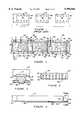
- FIG. 1is a schematic plan view of a plurality of prior art semiconductor dice
- FIG. 2is a schematic plan view, partially cut away, of a polymer lead frame constructed in accordance with the invention, and having the plurality of dice mounted thereon;
- FIG. 3is an enlarged schematic cross sectional view taken along section line 3--3 of FIG. 2 showing bonding of the dice to the lead frame;
- FIG. 4is an enlarged side elevational view of a die that has been singulated from the polymer lead frame with a segment of polymer film bonded thereto to form a polymer interconnect;
- FIG. 5is a side elevation view of the die taken along line 5--5 of FIG. 4 illustrating edge contacts on the polymer film;
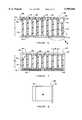
- FIG. 6is a front elevation view, partially cut away and cross sectioned, illustrating a semiconductor package constructed in accordance with the invention
- FIG. 7is a plan view, partially cut away and cross sectioned, of the package.
- FIG. 8is a side elevation view of the package
- FIG. 9is an enlarged schematic view of a portion of the package taken along section line 9--9 of FIG. 6 showing resilient contacts on a substrate of the package;
- FIG. 9Ais an enlarged schematic view equivalent to FIG. 9 of alternate embodiment resilient contacts
- FIG. 10is a schematic cross sectional view taken along section line 10--10 of FIG. 9;
- FIG. 11is a schematic cross sectional view of an alternate embodiment semiconductor die having the polymer film bonded thereto with a compressible member therebetween;
- FIG. 12is a schematic cross sectional view of an alternate embodiment semiconductor die having a polymer film bonded thereto with a cantilevered spring contact;
- FIG. 13is a schematic plan view of the polymer film of FIG. 12 shown separately and illustrating cut outs on the polymer film for forming the spring contacts;
- FIG. 14is a schematic perspective view of an alternate embodiment semiconductor die having edge contacts on a longitudinal edge in electrical engagement with mating electrodes on a substrate;
- FIG. 15is a schematic side elevation view of an alternate embodiment semiconductor die having interlevel conductors and mating contacts on a substrate.
- Each die 12is generally rectangular in shape and includes a face 10 having patterns of bond pads 14 thereon. Each die 12 also includes four sides (or edges) that are generally perpendicular to the face 10, and an opposing back side that is generally parallel to the face 10.
- the bond pads 14 on the face 10 of the die 12are in electrical communication with integrated circuits contained on the die 12.
- the bond pads 14comprise a thin film of aluminum embedded in a passivation layer 16 (FIG. 3).
- the die 12includes eight bond pads 14 arranged in two parallel, spaced rows along opposite sides of the die 12. However, in actual practice the die 12 will typically contain 20-50 or more bond pads 14. Also, rather than being formed along the sides of the die 12, the bond pads 14 can be formed along a center line of the die 12, or in other patterns as required.
- a lead frame 18 containing multiple polymer interconnects 20is provided. Each polymer interconnect 20 is configured to mount a single semiconductor die 12 thereto.
- the lead frame 18comprises a multi layered tape similar to conventional TAB tape (tape automated bonding tape) used for semiconductor packaging.
- Representative commercial productsinclude "ASMAT” manufactured by Nitto Denko, “GOLD DOT” manufactured by Packard Hughes, and "Z-LINK” manufactured by Sheldahl.
- the lead frame 18includes siderails 22, 24 having openings 26 that permit handling by automated machinery.
- the lead frame 18also includes connecting segments 28 between the polymer interconnects 20. Following attachment of the dice 12 to the lead frame 18, the connecting segments 28 will be severed, such as by cutting, to separate the individual interconnects 20 from the lead frame 18.
- Each polymer interconnect 20includes a length of polymer tape 30 having patterns of conductors 32 and microbumps 34 formed thereon.
- the polymer tape 30comprises an electrically insulating elastomeric film, such as polyimide, having a thickness of about 0.5 to 10 mils.
- the conductors 32can be formed on a first side of the polymer tape 30, and the microbumps 34 can be formed on an opposing second side of the polymer tape 30. Vias 36 through the polymer tape 30 electrically connect the microbumps 34 to the conductors 32.
- the microbumps 34are configured for bonding to the bond pads 14 on the dice 12. As such, a pattern of the microbumps 34 matches a pattern of the bond pads 14 on the dice 12. A representative diameter of the microbumps 34 can be from 5 mils to 50 mils.
- the microbumps 34can be formed of one or more layers of metal using a suitable deposition process such as electrodeposition. Suitable metals for the microbumps 34 include solder, Ni, Au Cu, and alloys of these metals. Alternately, the microbumps 34 can comprise a conductive polymer, such as an anisotropic or isotropic adhesive, deposited by stenciling or screen printing.
- the dice 12can be flip chip mounted to the polymer interconnects 20 by bonding the microbumps 34 to the bond pads 14 using a thermal process such as solder reflow, welding or brazing. Alternately for conductive adhesive microbumps 24, a curing process can be used to bond the microbumps 34 to the bond pads 14.
- each polymer interconnect 20will subsequently be folded along a fold line 40 so that the edge contacts 42 align with a side 44 (FIG. 5) of a die 12.
- a length "S1" of the segment between the fold line 40 and edge 38 of each polymer interconnect 20is approximately equal to a thickness "T" (FIG. 4) of the die 12.
- a length "S1" of the segment between the fold line 40 and edge 39 of each polymer interconnect 20is approximately equal to a length of the die 12.
- FIG. 4illustrates a die 12 that has been bonded to a polymer interconnect 20, and separated from the lead frame 18. Following the separation process, the polymer tape 30 has been folded along fold line 40. Preferably the fold line 40 aligns with an edge or corner of the die 12. Folding of the polymer tape 30 can be accomplished using a bending tool or fixture.
- an adhesive layer 46can be used to bond the folded portion of the polymer tape 30 to the side 44 of the die 12.
- One suitable adhesivecomprises a silicone elastomer such as "ZYMET" manufactured by Zymet, Inc., East Hanover, N.J.
- the edge contacts 42 on the polymer interconnect 20align with the side 44 of the die 12. This permits the die 12 to be “edge” mounted on the side 44 and electrically connected using the edge contacts 42.
- the package 48includes a housing 50 having a plurality of separate cavities 56 configured to contain a plurality of semiconductor dice 12.
- the package 48includes a substrate 52 attached to the housing 50 and configured to provide electrical connections to the dice 12.
- the package 48also includes a force applying mechanism 54 configured to bias the dice 12 against the substrate 52.
- the housing 50is a molded plastic structure that includes sidewalls 58, 60; end walls 62, 64; and partitions 66 which define the cavities 56.
- the housing 50can be formed separately, and then attached to the substrate 52, using an adhesive, such as silicone or an epoxy.
- the housing 50includes eight cavities 56 for retaining eight dice 12.
- Each cavity 56has a width "W1" that is slightly larger than the thickness "T" (FIG. 4) of a single die 12 and an attached polymer interconnect 20.
- a width "W2" of each cavity 56is slightly larger than the width "W1" (FIG. 1) of a single die 12.
- a depth “D” of each cavity 56is slightly less than a length "L” (FIG. 1) of a single die 12 and an attached polymer interconnect 20. The dice 12 can thus be slid into the cavities 56 and retained by the dimensions of the cavities 56.
- the substrate 52comprises a rigid, electrically insulating material, such as a glass filled resin (FR-4), or ceramic.
- the substrate 52can also comprise silicon having an insulating layer, such as SiO 2 , or polyimide formed thereon.
- a single housing 50is mounted to the substrate 52.
- the substrate 52can also be in the configuration of a circuit board, or multi chip module substrate having multiple housings 50 mounted thereon.
- the substrate 52includes an edge connector 68.
- the edge connector 68can be configured for removable electrical connection to a mating electrical receptacle (not shown) on a circuit board, control panel or other electronic assembly.
- the substrate 52can be provided with external contacts such as leads, pins or balls.
- the substrate 52includes resilient contacts 70 configured to electrically engage the edge contacts 42 on the polymer interconnects 20 attached to the dice 12.
- the resilient contacts 70comprise metal or conductive polymer microbumps, similar to the microbumps 34 (FIG. 3) previously described.
- the resilient contacts 70are adapted to form non-bonded rather than bonded connections with the edge contacts 42.
- resilient contacts 70Acan comprise planar pads and edge contacts 42A can comprise bumps or spheres of a conductive material.
- the resilient contacts 70are in electrical communication with patterns of conductors 74 mounted on a polymer tape 72.
- the resilient contacts 70, conductors 74 and polymer tape 72can comprise multi layered TAB tape as previously described.
- the polymer tape 72can include an integral ground plane for matching impedance and reducing cross talk between the conductors 74.
- the polymer tape 72can be adhesively bonded, or laminated, to the substrate 52.
- the polymer tape 72can be mounted to the substrate 52 with the conductors 74 thereon in electrical communication with the edge connector 68 (FIG. 7) on the substrate 52.
- the partitions 66 on the housing 50include openings 76 proximate to the substrate 52 to provide clearance for the polymer tape 72 and the conductors 74.
- a plurality of compressible members 78can be mounted between the substrate 52 and polymer tape 72 to provide additional resiliency or compliancy for the resilient contacts 70.
- the compressible members 78can comprise an elastomeric material, such as silicone, in a foam, gel or molded configuration. Alternately, the compressible members can comprise cured silicone strips or dots, or alternately deposited dots or strips, which are then cured. Silicone strips or dots are commercially available from Dow Chemical Co.
- the force applying mechanism 54includes a lid 80 which attaches to the housing 50.
- the force applying mechanismalso includes a compressible member 82 which bias the dice 12 against the substrate 52.
- the lid 80comprises a one piece molded plastic member.
- the lid 80can also be formed of metal or other rigid material.
- the lid 80includes latching portions 84 which engage mating indentations 86 formed in the end walls 62, 64 of the housing 50.
- the latching portions 84can be molded integrally with the lid 80, or formed as separate members attached to the lid 80.
- the compressible member 82can be attached to the lid 80 or can be a separate member placed within the housing 50 for contact by the lid 80.
- the compressible member 82is adapted to exert a force "F" (FIG. 9) on the dice 12. This biases the dice 12 against the substrate 52 and maintains electrical contact between the edge contacts 42 (FIG. 10) on the polymer interconnects 20, and the resilient contacts 70 (FIG. 10) on the polymer tape 72.
- the compressible member 82can comprise a compressible elastomeric material, such as silicone. Suitable elastomeric materials include “PORON” and “BISCO” available from a Dow Chemical subsidiary. Rather than being formed of elastomeric materials, the compressible member 82 can comprise a liquid or gas filled bladder. This type of bladder is available from Paratech of Frankfort, Ill. under the trademark "MAXI FORCE AIR BAG”.
- the lid 80 and compressible member 82can be detached from the housing 50 for removing the dice 12.
- the dice 12can then be replaced with other dice without requiring a bonded connection with the substrate 52.
- a bonding processsuch as solder reflow, soldering, brazing, or welding can be employed.
- a conductive polymer materialsuch as an isotropic or anisotropic adhesive, can also be employed to make bonded connections.
- the conductive polymer materialcan be applied to the edge contacts 42 (FIG. 10), or to the resilient contacts 70 (FIG.
- edge contacts 42 or the resilient contacts 70can comprise a conductive polymer material that is cured to form a permanent conductive bond.
- the polymer interconnect 20Bincludes a polymer tape 30B having conductors 32B and edge contacts 42B formed substantially as previously described for tape 30, conductors 32 and contacts 42.
- the polymer interconnect 20Balso includes a compressible member 88 mounted between the side 44 of the die 12 and the polymer tape 30B.
- the compressible member 88can be formed of a resilient polymeric material such as silicone or rubber.
- the polymer interconnect 20Cincludes a polymer tape 30C having conductors 32C and edge contacts 42C substantially as previously described.
- end portions 92 of the conductors 32Care cantilevered from the side 44 of the die 12 to form resilient spring contacts, similar in shape to "gull wing" contacts.
- the cantilevered end portions 92provide a spring force for biasing the edge contacts 42C against the resilient contacts 70 (FIG. 10).
- the end portions 92 cut outs 90can be formed in the polymer tape 30C.
- the conductors 32Ccan be formed of a naturally resilient material such as beryllium copper.
- the polymer interconnect 20Dis formed substantially as previously described but with edge contacts 42D formed on a side 94 of the die 12.
- the resilient contacts 70A on the substrate 52comprise parallel spaced conductive traces.
- the polymer interconnect 20Eis formed substantially as previously described but includes a polymer interconnect 20E having multi level conductors 32E, 32F formed on a polymer tape 30D.
- conductors 32Ecan be formed on a first side of the tape 30D
- conductors 32Fcan be formed on an opposing second side of the tape 30D.
- one level of conductorscan be a ground plane for matching the impedance of the conductors as previously described.
- one level of conductorscan function as a voltage plane.
- the multi level conductors 32E, 32Finclude edge contacts 42E and 42F respectively. The edge contacts 42E and 42F mate with resilient contacts 70E and 70F on the substrate 52.
- the inventionprovides an improved semiconductor package and method of fabrication.
- One advantage of the packageis assembly, disassembly and re-assembly are facilitated by non-bonded electrical connections.
- the edge mounting of the diceallow high device densities in a relatively compact package.
- an impedance of conductors on the polymer interconnects and on the substratecan be matched by providing an integral ground plane.
Landscapes
- Engineering & Computer Science (AREA)
- Power Engineering (AREA)
- Microelectronics & Electronic Packaging (AREA)
- Computer Hardware Design (AREA)
- Physics & Mathematics (AREA)
- Condensed Matter Physics & Semiconductors (AREA)
- General Physics & Mathematics (AREA)
- Wire Bonding (AREA)
Abstract
Description
Claims (22)
Priority Applications (2)
| Application Number | Priority Date | Filing Date | Title |
|---|---|---|---|
| US09/082,093US5990566A (en) | 1998-05-20 | 1998-05-20 | High density semiconductor package |
| US09/349,417US6210993B1 (en) | 1998-05-20 | 1999-07-06 | High density semiconductor package and method of fabrication |
Applications Claiming Priority (1)
| Application Number | Priority Date | Filing Date | Title |
|---|---|---|---|
| US09/082,093US5990566A (en) | 1998-05-20 | 1998-05-20 | High density semiconductor package |
Related Child Applications (1)
| Application Number | Title | Priority Date | Filing Date |
|---|---|---|---|
| US09/349,417DivisionUS6210993B1 (en) | 1998-05-20 | 1999-07-06 | High density semiconductor package and method of fabrication |
Publications (1)
| Publication Number | Publication Date |
|---|---|
| US5990566Atrue US5990566A (en) | 1999-11-23 |
Family
ID=22169029
Family Applications (2)
| Application Number | Title | Priority Date | Filing Date |
|---|---|---|---|
| US09/082,093Expired - LifetimeUS5990566A (en) | 1998-05-20 | 1998-05-20 | High density semiconductor package |
| US09/349,417Expired - LifetimeUS6210993B1 (en) | 1998-05-20 | 1999-07-06 | High density semiconductor package and method of fabrication |
Family Applications After (1)
| Application Number | Title | Priority Date | Filing Date |
|---|---|---|---|
| US09/349,417Expired - LifetimeUS6210993B1 (en) | 1998-05-20 | 1999-07-06 | High density semiconductor package and method of fabrication |
Country Status (1)
| Country | Link |
|---|---|
| US (2) | US5990566A (en) |
Cited By (96)
| Publication number | Priority date | Publication date | Assignee | Title |
|---|---|---|---|---|
| US6210993B1 (en) | 1998-05-20 | 2001-04-03 | Micron Technology, Inc. | High density semiconductor package and method of fabrication |
| US6232666B1 (en) | 1998-12-04 | 2001-05-15 | Mciron Technology, Inc. | Interconnect for packaging semiconductor dice and fabricating BGA packages |
| US6259036B1 (en) | 1998-04-13 | 2001-07-10 | Micron Technology, Inc. | Method for fabricating electronic assemblies using semi-cured conductive elastomeric bumps |
| US6281044B1 (en) | 1995-07-31 | 2001-08-28 | Micron Technology, Inc. | Method and system for fabricating semiconductor components |
| US6300687B1 (en)* | 1998-06-26 | 2001-10-09 | International Business Machines Corporation | Micro-flex technology in semiconductor packages |
| US6320253B1 (en)* | 1998-09-01 | 2001-11-20 | Micron Technology, Inc. | Semiconductor device comprising a socket and method for forming same |
| US20020017709A1 (en)* | 2000-06-07 | 2002-02-14 | Yoshiyuki Yanagisawa | Assembly jig and manufacturing method of multilayer semiconductor device |
| US6383839B2 (en) | 1998-01-27 | 2002-05-07 | Micron Technology, Inc. | Vertically mountable semiconductor device and methods |
| US20020140077A1 (en)* | 1998-02-27 | 2002-10-03 | Micron Technology, Inc. | Multichip semiconductor package |
| US6462271B2 (en) | 2000-12-27 | 2002-10-08 | International Business Machines Corporation | Capping structure for electronics package undergoing compressive socket actuation |
| US6466046B1 (en)* | 1998-12-18 | 2002-10-15 | Fujitsu Limited | Contactor for semiconductor devices, a testing apparatus using such contactor, a testing method using such contactor, and a method of cleaning such contactor |
| US6472239B2 (en) | 2001-04-02 | 2002-10-29 | Micron Technology, Inc. | Method for fabricating semiconductor components |
| US6548376B2 (en) | 2001-08-30 | 2003-04-15 | Micron Technology, Inc. | Methods of thinning microelectronic workpieces |
| US20030071341A1 (en)* | 2001-10-16 | 2003-04-17 | Jeung Boon Suan | Apparatus and method for leadless packaging of semiconductor devices |
| US6552910B1 (en) | 2000-06-28 | 2003-04-22 | Micron Technology, Inc. | Stacked-die assemblies with a plurality of microelectronic devices and methods of manufacture |
| US6558600B1 (en) | 2000-05-04 | 2003-05-06 | Micron Technology, Inc. | Method for packaging microelectronic substrates |
| US6560117B2 (en) | 2000-06-28 | 2003-05-06 | Micron Technology, Inc. | Packaged microelectronic die assemblies and methods of manufacture |
| US6564979B2 (en) | 2001-07-18 | 2003-05-20 | Micron Technology, Inc. | Method and apparatus for dispensing adhesive on microelectronic substrate supports |
| US6576494B1 (en) | 2000-06-28 | 2003-06-10 | Micron Technology, Inc. | Recessed encapsulated microelectronic devices and methods for formation |
| US6582990B2 (en) | 2001-08-24 | 2003-06-24 | International Rectifier Corporation | Wafer level underfill and interconnect process |
| US6600171B1 (en) | 2001-04-02 | 2003-07-29 | Micron Technology, Inc. | Semiconductor component and system for fabricating contacts on semiconductor components |
| US6607937B1 (en) | 2000-08-23 | 2003-08-19 | Micron Technology, Inc. | Stacked microelectronic dies and methods for stacking microelectronic dies |
| US6622380B1 (en) | 2002-02-12 | 2003-09-23 | Micron Technology, Inc. | Methods for manufacturing microelectronic devices and methods for mounting microelectronic packages to circuit boards |
| US20030197281A1 (en)* | 2002-04-19 | 2003-10-23 | Farnworth Warren M. | Integrated circuit package having reduced interconnects |
| US6638595B2 (en) | 2000-06-28 | 2003-10-28 | Micron Technology, Inc. | Method and apparatus for reduced flash encapsulation of microelectronic devices |
| US6653173B2 (en) | 2000-06-16 | 2003-11-25 | Micron Technology, Inc. | Method and apparatus for packaging a microelectronic die |
| US6656769B2 (en) | 2000-05-08 | 2003-12-02 | Micron Technology, Inc. | Method and apparatus for distributing mold material in a mold for packaging microelectronic devices |
| US20030232488A1 (en)* | 2002-06-14 | 2003-12-18 | Chua Swee Kwang | Wafer level packaging |
| US20040026773A1 (en)* | 2002-08-08 | 2004-02-12 | Koon Eng Meow | Packaged microelectronic components |
| US20040026776A1 (en)* | 2002-08-08 | 2004-02-12 | Brand Joseph M. | Microelectronic devices and methods for manufacturing and operating packaged microelectronic device assemblies |
| US20040031621A1 (en)* | 2002-08-19 | 2004-02-19 | Heng Puah Kia | Packaged microelectronic component assemblies |
| US6696754B2 (en)* | 1997-05-27 | 2004-02-24 | Fujitsu Limited | Semiconductor module including a plurality of semiconductor devices detachably |
| US20040038447A1 (en)* | 2002-08-21 | 2004-02-26 | Corisis David J | Packaged microelectronic devices and methods for assembling microelectronic devices |
| US20040035917A1 (en)* | 2002-08-22 | 2004-02-26 | Michel Koopmans | Apparatus and method for depositing and reflowing solder paste on a microelectronic workpiece |
| US20040070087A1 (en)* | 2002-10-11 | 2004-04-15 | Siliconware Precision Industries Co., Ltd. | Semiconductor package with enhanced chip groundability and method of fabricating the same |
| US6750547B2 (en) | 2001-12-26 | 2004-06-15 | Micron Technology, Inc. | Multi-substrate microelectronic packages and methods for manufacture |
| US20040159946A1 (en)* | 2001-12-26 | 2004-08-19 | Stephen Moxham | Microelectronic assemblies, electronic devices, and apparatuses for supporting microelectronic substrates |
| US20040173899A1 (en)* | 2003-03-04 | 2004-09-09 | Peng Neo Chee | Microelectronic component assemblies employing lead frames having reduced-thickness inner lengths |
| US20040178495A1 (en)* | 2003-03-14 | 2004-09-16 | Yean Tay Wuu | Microelectronic devices and methods for packaging microelectronic devices |
| US6796028B2 (en) | 2000-08-23 | 2004-09-28 | Micron Technology, Inc. | Method of Interconnecting substrates for electrical coupling of microelectronic components |
| US20040188400A1 (en)* | 2001-09-10 | 2004-09-30 | Micron Technology, Inc. | Wafer dicing device and method |
| US6838760B1 (en) | 2000-08-28 | 2005-01-04 | Micron Technology, Inc. | Packaged microelectronic devices with interconnecting units |
| US20050019984A1 (en)* | 2000-08-09 | 2005-01-27 | Tongbi Jiang | Multiple substrate microelectronic devices and methods of manufacture |
| US20050019988A1 (en)* | 2002-04-04 | 2005-01-27 | Tongbi Jiang | Method and apparatus for attaching microelectronic substrates and support members |
| US20050026395A1 (en)* | 2002-01-16 | 2005-02-03 | Micron Technology, Inc. | Fabrication of stacked microelectronic devices |
| US20050029668A1 (en)* | 2001-10-08 | 2005-02-10 | Micron Technology, Inc. | Apparatus and method for packaging circuits |
| US20050046431A1 (en)* | 2003-09-03 | 2005-03-03 | Kirby Kyle K. | Probe card for use with microelectronic components,and methods for making same |
| US20050045378A1 (en)* | 2003-08-29 | 2005-03-03 | Heng Mung Suan | Stacked microfeature devices and associated methods |
| US6876066B2 (en) | 2001-08-29 | 2005-04-05 | Micron Technology, Inc. | Packaged microelectronic devices and methods of forming same |
| US6879050B2 (en) | 2003-02-11 | 2005-04-12 | Micron Technology, Inc. | Packaged microelectronic devices and methods for packaging microelectronic devices |
| US20050093174A1 (en)* | 2003-10-31 | 2005-05-05 | Seng Eric T.S. | Reduced footprint packaged microelectronic components and methods for manufacturing such microelectronic components |
| US20050104171A1 (en)* | 2003-11-13 | 2005-05-19 | Benson Peter A. | Microelectronic devices having conductive complementary structures and methods of manufacturing microelectronic devices having conductive complementary structures |
| US20050104228A1 (en)* | 2003-11-13 | 2005-05-19 | Rigg Sidney B. | Microelectronic devices, methods for forming vias in microelectronic devices, and methods for packaging microelectronic devices |
| US6921860B2 (en) | 2003-03-18 | 2005-07-26 | Micron Technology, Inc. | Microelectronic component assemblies having exposed contacts |
| US6951982B2 (en) | 2002-11-22 | 2005-10-04 | Micron Technology, Inc. | Packaged microelectronic component assemblies |
| US6979595B1 (en) | 2000-08-24 | 2005-12-27 | Micron Technology, Inc. | Packaged microelectronic devices with pressure release elements and methods for manufacturing and using such packaged microelectronic devices |
| US20060017177A1 (en)* | 2004-07-23 | 2006-01-26 | Seng Eric T S | Microelectronic component assemblies with recessed wire bonds and methods of making same |
| US20060040428A1 (en)* | 2004-08-19 | 2006-02-23 | Johnson Mark S | Conductive structures for microfeature devices and methods for fabricating microfeature devices |
| US20060046346A1 (en)* | 2004-09-01 | 2006-03-02 | Benson Peter A | Methods for packaging microfeature devices and microfeature devices formed by such methods |
| US20060044773A1 (en)* | 2004-08-25 | 2006-03-02 | Micron Technology, Inc. | Methods and apparatuses for transferring heat from stacked microfeature devices |
| US20060043611A1 (en)* | 2004-09-01 | 2006-03-02 | Kinsman Larry D | Reduced-dimension microelectronic component assemblies with wire bonds and methods of making same |
| US7037756B1 (en) | 2001-08-30 | 2006-05-02 | Micron Technology, Inc. | Stacked microelectronic devices and methods of fabricating same |
| US20060292858A1 (en)* | 2002-07-18 | 2006-12-28 | Micron Technology, Inc. | Techniques to create low K ILD for beol |
| US20070045872A1 (en)* | 2005-08-31 | 2007-03-01 | Fee Setho S | Microelectronic devices having intermediate contacts for connection to interposer substrates, and associated methods of packaging microelectronic devices with intermediate contacts |
| US20070045862A1 (en)* | 2005-09-01 | 2007-03-01 | Micron Technology, Inc. | Stacked microelectronic devices and methods for manufacturing microelectronic devices |
| US20070045803A1 (en)* | 2005-08-26 | 2007-03-01 | Micron Technology, Inc. | Microelectronic device packages, stacked microelectronic device packages, and methods for manufacturing microelectronic devices |
| US20070045796A1 (en)* | 2005-08-19 | 2007-03-01 | Micron Technology, Inc. | Microelectronic devices, stacked microelectronic devices, and methods for manufacturing microelectronic devices |
| US20070045797A1 (en)* | 2005-08-24 | 2007-03-01 | Micron Technology, Inc. | Microelectronic devices and microelectronic support devices, and associated assemblies and methods |
| US20070045807A1 (en)* | 2005-09-01 | 2007-03-01 | Micron Technology, Inc. | Microelectronic devices and methods for manufacturing microelectronic devices |
| US7198693B1 (en) | 2002-02-20 | 2007-04-03 | Micron Technology, Inc. | Microelectronic device having a plurality of stacked dies and methods for manufacturing such microelectronic assemblies |
| US20070166883A1 (en)* | 2006-01-18 | 2007-07-19 | Shun-Ta Wang | Method of wafer level packaging and cutting |
| US7259451B2 (en) | 2003-08-29 | 2007-08-21 | Micron Technology, Inc. | Invertible microfeature device packages |
| US20070210441A1 (en)* | 2006-03-08 | 2007-09-13 | Micron Technology, Inc. | Microelectronic device assemblies including assemblies with recurved leadframes, and associated methods |
| US7273769B1 (en) | 2000-08-16 | 2007-09-25 | Micron Technology, Inc. | Method and apparatus for removing encapsulating material from a packaged microelectronic device |
| US20070228577A1 (en)* | 2006-03-29 | 2007-10-04 | Micron Technology, Inc. | Packaged microelectronic devices recessed in support member cavities, and associated methods |
| US20080012110A1 (en)* | 2006-07-17 | 2008-01-17 | Micron Technology, Inc. | Microelectronic packages with leadframes, including leadframes configured for stacked die packages, and associated systems and methods |
| US20080048316A1 (en)* | 2006-08-25 | 2008-02-28 | Micron Technology, Inc. | Packaged microdevices and methods for manufacturing packaged microdevices |
| US20080128900A1 (en)* | 2006-12-04 | 2008-06-05 | Micron Technology, Inc. | Packaged microelectronic devices and methods for manufacturing packaged microelectronic devices |
| US20080224291A1 (en)* | 2007-03-13 | 2008-09-18 | Micron Technology, Inc. | Packaged semiconductor components having substantially rigid support members and methods of packaging semiconductor components |
| US20080224329A1 (en)* | 2007-03-13 | 2008-09-18 | Micron Technology, Inc. | Packaged microelectronic devices and methods for manufacturing packaged microelectronic devices |
| US7518237B2 (en) | 2005-02-08 | 2009-04-14 | Micron Technology, Inc. | Microfeature systems including adhered microfeature workpieces and support members |
| US7622377B2 (en) | 2005-09-01 | 2009-11-24 | Micron Technology, Inc. | Microfeature workpiece substrates having through-substrate vias, and associated methods of formation |
| US7671459B2 (en) | 2006-02-08 | 2010-03-02 | Micron Technologies, Inc. | Microelectronic devices, stacked microelectronic devices, and methods for manufacturing such devices |
| US7712211B2 (en) | 2003-05-06 | 2010-05-11 | Micron Technology, Inc. | Method for packaging circuits and packaged circuits |
| US7759221B2 (en) | 2005-12-29 | 2010-07-20 | Micron Technology, Inc. | Methods for packaging microelectronic devices and microelectronic devices formed using such methods |
| US20100181679A1 (en)* | 2007-06-07 | 2010-07-22 | Commissariat A L'energie Atomique | 3d integration of vertical components in reconstituted substrates |
| US7807505B2 (en) | 2005-08-30 | 2010-10-05 | Micron Technology, Inc. | Methods for wafer-level packaging of microfeature devices and microfeature devices formed using such methods |
| US7833456B2 (en) | 2007-02-23 | 2010-11-16 | Micron Technology, Inc. | Systems and methods for compressing an encapsulant adjacent a semiconductor workpiece |
| US7843050B2 (en) | 2007-07-24 | 2010-11-30 | Micron Technology, Inc. | Microelectronic die packages with metal leads, including metal leads for stacked die packages, and associated systems and methods |
| US7910385B2 (en) | 2006-05-12 | 2011-03-22 | Micron Technology, Inc. | Method of fabricating microelectronic devices |
| US7947529B2 (en) | 2007-08-16 | 2011-05-24 | Micron Technology, Inc. | Microelectronic die packages with leadframes, including leadframe-based interposer for stacked die packages, and associated systems and methods |
| US8084866B2 (en) | 2003-12-10 | 2011-12-27 | Micron Technology, Inc. | Microelectronic devices and methods for filling vias in microelectronic devices |
| US20120119345A1 (en)* | 2010-11-15 | 2012-05-17 | Cho Sungwon | Integrated circuit packaging system with device mount and method of manufacture thereof |
| US8541262B2 (en) | 2010-09-02 | 2013-09-24 | Taiwan Semiconductor Manufacturing Company, Ltd. | Die edge contacts for semiconductor devices |
| US9165888B2 (en) | 2008-09-11 | 2015-10-20 | Micron Technology, Inc. | Interconnect structures for stacked dies, including penetrating structures for through-silicon vias, and associated systems and methods |
| US20180047706A1 (en)* | 2016-08-09 | 2018-02-15 | Sandisk Information Technology (Shanghai) Co., Ltd. | Vertical semiconductor device |
Families Citing this family (6)
| Publication number | Priority date | Publication date | Assignee | Title |
|---|---|---|---|---|
| US6153929A (en)* | 1998-08-21 | 2000-11-28 | Micron Technology, Inc. | Low profile multi-IC package connector |
| US20020117753A1 (en)* | 2001-02-23 | 2002-08-29 | Lee Michael G. | Three dimensional packaging |
| US7064010B2 (en)* | 2003-10-20 | 2006-06-20 | Micron Technology, Inc. | Methods of coating and singulating wafers |
| KR100609011B1 (en)* | 2003-12-05 | 2006-08-03 | 삼성전자주식회사 | Wafer level module and manufacturing method thereof |
| CN1624919A (en)* | 2003-12-05 | 2005-06-08 | 三星电子株式会社 | Wafer level electronic module with integral connector contacts and method of manufacturing the same |
| JP5742242B2 (en)* | 2011-01-21 | 2015-07-01 | セイコーエプソン株式会社 | Substrate connection method and semiconductor device manufacturing method |
Citations (10)
| Publication number | Priority date | Publication date | Assignee | Title |
|---|---|---|---|---|
| US5104324A (en)* | 1991-06-26 | 1992-04-14 | Amp Incorporated | Multichip module connector |
| US5107328A (en)* | 1991-02-13 | 1992-04-21 | Micron Technology, Inc. | Packaging means for a semiconductor die having particular shelf structure |
| US5138434A (en)* | 1991-01-22 | 1992-08-11 | Micron Technology, Inc. | Packaging for semiconductor logic devices |
| US5281852A (en)* | 1991-12-10 | 1994-01-25 | Normington Peter J C | Semiconductor device including stacked die |
| US5347159A (en)* | 1990-09-24 | 1994-09-13 | Tessera, Inc. | Semiconductor chip assemblies with face-up mounting and rear-surface connection to substrate |
| US5593927A (en)* | 1993-10-14 | 1997-01-14 | Micron Technology, Inc. | Method for packaging semiconductor dice |
| US5674785A (en)* | 1995-11-27 | 1997-10-07 | Micron Technology, Inc. | Method of producing a single piece package for semiconductor die |
| US5678301A (en)* | 1991-06-04 | 1997-10-21 | Micron Technology, Inc. | Method for forming an interconnect for testing unpackaged semiconductor dice |
| US5696033A (en)* | 1995-08-16 | 1997-12-09 | Micron Technology, Inc. | Method for packaging a semiconductor die |
| US5832601A (en)* | 1993-11-16 | 1998-11-10 | Form Factor, Inc. | Method of making temporary connections between electronic components |
Family Cites Families (8)
| Publication number | Priority date | Publication date | Assignee | Title |
|---|---|---|---|---|
| US5067233A (en)* | 1989-07-24 | 1991-11-26 | Grumman Aerospace Corporation | Method of forming an integrated circuit module |
| CA2118994A1 (en)* | 1993-06-21 | 1994-12-22 | Claude L. Bertin | Polyimide-insulated cube package of stacked semiconductor device chips |
| US5767443A (en)* | 1993-07-10 | 1998-06-16 | Micron Technology, Inc. | Multi-die encapsulation device |
| SE516207C2 (en)* | 1996-11-26 | 2001-12-03 | Ericsson Telefon Ab L M | Method and apparatus for surface mounting a component standing on a carrier |
| US5933712A (en)* | 1997-03-19 | 1999-08-03 | The Regents Of The University Of California | Attachment method for stacked integrated circuit (IC) chips |
| US5892287A (en)* | 1997-08-18 | 1999-04-06 | Texas Instruments | Semiconductor device including stacked chips having metal patterned on circuit surface and on edge side of chip |
| US5995378A (en)* | 1997-12-31 | 1999-11-30 | Micron Technology, Inc. | Semiconductor device socket, assembly and methods |
| US5990566A (en) | 1998-05-20 | 1999-11-23 | Micron Technology, Inc. | High density semiconductor package |
- 1998
- 1998-05-20USUS09/082,093patent/US5990566A/ennot_activeExpired - Lifetime
- 1999
- 1999-07-06USUS09/349,417patent/US6210993B1/ennot_activeExpired - Lifetime
Patent Citations (10)
| Publication number | Priority date | Publication date | Assignee | Title |
|---|---|---|---|---|
| US5347159A (en)* | 1990-09-24 | 1994-09-13 | Tessera, Inc. | Semiconductor chip assemblies with face-up mounting and rear-surface connection to substrate |
| US5138434A (en)* | 1991-01-22 | 1992-08-11 | Micron Technology, Inc. | Packaging for semiconductor logic devices |
| US5107328A (en)* | 1991-02-13 | 1992-04-21 | Micron Technology, Inc. | Packaging means for a semiconductor die having particular shelf structure |
| US5678301A (en)* | 1991-06-04 | 1997-10-21 | Micron Technology, Inc. | Method for forming an interconnect for testing unpackaged semiconductor dice |
| US5104324A (en)* | 1991-06-26 | 1992-04-14 | Amp Incorporated | Multichip module connector |
| US5281852A (en)* | 1991-12-10 | 1994-01-25 | Normington Peter J C | Semiconductor device including stacked die |
| US5593927A (en)* | 1993-10-14 | 1997-01-14 | Micron Technology, Inc. | Method for packaging semiconductor dice |
| US5832601A (en)* | 1993-11-16 | 1998-11-10 | Form Factor, Inc. | Method of making temporary connections between electronic components |
| US5696033A (en)* | 1995-08-16 | 1997-12-09 | Micron Technology, Inc. | Method for packaging a semiconductor die |
| US5674785A (en)* | 1995-11-27 | 1997-10-07 | Micron Technology, Inc. | Method of producing a single piece package for semiconductor die |
Cited By (317)
| Publication number | Priority date | Publication date | Assignee | Title |
|---|---|---|---|---|
| US6626222B1 (en) | 1995-07-31 | 2003-09-30 | Micron Technology, Inc. | System for fabricating semiconductor components |
| US6281044B1 (en) | 1995-07-31 | 2001-08-28 | Micron Technology, Inc. | Method and system for fabricating semiconductor components |
| US6696754B2 (en)* | 1997-05-27 | 2004-02-24 | Fujitsu Limited | Semiconductor module including a plurality of semiconductor devices detachably |
| US6383839B2 (en) | 1998-01-27 | 2002-05-07 | Micron Technology, Inc. | Vertically mountable semiconductor device and methods |
| US6800942B1 (en)* | 1998-01-27 | 2004-10-05 | Micron Technology, Inc. | Vertically mountable semiconductor device and methods |
| US6906409B2 (en) | 1998-02-27 | 2005-06-14 | Micron Technology, Inc. | Multichip semiconductor package |
| US20050212143A1 (en)* | 1998-02-27 | 2005-09-29 | Micron Technology, Inc. | Multichip semiconductor package |
| US20020140077A1 (en)* | 1998-02-27 | 2002-10-03 | Micron Technology, Inc. | Multichip semiconductor package |
| US6259036B1 (en) | 1998-04-13 | 2001-07-10 | Micron Technology, Inc. | Method for fabricating electronic assemblies using semi-cured conductive elastomeric bumps |
| US6210993B1 (en) | 1998-05-20 | 2001-04-03 | Micron Technology, Inc. | High density semiconductor package and method of fabrication |
| US6300687B1 (en)* | 1998-06-26 | 2001-10-09 | International Business Machines Corporation | Micro-flex technology in semiconductor packages |
| US6534339B2 (en) | 1998-09-01 | 2003-03-18 | Larry Kinsman | Semiconductor device comprising a socket and method for forming same |
| US6320253B1 (en)* | 1998-09-01 | 2001-11-20 | Micron Technology, Inc. | Semiconductor device comprising a socket and method for forming same |
| US6232666B1 (en) | 1998-12-04 | 2001-05-15 | Mciron Technology, Inc. | Interconnect for packaging semiconductor dice and fabricating BGA packages |
| US6603325B2 (en) | 1998-12-18 | 2003-08-05 | Fujitsu Limited | Contactor for semiconductor devices, a testing apparatus using such contactor, a testing method using such contactor, and a method of cleaning such contactor |
| US6781395B2 (en) | 1998-12-18 | 2004-08-24 | Fujitsu Limited | Contactor for semiconductor devices, a testing apparatus using such contactor, a testing method using such contactor, and a method of cleaning such contactor |
| US6466046B1 (en)* | 1998-12-18 | 2002-10-15 | Fujitsu Limited | Contactor for semiconductor devices, a testing apparatus using such contactor, a testing method using such contactor, and a method of cleaning such contactor |
| US20030197501A1 (en)* | 1998-12-18 | 2003-10-23 | Fujitsu Limited | Contactor for semiconductor devices, a testing apparatus using such contactor, a testing method using such contactor, and a method of cleaning such contactor |
| US6558600B1 (en) | 2000-05-04 | 2003-05-06 | Micron Technology, Inc. | Method for packaging microelectronic substrates |
| US20030209831A1 (en)* | 2000-05-04 | 2003-11-13 | Williams Vernon M. | Method and apparatus for packaging microelectronic substrates |
| US6656769B2 (en) | 2000-05-08 | 2003-12-02 | Micron Technology, Inc. | Method and apparatus for distributing mold material in a mold for packaging microelectronic devices |
| US20020017709A1 (en)* | 2000-06-07 | 2002-02-14 | Yoshiyuki Yanagisawa | Assembly jig and manufacturing method of multilayer semiconductor device |
| US6664139B2 (en) | 2000-06-16 | 2003-12-16 | Micron Technology, Inc. | Method and apparatus for packaging a microelectronic die |
| US6653173B2 (en) | 2000-06-16 | 2003-11-25 | Micron Technology, Inc. | Method and apparatus for packaging a microelectronic die |
| US6683388B2 (en) | 2000-06-16 | 2004-01-27 | Micron Technology, Inc. | Method and apparatus for packaging a microelectronic die |
| US6677675B2 (en) | 2000-06-16 | 2004-01-13 | Micron Technology, Inc. | Microelectronic devices and microelectronic die packages |
| US6560117B2 (en) | 2000-06-28 | 2003-05-06 | Micron Technology, Inc. | Packaged microelectronic die assemblies and methods of manufacture |
| US6819003B2 (en) | 2000-06-28 | 2004-11-16 | Micron Technology Inc. | Recessed encapsulated microelectronic devices and methods for formation |
| US6841423B2 (en) | 2000-06-28 | 2005-01-11 | Micron Technology, Inc. | Methods for formation of recessed encapsulated microelectronic devices |
| US6576494B1 (en) | 2000-06-28 | 2003-06-10 | Micron Technology, Inc. | Recessed encapsulated microelectronic devices and methods for formation |
| US6638595B2 (en) | 2000-06-28 | 2003-10-28 | Micron Technology, Inc. | Method and apparatus for reduced flash encapsulation of microelectronic devices |
| US6552910B1 (en) | 2000-06-28 | 2003-04-22 | Micron Technology, Inc. | Stacked-die assemblies with a plurality of microelectronic devices and methods of manufacture |
| US6644949B2 (en) | 2000-06-28 | 2003-11-11 | Micron Technology, Inc. | Apparatus for reduced flash encapsulation of microelectronic devices |
| US7253025B2 (en) | 2000-08-09 | 2007-08-07 | Micron Technology, Inc. | Multiple substrate microelectronic devices and methods of manufacture |
| US7298031B1 (en) | 2000-08-09 | 2007-11-20 | Micron Technology, Inc. | Multiple substrate microelectronic devices and methods of manufacture |
| US20050019984A1 (en)* | 2000-08-09 | 2005-01-27 | Tongbi Jiang | Multiple substrate microelectronic devices and methods of manufacture |
| US7273769B1 (en) | 2000-08-16 | 2007-09-25 | Micron Technology, Inc. | Method and apparatus for removing encapsulating material from a packaged microelectronic device |
| US7405487B2 (en) | 2000-08-16 | 2008-07-29 | Micron Technology, Inc. | Method and apparatus for removing encapsulating material from a packaged microelectronic device |
| US6607937B1 (en) | 2000-08-23 | 2003-08-19 | Micron Technology, Inc. | Stacked microelectronic dies and methods for stacking microelectronic dies |
| US20040038449A1 (en)* | 2000-08-23 | 2004-02-26 | Corisis David J. | Stacked microelectronic dies and methods for stacking microelectronic dies |
| US20070210435A1 (en)* | 2000-08-23 | 2007-09-13 | Micron Technology, Inc. | Stacked microelectronic dies and methods for stacking microelectronic dies |
| US8587109B2 (en) | 2000-08-23 | 2013-11-19 | Micron Technology, Inc. | Stacked microelectronic dies and methods for stacking microelectronic dies |
| US6983551B2 (en) | 2000-08-23 | 2006-01-10 | Micron Technology, Inc. | Interconnecting substrates for electrical coupling of microelectronic components |
| US6982386B2 (en) | 2000-08-23 | 2006-01-03 | Micron Technology, Inc. | Interconnecting substrates for electrical coupling of microelectronic components |
| US6796028B2 (en) | 2000-08-23 | 2004-09-28 | Micron Technology, Inc. | Method of Interconnecting substrates for electrical coupling of microelectronic components |
| US8067827B2 (en) | 2000-08-23 | 2011-11-29 | Micron Technology, Inc. | Stacked microelectronic device assemblies |
| US7235871B2 (en) | 2000-08-23 | 2007-06-26 | Micron Technology, Inc. | Stacked microelectronic dies |
| US7049685B2 (en) | 2000-08-24 | 2006-05-23 | Micron Technology, Inc. | Packaged microelectronic devices with pressure release elements and methods for manufacturing and using such packaged microelectronic devices |
| US6979595B1 (en) | 2000-08-24 | 2005-12-27 | Micron Technology, Inc. | Packaged microelectronic devices with pressure release elements and methods for manufacturing and using such packaged microelectronic devices |
| US6838760B1 (en) | 2000-08-28 | 2005-01-04 | Micron Technology, Inc. | Packaged microelectronic devices with interconnecting units |
| US7332376B2 (en) | 2000-08-28 | 2008-02-19 | Micron Technology, Inc. | Method of encapsulating packaged microelectronic devices with a barrier |
| US7101737B2 (en) | 2000-08-28 | 2006-09-05 | Micron Technology, Inc. | Method of encapsulating interconnecting units in packaged microelectronic devices |
| US6462271B2 (en) | 2000-12-27 | 2002-10-08 | International Business Machines Corporation | Capping structure for electronics package undergoing compressive socket actuation |
| US6680213B2 (en) | 2001-04-02 | 2004-01-20 | Micron Technology, Inc. | Method and system for fabricating contacts on semiconductor components |
| US6600171B1 (en) | 2001-04-02 | 2003-07-29 | Micron Technology, Inc. | Semiconductor component and system for fabricating contacts on semiconductor components |
| US20050084986A1 (en)* | 2001-04-02 | 2005-04-21 | Hembree David R. | Semiconductor test board having laser patterned conductors |
| US6472239B2 (en) | 2001-04-02 | 2002-10-29 | Micron Technology, Inc. | Method for fabricating semiconductor components |
| US7049700B2 (en) | 2001-04-02 | 2006-05-23 | Micron Technology, Inc. | Semiconductor test board having laser patterned conductors |
| US6564979B2 (en) | 2001-07-18 | 2003-05-20 | Micron Technology, Inc. | Method and apparatus for dispensing adhesive on microelectronic substrate supports |
| US6967412B2 (en) | 2001-08-24 | 2005-11-22 | International Rectifier Corporation | Wafer level underfill and interconnect process |
| US6582990B2 (en) | 2001-08-24 | 2003-06-24 | International Rectifier Corporation | Wafer level underfill and interconnect process |
| US20030207490A1 (en)* | 2001-08-24 | 2003-11-06 | International Rectifier Corporation | Wafer level underfill and interconnect process |
| US6876066B2 (en) | 2001-08-29 | 2005-04-05 | Micron Technology, Inc. | Packaged microelectronic devices and methods of forming same |
| US6943450B2 (en) | 2001-08-29 | 2005-09-13 | Micron Technology, Inc. | Packaged microelectronic devices and methods of forming same |
| US7037756B1 (en) | 2001-08-30 | 2006-05-02 | Micron Technology, Inc. | Stacked microelectronic devices and methods of fabricating same |
| US6548376B2 (en) | 2001-08-30 | 2003-04-15 | Micron Technology, Inc. | Methods of thinning microelectronic workpieces |
| US20040188400A1 (en)* | 2001-09-10 | 2004-09-30 | Micron Technology, Inc. | Wafer dicing device and method |
| US7358154B2 (en) | 2001-10-08 | 2008-04-15 | Micron Technology, Inc. | Method for fabricating packaged die |
| US6894386B2 (en) | 2001-10-08 | 2005-05-17 | Micron Technology, Inc. | Apparatus and method for packaging circuits |
| US8115306B2 (en) | 2001-10-08 | 2012-02-14 | Round Rock Research, Llc | Apparatus and method for packaging circuits |
| US7675169B2 (en) | 2001-10-08 | 2010-03-09 | Micron Technology, Inc. | Apparatus and method for packaging circuits |
| US8138617B2 (en)* | 2001-10-08 | 2012-03-20 | Round Rock Research, Llc | Apparatus and method for packaging circuits |
| US20060084240A1 (en)* | 2001-10-08 | 2006-04-20 | Micron Technology, Inc. | Apparatus and method for packaging circuits |
| US20050029668A1 (en)* | 2001-10-08 | 2005-02-10 | Micron Technology, Inc. | Apparatus and method for packaging circuits |
| US6743696B2 (en) | 2001-10-16 | 2004-06-01 | Micron Technology, Inc. | Apparatus and method for leadless packaging of semiconductor devices |
| US20030071341A1 (en)* | 2001-10-16 | 2003-04-17 | Jeung Boon Suan | Apparatus and method for leadless packaging of semiconductor devices |
| US20030071338A1 (en)* | 2001-10-16 | 2003-04-17 | Jeung Boon Suan | Apparatus and method for leadless packaging of semiconductor devices |
| US20030080403A1 (en)* | 2001-10-16 | 2003-05-01 | Jeung Boon Suan | Apparatus and method for leadless packaging of semiconductor devices |
| US6747348B2 (en) | 2001-10-16 | 2004-06-08 | Micron Technology, Inc. | Apparatus and method for leadless packaging of semiconductor devices |
| US6787894B2 (en) | 2001-10-16 | 2004-09-07 | Micron Technology, Inc. | Apparatus and method for leadless packaging of semiconductor devices |
| US6790706B2 (en) | 2001-10-16 | 2004-09-14 | Micron Technology, Inc. | Apparatus and method for leadless packaging of semiconductor devices |
| US6870276B1 (en) | 2001-12-26 | 2005-03-22 | Micron Technology, Inc. | Apparatus for supporting microelectronic substrates |
| US6750547B2 (en) | 2001-12-26 | 2004-06-15 | Micron Technology, Inc. | Multi-substrate microelectronic packages and methods for manufacture |
| US6995026B2 (en) | 2001-12-26 | 2006-02-07 | Micron Technology, Inc. | Methods for coupling a flowable conductive material to microelectronic substrates |
| US20050242437A1 (en)* | 2001-12-26 | 2005-11-03 | Micron Technology, Inc. | Method and apparatus for supporting microelectronic substrates |
| US20040159946A1 (en)* | 2001-12-26 | 2004-08-19 | Stephen Moxham | Microelectronic assemblies, electronic devices, and apparatuses for supporting microelectronic substrates |
| US20040159921A1 (en)* | 2001-12-26 | 2004-08-19 | Stephen Moxham | Methods for coupling a flowable conductive material to microelectronic substrates |
| US6936916B2 (en) | 2001-12-26 | 2005-08-30 | Micron Technology, Inc. | Microelectronic assemblies and electronic devices including connection structures with multiple elongated members |
| US20040183207A1 (en)* | 2001-12-26 | 2004-09-23 | Jeung Boon Suan | Multi-substrate microelectronic packages and methods for manufacture |
| US6841418B2 (en) | 2001-12-26 | 2005-01-11 | Micron Technology, Inc. | Multi-substrate microelectronic packages and methods for manufacture |
| US7022418B2 (en) | 2002-01-16 | 2006-04-04 | Micron Technology, Inc. | Fabrication of stacked microelectronic devices |
| US20060159947A1 (en)* | 2002-01-16 | 2006-07-20 | Micron Technology, Inc. | Fabrication of stacked microelectronic devices |
| US6896760B1 (en) | 2002-01-16 | 2005-05-24 | Micron Technology, Inc. | Fabrication of stacked microelectronic devices |
| US20060172510A1 (en)* | 2002-01-16 | 2006-08-03 | Micron Technology, Inc. | Fabrication of stacked microelectronic devices |
| US7037751B2 (en) | 2002-01-16 | 2006-05-02 | Micron Technology, Inc. | Fabrication of stacked microelectronic devices |
| US20050026395A1 (en)* | 2002-01-16 | 2005-02-03 | Micron Technology, Inc. | Fabrication of stacked microelectronic devices |
| US20050026415A1 (en)* | 2002-01-16 | 2005-02-03 | Micron Technology, Inc. | Fabrication of stacked microelectronic devices |
| US6622380B1 (en) | 2002-02-12 | 2003-09-23 | Micron Technology, Inc. | Methods for manufacturing microelectronic devices and methods for mounting microelectronic packages to circuit boards |
| US7122905B2 (en) | 2002-02-12 | 2006-10-17 | Micron Technology, Inc. | Microelectronic devices and methods for mounting microelectronic packages to circuit boards |
| US7198693B1 (en) | 2002-02-20 | 2007-04-03 | Micron Technology, Inc. | Microelectronic device having a plurality of stacked dies and methods for manufacturing such microelectronic assemblies |
| US7091064B2 (en) | 2002-04-04 | 2006-08-15 | Micron Technology, Inc. | Method and apparatus for attaching microelectronic substrates and support members |
| US7109588B2 (en) | 2002-04-04 | 2006-09-19 | Micron Technology, Inc. | Method and apparatus for attaching microelectronic substrates and support members |
| US7615871B2 (en) | 2002-04-04 | 2009-11-10 | Micron Technology, Inc. | Method and apparatus for attaching microelectronic substrates and support members |
| US20050019988A1 (en)* | 2002-04-04 | 2005-01-27 | Tongbi Jiang | Method and apparatus for attaching microelectronic substrates and support members |
| US7674652B2 (en) | 2002-04-19 | 2010-03-09 | Micron Technology, Inc. | Methods of forming an integrated circuit package |
| US6979904B2 (en) | 2002-04-19 | 2005-12-27 | Micron Technology, Inc. | Integrated circuit package having reduced interconnects |
| US8115269B2 (en) | 2002-04-19 | 2012-02-14 | Round Rock Research, Llc | Integrated circuit package having reduced interconnects |
| US20030197281A1 (en)* | 2002-04-19 | 2003-10-23 | Farnworth Warren M. | Integrated circuit package having reduced interconnects |
| US20060014317A1 (en)* | 2002-04-19 | 2006-01-19 | Farnworth Warren M | Integrated circuit package having reduced interconnects |
| US8106488B2 (en) | 2002-06-14 | 2012-01-31 | Micron Technology, Inc. | Wafer level packaging |
| US20030232488A1 (en)* | 2002-06-14 | 2003-12-18 | Chua Swee Kwang | Wafer level packaging |
| US7375009B2 (en) | 2002-06-14 | 2008-05-20 | Micron Technology, Inc. | Method of forming a conductive via through a wafer |
| US8564106B2 (en) | 2002-06-14 | 2013-10-22 | Micron Technology, Inc. | Wafer level packaging |
| US20060292858A1 (en)* | 2002-07-18 | 2006-12-28 | Micron Technology, Inc. | Techniques to create low K ILD for beol |
| US20040026773A1 (en)* | 2002-08-08 | 2004-02-12 | Koon Eng Meow | Packaged microelectronic components |
| US8637973B2 (en) | 2002-08-08 | 2014-01-28 | Micron Technology, Inc. | Packaged microelectronic components with terminals exposed through encapsulant |
| US7067905B2 (en) | 2002-08-08 | 2006-06-27 | Micron Technology, Inc. | Packaged microelectronic devices including first and second casings |
| US20040026776A1 (en)* | 2002-08-08 | 2004-02-12 | Brand Joseph M. | Microelectronic devices and methods for manufacturing and operating packaged microelectronic device assemblies |
| US20060040422A1 (en)* | 2002-08-08 | 2006-02-23 | Micron Technology, Inc. | Microelectronic devices and methods for manufacturing and operating packaged microelectronic device |
| US7306974B2 (en) | 2002-08-08 | 2007-12-11 | Micron Technology, Inc. | Microelectronic devices and methods for manufacturing and operating packaged microelectronic device assemblies |
| US6836009B2 (en) | 2002-08-08 | 2004-12-28 | Micron Technology, Inc. | Packaged microelectronic components |
| US7195957B2 (en) | 2002-08-08 | 2007-03-27 | Micron Technology, Inc. | Packaged microelectronic components |
| US9418872B2 (en) | 2002-08-08 | 2016-08-16 | Micron Technology, Inc. | Packaged microelectronic components |
| US20040191964A1 (en)* | 2002-08-19 | 2004-09-30 | Heng Puah Kia | Packaged microelectronic component assemblies |
| US20040031621A1 (en)* | 2002-08-19 | 2004-02-19 | Heng Puah Kia | Packaged microelectronic component assemblies |
| US6933170B2 (en) | 2002-08-19 | 2005-08-23 | Micron Technology, Inc. | Packaged microelectronic component assemblies |
| US6781066B2 (en) | 2002-08-19 | 2004-08-24 | Micron Technology, Inc. | Packaged microelectronic component assemblies |
| US6924550B2 (en) | 2002-08-21 | 2005-08-02 | Micron Technology, Inc. | Packaged microelectronic devices and methods for assembling microelectronic devices |
| US20040038447A1 (en)* | 2002-08-21 | 2004-02-26 | Corisis David J | Packaged microelectronic devices and methods for assembling microelectronic devices |
| US20040188820A1 (en)* | 2002-08-21 | 2004-09-30 | Corisis David J | Packaged microelectronic devices and methods for assembling microelectronic devices |
| US6740546B2 (en) | 2002-08-21 | 2004-05-25 | Micron Technology, Inc. | Packaged microelectronic devices and methods for assembling microelectronic devices |
| US20040035917A1 (en)* | 2002-08-22 | 2004-02-26 | Michel Koopmans | Apparatus and method for depositing and reflowing solder paste on a microelectronic workpiece |
| US6845901B2 (en) | 2002-08-22 | 2005-01-25 | Micron Technology, Inc. | Apparatus and method for depositing and reflowing solder paste on a microelectronic workpiece |
| US20080164298A1 (en)* | 2002-08-22 | 2008-07-10 | Micron Technology, Inc. | Apparatus and method for depositing and reflowing solder paste on a microelectronic workpiece |
| US20050092810A1 (en)* | 2002-08-22 | 2005-05-05 | Michel Koopmans | Apparatus and method for depositing and reflowing solder paste on a microelectronic workpiece |
| US7347348B2 (en) | 2002-08-22 | 2008-03-25 | Micron Technology, Inc. | Apparatus and method for depositing and reflowing solder paste on a microelectronic workpiece |
| US7637412B2 (en) | 2002-08-22 | 2009-12-29 | Micron Technology, Inc. | Apparatus and method for depositing and reflowing solder paste on a microelectronic workpiece |
| US20040070087A1 (en)* | 2002-10-11 | 2004-04-15 | Siliconware Precision Industries Co., Ltd. | Semiconductor package with enhanced chip groundability and method of fabricating the same |
| US6903441B2 (en)* | 2002-10-11 | 2005-06-07 | Siliconware Precision Industries, Ltd. | Semiconductor package with enhanced chip groundability and method of fabricating the same |
| US6951982B2 (en) | 2002-11-22 | 2005-10-04 | Micron Technology, Inc. | Packaged microelectronic component assemblies |
| US6879050B2 (en) | 2003-02-11 | 2005-04-12 | Micron Technology, Inc. | Packaged microelectronic devices and methods for packaging microelectronic devices |
| US7691680B2 (en) | 2003-03-04 | 2010-04-06 | Micron Technologies, Inc. | Method of fabricating microelectronic component assemblies employing lead frames having reduced-thickness inner lengths |
| US7057281B2 (en) | 2003-03-04 | 2006-06-06 | Micron Technology Inc. | Microelectronic component assemblies employing lead frames having reduced-thickness inner lengths |
| US20040173899A1 (en)* | 2003-03-04 | 2004-09-09 | Peng Neo Chee | Microelectronic component assemblies employing lead frames having reduced-thickness inner lengths |
| US7425470B2 (en) | 2003-03-04 | 2008-09-16 | Micron Technology, Inc. | Microelectronic component assemblies employing lead frames having reduced-thickness inner lengths |
| US20080233684A1 (en)* | 2003-03-04 | 2008-09-25 | Micron Technology, Inc. | Microelectronic component assemblies employing lead frames having reduced-thickness inner lengths |
| US20060006534A1 (en)* | 2003-03-14 | 2006-01-12 | Yean Tay W | Microelectronic devices and methods for packaging microelectronic devices |
| US20070128737A1 (en)* | 2003-03-14 | 2007-06-07 | Micron Technology, Inc. | Microelectronic devices and methods for packaging microelectronic devices |
| US7145228B2 (en) | 2003-03-14 | 2006-12-05 | Micron Technology, Inc. | Microelectronic devices |
| US7754531B2 (en) | 2003-03-14 | 2010-07-13 | Micron Technology, Inc. | Method for packaging microelectronic devices |
| US6946325B2 (en) | 2003-03-14 | 2005-09-20 | Micron Technology, Inc. | Methods for packaging microelectronic devices |
| US20040178495A1 (en)* | 2003-03-14 | 2004-09-16 | Yean Tay Wuu | Microelectronic devices and methods for packaging microelectronic devices |
| US6921860B2 (en) | 2003-03-18 | 2005-07-26 | Micron Technology, Inc. | Microelectronic component assemblies having exposed contacts |
| US10453704B2 (en) | 2003-05-06 | 2019-10-22 | Micron Technology, Inc. | Method for packaging circuits |
| US10811278B2 (en) | 2003-05-06 | 2020-10-20 | Micron Technology, Inc. | Method for packaging circuits |
| US9484225B2 (en) | 2003-05-06 | 2016-11-01 | Micron Technology, Inc. | Method for packaging circuits |
| US7712211B2 (en) | 2003-05-06 | 2010-05-11 | Micron Technology, Inc. | Method for packaging circuits and packaged circuits |
| US8065792B2 (en) | 2003-05-06 | 2011-11-29 | Micron Technology, Inc. | Method for packaging circuits |
| US8555495B2 (en) | 2003-05-06 | 2013-10-15 | Micron Technology, Inc. | Method for packaging circuits |
| US9515046B2 (en) | 2003-08-29 | 2016-12-06 | Micron Technology, Inc. | Stacked microfeature devices and associated methods |
| US20050045378A1 (en)* | 2003-08-29 | 2005-03-03 | Heng Mung Suan | Stacked microfeature devices and associated methods |
| US7071421B2 (en) | 2003-08-29 | 2006-07-04 | Micron Technology, Inc. | Stacked microfeature devices and associated methods |
| US11373979B2 (en) | 2003-08-29 | 2022-06-28 | Micron Technology, Inc. | Stacked microfeature devices and associated methods |
| US20100258939A1 (en)* | 2003-08-29 | 2010-10-14 | Micron Technology, Inc. | Stacked microfeature devices and associated methods |
| US10062667B2 (en) | 2003-08-29 | 2018-08-28 | Micron Technology, Inc. | Stacked microfeature devices and associated methods |
| US11887970B2 (en) | 2003-08-29 | 2024-01-30 | Micron Technology, Inc. | Stacked microfeature devices and associated methods |
| US7368810B2 (en) | 2003-08-29 | 2008-05-06 | Micron Technology, Inc. | Invertible microfeature device packages |
| US7259451B2 (en) | 2003-08-29 | 2007-08-21 | Micron Technology, Inc. | Invertible microfeature device packages |
| US8400780B2 (en) | 2003-08-29 | 2013-03-19 | Micron Technology, Inc. | Stacked microfeature devices |
| US7742313B2 (en) | 2003-08-29 | 2010-06-22 | Micron Technology, Inc. | Stacked microfeature devices |
| US6924655B2 (en) | 2003-09-03 | 2005-08-02 | Micron Technology, Inc. | Probe card for use with microelectronic components, and methods for making same |
| US20050046431A1 (en)* | 2003-09-03 | 2005-03-03 | Kirby Kyle K. | Probe card for use with microelectronic components,and methods for making same |
| US20050093174A1 (en)* | 2003-10-31 | 2005-05-05 | Seng Eric T.S. | Reduced footprint packaged microelectronic components and methods for manufacturing such microelectronic components |
| US7218001B2 (en) | 2003-10-31 | 2007-05-15 | Micron Technology, Inc. | Reduced footprint packaged microelectronic components and methods for manufacturing such microelectronic components |
| US7691726B2 (en) | 2003-10-31 | 2010-04-06 | Micron Technology, Inc. | Reduced footprint packaged microelectronic components and methods for manufacturing such microelectronic components |
| US7413979B2 (en) | 2003-11-13 | 2008-08-19 | Micron Technology, Inc. | Methods for forming vias in microelectronic devices, and methods for packaging microelectronic devices |
| US7091124B2 (en) | 2003-11-13 | 2006-08-15 | Micron Technology, Inc. | Methods for forming vias in microelectronic devices, and methods for packaging microelectronic devices |
| US20050104228A1 (en)* | 2003-11-13 | 2005-05-19 | Rigg Sidney B. | Microelectronic devices, methods for forming vias in microelectronic devices, and methods for packaging microelectronic devices |
| US20050104171A1 (en)* | 2003-11-13 | 2005-05-19 | Benson Peter A. | Microelectronic devices having conductive complementary structures and methods of manufacturing microelectronic devices having conductive complementary structures |
| US9653420B2 (en) | 2003-11-13 | 2017-05-16 | Micron Technology, Inc. | Microelectronic devices and methods for filling vias in microelectronic devices |
| US7759800B2 (en) | 2003-11-13 | 2010-07-20 | Micron Technology, Inc. | Microelectronics devices, having vias, and packaged microelectronic devices having vias |
| US11177175B2 (en) | 2003-12-10 | 2021-11-16 | Micron Technology, Inc. | Microelectronic devices and methods for filling vias in microelectronic devices |
| US8084866B2 (en) | 2003-12-10 | 2011-12-27 | Micron Technology, Inc. | Microelectronic devices and methods for filling vias in microelectronic devices |
| US8748311B2 (en) | 2003-12-10 | 2014-06-10 | Micron Technology, Inc. | Microelectronic devices and methods for filing vias in microelectronic devices |
| US20060208366A1 (en)* | 2004-07-23 | 2006-09-21 | Micron Technology, Inc. | Microelectronic component assemblies with recessed wire bonds and methods of making same |
| US7250328B2 (en) | 2004-07-23 | 2007-07-31 | Micron Technology, Inc. | Microelectronic component assemblies with recessed wire bonds and methods of making same |
| US7696003B2 (en) | 2004-07-23 | 2010-04-13 | Micron Technology, Inc. | Microelectronic component assemblies with recessed wire bonds and methods of making same |
| US7365424B2 (en) | 2004-07-23 | 2008-04-29 | Micron Technology, Inc. | Microelectronic component assemblies with recessed wire bonds and methods of making same |
| US20060017177A1 (en)* | 2004-07-23 | 2006-01-26 | Seng Eric T S | Microelectronic component assemblies with recessed wire bonds and methods of making same |
| US9313902B2 (en) | 2004-08-19 | 2016-04-12 | Micron Technology, Inc. | Conductive structures for microfeature devices and methods for fabricating microfeature devices |
| US8222727B2 (en) | 2004-08-19 | 2012-07-17 | Micron Technology, Inc. | Conductive structures for microfeature devices and methods for fabricating microfeature devices |
| US20060040428A1 (en)* | 2004-08-19 | 2006-02-23 | Johnson Mark S | Conductive structures for microfeature devices and methods for fabricating microfeature devices |
| US7632747B2 (en) | 2004-08-19 | 2009-12-15 | Micron Technology, Inc. | Conductive structures for microfeature devices and methods for fabricating microfeature devices |
| US20100044876A1 (en)* | 2004-08-19 | 2010-02-25 | Micron Technology, Inc. | Conductive structures for microfeature devices and methods for fabricating microfeature devices |
| US7602618B2 (en) | 2004-08-25 | 2009-10-13 | Micron Technology, Inc. | Methods and apparatuses for transferring heat from stacked microfeature devices |
| US20060044773A1 (en)* | 2004-08-25 | 2006-03-02 | Micron Technology, Inc. | Methods and apparatuses for transferring heat from stacked microfeature devices |
| US20090321061A1 (en)* | 2004-08-25 | 2009-12-31 | Micron Technology, Inc. | Methods and apparatuses for transferring heat from stacked microfeature devices |
| US9960148B2 (en) | 2004-08-25 | 2018-05-01 | Micron Technology, Inc. | Methods for transferring heat from stacked microfeature devices |
| US8111515B2 (en) | 2004-08-25 | 2012-02-07 | Micron Technology, Inc. | Methods and apparatuses for transferring heat from stacked microfeature devices |
| US7579684B2 (en) | 2004-09-01 | 2009-08-25 | Micron Technology, Inc. | Methods for packing microfeature devices and microfeature devices formed by such methods |
| US20060043611A1 (en)* | 2004-09-01 | 2006-03-02 | Kinsman Larry D | Reduced-dimension microelectronic component assemblies with wire bonds and methods of making same |
| US7385298B2 (en) | 2004-09-01 | 2008-06-10 | Micron Technology, Inc. | Reduced-dimension microelectronic component assemblies with wire bonds and methods of making same |
| US20060046346A1 (en)* | 2004-09-01 | 2006-03-02 | Benson Peter A | Methods for packaging microfeature devices and microfeature devices formed by such methods |
| US20070029681A1 (en)* | 2004-09-01 | 2007-02-08 | Micron Technology, Inc. | Reduced-dimension microelectronic component assemblies with wire bonds and methods of making same |
| US7157310B2 (en) | 2004-09-01 | 2007-01-02 | Micron Technology, Inc. | Methods for packaging microfeature devices and microfeature devices formed by such methods |
| US7095122B2 (en) | 2004-09-01 | 2006-08-22 | Micron Technology, Inc. | Reduced-dimension microelectronic component assemblies with wire bonds and methods of making same |
| US20060205116A1 (en)* | 2004-09-01 | 2006-09-14 | Micron Technology, Inc. | Methods for packaging microfeature devices and microfeature devices formed by such methods |
| US8278751B2 (en) | 2005-02-08 | 2012-10-02 | Micron Technology, Inc. | Methods of adhering microfeature workpieces, including a chip, to a support member |
| US7518237B2 (en) | 2005-02-08 | 2009-04-14 | Micron Technology, Inc. | Microfeature systems including adhered microfeature workpieces and support members |
| US9064973B2 (en) | 2005-02-08 | 2015-06-23 | Micron Technology, Inc. | Die attached to a support member by a plurality of adhesive members |
| US7557443B2 (en) | 2005-08-19 | 2009-07-07 | Micron Technology, Inc. | Microelectronic devices, stacked microelectronic devices, and methods for manufacturing microelectronic devices |
| US20090239337A1 (en)* | 2005-08-19 | 2009-09-24 | Micron Technology, Inc. | Microelectronic devices, stacked microelectronic devices, and methods for manufacturing microelectronic devices |
| US8823159B2 (en) | 2005-08-19 | 2014-09-02 | Micron Technology, Inc. | Stacked microelectronic devices |
| US11239128B2 (en) | 2005-08-19 | 2022-02-01 | Micron Technology, Inc. | Microelectronic devices, stacked microelectronic devices, and methods for manufacturing microelectronic devices |
| US8507318B2 (en) | 2005-08-19 | 2013-08-13 | Micron Technology, Inc. | Method for manufacturing microelectronic devices |
| US10431513B2 (en) | 2005-08-19 | 2019-10-01 | Micron Technology, Inc. | Microelectronic devices, stacked microelectronic devices, and methods for manufacturing microelectronic devices |
| US20070045796A1 (en)* | 2005-08-19 | 2007-03-01 | Micron Technology, Inc. | Microelectronic devices, stacked microelectronic devices, and methods for manufacturing microelectronic devices |
| US9640458B2 (en) | 2005-08-19 | 2017-05-02 | Micron Technology, Inc. | Stacked microelectronic devices |
| US8778732B2 (en) | 2005-08-24 | 2014-07-15 | Micron Technology, Inc. | Microelectronic devices and microelectronic support devices, and associated assemblies and methods |
| US20070045797A1 (en)* | 2005-08-24 | 2007-03-01 | Micron Technology, Inc. | Microelectronic devices and microelectronic support devices, and associated assemblies and methods |
| US9129862B2 (en) | 2005-08-24 | 2015-09-08 | Micron Technology, Inc. | Microelectronic devices and microelectronic support devices, and associated assemblies and methods |
| US8174101B2 (en) | 2005-08-24 | 2012-05-08 | Micron Technology, Inc. | Microelectronic devices and microelectronic support devices, and associated assemblies and methods |
| US20070105272A1 (en)* | 2005-08-24 | 2007-05-10 | Micron Technology, Inc. | Microelectronic devices and microelectronic support devices, and associated assemblies and methods |
| US7968369B2 (en) | 2005-08-24 | 2011-06-28 | Micron Technology, Inc. | Microelectronic devices and microelectronic support devices, and associated assemblies and methods |
| US8519523B2 (en) | 2005-08-26 | 2013-08-27 | Micron Technology, Inc. | Microelectronic device packages, stacked microelectronic device packages, and methods for manufacturing microelectronic devices |
| US8030748B2 (en) | 2005-08-26 | 2011-10-04 | Micron Technology, Inc. | Microelectronic device packages, stacked microelectronic device packages, and methods for manufacturing microelectronic devices |
| US10861824B2 (en) | 2005-08-26 | 2020-12-08 | Micron Technology, Inc. | Microelectronic device packages, stacked microelectronic device packages, and methods for manufacturing microelectronic devices |
| US7504284B2 (en) | 2005-08-26 | 2009-03-17 | Micron Technology, Inc. | Microelectronic device packages, stacked microelectronic device packages, and methods for manufacturing microelectronic devices |
| US20090127689A1 (en)* | 2005-08-26 | 2009-05-21 | Micron Technology, Inc. | Microelectronic device packages, stacked microelectronic device packages, and methods for manufacturing microelectronic devices |
| US9583476B2 (en) | 2005-08-26 | 2017-02-28 | Micron Technology, Inc. | Microelectronic device packages, stacked microelectronic device packages, and methods for manufacturing microelectronic devices |
| US9299684B2 (en) | 2005-08-26 | 2016-03-29 | Micron Technology, Inc. | Microelectronic device packages, stacked microelectronic device packages, and methods for manufacturing microelectronic devices |
| US20070045803A1 (en)* | 2005-08-26 | 2007-03-01 | Micron Technology, Inc. | Microelectronic device packages, stacked microelectronic device packages, and methods for manufacturing microelectronic devices |
| US10153254B2 (en) | 2005-08-26 | 2018-12-11 | Micron Technology, Inc. | Microelectronic device packages, stacked microelectronic device packages, and methods for manufacturing microelectronic devices |
| US7807505B2 (en) | 2005-08-30 | 2010-10-05 | Micron Technology, Inc. | Methods for wafer-level packaging of microfeature devices and microfeature devices formed using such methods |
| US8704380B2 (en) | 2005-08-30 | 2014-04-22 | Micron Technology, Inc. | Methods for wafer-level packaging of microfeature devices and microfeature devices formed using such methods |
| US20070045872A1 (en)* | 2005-08-31 | 2007-03-01 | Fee Setho S | Microelectronic devices having intermediate contacts for connection to interposer substrates, and associated methods of packaging microelectronic devices with intermediate contacts |
| US7745944B2 (en) | 2005-08-31 | 2010-06-29 | Micron Technology, Inc. | Microelectronic devices having intermediate contacts for connection to interposer substrates, and associated methods of packaging microelectronic devices with intermediate contacts |
| US20100224989A1 (en)* | 2005-08-31 | 2010-09-09 | Micron Technology, Inc. | Microelectronic devices having intermediate contacts for connection to interposer substrates, and associated methods of packaging microelectronic devices with intermediate contacts |
| US8703599B2 (en) | 2005-08-31 | 2014-04-22 | Micron Technology, Inc. | Microelectronic devices having intermediate contacts for connection to interposer substrates, and associated methods of packaging microelectronic devices with intermediate contacts |
| US8319332B2 (en) | 2005-08-31 | 2012-11-27 | Micron Technology, Inc. | Microelectronic devices having intermediate contacts for connection to interposer substrates, and associated methods of packaging microelectronic devices with intermediate contacts |
| US20090011541A1 (en)* | 2005-09-01 | 2009-01-08 | Micron Technology, Inc. | Stacked microelectronic devices and methods for manufacturing microelectronic devices |
| US7485969B2 (en) | 2005-09-01 | 2009-02-03 | Micron Technology, Inc. | Stacked microelectronic devices and methods for manufacturing microelectronic devices |
| US20070045862A1 (en)* | 2005-09-01 | 2007-03-01 | Micron Technology, Inc. | Stacked microelectronic devices and methods for manufacturing microelectronic devices |
| US20070045807A1 (en)* | 2005-09-01 | 2007-03-01 | Micron Technology, Inc. | Microelectronic devices and methods for manufacturing microelectronic devices |
| US7622377B2 (en) | 2005-09-01 | 2009-11-24 | Micron Technology, Inc. | Microfeature workpiece substrates having through-substrate vias, and associated methods of formation |
| US7749808B2 (en) | 2005-09-01 | 2010-07-06 | Micron Technology, Inc. | Stacked microelectronic devices and methods for manufacturing microelectronic devices |
| US20100276814A1 (en)* | 2005-12-29 | 2010-11-04 | Micron Technology, Inc. | Methods for packaging microelectronic devices and microelectronic devices formed using such methods |
| US8772947B2 (en) | 2005-12-29 | 2014-07-08 | Micron Technology, Inc. | Methods for packaging microelectronic devices and microelectronic devices formed using such methods |
| US7759221B2 (en) | 2005-12-29 | 2010-07-20 | Micron Technology, Inc. | Methods for packaging microelectronic devices and microelectronic devices formed using such methods |
| US8203213B2 (en) | 2005-12-29 | 2012-06-19 | Micron Technology, Inc. | Methods for packaging microelectronic devices and microelectronic devices formed using such methods |
| US7470565B2 (en)* | 2006-01-18 | 2008-12-30 | Touch Micro-System Technology Inc. | Method of wafer level packaging and cutting |
| US20070166883A1 (en)* | 2006-01-18 | 2007-07-19 | Shun-Ta Wang | Method of wafer level packaging and cutting |
| US7671459B2 (en) | 2006-02-08 | 2010-03-02 | Micron Technologies, Inc. | Microelectronic devices, stacked microelectronic devices, and methods for manufacturing such devices |
| US8450839B2 (en) | 2006-02-28 | 2013-05-28 | Micron Technology, Inc. | Microelectronic devices, stacked microelectronic devices, and methods for manufacturing such devices |
| US10211114B2 (en) | 2006-02-28 | 2019-02-19 | Micron Technology, Inc. | Microelectronic devices, stacked microelectronic devices, and methods for manufacturing such devices |
| US9362141B2 (en) | 2006-02-28 | 2016-06-07 | Micron Technology, Inc. | Microelectronic devices, stacked microelectronic devices, and methods for manufacturing such devices |
| US20100117212A1 (en)* | 2006-02-28 | 2010-05-13 | Micron Technology, Inc. | Microelectronic devices, stacked microelectronic devices, and methods for manufacturing such devices |
| US9768121B2 (en) | 2006-02-28 | 2017-09-19 | Micron Technology, Inc. | Microelectronic devices, stacked microelectronic devices, and methods for manufacturing such devices |
| US20070210441A1 (en)* | 2006-03-08 | 2007-09-13 | Micron Technology, Inc. | Microelectronic device assemblies including assemblies with recurved leadframes, and associated methods |
| US8441132B2 (en) | 2006-03-29 | 2013-05-14 | Micron Technology, Inc. | Packaged microelectronic devices recessed in support member cavities, and associated methods |
| US20070228577A1 (en)* | 2006-03-29 | 2007-10-04 | Micron Technology, Inc. | Packaged microelectronic devices recessed in support member cavities, and associated methods |
| US8975745B2 (en) | 2006-03-29 | 2015-03-10 | Micron Technology, Inc. | Packaged microelectronic devices recessed in support member cavities, and associated methods |
| US8202754B2 (en) | 2006-03-29 | 2012-06-19 | Micron Technology, Inc. | Packaged microelectronic devices recessed in support member cavities, and associated methods |
| US8138613B2 (en) | 2006-05-12 | 2012-03-20 | Micron Technology, Inc. | Microelectronic devices |
| US7910385B2 (en) | 2006-05-12 | 2011-03-22 | Micron Technology, Inc. | Method of fabricating microelectronic devices |
| US20110169154A1 (en)* | 2006-05-12 | 2011-07-14 | Micron Technology, Inc. | Microelectronic devices and methods for manufacturing microelectronic devices |
| US20100173454A1 (en)* | 2006-07-17 | 2010-07-08 | Micron Technology, Inc. | Microelectronic packages with leadframes, including leadframes configured for stacked die packages, and associated systems and methods |
| US7692931B2 (en) | 2006-07-17 | 2010-04-06 | Micron Technology, Inc. | Microelectronic packages with leadframes, including leadframes configured for stacked die packages, and associated systems and methods |
| US20080012110A1 (en)* | 2006-07-17 | 2008-01-17 | Micron Technology, Inc. | Microelectronic packages with leadframes, including leadframes configured for stacked die packages, and associated systems and methods |
| US8869387B2 (en) | 2006-07-17 | 2014-10-28 | Micron Technology, Inc. | Methods for making microelectronic die systems |
| US20080048316A1 (en)* | 2006-08-25 | 2008-02-28 | Micron Technology, Inc. | Packaged microdevices and methods for manufacturing packaged microdevices |
| US20110104857A1 (en)* | 2006-08-25 | 2011-05-05 | Micron Technology, Inc. | Packaged microdevices and methods for manufacturing packaged microdevices |
| US8987885B2 (en) | 2006-08-25 | 2015-03-24 | Micron Technology, Inc. | Packaged microdevices and methods for manufacturing packaged microdevices |
| US7868440B2 (en) | 2006-08-25 | 2011-01-11 | Micron Technology, Inc. | Packaged microdevices and methods for manufacturing packaged microdevices |
| US8354301B2 (en) | 2006-08-25 | 2013-01-15 | Micron Technology, Inc. | Packaged microdevices and methods for manufacturing packaged microdevices |
| US8900923B2 (en) | 2006-12-04 | 2014-12-02 | Micron Technology, Inc. | Packaged microelectronic devices and methods for manufacturing packaged microelectronic devices |
| US20100237510A1 (en)* | 2006-12-04 | 2010-09-23 | Micron Technology, Inc. | Packaged microelectronic devices and methods for manufacturing packaged microelectronic devices |
| US20080128900A1 (en)* | 2006-12-04 | 2008-06-05 | Micron Technology, Inc. | Packaged microelectronic devices and methods for manufacturing packaged microelectronic devices |
| US8399971B2 (en) | 2006-12-04 | 2013-03-19 | Micron Technology, Inc. | Packaged microelectronic devices and methods for manufacturing packaged microelectronic devices |
| US9324676B2 (en) | 2006-12-04 | 2016-04-26 | Micron Technology, Inc. | Packaged microelectronic devices and methods for manufacturing packaged microelectronic devices |
| US7741150B2 (en) | 2006-12-04 | 2010-06-22 | Micron Technology, Inc. | Packaged microelectronic devices and methods for manufacturing packaged microelectronic devices |
| US7833456B2 (en) | 2007-02-23 | 2010-11-16 | Micron Technology, Inc. | Systems and methods for compressing an encapsulant adjacent a semiconductor workpiece |
| US7750449B2 (en) | 2007-03-13 | 2010-07-06 | Micron Technology, Inc. | Packaged semiconductor components having substantially rigid support members and methods of packaging semiconductor components |
| US10692827B2 (en) | 2007-03-13 | 2020-06-23 | Micron Technology, Inc. | Packaged microelectronic devices and methods for manufacturing packaged microelectronic devices |
| US9362208B2 (en) | 2007-03-13 | 2016-06-07 | Micron Technology, Inc. | Packaged semiconductor components having substantially rigid support members and methods of packaging semiconductor components |
| US7955898B2 (en) | 2007-03-13 | 2011-06-07 | Micron Technology, Inc. | Packaged microelectronic devices and methods for manufacturing packaged microelectronic devices |
| US20080224329A1 (en)* | 2007-03-13 | 2008-09-18 | Micron Technology, Inc. | Packaged microelectronic devices and methods for manufacturing packaged microelectronic devices |
| US20080224291A1 (en)* | 2007-03-13 | 2008-09-18 | Micron Technology, Inc. | Packaged semiconductor components having substantially rigid support members and methods of packaging semiconductor components |
| US10763185B2 (en) | 2007-03-13 | 2020-09-01 | Micron Technology, Inc. | Packaged semiconductor components having substantially rigid support members |
| US9960094B2 (en) | 2007-03-13 | 2018-05-01 | Micron Technology, Inc. | Packaged semiconductor components having substantially rigid support members and methods of packaging semiconductor components |
| US20110233740A1 (en)* | 2007-03-13 | 2011-09-29 | Micron Technology, Inc. | Packaged microelectronic devices and methods for manufacturing packaged microelectronic devices |
| US10163826B2 (en) | 2007-03-13 | 2018-12-25 | Micron Technology, Inc. | Packaged microelectronic devices and methods for manufacturing packaged microelectronic devices |
| US10312173B2 (en) | 2007-03-13 | 2019-06-04 | Micron Technology, Inc. | Packaged semiconductor components having substantially rigid support members and methods of packaging semiconductor components |
| US8866272B2 (en) | 2007-03-13 | 2014-10-21 | Micron Technology, Inc. | Packaged microelectronic devices and methods for manufacturing packaged microelectronic devices |
| US9812415B2 (en) | 2007-03-13 | 2017-11-07 | Micron Technology, Inc. | Packaged microelectronic devices and methods for manufacturing packaged microelectronic devices |
| US20100255636A1 (en)* | 2007-03-13 | 2010-10-07 | Micron Technology, Inc. | Packaged semiconductor components having substantially rigid support members and methods of packaging semiconductor components |
| US8039306B2 (en)* | 2007-06-07 | 2011-10-18 | Commissariat A L'energie Atomique | 3D integration of vertical components in reconstituted substrates |
| US20100181679A1 (en)* | 2007-06-07 | 2010-07-22 | Commissariat A L'energie Atomique | 3d integration of vertical components in reconstituted substrates |
| US9653444B2 (en) | 2007-07-24 | 2017-05-16 | Micron Technology, Inc. | Microelectronic die packages with metal leads, including metal leads for stacked die packages, and associated systems and methods |
| US8536702B2 (en) | 2007-07-24 | 2013-09-17 | Micron Technology, Inc. | Microelectronic die packages with metal leads, including metal leads for stacked die packages, and associated systems and methods |
| US20110068454A1 (en)* | 2007-07-24 | 2011-03-24 | Micron Technology, Inc. | Microelectronic die packages with metal leads, including metal leads for stacked die packages, and associated systems and methods |
| US8906744B2 (en) | 2007-07-24 | 2014-12-09 | Micron Technology, Inc. | Microelectronic die packages with metal leads, including metal leads for stacked die packages, and associated systems and methods |
| US7843050B2 (en) | 2007-07-24 | 2010-11-30 | Micron Technology, Inc. | Microelectronic die packages with metal leads, including metal leads for stacked die packages, and associated systems and methods |
| US10396059B2 (en) | 2007-07-24 | 2019-08-27 | Micron Technology, Inc. | Microelectronic die packages with metal leads, including metal leads for stacked die packages, and associated systems and methods |
| US10056359B2 (en) | 2007-07-24 | 2018-08-21 | Micron Technology, Inc. | Microelectronic die packages with metal leads, including metal leads for stacked die packages, and associated systems and methods |
| US8198720B2 (en) | 2007-07-24 | 2012-06-12 | Micron Technology, Inc. | Microelectronic die packages with metal leads, including metal leads for stacked die packages, and associated systems and methods |
| US9165910B2 (en) | 2007-07-24 | 2015-10-20 | Micron Technology, Inc. | Microelectronic die packages with metal leads, including metal leads for stacked die packages, and associated systems and methods |
| US20110215453A1 (en)* | 2007-08-16 | 2011-09-08 | Micron Technology, Inc. | Microelectronic die packages with leadframes, including leadframe-based interposer for stacked die packages, and associated systems and methods |
| US7947529B2 (en) | 2007-08-16 | 2011-05-24 | Micron Technology, Inc. | Microelectronic die packages with leadframes, including leadframe-based interposer for stacked die packages, and associated systems and methods |
| US8525320B2 (en) | 2007-08-16 | 2013-09-03 | Micron Technology, Inc. | Microelectronic die packages with leadframes, including leadframe-based interposer for stacked die packages, and associated systems and methods |
| US9165888B2 (en) | 2008-09-11 | 2015-10-20 | Micron Technology, Inc. | Interconnect structures for stacked dies, including penetrating structures for through-silicon vias, and associated systems and methods |
| US9190347B2 (en) | 2010-09-02 | 2015-11-17 | Taiwan Semiconductor Manufacturing Co., Ltd. | Die edge contacts for semiconductor devices |
| US8541262B2 (en) | 2010-09-02 | 2013-09-24 | Taiwan Semiconductor Manufacturing Company, Ltd. | Die edge contacts for semiconductor devices |
| US20120119345A1 (en)* | 2010-11-15 | 2012-05-17 | Cho Sungwon | Integrated circuit packaging system with device mount and method of manufacture thereof |
| US10325881B2 (en)* | 2016-08-09 | 2019-06-18 | Sandisk Information Technology (Shanghai) Co., Ltd. | Vertical semiconductor device having a stacked die block |
| US20180047706A1 (en)* | 2016-08-09 | 2018-02-15 | Sandisk Information Technology (Shanghai) Co., Ltd. | Vertical semiconductor device |
| KR20180018304A (en)* | 2016-08-09 | 2018-02-21 | 샌디스크 인포메이션 테크놀로지 (상하이) 컴퍼니, 리미티드 | Vertical semiconductor device |
Also Published As
| Publication number | Publication date |
|---|---|
| US6210993B1 (en) | 2001-04-03 |
Similar Documents
| Publication | Publication Date | Title |
|---|---|---|
| US5990566A (en) | High density semiconductor package | |
| US5751553A (en) | Thin multichip module including a connector frame socket having first and second apertures | |
| JP3424929B2 (en) | Thin multi-chip module | |
| US6175241B1 (en) | Test carrier with decoupling capacitors for testing semiconductor components | |
| US6222379B1 (en) | Conventionally sized temporary package for testing semiconductor dice | |
| US6469374B1 (en) | Superposed printed substrates and insulating substrates having semiconductor elements inside | |
| EP0213575B1 (en) | Method of manufacturing a semiconductor device employing a film carrier tape | |
| US5952840A (en) | Apparatus for testing semiconductor wafers | |
| US5273440A (en) | Pad array socket | |
| EP1041633A1 (en) | Semiconductor device, method of manufacture thereof, circuit board, and electronic device | |
| US6255833B1 (en) | Method for testing semiconductor dice and chip scale packages | |
| US8102041B2 (en) | Integrated circuit package | |
| US6642730B1 (en) | Test carrier with molded interconnect for testing semiconductor components | |
| JPH1126678A (en) | Lead structure for electronic part | |
| WO2007040193A1 (en) | Hybrid integrated circuit device and method for manufacturing same | |
| US6410366B1 (en) | Semiconductor device and manufacturing method thereof, circuit board and electronic equipment | |
| US4254446A (en) | Modular, hybrid integrated circuit assembly | |
| US6639416B1 (en) | Method and apparatus for testing semiconductor dice | |
| JPH07297359A (en) | Multi-chip modules and connectors for multi-chip modules | |
| CA2144740C (en) | A thin multichip module | |
| KR19990030098A (en) | Pre-operation test device | |
| US7621757B2 (en) | Solderless electrical interconnection for electronic package | |
| JPH04181792A (en) | Connecting device for printed circuit board | |
| JPS5963790A (en) | small electronic circuit parts |
Legal Events
| Date | Code | Title | Description |
|---|---|---|---|
| AS | Assignment | Owner name:MICRON TECHNOLOGY, INC., IDAHO Free format text:ASSIGNMENT OF ASSIGNORS INTEREST;ASSIGNORS:FARNWORTH, WARREN M.;AKRAM, SALMAN;WOOD, ALAN G.;AND OTHERS;REEL/FRAME:009189/0300;SIGNING DATES FROM 19980408 TO 19980515 | |
| STCF | Information on status: patent grant | Free format text:PATENTED CASE | |
| FPAY | Fee payment | Year of fee payment:4 | |
| FPAY | Fee payment | Year of fee payment:8 | |
| FPAY | Fee payment | Year of fee payment:12 | |
| AS | Assignment | Owner name:U.S. BANK NATIONAL ASSOCIATION, AS COLLATERAL AGENT, CALIFORNIA Free format text:SECURITY INTEREST;ASSIGNOR:MICRON TECHNOLOGY, INC.;REEL/FRAME:038669/0001 Effective date:20160426 Owner name:U.S. BANK NATIONAL ASSOCIATION, AS COLLATERAL AGEN Free format text:SECURITY INTEREST;ASSIGNOR:MICRON TECHNOLOGY, INC.;REEL/FRAME:038669/0001 Effective date:20160426 | |
| AS | Assignment | Owner name:MORGAN STANLEY SENIOR FUNDING, INC., AS COLLATERAL AGENT, MARYLAND Free format text:PATENT SECURITY AGREEMENT;ASSIGNOR:MICRON TECHNOLOGY, INC.;REEL/FRAME:038954/0001 Effective date:20160426 Owner name:MORGAN STANLEY SENIOR FUNDING, INC., AS COLLATERAL Free format text:PATENT SECURITY AGREEMENT;ASSIGNOR:MICRON TECHNOLOGY, INC.;REEL/FRAME:038954/0001 Effective date:20160426 | |
| AS | Assignment | Owner name:U.S. BANK NATIONAL ASSOCIATION, AS COLLATERAL AGENT, CALIFORNIA Free format text:CORRECTIVE ASSIGNMENT TO CORRECT THE REPLACE ERRONEOUSLY FILED PATENT #7358718 WITH THE CORRECT PATENT #7358178 PREVIOUSLY RECORDED ON REEL 038669 FRAME 0001. ASSIGNOR(S) HEREBY CONFIRMS THE SECURITY INTEREST;ASSIGNOR:MICRON TECHNOLOGY, INC.;REEL/FRAME:043079/0001 Effective date:20160426 Owner name:U.S. BANK NATIONAL ASSOCIATION, AS COLLATERAL AGEN Free format text:CORRECTIVE ASSIGNMENT TO CORRECT THE REPLACE ERRONEOUSLY FILED PATENT #7358718 WITH THE CORRECT PATENT #7358178 PREVIOUSLY RECORDED ON REEL 038669 FRAME 0001. ASSIGNOR(S) HEREBY CONFIRMS THE SECURITY INTEREST;ASSIGNOR:MICRON TECHNOLOGY, INC.;REEL/FRAME:043079/0001 Effective date:20160426 | |
| AS | Assignment | Owner name:MICRON TECHNOLOGY, INC., IDAHO Free format text:RELEASE BY SECURED PARTY;ASSIGNOR:U.S. BANK NATIONAL ASSOCIATION, AS COLLATERAL AGENT;REEL/FRAME:047243/0001 Effective date:20180629 | |
| AS | Assignment | Owner name:MICRON TECHNOLOGY, INC., IDAHO Free format text:RELEASE BY SECURED PARTY;ASSIGNOR:MORGAN STANLEY SENIOR FUNDING, INC., AS COLLATERAL AGENT;REEL/FRAME:050937/0001 Effective date:20190731 |