US5990559A - Circuitry comprising roughened platinum layers, platinum-containing materials, capacitors comprising roughened platinum layers, methods forming roughened layers of platinum, and methods of forming capacitors - Google Patents
Circuitry comprising roughened platinum layers, platinum-containing materials, capacitors comprising roughened platinum layers, methods forming roughened layers of platinum, and methods of forming capacitorsDownload PDFInfo
- Publication number
- US5990559A US5990559AUS09/281,735US28173599AUS5990559AUS 5990559 AUS5990559 AUS 5990559AUS 28173599 AUS28173599 AUS 28173599AUS 5990559 AUS5990559 AUS 5990559A
- Authority
- US
- United States
- Prior art keywords
- platinum
- roughened
- layer
- capacitor
- substrate
- Prior art date
- Legal status (The legal status is an assumption and is not a legal conclusion. Google has not performed a legal analysis and makes no representation as to the accuracy of the status listed.)
- Expired - Lifetime
Links
Images

Classifications
- H—ELECTRICITY
- H01—ELECTRIC ELEMENTS
- H01L—SEMICONDUCTOR DEVICES NOT COVERED BY CLASS H10
- H01L21/00—Processes or apparatus adapted for the manufacture or treatment of semiconductor or solid state devices or of parts thereof
- H01L21/02—Manufacture or treatment of semiconductor devices or of parts thereof
- H01L21/04—Manufacture or treatment of semiconductor devices or of parts thereof the devices having potential barriers, e.g. a PN junction, depletion layer or carrier concentration layer
- H01L21/18—Manufacture or treatment of semiconductor devices or of parts thereof the devices having potential barriers, e.g. a PN junction, depletion layer or carrier concentration layer the devices having semiconductor bodies comprising elements of Group IV of the Periodic Table or AIIIBV compounds with or without impurities, e.g. doping materials
- H01L21/28—Manufacture of electrodes on semiconductor bodies using processes or apparatus not provided for in groups H01L21/20 - H01L21/268
- H01L21/283—Deposition of conductive or insulating materials for electrodes conducting electric current
- H01L21/285—Deposition of conductive or insulating materials for electrodes conducting electric current from a gas or vapour, e.g. condensation
- H01L21/28506—Deposition of conductive or insulating materials for electrodes conducting electric current from a gas or vapour, e.g. condensation of conductive layers
- H01L21/28512—Deposition of conductive or insulating materials for electrodes conducting electric current from a gas or vapour, e.g. condensation of conductive layers on semiconductor bodies comprising elements of Group IV of the Periodic Table
- H01L21/28556—Deposition of conductive or insulating materials for electrodes conducting electric current from a gas or vapour, e.g. condensation of conductive layers on semiconductor bodies comprising elements of Group IV of the Periodic Table by chemical means, e.g. CVD, LPCVD, PECVD, laser CVD
- H—ELECTRICITY
- H01—ELECTRIC ELEMENTS
- H01G—CAPACITORS; CAPACITORS, RECTIFIERS, DETECTORS, SWITCHING DEVICES, LIGHT-SENSITIVE OR TEMPERATURE-SENSITIVE DEVICES OF THE ELECTROLYTIC TYPE
- H01G4/00—Fixed capacitors; Processes of their manufacture
- H01G4/002—Details
- H01G4/005—Electrodes
- H—ELECTRICITY
- H01—ELECTRIC ELEMENTS
- H01L—SEMICONDUCTOR DEVICES NOT COVERED BY CLASS H10
- H01L23/00—Details of semiconductor or other solid state devices
- H01L23/52—Arrangements for conducting electric current within the device in operation from one component to another, i.e. interconnections, e.g. wires, lead frames
- H01L23/522—Arrangements for conducting electric current within the device in operation from one component to another, i.e. interconnections, e.g. wires, lead frames including external interconnections consisting of a multilayer structure of conductive and insulating layers inseparably formed on the semiconductor body
- H01L23/532—Arrangements for conducting electric current within the device in operation from one component to another, i.e. interconnections, e.g. wires, lead frames including external interconnections consisting of a multilayer structure of conductive and insulating layers inseparably formed on the semiconductor body characterised by the materials
- H01L23/53204—Conductive materials
- H01L23/53209—Conductive materials based on metals, e.g. alloys, metal silicides
- H01L23/53242—Conductive materials based on metals, e.g. alloys, metal silicides the principal metal being a noble metal, e.g. gold
- H01L23/53247—Noble-metal alloys
- H—ELECTRICITY
- H01—ELECTRIC ELEMENTS
- H01L—SEMICONDUCTOR DEVICES NOT COVERED BY CLASS H10
- H01L23/00—Details of semiconductor or other solid state devices
- H01L23/52—Arrangements for conducting electric current within the device in operation from one component to another, i.e. interconnections, e.g. wires, lead frames
- H01L23/522—Arrangements for conducting electric current within the device in operation from one component to another, i.e. interconnections, e.g. wires, lead frames including external interconnections consisting of a multilayer structure of conductive and insulating layers inseparably formed on the semiconductor body
- H01L23/532—Arrangements for conducting electric current within the device in operation from one component to another, i.e. interconnections, e.g. wires, lead frames including external interconnections consisting of a multilayer structure of conductive and insulating layers inseparably formed on the semiconductor body characterised by the materials
- H01L23/53204—Conductive materials
- H01L23/53209—Conductive materials based on metals, e.g. alloys, metal silicides
- H01L23/53242—Conductive materials based on metals, e.g. alloys, metal silicides the principal metal being a noble metal, e.g. gold
- H01L23/53252—Additional layers associated with noble-metal layers, e.g. adhesion, barrier, cladding layers
- H—ELECTRICITY
- H10—SEMICONDUCTOR DEVICES; ELECTRIC SOLID-STATE DEVICES NOT OTHERWISE PROVIDED FOR
- H10D—INORGANIC ELECTRIC SEMICONDUCTOR DEVICES
- H10D1/00—Resistors, capacitors or inductors
- H10D1/60—Capacitors
- H10D1/68—Capacitors having no potential barriers
- H10D1/692—Electrodes
- H10D1/694—Electrodes comprising noble metals or noble metal oxides
- H—ELECTRICITY
- H10—SEMICONDUCTOR DEVICES; ELECTRIC SOLID-STATE DEVICES NOT OTHERWISE PROVIDED FOR
- H10D—INORGANIC ELECTRIC SEMICONDUCTOR DEVICES
- H10D1/00—Resistors, capacitors or inductors
- H10D1/60—Capacitors
- H10D1/68—Capacitors having no potential barriers
- H10D1/692—Electrodes
- H10D1/711—Electrodes having non-planar surfaces, e.g. formed by texturisation
- H—ELECTRICITY
- H01—ELECTRIC ELEMENTS
- H01L—SEMICONDUCTOR DEVICES NOT COVERED BY CLASS H10
- H01L2924/00—Indexing scheme for arrangements or methods for connecting or disconnecting semiconductor or solid-state bodies as covered by H01L24/00
- H01L2924/0001—Technical content checked by a classifier
- H01L2924/0002—Not covered by any one of groups H01L24/00, H01L24/00 and H01L2224/00
- Y—GENERAL TAGGING OF NEW TECHNOLOGICAL DEVELOPMENTS; GENERAL TAGGING OF CROSS-SECTIONAL TECHNOLOGIES SPANNING OVER SEVERAL SECTIONS OF THE IPC; TECHNICAL SUBJECTS COVERED BY FORMER USPC CROSS-REFERENCE ART COLLECTIONS [XRACs] AND DIGESTS
- Y10—TECHNICAL SUBJECTS COVERED BY FORMER USPC
- Y10S—TECHNICAL SUBJECTS COVERED BY FORMER USPC CROSS-REFERENCE ART COLLECTIONS [XRACs] AND DIGESTS
- Y10S438/00—Semiconductor device manufacturing: process
- Y10S438/964—Roughened surface
Definitions
- the inventionpertains to methods of forming and using platinum-containing materials, and to circuitry incorporating roughened layers of platinum.
- Platinumis a candidate for utilization as a conductive material in advanced semiconductor processing. Platinum can be utilized in an elemental form, or as an alloy (such as, for example, rhodium/platinum), and can be deposited onto a substrate by, for example, sputter deposition or chemical vapor deposition (CVD) methods. Platinum is typically formed to have a relatively smooth upper surface. Such smooth upper surface can be advantageous in, for example, applications in which circuitry is formed over the platinum layer. Specifically, the relatively smooth surface can provide a substantially planar platform upon which other circuitry is formed. However, there can be advantages to incorporating roughened conductive layers into integrated circuitry in applications where high surface area is desired, as with capacitor electrodes. Accordingly, it would be desirable to develop methods of forming platinum layers having roughened outer surfaces.
- platinum-comprising materialsare frequently utilized as catalysts in, for example, the petroleum industry, as well as in, for example, automobile exhaust systems. Frequently, an efficiency of a catalyst can be improved by enhancing a surface area of the catalyst. Accordingly, it would be desirable to develop methods of enhancing surface area of platinum-comprising materials.
- the inventionencompasses a method of forming a roughened layer of platinum.
- a substrateis provided within a reaction chamber.
- An oxidizing gasis flowed into the reaction chamber, and a platinum precursor is flowed into the chamber. Platinum is deposited from the platinum precursor over the substrate in the presence of the oxidizing gas.
- a temperature within the chamberis maintained at from about 0° C. to less than 300° C. during the depositing.
- the inventionencompasses a circuit comprising a roughened platinum layer over a substrate.
- the roughened platinum layerhas a continuous surface characterized by columnar pedestals.
- the inventionencompasses a platinum catalyst characterized by a continuous outer surface portion of the platinum having a plurality of columnar pedestals that are at least about 400 ⁇ tall.
- the surface portioncovers an area that is at least about 4 ⁇ 10 6 square Angstroms.
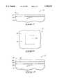
- FIG. 1is a diagrammatic, fragmentary, cross-sectional view of a semiconductive wafer fragment processed according to a method of the present invention.
- FIG. 2is a fragmentary top view of the semiconductor wafer fragment of FIG. 1.
- FIG. 3is a view of the FIG. 1 wafer fragment at a processing step subsequent to that of FIG. 1.
- FIG. 4is a scanning electron microscope (SEM) micrograph of a platinum film produced by CVD of MeCpPt(Me) 3 .
- FIG. 5is a SEM micrograph of a platinum film produced by CVD of MeCpPt(Me) 3 under different conditions than those utilized for forming the film of FIG. 4.
- FIG. 1shows a semiconductor wafer fragment 10 at a preliminary processing step of the present invention.
- Wafer fragment 10comprises a substrate 12.
- Substrate 12can comprise, for example, a monocrystalline silicon wafer lightly doped with a background p-type dopant.
- the term "semiconductive substrate”is defined to mean any construction comprising semiconductive material, including, but not limited to, bulk semiconductive materials such as a semiconductive wafer (either alone or in assemblies comprising other materials thereon), and semiconductive material layers (either alone or in assemblies comprising other materials).
- substraterefers to any supporting structure, including, but not limited to, the semiconductive substrates described above.
- a diffusion region 14is formed within substrate 12 and defines a node location to which electrical connection with a storage node of a capacitor is to be made. Diffusion region 14 can be formed by, for example, implanting a conductivity enhancing dopant into substrate 12.
- Adhesion layer 16is formed over substrate 12 and in electrical contact with diffusion region 14, and a platinum-comprising layer 18 is formed over adhesion layer 16.
- Adhesion layer 16is provided to enhance adhesion of platinum-comprising layer 18 to substrate 12.
- a platinum-comprising layercan be provided directly onto a silicon surface (either the monocrystalline silicon surface of substrate 12, or an intervening amorphous or polycrystalline surface). Such embodiments are less preferred than the shown embodiment due to difficulties of adequately adhering platinum directly to silicon.
- Adhesion layer 16can comprise, for example, at least one of titanium nitride, iridium, rhodium, ruthenium, platinum, palladium, osmium, silver, rhodium/platinum alloy, IrO 2 , RuO 2 , RhO 2 , or OsO 2 .
- Adhesion layer 16can be formed by, for example, chemical vapor deposition, and can be formed to a thickness of, for example, less than 100 ⁇ .
- Platinum-comprising layer 18can comprise, for example, elemental platinum, or a platinum alloy, such as rhodium/platinum alloy. Platinum-comprising layer 18 is provided to have a roughened outer surface 20. Such can be accomplished by chemical vapor deposition of platinum-comprising layer 18 under relatively low temperature conditions, and in the presence of an oxidizing atmosphere. For instance, a platinum-comprising layer 18 formed as follows will comprise a roughened outer surface 20.
- substrate 12is inserted within a CVD reaction chamber.
- An oxidizing gas and a platinum precursorare flowed into the reaction chamber. Platinum is deposited from the platinum precursor over substrate 12 in the presence of the oxidizing gas.
- a temperature within the reaction chamberis maintained at from about 0° C. to less than 300° C. during the depositing, and a pressure within the reactor is preferably maintained at from about 0.5 Torr to about 20 Torr. Suitable control of the temperature and of a relative flow rate of the oxidizing gas to the platinum precursor causes deposited platinum layer 18 to have a roughened outer surface 20.
- the platinum precursoris flowed into the reaction chamber in a carrier gas, such as, for example, a gas known to be generally inert to reaction with platinum precursor materials, such as, for example, helium or argon.
- a carrier gassuch as, for example, a gas known to be generally inert to reaction with platinum precursor materials, such as, for example, helium or argon.
- the platinum precursorcan comprise, for example, at least one of MeCpPtMe 3 , CpPtMe 3 , Pt(acetylacetonate) 2 , Pt(PF 3 ) 4 , Pt(CO) 2 Cl 2 , cis-[PtMe 2 (MeNC) 2 ], or platinum hexafluoroacetylacetonate; wherein Cp is a cyclopentadienyl group and Me is a methyl group.
- the oxidizing gascan comprise, for example, at least one of O 2 , N 2 O, SO 3 , O 3 , H 2 O 2 , or NO x , wherein x has a value of from 1 to 3.
- platinum layer 18comprises a platinum/metal alloy
- at least one other metal precursorcan be flowed into the reaction chamber to deposit the platinum as an alloy of the platinum and the at least one other metal.
- the at least one other metal precursorcan comprise, for example, a precursor of rhodium, iridium, ruthenium, palladium, osmium, and/or silver.
- the oxidizing gascan assist in deposition of platinum from the platinum-comprising precursor by oxidizing carbon from the precursor during deposition of the platinum. Also, the oxidizing gas can influence a deposition rate of a platinum-comprising layer. Specifically, a greater rate of flow of the oxidizing gas relative to the flow of the platinum precursor can lead to faster deposition of the platinum-comprising layer.
- the rate of flow of platinum precursoris influenced by a rate of flow of carrier gas through a liquid organic precursor solution, and by a temperature of the precursor solution.
- a carrier gaswill be flowed through a liquid organic precursor solution at a rate of from about 2 sccm to about 1000 sccm and more preferably at less than or equal to about 30 sccm.
- the oxidizing gaswill be flowed at a flow rate of at least about 50 sccm.
- the organic precursorwill preferably be at a temperature of from about 0° C. to about 100° C., and more preferably from about 30° C. to about 50° C.
- a rate of growth of platinum-comprising layer within the reaction chamberis also influenced by a temperature of the substrate. Specifically, if platinum is deposited under conditions wherein the temperature of the substrate is maintained at from about 220° C. to less than 300° C., the platinum will deposit at a rate of about 600 ⁇ in about 30 seconds. If a temperature of the substrate is reduced to below about 210° C., a rate of deposition of platinum will decrease considerably. It is preferred that a deposition time for a 600 ⁇ thick platinum-comprising layer be less than or equal to about 40 seconds to maintain efficiency of a production process. Accordingly, it is preferred that the temperature of the substrate be maintained at above about 210° C., and preferably at from greater than or equal to about 220° C. during deposition of the platinum-comprising layer within the reaction chamber.
- a temperatureis greater than 300° C. and less than about 350° C.
- a deposited platinum layerwill have a smooth outer surface, rather than a desired roughened outer surface.
- the temperature of the substrateexceeds about 400° C.
- a deposited platinum surfacewill have holes extending to a surface underlying the platinum surface, rather than being a continuous surface overlying a substrate. Accordingly, it is preferred that the temperature of the substrate be well below 400° C., more preferred that the temperature be below 300° C., and even more preferred that the temperature be less than or equal to about 280° C.
- the temperature of the substratewill be maintained at from about 220° C. to about 280° C., whereupon it is found that a platinum layer having a roughened outer surface can be deposited to a thickness of about 600 ⁇ in about 30 seconds.
- Platinum layer 18is preferably deposited to a thickness of at least about 400 ⁇ to avoid having surface anomalies (such as crevices or holes) that extend entirely through layer 18 to an underlying layer, and is preferably deposited to a thickness of at least about 600 ⁇ .
- holes extending entirely through layer 18will be of little or no consequence in semiconductor circuitry ultimately formed from layer 18.
- Such embodimentscan include, for example, embodiments wherein adhesion layer 16 is provided beneath platinum-comprising layer 18. Accordingly, in embodiments wherein platinum layer 18 is provided over an adhesion layer 16, it can be preferred to provide platinum layer 18 to a thickness of less than 400 ⁇ because of space limitations due to the close packing of capacitors.
- platinum layer 18is utilized in forming circuitry having tight spacing requirements it can be preferred to form layer 18 to be relatively thin. For instance, in some capacitor constructions it can be desired to form layer 18 to be less than or equal to about 1000 ⁇ , and more preferred to form layer 18 to be from about 300 ⁇ to about 400 ⁇ to avoid electrical contact between adjacent capacitor structures.
- Layer 18is preferably a continuous layer (defined as a layer without cavities extending therethrough to an underlying layer--such as the underlying layer 16 of FIG. 2) across its entirety. Alternatively, some portion of layer 18 is continuous. For example, consider an application where layer 18 overlies and contacts a conductive layer to form a circuit device comprising both layer 18 and the underlying conductive layer. In such applications, it is generally still desired that a substantial portion of layer 18 be continuous to, for example, maintain a uniform electrical contact between layer 18 and the underlying conductive layer. Such substantial portion will preferably cover a surface area of at least about 4 ⁇ 10 6 square Angstroms. A surface area of about 4 ⁇ 10 6 square Angstroms is illustrated in FIG. 3 as a square 50 having sides of about 2000 Angstroms.
- FIG. 3illustrates an embodiment wherein platinum-comprising layer 18 is incorporated into a capacitor construction 30 as a storage node.
- a dielectric layer 22 and a capacitor electrode 24are provided over platinum-comprising layer 18 to form capacitor construction 30.
- Dielectric layer 22can comprise one or more of silicon oxide or silicon nitride, or it can comprise other dielectric materials, such as, for example, tantalum pentoxide, or BaSrTiO 3 .
- Capacitor electrode 24can comprise, for example, TiN, conductively doped silicon (such as polysilicon), or a metal, such as, for example, platinum.
- capacitor electrode 24comprises platinum
- capacitor electrode 24can be formed by chemical vapor deposition over dielectric layer 22.
- capacitor electrode 24can be formed of platinum with a relatively smooth upper surface, it can be chemical vapor deposited in a reaction chamber with a temperature maintained at above about 300° C. and/or with an oxidizing gas flow rate of less than 50 sccm and a carrier gas flow rate of greater than 30 sccm.
- any platinum comprised by capacitor electrode 24can be in the form of elemental platinum, or an alloy, such as, for example, rhodium/platinum alloy.
- layer 18has a rough outer surface and layers 22 and 24 are conformal to the rough outer surface of layer 18.
- FIGS. 4 and 5illustrate scanning electron microscope (SEM) micrographs of platinum films produced by CVD of MeCpPt(Me) 3 .
- FIG. 4illustrates a surface produced within a reaction chamber in a time of about 6 minutes, wherein a temperature in the chamber was about 215° C., a pressure was about 5 Torr, a flow rate of carrier gas (He, with a pressure at the carrier gas bubbler of about 6 Torr) was about 5 sccm, and a flow rate of oxidizing gas (O 2 ) was about 50 sccm.
- the platinum surface formedcomprises pedestals characteristic of columnar growth. The columnar pedestals terminate in dome-shaped (substantially hemispherical) tops.
- hemispherical topsrather than tops having sharp edges, in forming capacitor constructions or other electronic circuitry from a deposited platinum layer.
- the relatively rounded hemispherical surfacescan create relatively uniform electric fields at the surface of a deposited platinum layer.
- sharp edgescould form loci for high electric fields, and lead to leakage of electric current across the capacitor.
- the platinum layer illustrated in FIG. 4can be referred to as "hemispherical grain" platinum to indicate a structure largely analogous to a material known in the art as hemispherical grain polysilicon.
- the platinum layer of FIG. 4is characterized by columnar pedestals generally having heights greater than or equal to about one-third of a total thickness of the platinum layer. Many of the pedestals shown in FIG. 4 have a height approximately equal to a thickness of the deposited platinum layer. Accordingly, if the deposited platinum layer has a thickness of about 600 ⁇ , the individual pedestals can have a thickness approaching 600 ⁇ . Such is only an approximation to the size of the pedestals as it is found that some of the pedestals will grow from surfaces of other pedestals, and some of the pedestals will grow less vertically than other pedestals.
- An average diameter of the pedestalsis about 200 ⁇ , and the pedestals are generally closely packed (i.e., the pedestals generally touch other pedestals and many pedestals fuse with other pedestals), but the distribution of the pedestals is typically not a close-packed structure (i.e., a structure wherein all the pedestals are tightly packed in, for example, an hexagonal type arrangement to form a maximum number of pedestals on a given surface).
- the columnar growth illustrated in FIG. 4is found not to occur if a temperature within a CVD reaction chamber is above 300° C.
- FIG. 5illustrates a surface produced on a platinum film within a reaction chamber in a time of about 150 seconds, wherein a temperature in the chamber was 300° C., a pressure was about 0.5 Torr, a flow rate of carrier gas (He, with a pressure at the carrier gas bubbler of about 6 Torr) was about 30 sccm, and a flow rate of oxidizing gas (O 2 ) was about 10 sccm.
- the platinum layer deposited under the FIG. 5 conditionshas a much smoother surface-than that deposited under the FIG. 4 conditions.
- FIGS. 4 and 5together evidence that it is possible to control a grain structure of a surface of a chemical vapor deposited platinum layer by controlling process parameters of a chemical vapor deposition reaction chamber.
Landscapes
- Engineering & Computer Science (AREA)
- Power Engineering (AREA)
- Microelectronics & Electronic Packaging (AREA)
- Physics & Mathematics (AREA)
- Condensed Matter Physics & Semiconductors (AREA)
- General Physics & Mathematics (AREA)
- Computer Hardware Design (AREA)
- Manufacturing & Machinery (AREA)
- Chemical & Material Sciences (AREA)
- Chemical Kinetics & Catalysis (AREA)
- General Chemical & Material Sciences (AREA)
- Semiconductor Memories (AREA)
- Chemical Vapour Deposition (AREA)
- Electrodes Of Semiconductors (AREA)
- Semiconductor Integrated Circuits (AREA)
- Fixed Capacitors And Capacitor Manufacturing Machines (AREA)
- Ceramic Capacitors (AREA)
Abstract
Description
Claims (20)
Priority Applications (6)
| Application Number | Priority Date | Filing Date | Title |
|---|---|---|---|
| US09/281,735US5990559A (en) | 1998-08-27 | 1999-03-30 | Circuitry comprising roughened platinum layers, platinum-containing materials, capacitors comprising roughened platinum layers, methods forming roughened layers of platinum, and methods of forming capacitors |
| US09/399,591US6281161B1 (en) | 1998-08-27 | 1999-09-20 | Platinum-containing materials and catalysts |
| US09/421,625US7098503B1 (en) | 1998-08-27 | 1999-10-19 | Circuitry and capacitors comprising roughened platinum layers |
| US10/642,454US7719044B2 (en) | 1998-08-27 | 2003-08-13 | Platinum-containing integrated circuits and capacitor constructions |
| US10/741,256US7060615B2 (en) | 1998-08-27 | 2003-12-17 | Methods of forming roughened layers of platinum |
| US11/212,899US7291920B2 (en) | 1998-08-27 | 2005-08-26 | Semiconductor structures |
Applications Claiming Priority (2)
| Application Number | Priority Date | Filing Date | Title |
|---|---|---|---|
| US09/141,840US6583022B1 (en) | 1998-08-27 | 1998-08-27 | Methods of forming roughened layers of platinum and methods of forming capacitors |
| US09/281,735US5990559A (en) | 1998-08-27 | 1999-03-30 | Circuitry comprising roughened platinum layers, platinum-containing materials, capacitors comprising roughened platinum layers, methods forming roughened layers of platinum, and methods of forming capacitors |
Related Parent Applications (1)
| Application Number | Title | Priority Date | Filing Date |
|---|---|---|---|
| US09/141,840DivisionUS6583022B1 (en) | 1998-08-27 | 1998-08-27 | Methods of forming roughened layers of platinum and methods of forming capacitors |
Related Child Applications (2)
| Application Number | Title | Priority Date | Filing Date |
|---|---|---|---|
| US09/399,591DivisionUS6281161B1 (en) | 1998-08-27 | 1999-09-20 | Platinum-containing materials and catalysts |
| US09/421,625ContinuationUS7098503B1 (en) | 1998-08-27 | 1999-10-19 | Circuitry and capacitors comprising roughened platinum layers |
Publications (1)
| Publication Number | Publication Date |
|---|---|
| US5990559Atrue US5990559A (en) | 1999-11-23 |
Family
ID=22497502
Family Applications (3)
| Application Number | Title | Priority Date | Filing Date |
|---|---|---|---|
| US09/141,840Expired - LifetimeUS6583022B1 (en) | 1998-08-27 | 1998-08-27 | Methods of forming roughened layers of platinum and methods of forming capacitors |
| US09/281,735Expired - LifetimeUS5990559A (en) | 1998-08-27 | 1999-03-30 | Circuitry comprising roughened platinum layers, platinum-containing materials, capacitors comprising roughened platinum layers, methods forming roughened layers of platinum, and methods of forming capacitors |
| US09/399,591Expired - LifetimeUS6281161B1 (en) | 1998-08-27 | 1999-09-20 | Platinum-containing materials and catalysts |
Family Applications Before (1)
| Application Number | Title | Priority Date | Filing Date |
|---|---|---|---|
| US09/141,840Expired - LifetimeUS6583022B1 (en) | 1998-08-27 | 1998-08-27 | Methods of forming roughened layers of platinum and methods of forming capacitors |
Family Applications After (1)
| Application Number | Title | Priority Date | Filing Date |
|---|---|---|---|
| US09/399,591Expired - LifetimeUS6281161B1 (en) | 1998-08-27 | 1999-09-20 | Platinum-containing materials and catalysts |
Country Status (8)
| Country | Link |
|---|---|
| US (3) | US6583022B1 (en) |
| EP (1) | EP1108267B1 (en) |
| JP (1) | JP3550361B2 (en) |
| KR (3) | KR100432177B1 (en) |
| AT (1) | ATE468603T1 (en) |
| AU (1) | AU5589699A (en) |
| DE (1) | DE69942392D1 (en) |
| WO (1) | WO2000013216A1 (en) |
Cited By (28)
| Publication number | Priority date | Publication date | Assignee | Title |
|---|---|---|---|---|
| US6239028B1 (en) | 1998-09-03 | 2001-05-29 | Micron Technology, Inc. | Methods for forming iridium-containing films on substrates |
| US6271131B1 (en) | 1998-08-26 | 2001-08-07 | Micron Technology, Inc. | Methods for forming rhodium-containing layers such as platinum-rhodium barrier layers |
| US6281161B1 (en)* | 1998-08-27 | 2001-08-28 | Micron Technology, Inc. | Platinum-containing materials and catalysts |
| US6284655B1 (en) | 1998-09-03 | 2001-09-04 | Micron Technology, Inc. | Method for producing low carbon/oxygen conductive layers |
| US6323081B1 (en) | 1998-09-03 | 2001-11-27 | Micron Technology, Inc. | Diffusion barrier layers and methods of forming same |
| US6329286B1 (en)* | 1999-04-27 | 2001-12-11 | Micron Technology, Inc. | Methods for forming conformal iridium layers on substrates |
| US6387802B1 (en)* | 1998-12-29 | 2002-05-14 | Micron Technology, Inc. | Nucleation and deposition of Pt films using ultraviolet irradiation |
| WO2001095376A3 (en)* | 2000-06-08 | 2002-06-27 | Micron Technology Inc | Methods for forming rough ruthenium-containing layers and structures/methods using same |
| US20030100183A1 (en)* | 2001-11-28 | 2003-05-29 | Weimin Li | CVD of PtRh with good adhesion and morphology |
| US6642567B1 (en) | 2000-08-31 | 2003-11-04 | Micron Technology, Inc. | Devices containing zirconium-platinum-containing materials and methods for preparing such materials and devices |
| US6660631B1 (en) | 2000-08-31 | 2003-12-09 | Micron Technology, Inc. | Devices containing platinum-iridium films and methods of preparing such films and devices |
| US20030233976A1 (en)* | 2002-06-25 | 2003-12-25 | Marsh Eugene P. | Process for direct deposition of ALD RhO2 |
| US20040036129A1 (en)* | 2002-08-22 | 2004-02-26 | Micron Technology, Inc. | Atomic layer deposition of CMOS gates with variable work functions |
| US20040043578A1 (en)* | 2002-08-29 | 2004-03-04 | Micron Technologies, Inc. | Platinum stuffed with silicon oxide as a diffusion oxygen barrier for semiconductor devices |
| US6737313B1 (en) | 2003-04-16 | 2004-05-18 | Micron Technology, Inc. | Surface treatment of an oxide layer to enhance adhesion of a ruthenium metal layer |
| KR100431820B1 (en)* | 1999-12-28 | 2004-05-20 | 주식회사 하이닉스반도체 | Manufacturing method for storage node of semiconductor device |
| US20040142559A1 (en)* | 2001-08-30 | 2004-07-22 | Weimin Li | Technique for high efficiency metalorganic chemical vapor deposition |
| US20040185636A1 (en)* | 2003-03-18 | 2004-09-23 | Marsh Eugene P. | Method of forming a substrste having a surface comprising at least one of Pt, Pd, Co and Au in at least one of element and alloy forms |
| US20040195688A1 (en)* | 2003-04-02 | 2004-10-07 | Beck Patricia A. | Custom electrodes for molecular memory and logic devices |
| US20040248365A1 (en)* | 2003-06-05 | 2004-12-09 | Heon Lee | Area-efficient stack capacitor |
| US20060045256A1 (en)* | 2004-08-30 | 2006-03-02 | Erdman Joseph L | Scalable call center telecommunications system |
| US20060063363A1 (en)* | 1998-08-27 | 2006-03-23 | Marsh Eugene P | Semiconductor structures |
| US20060292875A1 (en)* | 2002-01-16 | 2006-12-28 | Micron Technology, Inc. | Method for enhancing electrode surface area in DRAM cell capacitors |
| US20070020923A1 (en)* | 2005-07-20 | 2007-01-25 | Micron Technology, Inc. | ALD formed titanium nitride films |
| US7709402B2 (en) | 2006-02-16 | 2010-05-04 | Micron Technology, Inc. | Conductive layers for hafnium silicon oxynitride films |
| US20100255342A1 (en)* | 2002-08-29 | 2010-10-07 | Micron Technology, Inc. | Metal Plating Using Seed Film |
| US20100255653A1 (en)* | 2009-04-07 | 2010-10-07 | Micron Technology, Inc. | Semiconductor processing |
| US10439096B2 (en)* | 2014-11-05 | 2019-10-08 | Osram Opto Semiconductors Gmbh | Method for manufacturing at least one optoelectronic semiconductor chip |
Families Citing this family (11)
| Publication number | Priority date | Publication date | Assignee | Title |
|---|---|---|---|---|
| NL1014696C2 (en)* | 2000-03-20 | 2001-09-28 | Stichting Energie | Manufacture of low-temperature fuel cell electrodes. |
| US7217615B1 (en)* | 2000-08-31 | 2007-05-15 | Micron Technology, Inc. | Capacitor fabrication methods including forming a conductive layer |
| KR100389120B1 (en)* | 2000-09-08 | 2003-06-25 | 한국과학기술원 | Catalyst for Automotive Lean-burn Engine and Process for Preparing the Same |
| KR100434489B1 (en) | 2001-03-22 | 2004-06-05 | 삼성전자주식회사 | Method for depositing ruthenium layer having Ru02 seeding layer |
| US7700454B2 (en) | 2001-07-24 | 2010-04-20 | Samsung Electronics Co., Ltd. | Methods of forming integrated circuit electrodes and capacitors by wrinkling a layer that includes a high percentage of impurities |
| US7105065B2 (en)* | 2002-04-25 | 2006-09-12 | Micron Technology, Inc. | Metal layer forming methods and capacitor electrode forming methods |
| KR100509161B1 (en)* | 2002-07-11 | 2005-08-23 | 주식회사 성진케미칼 | Glass Fiber Pad having A Conductive Rubber Pad Layer and A Polyimide Layer |
| AU2003266998A1 (en)* | 2002-08-23 | 2004-03-11 | Hartmut Presting | Microstructured catalyst body and method for production thereof |
| US7067454B2 (en)* | 2003-04-09 | 2006-06-27 | Honeywell International Inc. | Low cost quick response catalyst system |
| US7440255B2 (en)* | 2003-07-21 | 2008-10-21 | Micron Technology, Inc. | Capacitor constructions and methods of forming |
| US7968488B2 (en) | 2006-04-18 | 2011-06-28 | Southwest Research Institute | Two-dimensional composite particle adapted for use as a catalyst and method of making same |
Citations (2)
| Publication number | Priority date | Publication date | Assignee | Title |
|---|---|---|---|---|
| US5639685A (en)* | 1995-10-06 | 1997-06-17 | Micron Technology, Inc. | Semiconductor processing method of providing a conductively doped layer of hemispherical grain polysilicon |
| US5917213A (en)* | 1997-08-21 | 1999-06-29 | Micron Technology, Inc. | Depletion compensated polysilicon electrodes |
Family Cites Families (25)
| Publication number | Priority date | Publication date | Assignee | Title |
|---|---|---|---|---|
| US3856709A (en) | 1972-04-29 | 1974-12-24 | Getters Spa | Coating a substrate with soft particles |
| US3975304A (en) | 1972-05-03 | 1976-08-17 | S.A.E.S. Getters S.P.A. | Coating a substrate with soft particles |
| US4425261A (en) | 1980-03-24 | 1984-01-10 | Ytkemiska Institutet | Liquid suspension of particles of a metal belonging to the platinum group and a method for the manufacture of such a suspension |
| US4341662A (en) | 1980-04-11 | 1982-07-27 | Pfefferle William C | Method of catalytically coating low porosity ceramic surfaces |
| US4431750A (en) | 1982-05-19 | 1984-02-14 | Phillips Petroleum Company | Platinum group metal catalyst on the surface of a support and a process for preparing same |
| CA1250155A (en) | 1984-07-31 | 1989-02-21 | James A. Ruf | Platinum resistance thermometer |
| US4714693A (en) | 1986-04-03 | 1987-12-22 | Uop Inc. | Method of making a catalyst composition comprising uniform size metal components on carrier |
| US5053917A (en) | 1989-08-30 | 1991-10-01 | Nec Corporation | Thin film capacitor and manufacturing method thereof |
| US5097843A (en) | 1990-04-10 | 1992-03-24 | Siemens-Pacesetter, Inc. | Porous electrode for a pacemaker |
| JP2692402B2 (en) | 1991-02-26 | 1997-12-17 | 日本電気株式会社 | Method for manufacturing semiconductor device |
| US5525570A (en) | 1991-03-09 | 1996-06-11 | Forschungszentrum Julich Gmbh | Process for producing a catalyst layer on a carrier and a catalyst produced therefrom |
| US5208479A (en) | 1992-05-15 | 1993-05-04 | Micron Technology, Inc. | Method of increasing capacitance of polycrystalline silicon devices by surface roughening and polycrystalline silicon devices |
| US5320978A (en)* | 1993-07-30 | 1994-06-14 | The United States Of America As Represented By The Secretary Of The Navy | Selective area platinum film deposition |
| US6052271A (en) | 1994-01-13 | 2000-04-18 | Rohm Co., Ltd. | Ferroelectric capacitor including an iridium oxide layer in the lower electrode |
| US5763286A (en)* | 1994-09-14 | 1998-06-09 | Micron Semiconductor, Inc. | Process for manufacturing a DRAM capacitor having an annularly-grooved, cup-shaped storage-node plate which stores charge on inner and outer surfaces |
| US5555486A (en) | 1994-12-29 | 1996-09-10 | North Carolina State University | Hybrid metal/metal oxide electrodes for ferroelectric capacitors |
| JP3672115B2 (en) | 1995-09-19 | 2005-07-13 | 富士通株式会社 | Thin film forming method and semiconductor device manufacturing method |
| US5874364A (en) | 1995-03-27 | 1999-02-23 | Fujitsu Limited | Thin film deposition method, capacitor device and method for fabricating the same, and semiconductor device and method for fabricating the same |
| US5783716A (en) | 1996-06-28 | 1998-07-21 | Advanced Technology Materials, Inc. | Platinum source compositions for chemical vapor deposition of platinum |
| JP3645338B2 (en)* | 1995-12-11 | 2005-05-11 | 株式会社東芝 | Nonvolatile semiconductor memory device |
| JPH10189909A (en)* | 1996-12-27 | 1998-07-21 | Texas Instr Japan Ltd | Dielectric capacitor, dielectric memory device, and manufacturing method thereof |
| US6054331A (en) | 1997-01-15 | 2000-04-25 | Tong Yang Cement Corporation | Apparatus and methods of depositing a platinum film with anti-oxidizing function over a substrate |
| US5905280A (en) | 1997-02-11 | 1999-05-18 | Micron Technology, Inc. | Capacitor structures, DRAM cell structures, methods of forming capacitors, methods of forming DRAM cells, and integrated circuits incorporating capacitor structures and DRAM cell structures |
| US6010744A (en) | 1997-12-23 | 2000-01-04 | Advanced Technology Materials, Inc. | Method for nucleation controlled chemical vapor deposition of metal oxide ferroelectric thin films |
| US6583022B1 (en)* | 1998-08-27 | 2003-06-24 | Micron Technology, Inc. | Methods of forming roughened layers of platinum and methods of forming capacitors |
- 1998
- 1998-08-27USUS09/141,840patent/US6583022B1/ennot_activeExpired - Lifetime
- 1999
- 1999-03-30USUS09/281,735patent/US5990559A/ennot_activeExpired - Lifetime
- 1999-08-27EPEP99942541Apatent/EP1108267B1/ennot_activeExpired - Lifetime
- 1999-08-27KRKR10-2001-7001364Apatent/KR100432177B1/ennot_activeExpired - Fee Related
- 1999-08-27WOPCT/US1999/019814patent/WO2000013216A1/enactiveIP Right Grant
- 1999-08-27KRKR10-2003-7012178Apatent/KR100451486B1/ennot_activeExpired - Fee Related
- 1999-08-27ATAT99942541Tpatent/ATE468603T1/ennot_activeIP Right Cessation
- 1999-08-27DEDE69942392Tpatent/DE69942392D1/ennot_activeExpired - Lifetime
- 1999-08-27AUAU55896/99Apatent/AU5589699A/ennot_activeAbandoned
- 1999-08-27KRKR10-2003-7012179Apatent/KR20030078967A/ennot_activeCeased
- 1999-08-27JPJP2000568109Apatent/JP3550361B2/ennot_activeExpired - Fee Related
- 1999-09-20USUS09/399,591patent/US6281161B1/ennot_activeExpired - Lifetime
Patent Citations (2)
| Publication number | Priority date | Publication date | Assignee | Title |
|---|---|---|---|---|
| US5639685A (en)* | 1995-10-06 | 1997-06-17 | Micron Technology, Inc. | Semiconductor processing method of providing a conductively doped layer of hemispherical grain polysilicon |
| US5917213A (en)* | 1997-08-21 | 1999-06-29 | Micron Technology, Inc. | Depletion compensated polysilicon electrodes |
Non-Patent Citations (4)
| Title |
|---|
| Ju Hong Kwan et al.; Characterization of Pt Thin Films Deposited by Metallorganic Chemical Vapor Deposition for Ferroelectric Bottom Electrodes ; J. Electrochem. Soc., vol. 144, No. 8, Aug. 1997; pp. 2848 2854.* |
| Ju-Hong Kwan et al.; "Characterization of Pt Thin Films Deposited by Metallorganic Chemical Vapor Deposition for Ferroelectric Bottom Electrodes"; J. Electrochem. Soc., vol. 144, No. 8, Aug. 1997; pp. 2848-2854. |
| M. Ino et al.; "Rugged surface polycrystalline silicon film deposition and its application in a stacked dynamic random access memory capacitor electrode"; J. Vac. Sci. Technol. B 14(2), Mar./Apr. 1996; pp. 751-756. |
| M. Ino et al.; Rugged surface polycrystalline silicon film deposition and its application in a stacked dynamic random access memory capacitor electrode ; J. Vac. Sci. Technol. B 14(2), Mar./Apr. 1996; pp. 751 756.* |
Cited By (89)
| Publication number | Priority date | Publication date | Assignee | Title |
|---|---|---|---|---|
| US7393785B2 (en) | 1998-08-26 | 2008-07-01 | Micron Technology, Inc. | Methods and apparatus for forming rhodium-containing layers |
| US6271131B1 (en) | 1998-08-26 | 2001-08-07 | Micron Technology, Inc. | Methods for forming rhodium-containing layers such as platinum-rhodium barrier layers |
| US20040147086A1 (en)* | 1998-08-26 | 2004-07-29 | Micron Technology, Inc. | Methods and apparatus for forming rhodium-containing layers |
| US20050260823A9 (en)* | 1998-08-26 | 2005-11-24 | Micron Technology, Inc. | Methods and apparatus for forming rhodium-containing layers |
| US6690055B1 (en) | 1998-08-26 | 2004-02-10 | Micron Technology, Inc. | Devices containing platinum-rhodium layers and methods |
| US7226861B2 (en) | 1998-08-26 | 2007-06-05 | Micron Technology, Inc. | Methods and apparatus for forming rhodium-containing layers |
| US7060615B2 (en) | 1998-08-27 | 2006-06-13 | Micron Technology, Inc. | Methods of forming roughened layers of platinum |
| US7719044B2 (en) | 1998-08-27 | 2010-05-18 | Micron Technology, Inc. | Platinum-containing integrated circuits and capacitor constructions |
| US6281161B1 (en)* | 1998-08-27 | 2001-08-28 | Micron Technology, Inc. | Platinum-containing materials and catalysts |
| US20060063363A1 (en)* | 1998-08-27 | 2006-03-23 | Marsh Eugene P | Semiconductor structures |
| US7098503B1 (en)* | 1998-08-27 | 2006-08-29 | Micron Technology, Inc. | Circuitry and capacitors comprising roughened platinum layers |
| US7291920B2 (en)* | 1998-08-27 | 2007-11-06 | Micron Technology, Inc. | Semiconductor structures |
| US20020146902A1 (en)* | 1998-09-03 | 2002-10-10 | Micron Technology, Inc. | Chemical vapor deposition apparatus |
| US6284655B1 (en) | 1998-09-03 | 2001-09-04 | Micron Technology, Inc. | Method for producing low carbon/oxygen conductive layers |
| US6239028B1 (en) | 1998-09-03 | 2001-05-29 | Micron Technology, Inc. | Methods for forming iridium-containing films on substrates |
| US6403414B2 (en) | 1998-09-03 | 2002-06-11 | Micron Technology, Inc. | Method for producing low carbon/oxygen conductive layers |
| US6495458B2 (en) | 1998-09-03 | 2002-12-17 | Micron Technology, Inc. | Method for producing low carbon/oxygen conductive layers |
| US6323081B1 (en) | 1998-09-03 | 2001-11-27 | Micron Technology, Inc. | Diffusion barrier layers and methods of forming same |
| US6323511B1 (en) | 1998-09-03 | 2001-11-27 | Micron Technology, Inc. | Structures including low carbon/oxygen conductive layers |
| US6426292B2 (en) | 1998-09-03 | 2002-07-30 | Micron Technology, Inc. | Methods for forming iridium and platinum containing films on substrates |
| US20060014367A1 (en)* | 1998-12-29 | 2006-01-19 | Micron Technology, Inc. | Nucleation and deposition of platinum group metal films using ultraviolet irradiation |
| US6387802B1 (en)* | 1998-12-29 | 2002-05-14 | Micron Technology, Inc. | Nucleation and deposition of Pt films using ultraviolet irradiation |
| US6329286B1 (en)* | 1999-04-27 | 2001-12-11 | Micron Technology, Inc. | Methods for forming conformal iridium layers on substrates |
| KR100431820B1 (en)* | 1999-12-28 | 2004-05-20 | 주식회사 하이닉스반도체 | Manufacturing method for storage node of semiconductor device |
| US7144810B2 (en) | 2000-06-08 | 2006-12-05 | Micron Technology, Inc. | Methods for forming rough ruthenium-containing layers and structures/methods using same |
| US6897160B2 (en) | 2000-06-08 | 2005-05-24 | Micron Technology, Inc. | Methods for forming rough ruthenium-containing layers and structures/methods using same |
| WO2001095376A3 (en)* | 2000-06-08 | 2002-06-27 | Micron Technology Inc | Methods for forming rough ruthenium-containing layers and structures/methods using same |
| US6429127B1 (en)* | 2000-06-08 | 2002-08-06 | Micron Technology, Inc. | Methods for forming rough ruthenium-containing layers and structures/methods using same |
| US20050208741A1 (en)* | 2000-06-08 | 2005-09-22 | Micron Technology, Inc. | Methods for forming rough ruthenium-containing layers and structures/methods using same |
| US6784504B2 (en) | 2000-06-08 | 2004-08-31 | Micron Technology, Inc. | Methods for forming rough ruthenium-containing layers and structures/methods using same |
| US6900107B2 (en) | 2000-08-31 | 2005-05-31 | Micron Technology, Inc. | Devices containing platinum-iridium films and methods of preparing such films and devices |
| US20040048467A1 (en)* | 2000-08-31 | 2004-03-11 | Micron Technologies, Inc. | Devices containing platinum-iridium films and methods of preparing such films and devices |
| US20050101131A9 (en)* | 2000-08-31 | 2005-05-12 | Micron Technology, Inc. | Devices containing zirconium-platinum-containing materials and methods for preparing such materials and devices |
| US6642567B1 (en) | 2000-08-31 | 2003-11-04 | Micron Technology, Inc. | Devices containing zirconium-platinum-containing materials and methods for preparing such materials and devices |
| US6660631B1 (en) | 2000-08-31 | 2003-12-09 | Micron Technology, Inc. | Devices containing platinum-iridium films and methods of preparing such films and devices |
| US20050006689A1 (en)* | 2000-08-31 | 2005-01-13 | Micron Technology, Inc. | Devices containing platinum-iridium films and methods of preparing such films and devices |
| US7217970B2 (en) | 2000-08-31 | 2007-05-15 | Micron Technology, Inc. | Devices containing platinum-iridium films and methods of preparing such films and devices |
| US20060051963A1 (en)* | 2000-08-31 | 2006-03-09 | Micron Technology, Inc. | Devices containing zirconium-platinum-containing materials and methods for preparing such materials and devices |
| US20040067642A1 (en)* | 2000-08-31 | 2004-04-08 | Micron Technology, Inc. | Devices containing zirconium-platinum-containing materials and methods for preparing such materials and devices |
| US6946395B2 (en) | 2000-08-31 | 2005-09-20 | Micron Technology, Inc. | Devices containing zirconium-platinum-containing materials and methods for preparing such materials and devices |
| US7214618B2 (en) | 2001-08-30 | 2007-05-08 | Micron Technology, Inc. | Technique for high efficiency metalorganic chemical vapor deposition |
| US20040142559A1 (en)* | 2001-08-30 | 2004-07-22 | Weimin Li | Technique for high efficiency metalorganic chemical vapor deposition |
| US20050223978A1 (en)* | 2001-08-30 | 2005-10-13 | Weimin Li | Technique for high efficiency metalorganic chemical vapor deposition |
| US6921710B2 (en)* | 2001-08-30 | 2005-07-26 | Micron Technology, Inc. | Technique for high efficiency metalorganic chemical vapor deposition |
| US20040147103A1 (en)* | 2001-08-30 | 2004-07-29 | Weimin Li | Technique for high efficiency metaloganic chemical vapor deposition |
| US20050066895A1 (en)* | 2001-11-28 | 2005-03-31 | Weimin Li | CVD of PtRh with good adhesion and morphology |
| US20030100183A1 (en)* | 2001-11-28 | 2003-05-29 | Weimin Li | CVD of PtRh with good adhesion and morphology |
| US6918960B2 (en)* | 2001-11-28 | 2005-07-19 | Micron Technology, Inc. | CVD of PtRh with good adhesion and morphology |
| US7573121B2 (en) | 2002-01-16 | 2009-08-11 | Micron Technology, Inc. | Method for enhancing electrode surface area in DRAM cell capacitors |
| EP1610379A3 (en)* | 2002-01-16 | 2007-03-07 | Micron Technology, Inc. | Dram cell capacitors having enhancing electrode surface area and method of their manufacture |
| US20060292875A1 (en)* | 2002-01-16 | 2006-12-28 | Micron Technology, Inc. | Method for enhancing electrode surface area in DRAM cell capacitors |
| US20070048955A1 (en)* | 2002-01-16 | 2007-03-01 | Micron Technology, Inc. | Method for enhancing electrode surface area in DRAM cell capacitors |
| US7642157B2 (en) | 2002-01-16 | 2010-01-05 | Micron Technology, Inc. | Method for enhancing electrode surface area in DRAM cell capacitors |
| US6881260B2 (en) | 2002-06-25 | 2005-04-19 | Micron Technology, Inc. | Process for direct deposition of ALD RhO2 |
| US20030233976A1 (en)* | 2002-06-25 | 2003-12-25 | Marsh Eugene P. | Process for direct deposition of ALD RhO2 |
| US20040036129A1 (en)* | 2002-08-22 | 2004-02-26 | Micron Technology, Inc. | Atomic layer deposition of CMOS gates with variable work functions |
| US20100255342A1 (en)* | 2002-08-29 | 2010-10-07 | Micron Technology, Inc. | Metal Plating Using Seed Film |
| US20050082587A1 (en)* | 2002-08-29 | 2005-04-21 | Micron Technology, Inc. | Platinum stuffed with silicon oxide as a diffusion oxygen barrier for semiconductor devices |
| US20040043578A1 (en)* | 2002-08-29 | 2004-03-04 | Micron Technologies, Inc. | Platinum stuffed with silicon oxide as a diffusion oxygen barrier for semiconductor devices |
| US6830983B2 (en) | 2002-08-29 | 2004-12-14 | Micron Technology, Inc. | Method of making an oxygen diffusion barrier for semiconductor devices using platinum, rhodium, or iridium stuffed with silicon oxide |
| US8431240B2 (en)* | 2002-08-29 | 2013-04-30 | Micron Technology, Inc. | Metal plating using seed film |
| US7157783B2 (en) | 2002-08-29 | 2007-01-02 | Micron Technology, Inc. | Platinum stuffed with silicon oxide as a diffusion oxygen barrier for semiconductor devices |
| US8734957B2 (en) | 2002-08-29 | 2014-05-27 | Micron Technology, Inc. | Metal plating using seed film |
| US7271071B2 (en) | 2003-03-18 | 2007-09-18 | Micron Technology, Inc. | Method of forming a catalytic surface comprising at least one of Pt, Pd, Co and Au in at least one of elemental and alloy forms |
| US6884691B2 (en) | 2003-03-18 | 2005-04-26 | Micron Technology, Inc. | Method of forming a substrate having a surface comprising at least one of Pt, Pd, Co and Au in at least one of elemental and alloy forms |
| US20050191437A1 (en)* | 2003-03-18 | 2005-09-01 | Marsh Eugene P. | Method of forming a catalytic surface comprising at least one of Pt, Pd, Co and Au in at least one of elemental and alloy forms |
| US20040185636A1 (en)* | 2003-03-18 | 2004-09-23 | Marsh Eugene P. | Method of forming a substrste having a surface comprising at least one of Pt, Pd, Co and Au in at least one of element and alloy forms |
| US20050164412A1 (en)* | 2003-04-02 | 2005-07-28 | Beck Patricia A. | Custom electrodes for molecular memory and logic devices |
| US20050032203A1 (en)* | 2003-04-02 | 2005-02-10 | Beck Patricia A. | Custom electrodes for molecular memory and logic devices |
| US6855647B2 (en)* | 2003-04-02 | 2005-02-15 | Hewlett-Packard Development Company, L.P. | Custom electrodes for molecular memory and logic devices |
| US20040195688A1 (en)* | 2003-04-02 | 2004-10-07 | Beck Patricia A. | Custom electrodes for molecular memory and logic devices |
| US7282408B2 (en) | 2003-04-16 | 2007-10-16 | Micron Technology, Inc. | Surface treatment of an oxide layer to enhance adhesion of a ruthenium metal layer |
| US20040214354A1 (en)* | 2003-04-16 | 2004-10-28 | Marsh Eugene P. | Surface treatment of an oxide layer to enhance adhesion of a ruthenium metal layer |
| US6737313B1 (en) | 2003-04-16 | 2004-05-18 | Micron Technology, Inc. | Surface treatment of an oxide layer to enhance adhesion of a ruthenium metal layer |
| US6838339B2 (en)* | 2003-06-05 | 2005-01-04 | Infineon Technologies Ag | Area-efficient stack capacitor |
| US20040248365A1 (en)* | 2003-06-05 | 2004-12-09 | Heon Lee | Area-efficient stack capacitor |
| US20060045256A1 (en)* | 2004-08-30 | 2006-03-02 | Erdman Joseph L | Scalable call center telecommunications system |
| US20070200243A1 (en)* | 2005-07-20 | 2007-08-30 | Micron Technology, Inc. | Ald formed titanium nitride films |
| US20070020923A1 (en)* | 2005-07-20 | 2007-01-25 | Micron Technology, Inc. | ALD formed titanium nitride films |
| US7473637B2 (en) | 2005-07-20 | 2009-01-06 | Micron Technology, Inc. | ALD formed titanium nitride films |
| US8633110B2 (en) | 2005-07-20 | 2014-01-21 | Micron Technology, Inc. | Titanium nitride films |
| US8058729B2 (en) | 2005-07-20 | 2011-11-15 | Micron Technology, Inc. | Titanium nitride films |
| US7709402B2 (en) | 2006-02-16 | 2010-05-04 | Micron Technology, Inc. | Conductive layers for hafnium silicon oxynitride films |
| US8067794B2 (en) | 2006-02-16 | 2011-11-29 | Micron Technology, Inc. | Conductive layers for hafnium silicon oxynitride films |
| US8785312B2 (en) | 2006-02-16 | 2014-07-22 | Micron Technology, Inc. | Conductive layers for hafnium silicon oxynitride |
| US8455296B2 (en) | 2009-04-07 | 2013-06-04 | Micron Technology, Inc. | Semiconductor processing |
| US8003521B2 (en) | 2009-04-07 | 2011-08-23 | Micron Technology, Inc. | Semiconductor processing |
| US20100255653A1 (en)* | 2009-04-07 | 2010-10-07 | Micron Technology, Inc. | Semiconductor processing |
| US10439096B2 (en)* | 2014-11-05 | 2019-10-08 | Osram Opto Semiconductors Gmbh | Method for manufacturing at least one optoelectronic semiconductor chip |
Also Published As
| Publication number | Publication date |
|---|---|
| EP1108267B1 (en) | 2010-05-19 |
| JP3550361B2 (en) | 2004-08-04 |
| ATE468603T1 (en) | 2010-06-15 |
| US6281161B1 (en) | 2001-08-28 |
| AU5589699A (en) | 2000-03-21 |
| DE69942392D1 (en) | 2010-07-01 |
| KR20030078967A (en) | 2003-10-08 |
| WO2000013216A1 (en) | 2000-03-09 |
| EP1108267A1 (en) | 2001-06-20 |
| KR100432177B1 (en) | 2004-05-22 |
| KR20010053624A (en) | 2001-06-25 |
| JP2002524655A (en) | 2002-08-06 |
| US6583022B1 (en) | 2003-06-24 |
| KR100451486B1 (en) | 2004-10-08 |
| KR20030083748A (en) | 2003-10-30 |
Similar Documents
| Publication | Publication Date | Title |
|---|---|---|
| US5990559A (en) | Circuitry comprising roughened platinum layers, platinum-containing materials, capacitors comprising roughened platinum layers, methods forming roughened layers of platinum, and methods of forming capacitors | |
| US6740554B2 (en) | Methods to form rhodium-rich oxygen barriers | |
| US6764895B2 (en) | Process for fabricating RuSixOy-containing adhesion layers | |
| US5733816A (en) | Method for depositing a tungsten layer on silicon | |
| EP1114449B1 (en) | Method for forming a capacitor with a ruthenium silicide diffusion barrier layer | |
| KR100355585B1 (en) | Thin film capacitor | |
| US7291920B2 (en) | Semiconductor structures | |
| US6734100B2 (en) | Method of forming ruthenium thin film using plasma enhanced process | |
| KR100503961B1 (en) | Method of manufacturing a capacitor | |
| US6054332A (en) | Method for fabricating capacitor of semiconductor memory device | |
| KR100493707B1 (en) | Ruthenium Thin Film Formation Method | |
| US6033534A (en) | Method for producing an Al-containing layer with a planar surface on a substrate having hole structures with a high aspect ratio in the surface |
Legal Events
| Date | Code | Title | Description |
|---|---|---|---|
| STCF | Information on status: patent grant | Free format text:PATENTED CASE | |
| CC | Certificate of correction | ||
| FPAY | Fee payment | Year of fee payment:4 | |
| FPAY | Fee payment | Year of fee payment:8 | |
| FPAY | Fee payment | Year of fee payment:12 | |
| AS | Assignment | Owner name:U.S. BANK NATIONAL ASSOCIATION, AS COLLATERAL AGENT, CALIFORNIA Free format text:SECURITY INTEREST;ASSIGNOR:MICRON TECHNOLOGY, INC.;REEL/FRAME:038669/0001 Effective date:20160426 Owner name:U.S. BANK NATIONAL ASSOCIATION, AS COLLATERAL AGEN Free format text:SECURITY INTEREST;ASSIGNOR:MICRON TECHNOLOGY, INC.;REEL/FRAME:038669/0001 Effective date:20160426 | |
| AS | Assignment | Owner name:MORGAN STANLEY SENIOR FUNDING, INC., AS COLLATERAL AGENT, MARYLAND Free format text:PATENT SECURITY AGREEMENT;ASSIGNOR:MICRON TECHNOLOGY, INC.;REEL/FRAME:038954/0001 Effective date:20160426 Owner name:MORGAN STANLEY SENIOR FUNDING, INC., AS COLLATERAL Free format text:PATENT SECURITY AGREEMENT;ASSIGNOR:MICRON TECHNOLOGY, INC.;REEL/FRAME:038954/0001 Effective date:20160426 | |
| AS | Assignment | Owner name:U.S. BANK NATIONAL ASSOCIATION, AS COLLATERAL AGENT, CALIFORNIA Free format text:CORRECTIVE ASSIGNMENT TO CORRECT THE REPLACE ERRONEOUSLY FILED PATENT #7358718 WITH THE CORRECT PATENT #7358178 PREVIOUSLY RECORDED ON REEL 038669 FRAME 0001. ASSIGNOR(S) HEREBY CONFIRMS THE SECURITY INTEREST;ASSIGNOR:MICRON TECHNOLOGY, INC.;REEL/FRAME:043079/0001 Effective date:20160426 Owner name:U.S. BANK NATIONAL ASSOCIATION, AS COLLATERAL AGEN Free format text:CORRECTIVE ASSIGNMENT TO CORRECT THE REPLACE ERRONEOUSLY FILED PATENT #7358718 WITH THE CORRECT PATENT #7358178 PREVIOUSLY RECORDED ON REEL 038669 FRAME 0001. ASSIGNOR(S) HEREBY CONFIRMS THE SECURITY INTEREST;ASSIGNOR:MICRON TECHNOLOGY, INC.;REEL/FRAME:043079/0001 Effective date:20160426 | |
| AS | Assignment | Owner name:JPMORGAN CHASE BANK, N.A., AS COLLATERAL AGENT, ILLINOIS Free format text:SECURITY INTEREST;ASSIGNORS:MICRON TECHNOLOGY, INC.;MICRON SEMICONDUCTOR PRODUCTS, INC.;REEL/FRAME:047540/0001 Effective date:20180703 Owner name:JPMORGAN CHASE BANK, N.A., AS COLLATERAL AGENT, IL Free format text:SECURITY INTEREST;ASSIGNORS:MICRON TECHNOLOGY, INC.;MICRON SEMICONDUCTOR PRODUCTS, INC.;REEL/FRAME:047540/0001 Effective date:20180703 | |
| AS | Assignment | Owner name:MICRON TECHNOLOGY, INC., IDAHO Free format text:RELEASE BY SECURED PARTY;ASSIGNOR:U.S. BANK NATIONAL ASSOCIATION, AS COLLATERAL AGENT;REEL/FRAME:047243/0001 Effective date:20180629 | |
| AS | Assignment | Owner name:MICRON TECHNOLOGY, INC., IDAHO Free format text:RELEASE BY SECURED PARTY;ASSIGNOR:MORGAN STANLEY SENIOR FUNDING, INC., AS COLLATERAL AGENT;REEL/FRAME:050937/0001 Effective date:20190731 | |
| AS | Assignment | Owner name:MICRON SEMICONDUCTOR PRODUCTS, INC., IDAHO Free format text:RELEASE BY SECURED PARTY;ASSIGNOR:JPMORGAN CHASE BANK, N.A., AS COLLATERAL AGENT;REEL/FRAME:051028/0001 Effective date:20190731 Owner name:MICRON TECHNOLOGY, INC., IDAHO Free format text:RELEASE BY SECURED PARTY;ASSIGNOR:JPMORGAN CHASE BANK, N.A., AS COLLATERAL AGENT;REEL/FRAME:051028/0001 Effective date:20190731 |