US5989972A - Capacitor in a semiconductor configuration and process for its production - Google Patents
Capacitor in a semiconductor configuration and process for its productionDownload PDFInfo
- Publication number
- US5989972A US5989972AUS08/685,847US68584796AUS5989972AUS 5989972 AUS5989972 AUS 5989972AUS 68584796 AUS68584796 AUS 68584796AUS 5989972 AUS5989972 AUS 5989972A
- Authority
- US
- United States
- Prior art keywords
- doped
- layer
- highly
- conductive
- process according
- Prior art date
- Legal status (The legal status is an assumption and is not a legal conclusion. Google has not performed a legal analysis and makes no representation as to the accuracy of the status listed.)
- Expired - Lifetime
Links
- 239000003990capacitorSubstances0.000titleclaimsabstractdescription87
- 239000004065semiconductorSubstances0.000titleclaimsabstractdescription22
- 238000000034methodMethods0.000titleclaimsdescription41
- 238000004519manufacturing processMethods0.000titleabstractdescription7
- 238000005530etchingMethods0.000claimsabstractdescription32
- 230000002093peripheral effectEffects0.000claimsabstractdescription10
- 239000004020conductorSubstances0.000claimsabstractdescription8
- 239000000758substrateSubstances0.000claimsdescription28
- 238000000151depositionMethods0.000claimsdescription20
- YCIMNLLNPGFGHC-UHFFFAOYSA-NcatecholChemical compoundOC1=CC=CC=C1OYCIMNLLNPGFGHC-UHFFFAOYSA-N0.000claimsdescription12
- 239000000463materialSubstances0.000claimsdescription10
- VYPSYNLAJGMNEJ-UHFFFAOYSA-NSilicium dioxideChemical compoundO=[Si]=OVYPSYNLAJGMNEJ-UHFFFAOYSA-N0.000claimsdescription9
- 238000002513implantationMethods0.000claimsdescription9
- 229910052814silicon oxideInorganic materials0.000claimsdescription9
- -1boron fluoride ionsChemical class0.000claimsdescription7
- 230000008021depositionEffects0.000claimsdescription7
- PIICEJLVQHRZGT-UHFFFAOYSA-NEthylenediamineChemical compoundNCCNPIICEJLVQHRZGT-UHFFFAOYSA-N0.000claimsdescription6
- 229910052581Si3N4Inorganic materials0.000claimsdescription6
- HQVNEWCFYHHQES-UHFFFAOYSA-Nsilicon nitrideChemical compoundN12[Si]34N5[Si]62N3[Si]51N64HQVNEWCFYHHQES-UHFFFAOYSA-N0.000claimsdescription6
- KWYUFKZDYYNOTN-UHFFFAOYSA-MPotassium hydroxideChemical compound[OH-].[K+]KWYUFKZDYYNOTN-UHFFFAOYSA-M0.000claimsdescription5
- 238000005304joiningMethods0.000claimsdescription4
- 150000004767nitridesChemical class0.000claimsdescription3
- 150000002500ionsChemical class0.000claimsdescription2
- 229910015900BF3Inorganic materials0.000claims1
- 229910021420polycrystalline siliconInorganic materials0.000description22
- 229920005591polysiliconPolymers0.000description22
- 210000004027cellAnatomy0.000description13
- 239000000243solutionSubstances0.000description9
- 229910052796boronInorganic materials0.000description7
- XUIMIQQOPSSXEZ-UHFFFAOYSA-NSiliconChemical compound[Si]XUIMIQQOPSSXEZ-UHFFFAOYSA-N0.000description6
- 229910052710siliconInorganic materials0.000description6
- 239000010703siliconSubstances0.000description6
- 239000002019doping agentSubstances0.000description4
- 239000012212insulatorSubstances0.000description4
- WFKWXMTUELFFGS-UHFFFAOYSA-NtungstenChemical compound[W]WFKWXMTUELFFGS-UHFFFAOYSA-N0.000description4
- 229910052721tungstenInorganic materials0.000description4
- 239000010937tungstenSubstances0.000description4
- RTAQQCXQSZGOHL-UHFFFAOYSA-NTitaniumChemical compound[Ti]RTAQQCXQSZGOHL-UHFFFAOYSA-N0.000description3
- NRTOMJZYCJJWKI-UHFFFAOYSA-NTitanium nitrideChemical compound[Ti]#NNRTOMJZYCJJWKI-UHFFFAOYSA-N0.000description3
- 238000002955isolationMethods0.000description3
- 229910052751metalInorganic materials0.000description3
- 239000002184metalSubstances0.000description3
- 238000004151rapid thermal annealingMethods0.000description3
- 229910052715tantalumInorganic materials0.000description3
- GUVRBAGPIYLISA-UHFFFAOYSA-Ntantalum atomChemical compound[Ta]GUVRBAGPIYLISA-UHFFFAOYSA-N0.000description3
- 239000010936titaniumSubstances0.000description3
- 229910052719titaniumInorganic materials0.000description3
- ZOXJGFHDIHLPTG-UHFFFAOYSA-NBoronChemical compound[B]ZOXJGFHDIHLPTG-UHFFFAOYSA-N0.000description2
- 238000009792diffusion processMethods0.000description2
- 239000011521glassSubstances0.000description2
- 238000004518low pressure chemical vapour depositionMethods0.000description2
- 229910021332silicideInorganic materials0.000description2
- FVBUAEGBCNSCDD-UHFFFAOYSA-Nsilicide(4-)Chemical compound[Si-4]FVBUAEGBCNSCDD-UHFFFAOYSA-N0.000description2
- 241000071092CandelabrumSpecies0.000description1
- 239000012670alkaline solutionSubstances0.000description1
- 230000015572biosynthetic processEffects0.000description1
- 239000005380borophosphosilicate glassSubstances0.000description1
- 238000010276constructionMethods0.000description1
- 229910021419crystalline siliconInorganic materials0.000description1
- 230000003247decreasing effectEffects0.000description1
- 230000000694effectsEffects0.000description1
- 238000005516engineering processMethods0.000description1
- 239000007943implantSubstances0.000description1
- 238000011065in-situ storageMethods0.000description1
- 230000010354integrationEffects0.000description1
- 238000012986modificationMethods0.000description1
- 230000004048modificationEffects0.000description1
- 238000001451molecular beam epitaxyMethods0.000description1
- 230000003647oxidationEffects0.000description1
- 238000007254oxidation reactionMethods0.000description1
- 238000012856packingMethods0.000description1
- 238000005498polishingMethods0.000description1
- 238000003860storageMethods0.000description1
Images


Classifications
- H—ELECTRICITY
- H10—SEMICONDUCTOR DEVICES; ELECTRIC SOLID-STATE DEVICES NOT OTHERWISE PROVIDED FOR
- H10B—ELECTRONIC MEMORY DEVICES
- H10B12/00—Dynamic random access memory [DRAM] devices
- H10B12/01—Manufacture or treatment
- H10B12/02—Manufacture or treatment for one transistor one-capacitor [1T-1C] memory cells
- H10B12/03—Making the capacitor or connections thereto
- H10B12/033—Making the capacitor or connections thereto the capacitor extending over the transistor
- H—ELECTRICITY
- H10—SEMICONDUCTOR DEVICES; ELECTRIC SOLID-STATE DEVICES NOT OTHERWISE PROVIDED FOR
- H10B—ELECTRONIC MEMORY DEVICES
- H10B12/00—Dynamic random access memory [DRAM] devices
- H10B12/30—DRAM devices comprising one-transistor - one-capacitor [1T-1C] memory cells
- H10B12/31—DRAM devices comprising one-transistor - one-capacitor [1T-1C] memory cells having a storage electrode stacked over the transistor
- H10B12/318—DRAM devices comprising one-transistor - one-capacitor [1T-1C] memory cells having a storage electrode stacked over the transistor the storage electrode having multiple segments
Definitions
- the inventionrelates to a capacitor in a semiconductor configuration, in particular a DRAM configuration, having an electrode structure which contains a plurality of spaced-apart elements that are electrically connected to one another by a connecting structure, a capacitor dielectric, and a counterelectrode.
- the inventionalso relates to a process for producing a capacitor in a semiconductor configuration.
- a multiplicity of integrated circuitsrequire capacitors. Examples, besides the typical one of a dynamic memory cell, are analog/digital or digital/analog converters and filter circuits. Provisions are needed for reducing the intrinsically great amount of space that a capacitor requires, particularly with the miniaturization of structures involved in the increased scale of integration or since chip area has to be economized upon.
- a typical examplemay be considered to be the dynamic semiconductor memory, in which the required area of the usually used single-transistor memory cell is reduced from one memory generation to another with increasing memory density. At the same time, the minimum capacitance of the memory capacitor must be preserved.
- a single-transistor memory cellincludes a readout transistor and a capacitor.
- the informationthat is the electric charge, stored in the capacitor can be read out through a bit line.
- the memory capacitormust have a minimum capacitance in order to provide reliable storage of the charge and simultaneous capability of distinguishing the read-out information.
- the lower limit for the capacitance of the memory capacitoris currently considered to be 20 fF.
- the thickness of the dielectricIn order to attain that capacitor capacitance, the thickness of the dielectric must be as small as possible and the area of the capacitor as large as possible.
- a further option for increasing the capacitance with an unchanged changed or reduced space requirement for the capacitoris to construct the capacitor as a stacked capacitor.
- a polysilicon structurefor instance a crown structure or a cylinder, is formed that is contacted with the substrate.
- the polysilicon structureforms a memory node that is provided with the capacitor dielectric and the capacitor plate or so-called cell plate. That concept has the advantage of being compatible with a logic process.
- the free space above the substrate surfaceis used for the capacitor.
- the entire cell surfacecan be covered with the polysilicon structure, as long as the structures of adjacent memory cells are isolated from one another.
- Known configurations along those linesare the fin stacked capacitor and the crown stacked capacitor.
- the stacked capacitorincludes a polysilicon structure with a plurality of polysilicon layers, stacked substantially parallel to each other and joined together through at least one lateral support.
- the lateral supportis produced with the aid of a polysilicon layer that is subsequently etched back, so that a substantially upright land remains that joins the polysilicon layers which are stacked one above the other.
- the structureis formed by alternatingly depositing polysilicon layers and silicon oxide layers, which are etchable selectively to them, on the surface of the substrate, by structuring those layers, by producing the lateral supports on at least one side of the structure, and by selective etching out of the silicon oxide layers.
- the polysilicon structuresare arsenic-doped.
- silicon oxideis formed by thermal oxidation as the capacitor dielectric, over which the cell plate of doped polysilicon is deposited.
- variously rapidly etching isolation layersare applied over a polysilicon layer. The isolation layers are then structured and etched, producing a support framework.
- doped polysiliconis deposited and then a silicon nitride layer, followed by the formation of the cell plate.
- a capacitor in a semiconductor configurationin particular a DRAM configuration, comprising an electrode structure containing a plurality of spaced-apart elements and a connecting structure electrically connecting the elements to one another, the connecting structure and the elements of the electrode structure all being formed of p-conductive material with a dopant concentration of at least 10 20 cm -3 ; a capacitor dielectric; and a counterelectrode.
- the thickness of the capacitoris less with a horizontal configuration, and the width of the capacitor is less in a vertical configuration, than in the known capacitors.
- the capacitorcan be used in DRAM semiconductor configurations, since for the requisite minimum cell capacitance of 20 fF it is slight in thickness and occupies only a slight amount of surface area. It can be estimated that with such a capacitor the memory capacities of future generations of DRAMs, which make even more stringent demands in terms of their space requirement, will be realized. All that is needed for this purpose is to increase the number of layers and reduce the area of one layer. It is also possible to reduce the thickness or width of the capacitor by reducing the layer thickness and the dielectric thickness.
- the capacitoradditionally has the advantage of enabling its electrode structure, in p-channel transistors, to be joined directly to the drain of the transistor with the aid of a contact hole.
- contacting the electrode structure with other circuit elementsare also possible.
- contacting of the electrode structure to the drain of the transistorcan be carried out through an intermediate metal layer, for instance of tantalum, titanium or titanium nitride, or a silicide layer or a filling of contact of holes, for instance with tungsten.
- a process for producing a capacitor in a semiconductor configurationwhich comprises producing a base layer including a highly-doped p-conductive layer, on a surface of a substrate configuration; applying a layer sequence of one low-doped and one highly-doped p-conductive alternatingly layer, on a surface of the highly-doped p-conductive layer; structuring the layer sequence by an anisotropic etching, forming at least one opening extending as far as the base layer; producing a highly-doped p-conductive zone joining the layer sequence, at least in a peripheral region of the opening; selectively etching the low-doped p-conductive layers of the layer sequence to the highly-doped p-conductive layer sequence; conformally depositing a capacitor dielectric; and conformally depositing a conductive layer over the capacitor dielectric.
- the process of the inventionhas the substantial advantage over known methods of requiring fewer process steps, without having to make sacrifices in other respects.
- the capacitor in the semiconductor configurationhas an electrode structure that includes a plurality of spaced-apart elements, which are electrically connected to one another by a connecting structure.
- the elements of the electrode structure and the associated connecting structureare all of p- doped material with a doping >10 20 cm -3 .
- the elements of the electrode structureare disposed generally flatly in stacked fashion or side by side.
- the connecting structureextends, on at least one edge, in a direction crosswise to the surface of the elements.
- the elements of the electrode structuremay be cup-shaped and interested in one another.
- the connecting structureis joined inside the cup-shaped region to a substrate of the capacitor configuration and to the bottom part or bottom parts of the elements.
- the connecting structureis constructed as a rodlike support elements, centrally inside the cup-shaped electrode structure.
- a base layeris produced that includes a p + layer, over which a layer sequence including alternatingly one low-doped and one highly-doped p-conductive layer is then applied.
- the layer sequenceis etched anisotropically in such a way that an opening is formed which extends at least as far as the p + layer of the base layer.
- a p + -conductive zoneis subsequently produced, which joins the layer sequence.
- the low-doped p-conductive layers of the layer sequenceare etched selectively to the p + layers, the dielectric is deposited, and a counterelectrode is formed.
- the base layeris produced in such a way that it contains only one p + layer, or one p + layer with an underlying layer of oxide and/or nitride.
- the p + zone in the openingis produced by oblique implantation of ions, that is boron ions, or by applying a p + -conductive material.
- ionsthat is boron ions
- a p + -conductive materialThe important factor in this case is that the layer sequence not be covered completely by a p + zone, to allow the etchant to attack the low-doped p- material in the ensuing selective etching.
- the selective etchingis carried out with the aid of an alkaline etchant, for instance an ethylene diamine pyrocatechol solution or a potassium hydroxide solution.
- an alkaline etchantfor instance an ethylene diamine pyrocatechol solution or a potassium hydroxide solution.
- a dielectricis applied, for instance an ONO dielectric, and then a conductive material is conformally deposited as a counterelectrode.
- the base layeris produced on a planarized surface of an insulator. If a contact hole to an underlying terminal surface is provided in the insulator, then this contact hole can likewise be filled up with the p + material of the base layer. In addition to this vertical contacting of the electrode structure, contacting through lateral terminals is also possible.
- the base layer and subsequently the electrode structurecan on the other hand be produced in a trench of an isolation layer or a silicon layer.
- a silicon oxide and/or a silicon nitride layeris provided underneath the p + partial layer of the base layer.
- the production of the capacitoris based on the knowledge that the etching rate of p + -doped silicon is extremely low as compared with low-doped silicon in alkaline etching solutions.
- H. Seidel et alentitled: Anisotropic Etching of Crystalline Silicon in Alkaline Solutions, J. Electrochem. Soc., Vol. 137, No. 11, November 1990, pp. 3626-3632
- the etching rate of p-doped silicon in an ethylene diamine pyrocatechol solutionis constant down to a concentration of 10 19 cm -3 , and then drops off sharply. At a concentration of 2 ⁇ 10 20 cm -3 , the etching rate is then only less than 1/1000 the etching rate at 10 19 cm -3 .
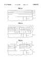
- FIGS. 1a-1fare fragmentary, diagrammatic, cross-sectional views illustrating a production of a first exemplary embodiment of a capacitor
- FIG. 2is a fragmentary, cross-sectional view of a second exemplary embodiment of a capacitor
- FIGS. 3a and 3bare plan views of possible geometrical configurations.
- FIGS. 4a-4care fragmentary, cross-sectional views illustrating a production through a third exemplary embodiment of a capacitor.
- FIG. 1athere is seen a substrate configuration that has an insulating layer 1 on its surface.
- Other elements of a semiconductor configurationsuch as transistors, may be disposed underneath the insulating layer.
- a contact hole 2is provided, flush with the surface, and the hole is filled with a metallizing material.
- Tungsten, tantalum, titanium, titanium nitride, or doped polysiliconmay be provided as the filling material. In the case of n-doped polysilicon, it is necessary to silicize this material, so that a metal intermediate layer appears at the surface.
- a glass layersuch as BPSG, may be provided as the insulating layer 1 of the substrate configuration. It has the advantage of a plane surface from liquefication of the glass. However, it is also possible to provide an insulating layer that is planarized through the use of a polishing step, such as CMP.
- a base layer 3is produced, which in the exemplary embodiment is a highly-doped p-conductive layer.
- the magnitude of the dopingdepends on the choice of the etching solution to be used layer and should be selected in such a way that the etching rate is extraordinarily low. For instance, for an ethylene diamine pyrocatechol solution, it is expedient to choose a boron concentration >10 20 cm -3 .
- the thickness of the base layermay be 300 nm, for instance.
- a layer sequenceis applied including alternatingly one p- and one p + layer.
- the highly doped layers 5 and 7are doped in the same way as the highly-doped p-conductive layer of the base layer.
- the low-doped p-conductive layers 4 and 6have doping that enables a high etching rate with respect to the selectively acting etchant.
- the boron dopant in the ethylene diamine pyrocatechol solution described first aboveis approximately 10 19 cm -3 or less.
- the layer thicknessesare chosen in such a way that the low-doped p-conductive layers are thicker than the highly-doped p-conductive layers.
- the p- layersare 30 nm thick, and the p + layers 5 and 7 are 10 nm thick.
- the layers 3-7are conformally deposited. Examples of possible deposition methods are low-pressure chemical vapor deposition, particularly hot-wall or cold-wall LPCVD, or molecular beam epitaxy.
- the layer sequencemay be applied in situ in one and the same reactor. This requires setting different process parameters for the p--doped layers 4 and 6 and the p + -doped polysilicon layers 3, 5 and 7, respectively.
- a non-illustrated maskis produced with the aid of which the layer sequence 3-7 is etched anisotropically, forming one or more openings 8.
- KOHis one possible etchant.
- the openings 8are etched through to the insulating layer of the substrate configuration 1. This creates separate islands, in each of which one capacitor can be produced. However, it is not necessary in every case to etch the openings as far as the p + -conductive layer of the base layer. If the base layer 3 is not etched all the way through, a large-area capacitor configuration is created.
- the structuring of the polysilicon layer sequenceis carried out in such a way that the stacks are round or polygonal in plan view, as seen in FIGS. 3a and 3b.
- a highly-doped p-conductive zoneis created in a peripheral region of the opening 8 and joins the layer sequence 3-7.
- an oblique implantation of BF 2 ionsis carried out, for instance at an angle of 8° from the vertical.
- the effect of the implantationis that the peripheral region of the opening that lies under the bombardment of the boron ions has a limited highly doped zone located in the low-doped p-conductive layers 4 and 6. This high doping is equivalent to the doping of the remaining p + polysilicon layers.
- a temperature stepis provided, in order to assure that the implanted boron ions will be activated, or in other words will occupy the corresponding spaces in the lattice of the polysilicon layer 4 and 6. This requires that no diffusion from the highly doped zones into the low-doped zones occur.
- the temperature stepcan preferably be carried out with the aid of an RTA (rapid thermal annealing) process.
- the selected temperatureis approximately 850 to 900° C.
- FIG. 1cshows the structure that has arisen after the temperature step.
- the oblique implantation of boron ions into the openings 8has created a p + zone 9 in the peripheral region of each opening. This zone joins together the p + layers 3, 5 and 7.
- the p + zonestake the form of a letter "E" pointing to the left.
- the originally created layer sequences 3-7are obtained, so that the low-doped layers 4 and 6 point freely toward the opening.
- the zones 9extend with decreasing thickness over a certain portion of the circumference of the stack.
- a rectangular stackit can be accomplished that only one side of the stack or two sides of the stack are peripherally p + -doped.
- the zones 9are present either on only one side of the stack or angularly cover two sides of the stack.
- the diameter of a stack shaped in this way, that is its width,is approximately 1 ⁇ m.
- FIGS. 3a and 3bshow examples for the embodiment of the structured, doped stacks of FIG. 1c. In each case the direction with which the implantation has been carried out is indicated. In the examples shown in FIGS. 3a and 3b, a very stable structure for the capacitor to be produced is attained.
- the configurationis selectively etched isotropically with an alkaline etchant.
- Ethylene diamine pyrocatecholis, for instance, possible as the etching solution.
- the alkaline etching solutionshave the property that the low-doped p-conductive layers are etched more strongly than the p + -doped layers, with a selectivity of 100:1 to 1000:1.
- the result after the etching operationis a structure of FIG. 1d, in which only the p + -doped regions then remain, joined together in such a way that a support structure is the result. This structure is marked with reference numeral 10.
- the capacitor dielectricis conformally deposited.
- the dielectricmay be formed of silicon oxide and/or silicon nitride.
- an ONO dielectric layeris provided, which includes a first silicon oxide layer, a silicon nitride layer, and a second silicon oxide layer.
- the overall layer thickness of the capacitor dielectricis intended to be approximately 10 nm. However, the chosen thickness of the capacitor dielectric may be less, for instance 3 nm for higher capacitances to be produced.
- a counterelectrode 12 of the capacitoris produced, for instance, in the form of p + -doped polysilicon, over a capacitor dielectric 11, by conformal deposition.
- the same methods that have already been used to produce the layer sequencecan be considered for this deposition method.
- the counterelectrode 12can be optionally structured and contacted with typical methods in semiconductor technology.
- FIG. 2shows a second exemplary embodiment of the capacitor, in which the capacitor is intended as a memory capacitor in a DRAM semiconductor configuration.
- a substrate configuration beneath the insulating layer 1includes the selection transistors of the memory capacity. Isolated regions are formed in a substrate 20 with the aid of field oxide zones 21.
- An isolated regionincludes two selection transistors 30 and 40, respectively, which have one common source zone 22. Extending on both sides of the source zone 22 is a channel region, which is controlled by a gate 32 and 42, respectively, as a word line, that is isolated on all sides in cross section.
- the transistorseach have respective drain zones 31 and 41.
- Each drain of a memory cellwhich is formed by one selection transistor and one capacitor, is joined to the electrode structure of a capacitor through a contact hole in the insulating layer.
- the drain 31 of the transistor 30is connected to an electrode 33 of a first capacitor K1
- the drain 41 of the transistor 40is connected to an electrode 43 of a second capacitor K2.
- the electrode structure 33 and 43in contrast to the exemplary embodiment of FIG. 1, is produced in such a way that in the substrate layer 1, the contact holes 2 are first produced in the form of self-adjusted overlapping contacts to the drain zones of the respective transistor, and after that the p + -doped base layer is produced by conformal deposition, with which the contact hole is filled.
- the p + -doped base layeris produced by conformal deposition, with which the contact hole is filled.
- the source and drain zones 22, 31 and 41are provided as p + -doped zones, corresponding to p-channel selection transistors.
- the contact hole 2In n-channel selection transistors, the contact hole 2 must have an intermediate layer with a metallically conductive material, such as tungsten, tantalum, titanium, titanium nitride, or a silicide.
- Word lines 23 for the next memory cellsare disposed above the field oxide region 21.
- the word lines 23, 32 and 42preferably include highly doped polysilicon or polycide.
- the source zone 22is made to contact a bit line 50, which is made of tungsten or polycide.
- all of the capacitorshave one common counterelectrode 34, the so-called cell plate.
- FIG. 4shows a further exemplary embodiment of the capacitor, which in this case is constructed as a cup-shaped configuration.
- an insulator layer 60is formed on a substrate 1 with a contact hole 2 that is filled, for instance, with metal.
- the insulator layer 60is then structured, creating an opening down to the substrate layer 1 or the filled contact hole 2.
- a base layer 61 of highly-doped p-conductive polysiliconis formed in the manner already described, and then over that a layer sequence is applied, which alternatingly includes a low-doped and a highly-doped p-conductive layer.
- the low-doped layersare designated by reference numerals 62, 64 and 66 and the highly-doped layers by reference numerals 63 and 65.
- the result initiallyis a structure in which the layers 61-66 rest in one another in cup-like fashion and in which the layers applied later in the group are smaller at the bottom and on the periphery than the layers applied first.
- an opening 70is created centrally in the layer sequence, reaching as far as the base layer 61.
- the layer sequenceis laid bare in the bottom region, as is seen in FIG. 4a.
- the opening 70is at least partially filled with a highly-doped p-conductive material. This can be carried out as for the layers 63 and 65. If there is a sufficiently large opening in comparison with the edge height of the layers, an oblique implantation can alternatively be selected.
- a mask and one or more successive implantation stepsit is possible through the use of a mask and one or more successive implantation steps to dope the region, defined by the mask opening, on the bottom of the layer sequence with p + atoms.
- a plurality of implantation stepsare provided in such a way that the maximum doping in each case is located in a p- layer region. This creates a p + support, defined by the mask opening, in the bottom region.
- the p + -doped zoneshave a dopant concentration of at least 10 20 cm -3
- the low-doped p- zones 62, 64 and 66have a dopant concentration of at most 10 19 cm -3
- a temperature stepmay be appended, for instance an RTA step, so that no diffusion from the p + -doped layers can occur.
- the structureis etched selectively, isotropically, in an alkaline etching solution. In this process the p + -doped layers remain, while the p--doped layers are etched out.
- the selectivity of the etching processis sufficiently high to produce a support structure as in FIG. 4b, which looks something like a candelabrum.
- the central highly-doped p- conductive zone 70is produced in such a way that the opening 70 in the bottom region of the layer sequence is filled completely.
- the depositionis carried out conformally by the deposition methods already mentioned, followed by structuring.
- a zone 71therefore joins together the layer sequence 72, shown in FIG. 4b, in the bottom region of the layer sequence.
- a dielectric 73for instance in the form of an ONO dielectric
- a counterelectrode 74for instance of p + -doped polysilicon
- the base layer in the contact hole 2is deposit as well by conformal deposition, if desired. It is also possible to place a capacitor of the type shown in FIG. 4 in a silicon substrate and to join the electrode structure at the edge of the trench to a semiconductor configuration, for instance a selection transistor of a DRAM configuration.
- the counterelectrode 74may be constructed as a continuous cell plate, as in known trench capacitors. If the capacitor in a silicon substrate is disposed as a trench capacitor, it suffices, for a p-substrate, to produce the base zone through the use of higher doping of the trench region.
- the highly-doped p-conductive layer of the base layer 61is isolated from the substrate by an insulating layer. Such a layer may be formed of silicon oxide and/or silicon nitride.
Landscapes
- Engineering & Computer Science (AREA)
- Manufacturing & Machinery (AREA)
- Semiconductor Memories (AREA)
- Semiconductor Integrated Circuits (AREA)
Abstract
Description
Claims (21)
Applications Claiming Priority (2)
| Application Number | Priority Date | Filing Date | Title |
|---|---|---|---|
| DE19527023ADE19527023C1 (en) | 1995-07-24 | 1995-07-24 | Method of manufacturing a capacitor in a semiconductor device |
| DE19527023 | 1995-07-24 |
Publications (1)
| Publication Number | Publication Date |
|---|---|
| US5989972Atrue US5989972A (en) | 1999-11-23 |
Family
ID=7767656
Family Applications (1)
| Application Number | Title | Priority Date | Filing Date |
|---|---|---|---|
| US08/685,847Expired - LifetimeUS5989972A (en) | 1995-07-24 | 1996-07-24 | Capacitor in a semiconductor configuration and process for its production |
Country Status (7)
| Country | Link |
|---|---|
| US (1) | US5989972A (en) |
| EP (1) | EP0756326B1 (en) |
| JP (1) | JP3955344B2 (en) |
| KR (1) | KR100425399B1 (en) |
| DE (2) | DE19527023C1 (en) |
| SG (1) | SG43381A1 (en) |
| TW (1) | TW315507B (en) |
Cited By (7)
| Publication number | Priority date | Publication date | Assignee | Title |
|---|---|---|---|---|
| WO2002001607A2 (en) | 2000-06-23 | 2002-01-03 | Infineon Technologies North America Corp. | Method of producing trench capacitor buried strap |
| WO2002011200A1 (en)* | 2000-07-31 | 2002-02-07 | Infineon Technologies Ag | Semiconductor memory cell arrangement and method for producing the same |
| WO2002001567A3 (en)* | 2000-06-23 | 2002-02-25 | Infineon Technologies Corp | Structure and process for 6f<2> trench capacitor dram cell with vertical mosfet and 3f bitline pitch |
| US6368970B1 (en)* | 2000-08-24 | 2002-04-09 | Infineon Technologies Ag | Semiconductor configuration and corresponding production process |
| FR2819633A1 (en)* | 2001-01-18 | 2002-07-19 | St Microelectronics Sa | Method for the integration of DRAM memory by providing a cell architecture that augments the density of integration |
| US20070013071A1 (en)* | 2005-06-24 | 2007-01-18 | International Business Machines Corporation | Probing pads in kerf area for wafer testing |
| US20140096552A1 (en)* | 2011-03-09 | 2014-04-10 | Georg Foesel | Expansion valve for a vapour compression system with reversible fluid flow |
Families Citing this family (8)
| Publication number | Priority date | Publication date | Assignee | Title |
|---|---|---|---|---|
| JPH11297960A (en)* | 1998-04-16 | 1999-10-29 | Mitsubishi Electric Corp | Semiconductor device and manufacturing method thereof |
| US5744833A (en)* | 1996-08-16 | 1998-04-28 | United Microelectronics Corporation | Semiconductor memory device having tree-type capacitor |
| US6309975B1 (en)* | 1997-03-14 | 2001-10-30 | Micron Technology, Inc. | Methods of making implanted structures |
| DE19842704C2 (en)* | 1998-09-17 | 2002-03-28 | Infineon Technologies Ag | Manufacturing process for a capacitor with a high epsilon dielectric or a ferroelectric according to the fin stack principle using a negative mold |
| DE19842684C1 (en)* | 1998-09-17 | 1999-11-04 | Siemens Ag | Integrated circuit high-permittivity capacitor arranged on support structure in semiconductor arrangement e.g. for DRAM circuit or ADC |
| DE19842682A1 (en)* | 1998-09-17 | 2000-04-06 | Siemens Ag | Capacitor with a high-e dielectric or a ferro-electrical according to the fin stack principle and manufacturing process |
| US6426253B1 (en)* | 2000-05-23 | 2002-07-30 | Infineon Technologies A G | Method of forming a vertically oriented device in an integrated circuit |
| TWI306303B (en)* | 2006-08-23 | 2009-02-11 | Promos Technologies Inc | Method for preparing memory structure |
Citations (16)
| Publication number | Priority date | Publication date | Assignee | Title |
|---|---|---|---|---|
| EP0295709A2 (en)* | 1987-06-17 | 1988-12-21 | Fujitsu Limited | Dynamic random access memory device and method of producing the same |
| EP0415530A1 (en)* | 1989-07-05 | 1991-03-06 | Fujitsu Limited | Semiconductor memory device having stacked capacitor and method of producing the same |
| US5084405A (en)* | 1991-06-07 | 1992-01-28 | Micron Technology, Inc. | Process to fabricate a double ring stacked cell structure |
| EP0484088A1 (en)* | 1990-10-29 | 1992-05-06 | Nec Corporation | Stacked capacitor DRAM cell |
| US5126280A (en)* | 1991-02-08 | 1992-06-30 | Micron Technology, Inc. | Stacked multi-poly spacers with double cell plate capacitor |
| US5150276A (en)* | 1992-01-24 | 1992-09-22 | Micron Technology, Inc. | Method of fabricating a vertical parallel cell capacitor having a storage node capacitor plate comprising a center fin effecting electrical communication between itself and parallel annular rings |
| US5153813A (en)* | 1991-10-31 | 1992-10-06 | International Business Machines Corporation | High area capacitor formation using dry etching |
| US5155657A (en)* | 1991-10-31 | 1992-10-13 | International Business Machines Corporation | High area capacitor formation using material dependent etching |
| US5160987A (en)* | 1989-10-26 | 1992-11-03 | International Business Machines Corporation | Three-dimensional semiconductor structures formed from planar layers |
| EP0513988A1 (en)* | 1991-04-05 | 1992-11-19 | Nec Corporation | Method of producing capacitive element for dram |
| US5206787A (en)* | 1991-04-01 | 1993-04-27 | Fujitsu Limited | Capacitor and method of fabricating same |
| US5214296A (en)* | 1991-03-11 | 1993-05-25 | Matsushita Electric Industrial Co., Ltd. | Thin-film semiconductor device and method of fabricating the same |
| US5240871A (en)* | 1991-09-06 | 1993-08-31 | Micron Technology, Inc. | Corrugated storage contact capacitor and method for forming a corrugated storage contact capacitor |
| DE4307575A1 (en)* | 1992-03-12 | 1993-09-23 | Mitsubishi Electric Corp | Semiconductor device with improved operational speed - comprises substrate, foreign atom region, first layer with insulating film and second layer |
| US5412237A (en)* | 1992-03-12 | 1995-05-02 | Mitsubishi Denki Kabushiki Kaisha | Semiconductor device with improved element isolation and operation rate |
| GB2285338A (en)* | 1993-12-29 | 1995-07-05 | Hyundai Electronics Ind | Method for fabricating capacitor |
Family Cites Families (1)
| Publication number | Priority date | Publication date | Assignee | Title |
|---|---|---|---|---|
| JPH069154A (en)* | 1992-04-23 | 1994-01-18 | Teijin Seiki Co Ltd | Thread switching winder |
- 1995
- 1995-07-24DEDE19527023Apatent/DE19527023C1/ennot_activeExpired - Fee Related
- 1996
- 1996-07-02TWTW085107986Apatent/TW315507B/zhactive
- 1996-07-04SGSG1996010212Apatent/SG43381A1/enunknown
- 1996-07-18DEDE59608481Tpatent/DE59608481D1/ennot_activeExpired - Fee Related
- 1996-07-18EPEP96111674Apatent/EP0756326B1/ennot_activeExpired - Lifetime
- 1996-07-24JPJP21217296Apatent/JP3955344B2/ennot_activeExpired - Fee Related
- 1996-07-24USUS08/685,847patent/US5989972A/ennot_activeExpired - Lifetime
- 1996-07-24KRKR1019960029913Apatent/KR100425399B1/ennot_activeExpired - Fee Related
Patent Citations (18)
| Publication number | Priority date | Publication date | Assignee | Title |
|---|---|---|---|---|
| EP0295709A2 (en)* | 1987-06-17 | 1988-12-21 | Fujitsu Limited | Dynamic random access memory device and method of producing the same |
| EP0415530A1 (en)* | 1989-07-05 | 1991-03-06 | Fujitsu Limited | Semiconductor memory device having stacked capacitor and method of producing the same |
| US5126810A (en)* | 1989-07-05 | 1992-06-30 | Fujitsu Limited | Semiconductor memory device having stacked capacitor |
| US5160987A (en)* | 1989-10-26 | 1992-11-03 | International Business Machines Corporation | Three-dimensional semiconductor structures formed from planar layers |
| EP0484088A1 (en)* | 1990-10-29 | 1992-05-06 | Nec Corporation | Stacked capacitor DRAM cell |
| US5126280A (en)* | 1991-02-08 | 1992-06-30 | Micron Technology, Inc. | Stacked multi-poly spacers with double cell plate capacitor |
| US5214296A (en)* | 1991-03-11 | 1993-05-25 | Matsushita Electric Industrial Co., Ltd. | Thin-film semiconductor device and method of fabricating the same |
| US5206787A (en)* | 1991-04-01 | 1993-04-27 | Fujitsu Limited | Capacitor and method of fabricating same |
| EP0513988A1 (en)* | 1991-04-05 | 1992-11-19 | Nec Corporation | Method of producing capacitive element for dram |
| US5084405A (en)* | 1991-06-07 | 1992-01-28 | Micron Technology, Inc. | Process to fabricate a double ring stacked cell structure |
| US5240871A (en)* | 1991-09-06 | 1993-08-31 | Micron Technology, Inc. | Corrugated storage contact capacitor and method for forming a corrugated storage contact capacitor |
| US5153813A (en)* | 1991-10-31 | 1992-10-06 | International Business Machines Corporation | High area capacitor formation using dry etching |
| US5155657A (en)* | 1991-10-31 | 1992-10-13 | International Business Machines Corporation | High area capacitor formation using material dependent etching |
| US5150276A (en)* | 1992-01-24 | 1992-09-22 | Micron Technology, Inc. | Method of fabricating a vertical parallel cell capacitor having a storage node capacitor plate comprising a center fin effecting electrical communication between itself and parallel annular rings |
| DE4301690A1 (en)* | 1992-01-24 | 1993-07-29 | Micron Technology Inc | |
| DE4307575A1 (en)* | 1992-03-12 | 1993-09-23 | Mitsubishi Electric Corp | Semiconductor device with improved operational speed - comprises substrate, foreign atom region, first layer with insulating film and second layer |
| US5412237A (en)* | 1992-03-12 | 1995-05-02 | Mitsubishi Denki Kabushiki Kaisha | Semiconductor device with improved element isolation and operation rate |
| GB2285338A (en)* | 1993-12-29 | 1995-07-05 | Hyundai Electronics Ind | Method for fabricating capacitor |
Non-Patent Citations (5)
| Title |
|---|
| "Anisotropic Etching of Crystalline Silicon in Alkaline Solutions" (Seidel et al.), J. Electrochem. Soc., vol. 137, No. 11, Nov. 1990, pp. 3626-3632. |
| "Stacked Capacitor DRAM Cell with Vertical FINS (VF-STC)", Technical Disclosure Bulletin, vol. 33, No. 2, Jul. 1990, pp. 245-247. |
| Anisotropic Etching of Crystalline Silicon in Alkaline Solutions (Seidel et al.), J. Electrochem. Soc., vol. 137, No. 11, Nov. 1990, pp. 3626 3632.* |
| Patent Abstracts of Japan No. 60009154 (Masahiro et al.), dated Jan. 18, 1985.* |
| Stacked Capacitor DRAM Cell with Vertical FINS (VF STC) , Technical Disclosure Bulletin, vol. 33, No. 2, Jul. 1990, pp. 245 247.* |
Cited By (13)
| Publication number | Priority date | Publication date | Assignee | Title |
|---|---|---|---|---|
| WO2002001567A3 (en)* | 2000-06-23 | 2002-02-25 | Infineon Technologies Corp | Structure and process for 6f<2> trench capacitor dram cell with vertical mosfet and 3f bitline pitch |
| WO2002001607A2 (en) | 2000-06-23 | 2002-01-03 | Infineon Technologies North America Corp. | Method of producing trench capacitor buried strap |
| WO2002001607A3 (en)* | 2000-06-23 | 2002-05-23 | Infineon Technologies Corp | Method of producing trench capacitor buried strap |
| KR100822079B1 (en) | 2000-06-23 | 2008-04-15 | 인터내셔널 비지네스 머신즈 코포레이션 | Single cotton buried strap |
| US6853023B2 (en) | 2000-07-31 | 2005-02-08 | Infineon Technologies Ag | Semiconductor memory cell configuration and a method for producing the configuration |
| WO2002011200A1 (en)* | 2000-07-31 | 2002-02-07 | Infineon Technologies Ag | Semiconductor memory cell arrangement and method for producing the same |
| US20030169629A1 (en)* | 2000-07-31 | 2003-09-11 | Bernd Goebel | Semiconductor memory cell configuration and a method for producing the configuration |
| US6368970B1 (en)* | 2000-08-24 | 2002-04-09 | Infineon Technologies Ag | Semiconductor configuration and corresponding production process |
| US6759304B2 (en) | 2001-01-18 | 2004-07-06 | Stmicroelectronics Sa | DRAM memory integration method |
| FR2819633A1 (en)* | 2001-01-18 | 2002-07-19 | St Microelectronics Sa | Method for the integration of DRAM memory by providing a cell architecture that augments the density of integration |
| US20070013071A1 (en)* | 2005-06-24 | 2007-01-18 | International Business Machines Corporation | Probing pads in kerf area for wafer testing |
| US7482675B2 (en)* | 2005-06-24 | 2009-01-27 | International Business Machines Corporation | Probing pads in kerf area for wafer testing |
| US20140096552A1 (en)* | 2011-03-09 | 2014-04-10 | Georg Foesel | Expansion valve for a vapour compression system with reversible fluid flow |
Also Published As
| Publication number | Publication date |
|---|---|
| JP3955344B2 (en) | 2007-08-08 |
| DE59608481D1 (en) | 2002-01-31 |
| DE19527023C1 (en) | 1997-02-27 |
| KR100425399B1 (en) | 2004-06-26 |
| SG43381A1 (en) | 1997-10-17 |
| EP0756326B1 (en) | 2001-12-19 |
| TW315507B (en) | 1997-09-11 |
| EP0756326A1 (en) | 1997-01-29 |
| JPH0936333A (en) | 1997-02-07 |
Similar Documents
| Publication | Publication Date | Title |
|---|---|---|
| US5460994A (en) | Semiconductor device having vertical conduction transistors and cylindrical cell gates | |
| US5959322A (en) | Isolated SOI memory structure with vertically formed transistor and storage capacitor in a substrate | |
| US6262449B1 (en) | High density dynamic random access memory cell structure having a polysilicon pillar capacitor | |
| US5792689A (en) | Method for manufacturing double-crown capacitors self-aligned to node contacts on dynamic random access memory | |
| EP0430404B1 (en) | Method of manufacturing a capacitor for a DRAM cell | |
| US5885864A (en) | Method for forming compact memory cell using vertical devices | |
| US5005103A (en) | Method of manufacturing folded capacitors in semiconductor and folded capacitors fabricated thereby | |
| US6242809B1 (en) | Integrated circuit memory devices including titanium nitride bit lines | |
| US5989972A (en) | Capacitor in a semiconductor configuration and process for its production | |
| US5766994A (en) | Dynamic random access memory fabrication method having stacked capacitors with increased capacitance | |
| US6630380B1 (en) | Method for making three-dimensional metal-insulator-metal capacitors for dynamic random access memory (DRAM) and ferroelectric random access memory (FERAM) | |
| US20020055222A1 (en) | Semiconductor memory device having self-aligned contact and fabricating method thereof | |
| US5795804A (en) | Method of fabricating a stack/trench capacitor for a dynamic random access memory (DRAM) | |
| US6563161B2 (en) | Memory-storage node and the method of fabricating the same | |
| US5104821A (en) | Method for fabricating stacked capacitors in a DRAM cell | |
| US5807782A (en) | Method of manufacturing a stacked capacitor having a fin-shaped storage electrode on a dynamic random access memory cell | |
| CN113437070B (en) | Semiconductor device and method for forming the same | |
| US5879987A (en) | Method of fabricating dynamic random access memory having a stacked capacitor | |
| US6271099B1 (en) | Method for forming a capacitor of a DRAM cell | |
| CN215183962U (en) | Semiconductor device with a plurality of semiconductor chips | |
| US5783848A (en) | Memory cell | |
| US6171924B1 (en) | Method of fabricating a dynamic random access memory capacitor | |
| US6232648B1 (en) | Extended self-aligned crown-shaped rugged capacitor for high density DRAM cells | |
| US6391714B2 (en) | Method for fabricating a capacitor in a semiconductor memory device | |
| US5719419A (en) | Capacitor structure for a dynamic random access memory cell |
Legal Events
| Date | Code | Title | Description |
|---|---|---|---|
| AS | Assignment | Owner name:SIEMENS AKTIENGESELLSCHAFT, GERMANY Free format text:ASSIGNMENT OF ASSIGNORS INTEREST;ASSIGNORS:WIDMANN, DIETRICH;MELZNER, HANNO;HOENLEIN, WOLFGANG;REEL/FRAME:010304/0426;SIGNING DATES FROM 19960809 TO 19960906 | |
| STCF | Information on status: patent grant | Free format text:PATENTED CASE | |
| FEPP | Fee payment procedure | Free format text:PAYOR NUMBER ASSIGNED (ORIGINAL EVENT CODE: ASPN); ENTITY STATUS OF PATENT OWNER: LARGE ENTITY | |
| FPAY | Fee payment | Year of fee payment:4 | |
| FPAY | Fee payment | Year of fee payment:8 | |
| AS | Assignment | Owner name:INFINEON TECHNOLOGIES AG,GERMANY Free format text:ASSIGNMENT OF ASSIGNORS INTEREST;ASSIGNOR:SIEMENS AKTIENGESELLSCHAFT;REEL/FRAME:024120/0587 Effective date:19990331 | |
| XAS | Not any more in us assignment database | Free format text:ASSIGNMENT OF ASSIGNORS INTEREST;ASSIGNOR:SIEMENS AKTIENGESELLSCHAFT;REEL/FRAME:023957/0001 | |
| AS | Assignment | Owner name:QIMONDA AG,GERMANY Free format text:ASSIGNMENT OF ASSIGNORS INTEREST;ASSIGNOR:INFINEON TECHNOLOGIES AG;REEL/FRAME:024016/0001 Effective date:20060425 | |
| FPAY | Fee payment | Year of fee payment:12 | |
| AS | Assignment | Owner name:INFINEON TECHNOLOGIES AG, GERMANY Free format text:ASSIGNMENT OF ASSIGNORS INTEREST;ASSIGNOR:QIMONDA AG;REEL/FRAME:035623/0001 Effective date:20141009 | |
| AS | Assignment | Owner name:POLARIS INNOVATIONS LIMITED, IRELAND Free format text:ASSIGNMENT OF ASSIGNORS INTEREST;ASSIGNOR:INFINEON TECHNOLOGIES AG;REEL/FRAME:036201/0432 Effective date:20150708 |