US5989936A - Microelectronic assembly fabrication with terminal formation from a conductive layer - Google Patents
Microelectronic assembly fabrication with terminal formation from a conductive layerDownload PDFInfo
- Publication number
- US5989936A US5989936AUS08/989,312US98931297AUS5989936AUS 5989936 AUS5989936 AUS 5989936AUS 98931297 AUS98931297 AUS 98931297AUS 5989936 AUS5989936 AUS 5989936A
- Authority
- US
- United States
- Prior art keywords
- conductive layer
- leads
- layer
- providing
- elements
- Prior art date
- Legal status (The legal status is an assumption and is not a legal conclusion. Google has not performed a legal analysis and makes no representation as to the accuracy of the status listed.)
- Expired - Lifetime
Links
Images


Classifications
- H—ELECTRICITY
- H01—ELECTRIC ELEMENTS
- H01L—SEMICONDUCTOR DEVICES NOT COVERED BY CLASS H10
- H01L23/00—Details of semiconductor or other solid state devices
- H01L23/16—Fillings or auxiliary members in containers or encapsulations, e.g. centering rings
- H01L23/18—Fillings characterised by the material, its physical or chemical properties, or its arrangement within the complete device
- H01L23/22—Fillings characterised by the material, its physical or chemical properties, or its arrangement within the complete device liquid at the normal operating temperature of the device
- H—ELECTRICITY
- H01—ELECTRIC ELEMENTS
- H01L—SEMICONDUCTOR DEVICES NOT COVERED BY CLASS H10
- H01L21/00—Processes or apparatus adapted for the manufacture or treatment of semiconductor or solid state devices or of parts thereof
- H01L21/02—Manufacture or treatment of semiconductor devices or of parts thereof
- H01L21/04—Manufacture or treatment of semiconductor devices or of parts thereof the devices having potential barriers, e.g. a PN junction, depletion layer or carrier concentration layer
- H01L21/48—Manufacture or treatment of parts, e.g. containers, prior to assembly of the devices, using processes not provided for in a single one of the groups H01L21/18 - H01L21/326 or H10D48/04 - H10D48/07
- H01L21/4814—Conductive parts
- H01L21/4821—Flat leads, e.g. lead frames with or without insulating supports
- H01L21/4839—Assembly of a flat lead with an insulating support, e.g. for TAB
- H—ELECTRICITY
- H01—ELECTRIC ELEMENTS
- H01L—SEMICONDUCTOR DEVICES NOT COVERED BY CLASS H10
- H01L23/00—Details of semiconductor or other solid state devices
- H01L23/48—Arrangements for conducting electric current to or from the solid state body in operation, e.g. leads, terminal arrangements ; Selection of materials therefor
- H01L23/488—Arrangements for conducting electric current to or from the solid state body in operation, e.g. leads, terminal arrangements ; Selection of materials therefor consisting of soldered or bonded constructions
- H01L23/498—Leads, i.e. metallisations or lead-frames on insulating substrates, e.g. chip carriers
- H01L23/49811—Additional leads joined to the metallisation on the insulating substrate, e.g. pins, bumps, wires, flat leads
- H01L23/49816—Spherical bumps on the substrate for external connection, e.g. ball grid arrays [BGA]
- H—ELECTRICITY
- H01—ELECTRIC ELEMENTS
- H01L—SEMICONDUCTOR DEVICES NOT COVERED BY CLASS H10
- H01L23/00—Details of semiconductor or other solid state devices
- H01L23/48—Arrangements for conducting electric current to or from the solid state body in operation, e.g. leads, terminal arrangements ; Selection of materials therefor
- H01L23/488—Arrangements for conducting electric current to or from the solid state body in operation, e.g. leads, terminal arrangements ; Selection of materials therefor consisting of soldered or bonded constructions
- H01L23/498—Leads, i.e. metallisations or lead-frames on insulating substrates, e.g. chip carriers
- H01L23/49827—Via connections through the substrates, e.g. pins going through the substrate, coaxial cables
- H—ELECTRICITY
- H01—ELECTRIC ELEMENTS
- H01L—SEMICONDUCTOR DEVICES NOT COVERED BY CLASS H10
- H01L23/00—Details of semiconductor or other solid state devices
- H01L23/48—Arrangements for conducting electric current to or from the solid state body in operation, e.g. leads, terminal arrangements ; Selection of materials therefor
- H01L23/488—Arrangements for conducting electric current to or from the solid state body in operation, e.g. leads, terminal arrangements ; Selection of materials therefor consisting of soldered or bonded constructions
- H01L23/498—Leads, i.e. metallisations or lead-frames on insulating substrates, e.g. chip carriers
- H01L23/4985—Flexible insulating substrates
- H—ELECTRICITY
- H01—ELECTRIC ELEMENTS
- H01L—SEMICONDUCTOR DEVICES NOT COVERED BY CLASS H10
- H01L23/00—Details of semiconductor or other solid state devices
- H01L23/58—Structural electrical arrangements for semiconductor devices not otherwise provided for, e.g. in combination with batteries
- H01L23/64—Impedance arrangements
- H01L23/642—Capacitive arrangements
- H—ELECTRICITY
- H01—ELECTRIC ELEMENTS
- H01L—SEMICONDUCTOR DEVICES NOT COVERED BY CLASS H10
- H01L24/00—Arrangements for connecting or disconnecting semiconductor or solid-state bodies; Methods or apparatus related thereto
- H01L24/01—Means for bonding being attached to, or being formed on, the surface to be connected, e.g. chip-to-package, die-attach, "first-level" interconnects; Manufacturing methods related thereto
- H01L24/10—Bump connectors ; Manufacturing methods related thereto
- H01L24/12—Structure, shape, material or disposition of the bump connectors prior to the connecting process
- H01L24/13—Structure, shape, material or disposition of the bump connectors prior to the connecting process of an individual bump connector
- H—ELECTRICITY
- H05—ELECTRIC TECHNIQUES NOT OTHERWISE PROVIDED FOR
- H05K—PRINTED CIRCUITS; CASINGS OR CONSTRUCTIONAL DETAILS OF ELECTRIC APPARATUS; MANUFACTURE OF ASSEMBLAGES OF ELECTRICAL COMPONENTS
- H05K3/00—Apparatus or processes for manufacturing printed circuits
- H05K3/40—Forming printed elements for providing electric connections to or between printed circuits
- H05K3/4038—Through-connections; Vertical interconnect access [VIA] connections
- H05K3/4084—Through-connections; Vertical interconnect access [VIA] connections by deforming at least one of the conductive layers
- H—ELECTRICITY
- H01—ELECTRIC ELEMENTS
- H01L—SEMICONDUCTOR DEVICES NOT COVERED BY CLASS H10
- H01L2224/00—Indexing scheme for arrangements for connecting or disconnecting semiconductor or solid-state bodies and methods related thereto as covered by H01L24/00
- H01L2224/01—Means for bonding being attached to, or being formed on, the surface to be connected, e.g. chip-to-package, die-attach, "first-level" interconnects; Manufacturing methods related thereto
- H01L2224/10—Bump connectors; Manufacturing methods related thereto
- H01L2224/12—Structure, shape, material or disposition of the bump connectors prior to the connecting process
- H01L2224/13—Structure, shape, material or disposition of the bump connectors prior to the connecting process of an individual bump connector
- H01L2224/13001—Core members of the bump connector
- H01L2224/13099—Material
- H—ELECTRICITY
- H01—ELECTRIC ELEMENTS
- H01L—SEMICONDUCTOR DEVICES NOT COVERED BY CLASS H10
- H01L2924/00—Indexing scheme for arrangements or methods for connecting or disconnecting semiconductor or solid-state bodies as covered by H01L24/00
- H01L2924/01—Chemical elements
- H01L2924/01005—Boron [B]
- H—ELECTRICITY
- H01—ELECTRIC ELEMENTS
- H01L—SEMICONDUCTOR DEVICES NOT COVERED BY CLASS H10
- H01L2924/00—Indexing scheme for arrangements or methods for connecting or disconnecting semiconductor or solid-state bodies as covered by H01L24/00
- H01L2924/01—Chemical elements
- H01L2924/01006—Carbon [C]
- H—ELECTRICITY
- H01—ELECTRIC ELEMENTS
- H01L—SEMICONDUCTOR DEVICES NOT COVERED BY CLASS H10
- H01L2924/00—Indexing scheme for arrangements or methods for connecting or disconnecting semiconductor or solid-state bodies as covered by H01L24/00
- H01L2924/01—Chemical elements
- H01L2924/01013—Aluminum [Al]
- H—ELECTRICITY
- H01—ELECTRIC ELEMENTS
- H01L—SEMICONDUCTOR DEVICES NOT COVERED BY CLASS H10
- H01L2924/00—Indexing scheme for arrangements or methods for connecting or disconnecting semiconductor or solid-state bodies as covered by H01L24/00
- H01L2924/01—Chemical elements
- H01L2924/01015—Phosphorus [P]
- H—ELECTRICITY
- H01—ELECTRIC ELEMENTS
- H01L—SEMICONDUCTOR DEVICES NOT COVERED BY CLASS H10
- H01L2924/00—Indexing scheme for arrangements or methods for connecting or disconnecting semiconductor or solid-state bodies as covered by H01L24/00
- H01L2924/01—Chemical elements
- H01L2924/01029—Copper [Cu]
- H—ELECTRICITY
- H01—ELECTRIC ELEMENTS
- H01L—SEMICONDUCTOR DEVICES NOT COVERED BY CLASS H10
- H01L2924/00—Indexing scheme for arrangements or methods for connecting or disconnecting semiconductor or solid-state bodies as covered by H01L24/00
- H01L2924/01—Chemical elements
- H01L2924/01032—Germanium [Ge]
- H—ELECTRICITY
- H01—ELECTRIC ELEMENTS
- H01L—SEMICONDUCTOR DEVICES NOT COVERED BY CLASS H10
- H01L2924/00—Indexing scheme for arrangements or methods for connecting or disconnecting semiconductor or solid-state bodies as covered by H01L24/00
- H01L2924/01—Chemical elements
- H01L2924/01033—Arsenic [As]
- H—ELECTRICITY
- H01—ELECTRIC ELEMENTS
- H01L—SEMICONDUCTOR DEVICES NOT COVERED BY CLASS H10
- H01L2924/00—Indexing scheme for arrangements or methods for connecting or disconnecting semiconductor or solid-state bodies as covered by H01L24/00
- H01L2924/01—Chemical elements
- H01L2924/01042—Molybdenum [Mo]
- H—ELECTRICITY
- H01—ELECTRIC ELEMENTS
- H01L—SEMICONDUCTOR DEVICES NOT COVERED BY CLASS H10
- H01L2924/00—Indexing scheme for arrangements or methods for connecting or disconnecting semiconductor or solid-state bodies as covered by H01L24/00
- H01L2924/01—Chemical elements
- H01L2924/01078—Platinum [Pt]
- H—ELECTRICITY
- H01—ELECTRIC ELEMENTS
- H01L—SEMICONDUCTOR DEVICES NOT COVERED BY CLASS H10
- H01L2924/00—Indexing scheme for arrangements or methods for connecting or disconnecting semiconductor or solid-state bodies as covered by H01L24/00
- H01L2924/01—Chemical elements
- H01L2924/01079—Gold [Au]
- H—ELECTRICITY
- H01—ELECTRIC ELEMENTS
- H01L—SEMICONDUCTOR DEVICES NOT COVERED BY CLASS H10
- H01L2924/00—Indexing scheme for arrangements or methods for connecting or disconnecting semiconductor or solid-state bodies as covered by H01L24/00
- H01L2924/01—Chemical elements
- H01L2924/01082—Lead [Pb]
- H—ELECTRICITY
- H01—ELECTRIC ELEMENTS
- H01L—SEMICONDUCTOR DEVICES NOT COVERED BY CLASS H10
- H01L2924/00—Indexing scheme for arrangements or methods for connecting or disconnecting semiconductor or solid-state bodies as covered by H01L24/00
- H01L2924/013—Alloys
- H01L2924/0132—Binary Alloys
- H01L2924/01322—Eutectic Alloys, i.e. obtained by a liquid transforming into two solid phases
- H—ELECTRICITY
- H01—ELECTRIC ELEMENTS
- H01L—SEMICONDUCTOR DEVICES NOT COVERED BY CLASS H10
- H01L2924/00—Indexing scheme for arrangements or methods for connecting or disconnecting semiconductor or solid-state bodies as covered by H01L24/00
- H01L2924/013—Alloys
- H01L2924/014—Solder alloys
- H—ELECTRICITY
- H01—ELECTRIC ELEMENTS
- H01L—SEMICONDUCTOR DEVICES NOT COVERED BY CLASS H10
- H01L2924/00—Indexing scheme for arrangements or methods for connecting or disconnecting semiconductor or solid-state bodies as covered by H01L24/00
- H01L2924/10—Details of semiconductor or other solid state devices to be connected
- H01L2924/11—Device type
- H01L2924/12—Passive devices, e.g. 2 terminal devices
- H01L2924/1204—Optical Diode
- H01L2924/12042—LASER
- H—ELECTRICITY
- H01—ELECTRIC ELEMENTS
- H01L—SEMICONDUCTOR DEVICES NOT COVERED BY CLASS H10
- H01L2924/00—Indexing scheme for arrangements or methods for connecting or disconnecting semiconductor or solid-state bodies as covered by H01L24/00
- H01L2924/15—Details of package parts other than the semiconductor or other solid state devices to be connected
- H01L2924/151—Die mounting substrate
- H01L2924/1517—Multilayer substrate
- H01L2924/15172—Fan-out arrangement of the internal vias
- H01L2924/15174—Fan-out arrangement of the internal vias in different layers of the multilayer substrate
- H—ELECTRICITY
- H01—ELECTRIC ELEMENTS
- H01L—SEMICONDUCTOR DEVICES NOT COVERED BY CLASS H10
- H01L2924/00—Indexing scheme for arrangements or methods for connecting or disconnecting semiconductor or solid-state bodies as covered by H01L24/00
- H01L2924/30—Technical effects
- H01L2924/35—Mechanical effects
- H01L2924/351—Thermal stress
- H—ELECTRICITY
- H05—ELECTRIC TECHNIQUES NOT OTHERWISE PROVIDED FOR
- H05K—PRINTED CIRCUITS; CASINGS OR CONSTRUCTIONAL DETAILS OF ELECTRIC APPARATUS; MANUFACTURE OF ASSEMBLAGES OF ELECTRICAL COMPONENTS
- H05K1/00—Printed circuits
- H05K1/02—Details
- H05K1/11—Printed elements for providing electric connections to or between printed circuits
- H05K1/118—Printed elements for providing electric connections to or between printed circuits specially for flexible printed circuits, e.g. using folded portions
- H—ELECTRICITY
- H05—ELECTRIC TECHNIQUES NOT OTHERWISE PROVIDED FOR
- H05K—PRINTED CIRCUITS; CASINGS OR CONSTRUCTIONAL DETAILS OF ELECTRIC APPARATUS; MANUFACTURE OF ASSEMBLAGES OF ELECTRICAL COMPONENTS
- H05K2201/00—Indexing scheme relating to printed circuits covered by H05K1/00
- H05K2201/01—Dielectrics
- H05K2201/0104—Properties and characteristics in general
- H05K2201/0133—Elastomeric or compliant polymer
- H—ELECTRICITY
- H05—ELECTRIC TECHNIQUES NOT OTHERWISE PROVIDED FOR
- H05K—PRINTED CIRCUITS; CASINGS OR CONSTRUCTIONAL DETAILS OF ELECTRIC APPARATUS; MANUFACTURE OF ASSEMBLAGES OF ELECTRICAL COMPONENTS
- H05K2201/00—Indexing scheme relating to printed circuits covered by H05K1/00
- H05K2201/03—Conductive materials
- H05K2201/0332—Structure of the conductor
- H05K2201/0388—Other aspects of conductors
- H05K2201/0394—Conductor crossing over a hole in the substrate or a gap between two separate substrate parts
- H—ELECTRICITY
- H05—ELECTRIC TECHNIQUES NOT OTHERWISE PROVIDED FOR
- H05K—PRINTED CIRCUITS; CASINGS OR CONSTRUCTIONAL DETAILS OF ELECTRIC APPARATUS; MANUFACTURE OF ASSEMBLAGES OF ELECTRICAL COMPONENTS
- H05K2201/00—Indexing scheme relating to printed circuits covered by H05K1/00
- H05K2201/03—Conductive materials
- H05K2201/0332—Structure of the conductor
- H05K2201/0388—Other aspects of conductors
- H05K2201/0397—Tab
- H—ELECTRICITY
- H05—ELECTRIC TECHNIQUES NOT OTHERWISE PROVIDED FOR
- H05K—PRINTED CIRCUITS; CASINGS OR CONSTRUCTIONAL DETAILS OF ELECTRIC APPARATUS; MANUFACTURE OF ASSEMBLAGES OF ELECTRICAL COMPONENTS
- H05K2201/00—Indexing scheme relating to printed circuits covered by H05K1/00
- H05K2201/09—Shape and layout
- H05K2201/09009—Substrate related
- H05K2201/09081—Tongue or tail integrated in planar structure, e.g. obtained by cutting from the planar structure
- H—ELECTRICITY
- H05—ELECTRIC TECHNIQUES NOT OTHERWISE PROVIDED FOR
- H05K—PRINTED CIRCUITS; CASINGS OR CONSTRUCTIONAL DETAILS OF ELECTRIC APPARATUS; MANUFACTURE OF ASSEMBLAGES OF ELECTRICAL COMPONENTS
- H05K2203/00—Indexing scheme relating to apparatus or processes for manufacturing printed circuits covered by H05K3/00
- H05K2203/06—Lamination
- H05K2203/063—Lamination of preperforated insulating layer
- H—ELECTRICITY
- H05—ELECTRIC TECHNIQUES NOT OTHERWISE PROVIDED FOR
- H05K—PRINTED CIRCUITS; CASINGS OR CONSTRUCTIONAL DETAILS OF ELECTRIC APPARATUS; MANUFACTURE OF ASSEMBLAGES OF ELECTRICAL COMPONENTS
- H05K3/00—Apparatus or processes for manufacturing printed circuits
- H05K3/36—Assembling printed circuits with other printed circuits
- H05K3/361—Assembling flexible printed circuits with other printed circuits
Definitions
- the present inventionrelates to methods of making microelectronic assemblies, and to components for use in fabrication of microelectronic assemblies.
- Complex microelectronic devicessuch as modern semiconductor chips require numerous connections to other electronic components.
- a complex microprocessor chipmay require hundreds of connections to external devices.
- Semiconductor chipstypically have been connected to electrical conductors on mounting substrates such as circuit panels by methods such as wire bonding, tape automated bonding, and flip-chip bonding.
- wire bondingthe chip is positioned on the substrate with the bottom or back surface of the chip abutting the substrate and with the contact-bearing front or top surface of the chip facing upwardly, away from the substrate.
- Individual fine wiresare connected between the contacts on the chip and the contact pads of the substrate.
- tape automated bondinga flexible dielectric tape bearing a prefabricated array of leads is positioned over the chip and substrate, and the leads are bonded to the contacts of the chip and to pads of the substrate.
- the pads on the substratemust be arranged outside of the area covered by the chip, so that the wires or leads spread out from the chip to the surrounding pads on the substrate.
- the contact bearing or front surface of the chipfaces towards the substrate.
- Each contact on the chipis joined by a solder bond to the corresponding pad on the substrate.
- the flip-chip techniqueyields a compact assembly, which occupies an area of the substrate no larger than the area of the chip itself. Such compactness reduces the overall size of the circuit. Because the speed with which an electronic digital circuit can operate is inversely related to the lengths of the conductors connecting the various elements of the circuit, saving space also helps the circuit operate faster.
- flip-chip assembliessuffer from significant problems with thermal stress.
- the bonds between the chip contacts and the substrateare substantially rigid. Changes in the size of the chip and of the substrate due to thermal expansion and contraction in service create substantial stresses in the bonds, which in turn can lead to fatigue failure of the bonds. Moreover, it is difficult to test the chip before attaching it to the substrate.
- a chip packagemay include a flexible sheetlike structure referred to as a "interposer” or "chip carrier” having terminals disposed on a flexible sheetlike structure.
- the interposermay be disposed on the front or contact bearing surface of the chip so that the terminals face away from the chip.
- the terminalsare connected to contacts on the chip by flexible leads.
- a compliant layeris disposed between the terminals and the chip.
- the packaged chipoccupies the same area, or only a slightly larger area than the chip itself.
- the packaged chipcan be readily tested and can be mounted to a substrate by bonding the terminals of the chip carrier to the contact pads of the substrate. In use, the terminals on the chip carrier are free to move relative to the chip. This allows the assembly to compensate for differential thermal expansion and warpage of the chip or substrate without imposing significant stresses on the bonds.
- microelectronic assemblies incorporating flexible leadscan be fabricated using a first element or connection component including a dielectric structure having leads on a bottom surface.
- Each such leadhas a fixed end permanently attached to the dielectric structure and, typically, connected to one or more terminals on the top surface of the dielectric structure.
- Each such leadalso has a free or tip end remote from the fixed or terminal end.
- the free or tip ends of the leadsare releasably attached to the dielectric structure.
- This elementcan be juxtaposed with a second microelectronic element such as a semiconductor chip or wafer, and the free ends of the leads may be bonded to contacts on such second microelectronic element.
- the elementsAfter bonding, the elements are moved vertically away from one another through a predetermined displacement, thereby detaching the free or tip ends of the leads from the bottom surface of the dielectric component and deforming the leads to a vertically extensive configuration.
- a curable encapsulantis introduced between the elements and around the leads during or after the moving step, so as to provide a compliant layer between the dielectric layer and the second microelectronic element.
- This arrangementallows fabrication of compliant chip assemblies having advantages similar to those discussed above with respect to the '265 and '266 patents using a process which permits simultaneous connection and forming of numerous leads.
- one of the microelectronic assembliesmay include numerous semiconductor chips.
- one of the microelectronic elementsmay be a wafer incorporating numerous chips, and leads on all of the chips may be connected and formed in the same operations. After these operations, the resulting large assembly can be severed to form individual units each including one or more of the chips originally present in the wafer, together with a portion of the dielectric element and the terminals thereon.
- the spacing between the leads on the componentdesirably is controlled precisely. This allows registration of the free ends of the leads with contacts on a wafer or other microelectronic device.
- certain preferred embodiments disclosed in the '964 patentuse a temporary reinforcing layer overlying the dielectric layer, and also use a rigid, ring-like frame to maintain the dielectric layer and the reinforcing layer to maintain the dielectric layer in tension.
- a method in accordance with this aspect of the inventionincludes the step of providing a first element including an electrically conductive layer such as a metallic sheet extending in horizontal directions, providing a second element and providing a plurality of flexible leads extending between the elements. Most preferably, at least some of the leads are electrically connected to the conductive layer and to the second element. The elements are then moved relative to one another with a component of motion in a vertical direction so as to move the elements away from one another and deform the flexible leads to a vertically extensive disposition.
- a compliant layermost preferably a dielectric compliant layer, is provided between the elements, as by injecting a curable liquid around the flexible leads either during or after the moving step, and curing the liquid. Portions of the metallic sheet are removed so as to leave residual portions of the metallic sheet. The residual portions form one or more electrically conductive parts of the assembly. Most preferably, the residual portions of the conductive layer form terminals electrically connected to at least some of the flexible leads. The terminals preferably are movable relative to the second element and relative to one another.
- the flexible leadsare provided in a prefabricated assembly on the first element.
- Each leaddesirably has a fixed end which is permanently attached to the first element and electrically connected to the conductive layer and a free end releasably secured to the first element.
- the first element, with the leads thereon,is then juxtaposed with the second element and the free ends of the leads are bonded to the second element prior to the moving step.
- the free ends of the leadsare detached from the first element.
- the first elementmay include a dielectric layer having top and bottom surfaces.
- the conductive layermay be disposed over the top surface of the dielectric layer and the leads may extend along the bottom surface of such layer.
- the fixed ends of the leadsmay be connected by through vias or other electrical connectors extending through the dielectric layer.
- the through via linersmay also serve to mechanically anchor the fixed ends of the leads.
- the step of removing portions of the conductive layermay be performed so as to form the terminals to include a plurality of elongated posts extending generally vertically, or to form terminals of other configurations.
- the removing stepmay be performed by etching the sheet, desirably after depositing spots of an etch resistant material on the top surface of the sheet.
- the conductive layermay include masses of a first material such as gold in a sheet of a second material such as copper, and the etching step may be performed with an etchant which removes the second material but does not substantially remove the first material, so that the masses of first material are left as the terminals.
- a first materialsuch as gold
- a second materialsuch as copper
- the conductive layerperforms several functions.
- the conductive layerserves as a structural member of the first element.
- the first elementas a whole has the rigidity and the well-controlled, predictable thermal expansion properties associated with metals. This simplifies registration and connection of the leads.
- the same conductive layeralso forms the terminals or other conductive parts in the finished product. Moreover, by removing portions of the conductive layer, and preferably subdividing the conductive layer into individual terminals, the process restores the flexibility of the assembly. Thus, the individual terminals are free to move relative to one another and relative to the second microelectronic element.
- the dielectric layer included in the structurecan be omitted.
- the first elementmay include only the metallic, conductive layer, with the leads positioned on the bottom surface of the metallic sheet.
- a compliant materialis introduced between the metallic sheet and the wafer or other microelectronic element. The compliant material is cured to form a compliant layer, and the metallic sheet is then etched or otherwise converted to a plurality of individual terminals. This leaves individual terminals supported directly by the compliant layer and free to move relative to one another and relative to the wafer or other microelectronic element.
- a further aspect of the present inventionprovides a component for use in fabrication of microelectronic assemblies.
- Preferred components according to this aspect of the inventioninclude a structure having top and bottom surfaces extending in horizontal direction.
- the structureincludes an electrically conductive, preferably metallic sheet having top and bottom surfaces extending in the horizontal directions.
- the componentfurther includes a plurality of flexible leads extending along the bottom surface of the structure. Each lead has a fixed end attached to the structure and electrically connected to the conductive layer and also has a free end remote from the fixed end.
- the free ends of the leadsare displaceable in vertical directions away from the structure.
- the free ends of the leadsare releasably attached to the bottom surface of the structure.
- the structuremay include a dielectric layer overlying the bottom surface of the sheet and disposed between the leads and the sheet, as well as conductors extending through the sheet and connecting the sheet and the fixed ends of the leads.
- the sheetmay define the bottom surface of the structure, i.e., the bottom surface of the structure may be the bottom surface of the conductive layer.
- the fixed end of each leadis permanently attached to the sheet, whereas the free or tip end of the lead is releasably attached to the metallic sheet.
- the free ends of the leadsmay incorporate bonding material arranged to bond the free ends to conductive terminals on microelectronic elements.
- the componentmay further include a rigid frame connected to the conductive layer and preferably maintaining the conductive layer in tension. Components in accordance with this aspect of the invention may be used in processes as discussed above.
- FIG. 1is a diagrammatic exploded perspective view depicting components and equipment utilized in a process according to one embodiment of the invention.
- FIG. 2is a fragmentary, diagrammatic sectional view depicting portions of components used in the process of FIG. 1, during one stage of the process.
- FIGS. 3, 4 and 5are fragmentary, diagrammatic sectional views similar to FIG. 2, but depicting the components in progressively later stages of the same process.
- FIGS. 6A-6Care diagrammatic perspective views of terminals in accordance with embodiments of the invention.
- FIG. 7Ais a diagrammatic sectional view of a terminal in engagement with a socket.
- FIG. 7Bis a diagrammatic perspective view of a further terminal and socket.
- FIGS. 8 and 9are views similar to FIGS. 3-5 but depicting components in accordance with a further embodiment of the invention.
- FIG. 10is a fragmentary, diagrammatic sectional view depicting a component in accordance with a further embodiment of the invention.
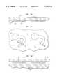
- FIG. 11is a fragmentary, bottom plan view of the components shown in FIG. 10.
- FIG. 12is a fragmentary, diagrammatic sectional view depicting the component of FIGS. 10 and 11, together with a further component during a process according to a further embodiment of the invention.
- FIGS. 13 and 14are views similar to FIG. 8, but depicting the components of FIG. 12 during progressively later stages of the process.
- FIGS. 15A through 15Eare diagrammatic, perspective, partially sectional views depicting a process according to yet another embodiment of the invention.
- FIGS. 16A through 16Hare fragmentary, diagrammatic sectional views depicting stages in a process according to yet another embodiment of the invention.
- FIGS. 17A through 17Fare views similar to FIGS. 16A-16H, but depicting a process according to a still further embodiment of the invention.
- FIG. 18is a fragmentary, perspective view depicting an assembly formed according to a process in accordance with a still further embodiment.
- FIGS. 19A and 19Bare fragmentary, diagrammatic sectional views depicting stages in a process according to yet another embodiment of the invention.
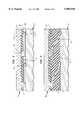
- a connection component 15 in accordance with one embodiment of the inventionincludes a structure 13 formed form a such as a dielectric sheet 10 having top and bottom surfaces and a metallic, electrically conductive reinforcing layer or sheet 26, also having top and bottom surfaces.
- Conductive layer 26overlies the top surfaces of the dielectric sheet, so that the top surface of the conductive layer defines the top surfaces of the structure, whereas the dielectric sheet defines the bottom surface of the structure.
- Conductive layer 26desirably is formed from a metal or metal alloy which is readily etchable using subtractive etching techniques.
- a copper or copper alloy sheetsuch as phosphor bronze about 100 microns to about 500 microns thick or thicker may be employed.
- Dielectric sheet 10may be formed from a polymer such as a polyimide, and typically is about 25 microns to about 75 or 100 microns thick.
- Metallic leads 12are provided on a first or bottom surface 14 of the structure.
- Each leadhas a fixed or terminal end 16 permanently attached to structure 13 by metallic elements such as via liners 17 extending into structure 13, to the metallic conductive layer 26.
- Each leadalso has a free or tip end 18 releasably attached to the bottom surface of structure 13 defined by the dielectric sheet by a small metallic button 19 projecting from the free end to the dielectric sheet and adhering to the dielectric layer over a small area.
- leads in this configurationcan be fabricated by plating an etch-resistant metal such as gold over a layer of a readily-etchable metal such as copper on the bottom surface 14 of the dielectric sheet, and then etching the resulting assembly so that the etchant removes the copper from beneath the lead.
- a readily-etchable metalsuch as copper on the bottom surface 14 of the dielectric sheet
- Each leadhas a large-diameter bulge at its fixed end, a small-diameter bulge at its free end and an elongated narrow section extending between these bulges.
- the etching processis allowed to proceed until the copper has been removed between the narrow section and the dielectric sheet, leaving copper only in the via liners 17 and buttons 19 beneath the bulges.
- the free or tip ends 18 of the leadsmay be provided with bonding materials 29 suitable for bonding the tips to contacts on the wafer.
- bonding materials 29suitable for bonding the tips to contacts on the wafer.
- the leadsare formed from gold
- eutectic bonding materialssuch as tin, germanium, silicon, tin or combinations thereof capable of forming low-melting eutectics with the gold in the leads, or alloys of these materials with gold
- Other bonding materialssuch as solders or electrically conductive polymers also can be used.
- the first elementfurther includes a rigid, ring-like frame 21 (FIG. 1) encircling structure 13.
- the frameis attached to metal layer 26 at the periphery of the layer.
- Frame 21maintains metal layer 26 and dielectric layer 10 in tension.
- the frameis arranged to maintain tension on the metal layer at all temperatures encountered during the process discussed below.
- the framemay have a coefficient of thermal expansion lower than the coefficient of thermal expansion of metal layer 10, and the frame and metal layer may be assembled, as by brazing or otherwise bonding the metal layer to the frame, while the frame and metal layer are at a temperature higher than the temperatures which will be used in the process discussed below.
- a molybdenum frame or other frame having a coefficient of thermal expansion close to that of siliconmay be used.
- the framemay be assembled to the metal sheet before or after the dielectric layer and leads are formed. Also, the frame may be attached to the dielectric layer rather than to the metal layer, provided that the frame maintains the dual-layer structure of the dielectric layer and metal layer in tension. Further techniques for using frames to maintain sheetlike structures in tension during processing are so as to achieve accurate alignment between features on the sheetlike structure and features on other elements are disclosed in the copending, commonly assigned United States Provisional Patent Application entitled “Framed Sheet Processing” filed on Oct. 17, 1997 in the names of Masud Beroz et al., the disclosure of which is incorporated by reference herein.
- structure 13, with leads 12 on its bottom surfaceis engaged with a semiconductor wafer 22 incorporating a plurality of chips 23.
- the first element including structure 13, with ring 15 thereon and the second element or wafer 22may be engaged between a pair of platens 11 and forcibly engaged with one another by urging the platens toward one another while the elements are maintained at elevated temperature. Prior to such engagement, the elements are brought into alignment with one another so that the free or tip end of each lead is in alignment with the appropriate contact 24 on the top surface 27 of the wafer.
- the elementsmay be registered with one another by registering fiducial marks (not shown) on the structure 13 or ring 15 with fiducial marks on wafer 22, using a conventional robot vision system to detect the locations of the fiducial marks.
- the fiducial marks on each elementare provided in precise registration with the other features on the same element, as by forming the fiducial marks in the same process as used to form the other features, or by forming the other features in a process using equipment registered to the fiducial marks.
- One or both elementsmay be moved in horizontal directions and rotated about a vertical axis to bring the elements into the correct registration with one another.
- wafer 22 and structure 13may be about 10-30 cm in diameter. Even over this large area, however, the tip ends of the leads may be aligned with the contacts with good precision. Several factors contribute to such precise alignment. Because structure 13 is held taut throughout the lead forming process and the aligning process by the same frame 32, the leads remain in position. Also, the free or tip ends 18 of the leads are secured to the bottom surface of structure 13 by buttons 19 at all times from the time the leads are formed up to and including the alignment process. Therefore, these ends cannot move relative to structure 13.
- frame 15has a coefficient of thermal expansion close to that of the wafer, variations in temperature during the alignment process, and during subsequent steps discussed below, will not tend to move the structure relative to the wafer. Because the frame maintains the structure in tension, thermal expansion and contraction of the structure will be substantially reflected in changes in the degree of tension in the metallic sheet, rather than in changes in size. Moreover, metallic sheet 26 controls deformation of structure 13. Because the metallic sheet is substantially stiffer than dielectric sheet 10, thermal expansion and contraction of the entire structure will be essentially the same as the thermal expansion and contraction of the metallic sheet alone. The structure has substantially uniform expansion and contraction properties over its entire area.
- the tip ends 18 of the leadsare bonded to contacts 24 on the surface of the wafer under the influence of the heat and pressure applied by platens 11.
- a gasmay be introduced under pressure between the top platen 11a (FIG. 1) and structure 13.
- the first element including structure 13 and the second element or wafer 22may be moved through a preselected displacement relative to one another with a component of motion in a vertical direction, so that the first and second elements move away from one another.
- the leads 12are bent to a vertically extensive configuration depicted in FIG. 3.
- the moving stepmay be accomplished by moving platens 11 (FIG. 1) away from one another while maintaining the elements in engagement with the platens, as by applying a vacuum through holes in the platens.
- a fluidmay be introduced under pressure between the elements so as to force the elements away from one another.
- a flowable liquid materialmay be injected between the bottom surface 14 of structure 13 defined by dielectric sheet 10 and the top surface 27 of the wafer or microelectronic element 22 concomitantly with the moving step or after the moving step, and this liquid may be cured to form a compliant layer such as an elastomer or gel layer 28 therebetween.
- the flowable liquidmay be applied under pressure to force the elements away from one another.
- etch resistant spots 30are applied on the top surface of the metallic conductive layer 26 remote from dielectric layer 10.
- the spotsare applied in registration with via liners 17.
- a photographic spot-forming processmay be registered to structure 13 using the same fiducial marks discussed above.
- Spots 30may be formed from photoresist or, as shown, from an etch resistant metal such as gold, platinum, or the like.
- the assemblyis exposed to an etchant such as an HCl and CuCl etch solution.
- Compliant layer 26 and the dielectric structure 10serve to protect microelectronic element 22 and leads 12 from the etchant during the subdividing step.
- the etchantmay be applied by immersing the assembly in the etchant or by spraying the etchant against the top surface of metallic sheet 26.
- the etchantremoves the metal of layer 26 except in the areas beneath spots 30, thereby forming subdividing the metallic sheet and forming individual terminals 32 connected to leads 12 by via liners 17.
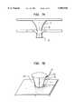
- the etchantis sprayed at a relatively high angle to the top surface, so that the etchant impinges on the top surface with a velocity vector directed almost perpendicularly to the top surface. This promotes formation of terminals 32 with the "cooling tower shape" depicted in FIG. 5.
- cooling tower shaperefers to a body having relatively large cross-sectional dimensions at a base or bottom region adjacent dielectric layer 10, tapering inwardly to narrow cross-sectional dimensions at a neck region 34 and tapering outwardly again to larger cross-sectional dimensions at a tip remote from the base.
- the cross-sectional shapes of the terminalscan be controlled by selection of the shape of spots 30.
- spots 30are circular
- terminals 32will be formed substantially as cooling tower shapes which are bodies of revolution about vertical axes 31, and hence will have circular cross-sectional shapes.
- the spotsare polygonal, such as the square spots 30' of FIG. 6B or the triangular spots 30" of FIG. 6C, the terminals 32' and 32" will have cooling tower shapes of polygonal cross-section.
- the cooling tower shapesare particularly desirable in that they can be securely received in small sockets.
- the tip 32a of a cooling tower shape terminal 32will resist disengagement from a resilient socket 35.
- the vertical edges 32a' of a cooling tower shape terminal 32' with a polygonal cross-sectionwill provide a high-force wiping contact when engaged with a round socket 35', which tends to provide a low-resistance, reliable electrical connection.
- the terminalscan be formed with shapes other than the cooling tower shapes discussed above.
- the terminals associated with the entire microelectronic elementcan be received in a single large fixture with many sockets.
- the entire wafercan be tested by engaging the assembly with a fixture so as to engage all of the terminals with sockets on the fixture simultaneously, and thereby connect all of the chips to the test fixture. After testing, the assembly can be disengaged from the fixture.
- Packaged units each including a single chip with associated portions of the dielectric structure, compliant layer and associated terminalscan be obtained by severing the wafer, dielectric structure and compliant layer along scribe lines of the wafer, i.e., along the lines of demarcation between individual chips 23.
- the terminalsare movable relative to one another and relative to the microelectronic element.
- the metallic sheetdoes not impede flexure of the flexible dielectric sheet 10.
- the flexible leadsdo not impede movement of the dielectric sheet and terminals.
- the compliant layer 28further mechanically decouples dielectric sheet 10 and terminals 32 from the microelectronic element 22. Such movability allows compensation for effects such as thermal expansion and contraction during use.
- the fixed or terminal ends of the leadsneed not be connected to the reinforcing layer 26 by straight via liners 17 as discussed above, which provide mechanical coupling.
- the dielectric layer 210 depicted in FIG. 8is composed of several sub-layers 211a-211d of dielectric material and includes several layers of internal traces 202 extending at the interfaces between the sub-layers in horizontal directions parallel to the top and bottom surfaces of the dielectric layer, and vertical conductors 204 interconnecting some of these traces.
- Layer 210can be formed by laminating several layers with prefabricated traces and through conductors to one another.
- the fixed ends 216 of leads 212are electrically connected to certain vertical conductors and traces within layer 210.
- the metallic conductive layer 226overlies the top surface of layer 210, defined by the topmost sub-layer 211a. Some of the vertical conductors and traces in turn are electrically connected to the metallic conductive layer 226, thus indirectly connecting at least some of the fixed ends to the metallic sheet.
- the fixed ends of the leadsare not mechanically connected to the conductive layer by the vertical conductors. Rather, the fixed ends of the leads are secured on the bottom surface of layer 210 by a strong metal-to-polymer bond, whereas the free ends of the leads are only weakly attached to the bottom surface of layer 210.
- terminals 232(FIG. 9) on the top surface of layer 210.
- the other process stepsmay be substantially as described above.
- some or all of the fixed ends 216may be connected through horizontally extending traces within dielectric layer 210.
- the terminals 232may be formed at locations other than directly above the fixed ends of the leads.
- the terminals 232may be more numerous or less numerous than the leads 212.
- the subdivided metallic reinforcing layermay form structures other than terminals as, for example, conductors 233 extending along the top surface of the dielectric element.
- the metallic reinforcing layercan be etched or otherwise treated to form aground plane or other potential plane.
- leads 112are formed by plating or otherwise depositing gold or another etch-resistant metal directly on the bottom surface 102 of a conductive layer 126.
- Conductive layer 126is formed from a copper-based or other etchable metal.
- Etch resistant spots 130are formed on the top surface of metal layer 126.
- Each leadhas a bonding material 113 such as a gold-tin alloy at the tip end 118 of the lead. As best seen in FIG. 10, each lead has a relatively large end portion at its fixed or terminal end 116, a somewhat smaller end portion at its free or tip end 118, and a narrow elongated portion 119 extending between these end portions. The width of elongated portion 119 is less than the diameter of either end portion.
- the bottom surface 102 of metal layer 126is exposed to an etchant for a limited time, while the top surface is protected from the etchant.
- the etchantremoves the metal of layer 126 around each lead 112, and etches progressively beneath each lead starting from the edges of the lead.
- the etching processis continued until the metal of layer 126 has been removed from beneath elongated portion 119. At this time, the etching process is stopped. At this time, the metal of layer 126 has not been entirely removed from beneath the end portions of each lead.
- the terminal end of each leadremains connected to layer 126 by a relatively large, strong metallic stem 117, whereas the tip end 118 of each lead remains connected to layer 126 by a small, weak stem 121.
- the metal layer with the leads thereonis then juxtaposed with the microelectronic element 122 and the tip ends of the leads are bonded to the contacts 124, in the same manner as discussed above (FIG. 12).
- the metal layer 126is moved upwardly, away from the microelectronic element, and a liquid material is injected between layer 126 and microelectronic element 122 to form a compliant layer 128.
- the metal layeracts as the first element in the process of deforming the leads as discussed above, whereas the microelectronic element acts as the second element.
- the metal layer 126is etched from its top surface in the same manner as described above, to form terminals 132 beneath the etch-resistant spots 130. Each such terminal remains connected to the fixed or terminal end 116 of a lead 112 by the stem 117 formed earlier in the process.
- the resulting assemblycan be used in substantially the same manner as the assemblies described above.
- the individual terminalsare movable relative to one another and relative to the microelectronic element.
- the processcan be used with individual semiconductor chips or other individual microelectronic devices, rather than with a wafer as discussed above. In this case, there is no need to sever the dielectric layer.
- the order of stepsmay be varied. Thus, the step of removing portions of the conductive layer so as to subdivide the conductive layer and form terminals may be performed before the step of moving the elements and deforming the leads.
- the conductive layermay be formed from electrically conductive materials other than metals, such as conductive polymer compositions. Portions of the conductive layer may be removed by processes other than etching as, for example, laser ablation or mechanical processes.
- the material used to form reinforcing layer 26 and hence used to form terminals 32can be selected to have a coefficient of thermal expansion close to that of the microelectronic element.
- the tip ends of the leads or the contacts on the chipscan be provided with a bonding alloy or conductive adhesive that can be activated at a low temperature.
- the techniques discussed abovecan be used to form assemblies according to the teachings of copending, commonly assigned U.S. patent application Ser. Nos. 08/532,528 filed Sep. 22, 1995 and 08/678,808 Filed Jul. 12, 1996 the disclosures of which are also incorporated by reference herein.
- the restraining strapstypically are stronger than the leads and shorter than the leads.
- the restraining strapslimit and constrain the relative motion of the elements so that the leads are not pulled taut.
- the restraining strapscan be mechanically connected to the conductive layer.
- the conductive layerdesirably reinforces the structure and maintains it planar. Therefore, if a fluid is introduced to force the elements away from one another, the structure will remain planar even if no external constraining element is applied.
- a fluid under pressuremay be provided between the elements by use of a foamable material, as taught in commonly assigned United States Provisional Patent Application 60/032,870 filed Dec. 13, 1996, the disclosure of which is also incorporated by reference herein.
- the frame discussed abovecan be varied.
- the frameneed not be circular, but instead can be rectangular or have any other shape.
- the frameneed not form a closed loop entirely encircling the structure formed by the dielectric sheet and the conductive reinforcing layer.
- the framemay have two or more discrete elements attached to the structure at spaced apart locations so that the frame holds the structure in tension.
- the framecan be formed in various ways, as by etching a solid sheet of a rigid material or machining the sheet to form an opening. In a process according to a further alternative, the frame is omitted entirely.
- the electrically conductive layer aloneis sufficient to maintain dimensional stability of the structure and to maintain known, controllable spacings between the tip ends of the leads.
- a frame 315is formed integrally with a metallic reinforcing sheet or layer 326 (FIG. 15A).
- frame 315 and the structure including metallic layer 326define a cup-shaped recess 340 which is open at a first end and which is closed at the other end by the structure or layer 326.
- Leads 312are provided on the surface 330 of the structure or layer 326 which faces into the recess at the closed end.
- a dielectric layer(not shown) similar to the dielectric layer 10 of FIGS. 2-3 may also be provided at surface 330.
- the combinationfurther includes a port 342 extending into recess 340 at or adjacent to the closed end or surface 330. As illustrated, port 342 extends through layer or structure 326 outside of the area occupied by leads 312. However, the port can also extend through frame 315.
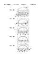
- a wafer or other microelectronic element 322is placed into recess 340 and contacts on a surface of the wafer are bonded to the free ends of leads 312 in the manner discussed above (FIG. 15B).
- a flexible sealsuch as a tape, diaphragm or gasket (not shown) is provided between the microelectronic element or wafer 322 and frame 315.
- a fluid under pressurepreferably a curable liquid is introduced through port 342 so as to force the microelectronic element 322 and the structure including conductive layer 326 away from one another, thereby deforming leads 312 to a more vertically extensive disposition in the manner discussed above, and forcing the microelectronic element toward the open end of the recess.
- the degree of relative movementmay be limited by external applied elements such as a plate resting on the surface 344 of frame 315, or by engaging frame 315 between a pair of flat plates.
- the degree of relative movementmay be controlled by restraining straps as discussed above interspersed with leads 312 and connected between structure 326 and the microelectronic element.
- the curable material 328is then cured to form a compliant layer (FIG. 15D).
- the conductive layer 326is partially removed, as by etching to subdivide the layer and form terminals 332.
- Other featuressuch as leads or potential planes can be formed in lieu of or in addition to the terminals.
- the etching step used to subdivide sheet 326may also remove part of frame 315.
- the assembly including the wafer or microelectronic element 322 and the terminals 332 connected thereto by flexible leads 312can be stored and shipped.
- Part of frame 315remains in place and helps to protect the relatively delicate wafer from physical damage.
- the framemay be removed by sawing it away from neighboring portions of the wafer in the same process used to subdivide the wafer and the dielectric element to form individual chip packages.
- the framemay be removed prior to processing, as by separately machining or etching the frame away.
- the assembly of the wafer 322, dielectric element terminals and leadscan be pushed out of the frame. To allow removal in this manner, the dielectric material should not adhere strongly to the surfaces of the frame forming the walls of recess 340.
- the wall surfacesmay be coated with a release agent such as a fluropolymer.
- the frameserves as a disposable fixture for use in the process of injecting the curable liquid. This avoids the problems associated with cleaning and reusing fixtures.
- the same processcan be employed where the conductive layer and the frame are not formed integrally with one another, but are attached to one another.
- a structure 413is formed by applying a temporary layer 410 on the bottom surface of a metallic conductive layer 426 (FIGS. 16A-16B).
- Layer 410may be formed from a material which can be etched or dissolved and which has only limited adhesion to the surface of layer 426. Polymeric materials such as polyimide can be employed. Other polymers which can survive at the temperatures used in the bonding operation used to connect the leads to the microelectronic element may also be employed.
- Apertures 440are formed in layer 410. These apertures may be formed by selectively applying the temporary layer, by laser ablating the temporary layer or by selectively etching the temporary layer.
- Metallic leads 412(FIG.
- each lead 16Dare then deposited on the surface of temporary layer 410, so that a fixed or terminal end 416 of each lead is connected to sheet 426 by a stem 417 integral with the lead and extending through one of the apertures 440 in layer 410.
- Leads 412have a configuration similar to that discussed above with reference to FIGS. 10 and 11. Thus, each lead includes a narrow elongated section 419 extending from the fixed or terminal end 416 to the free or tip end 418 of the lead and a relatively wide, bulging section at the free or tip end.
- the structureis exposed to a solvent or etchant which attacks the material of temporary layer 410 but which does not substantially attack the material of leads 412 or conductive layer 426.
- a solvent or etchantwhich attacks the material of temporary layer 410 but which does not substantially attack the material of leads 412 or conductive layer 426.
- the structuremay be exposed to a plasma which attacks the polyimide.
- layer 410is composed from a soluble polymer
- the structuremay be exposed to a liquid solvent which dissolves away the polymer.
- the relatively broad tip ends of the leadsprotect the underlying material of temporary layer 410, so that small buttons of the polymer or other material in the temporary layer remain when the portions of layer 410 beneath the elongated sections 419 of the leads are entirely removed.
- the temporary layer 410may also remain beneath the lead at the terminal or fixed end 416. Buttons 421 releasably hold the tip or free ends 418 of the leads to conductive layer 426.
- the tip endsare bonded to contacts on the wafer or microelectronic element 422 using bonding material 424 which may be carried either on the free ends of the leads or on the contacts of the microelectronic element.
- buttons 421provide limited adhesion between the tip ends of the leads and the conductive layer and thus permit easy release of the leads from the conductive layer during the process. However, the buttons 421 provide adequate adhesion to hold the free ends of the leads in position prior to bonding with the microelectronic element.
- FIGS. 17A-17Fis identical to the process of FIGS. 16A-16H except that in the process of FIGS. 17A-17F, cavities 501 are formed in a sheet which forms part of the conductive layer 526.
- the cavitiesare provided in alignment with the openings 540 of the temporary layer 510 before application of metal to form leads 512.
- Cavities 501may be formed by etching the sheet before application of layer 510 or by etching the sheet after application of the temporary layer, using layer 510 as a mask.
- the lead-forming metalis applied, is substantially fills cavities 501 and forms generally dome-shaped bumps or masses 550 extending within conductive layer 526 and forming parts of the conductive layer.
- the lead-forming metalhas a greater resistance to etching than the metal constituting the remainder of layer 526.
- the leads and hence masses 550may be formed from gold.
- the conductive layer in this embodimentincludes masses of a first metal such as gold spaced apart from one another within a sheet of a second metal such as copper.
- etching or dissolving the temporary layer to form buttons 521, bonding the free ends 518 of the leads to the microelectronic element and moving the structure including conductive layer 526 away from the microelectronic element 522proceeds in the same manner as discussed above.
- conductive layer 526is exposed to an etchant without preliminary masking or depositing spots on the top surface of the layer.
- the etchantremoves all of the second material in layer 526 other than the material of masses 550, leaving the masses as isolated terminals.
- the material of the massesacts as etch resistant portions of the conductive layer.
- Differential etchingis achieved by differing etch resistances in the material of the layer, rather than by masking the layer.
- Similar techniquesproviding especially etch resistant material in masses of the conductive layer, can be used to form other elements as, for example, leads extending along the surface of the dielectric layer 528.
- the same techniquescan be combined with use of a permanent dielectric layer underlying the conductive layer, similar to layer 10 discussed above with reference to FIGS. 1-5, or with a multilayer dielectric layer as discussed above with reference to FIGS. 8 and 9.
- the especially etch resistant materialcan be provided in configuration other than the dome-shaped masses, and need not be formed from the same material as the lead.
- the second or less etch-resistant material included in conductive layer 526need not be conductive.
- the step of etching or otherwise partially removing the conductive layermay be performed so as to provide portions of the conductive layer having different thicknesses.
- the conductive layermay be removed by etching most of the surface deeply, so as to leave only a thin, flexible potential plane layer 630.
- Other portions of the surfaceare protected by etch resistant materials 640 and hence are not etched and remain as terminals 632. These terminals have a height substantially equal to the thickness of the original layer.
- Still other portionsare etched entirely through the conductive layer, so as to form openings 636 in layer 630 surrounding each terminal 632 and thereby electrically isolating the terminals from the potential plane layer.
- a photoimageable masking materialmay be applied on the surface of layer 630 and exposed to form apertures in the masking material corresponding to apertures 636. The etching process is then continued until the apertures 636 extend over layer 630.
- the conductive layeris etched to a reduced thickness of its entire surface and left as a continuous but flexible sheet. Stated another way, the conductive layer is not subdivided. Rather, portions of the material constituting the conductive layer are removed so that the remaining layer does not impair flexibility of the adjacent flexible or compliant layers.
- the stiff, reinforcing conductive layeris converted to a flexible conductive element of the finished device or to a plurality of individual, mutually movable conductive elements such as the individual terminals discussed above.
- the conductive layer 726is connected to the microelectronic element 722 by conductive attachment elements 712 which are not flexible and which are not deformed by relative movement of the structures in the manner discussed above. Rather, conductive attachment elements 712 may be substantially rigid posts applied to the conductive layer or formed by partial etching of conductive layer 726 at a bottom surface 727. The attachment elements may be provided with bonding materials at their tips 713 remote from layer 726. The structure including layer 726 and attachment elements 712 is juxtaposed with the wafer or other microelectronic element 722 as shown in FIG. 19A.
- the rigidity of the conductive layer 726contributes to the dimensional stability of the structure and allows accurate alignment of the attachment elements 712 with contacts 724 on the wafer or other microelectronic element.
- the structure including conductive layer 726is spaced apart from the top surface of microelectronic element 722 by the attachment elements.
- a dielectric materialsuch as a compliant material 728 is introduced between the structure 726 and the surface of the microelectronic element 722.
- the conductive layeris again etched to form terminals 732 connected to conductive elements 712 and hence connected to wafer 722.
- etching or partial removal of the conductive sheetessentially eliminates rigidity of the sheet, leaving each terminal 732 and the associated conductive element 712 and chip contact 724 independent of the others.
- the wafercan be severed to provide individual units, each including a portion of the wafer and the associated terminals.
- a flexible dielectric layersimilar to layer 10 discussed above is provided on the bottom surface 727 of the conductive layer and remains as a part of the finished assembly, overlying dielectric layer 728.
- processes according to this embodiment of the inventionare more preferably utilize when individual connections will not be subjected to high thermal cycling strains as, for example, when the chips to be cut from the wafer are small and when the chips will be used with substrates which are well-matched to the chips in thermal expansion properties.
Landscapes
- Engineering & Computer Science (AREA)
- Microelectronics & Electronic Packaging (AREA)
- Computer Hardware Design (AREA)
- Power Engineering (AREA)
- Physics & Mathematics (AREA)
- Condensed Matter Physics & Semiconductors (AREA)
- General Physics & Mathematics (AREA)
- Manufacturing & Machinery (AREA)
- Wire Bonding (AREA)
Abstract
Description
Claims (28)
Priority Applications (6)
| Application Number | Priority Date | Filing Date | Title |
|---|---|---|---|
| US08/989,312US5989936A (en) | 1994-07-07 | 1997-12-12 | Microelectronic assembly fabrication with terminal formation from a conductive layer |
| US09/267,058US6117694A (en) | 1994-07-07 | 1999-03-12 | Flexible lead structures and methods of making same |
| US09/395,105US6307260B1 (en) | 1994-07-07 | 1999-09-14 | Microelectronic assembly fabrication with terminal formation from a conductive layer |
| US09/405,029US6499216B1 (en) | 1994-07-07 | 1999-09-24 | Methods and structures for electronic probing arrays |
| US10/290,010US6828668B2 (en) | 1994-07-07 | 2002-11-07 | Flexible lead structures and methods of making same |
| US10/728,308US6876212B2 (en) | 1994-07-07 | 2003-12-04 | Methods and structures for electronic probing arrays |
Applications Claiming Priority (6)
| Application Number | Priority Date | Filing Date | Title |
|---|---|---|---|
| US08/271,768US5518964A (en) | 1994-07-07 | 1994-07-07 | Microelectronic mounting with multiple lead deformation and bonding |
| US36623694A | 1994-12-29 | 1994-12-29 | |
| US08/440,665US5801441A (en) | 1994-07-07 | 1995-05-15 | Microelectronic mounting with multiple lead deformation and bonding |
| US3282896P | 1996-12-13 | 1996-12-13 | |
| US08/885,238US6177636B1 (en) | 1994-12-29 | 1997-06-30 | Connection components with posts |
| US08/989,312US5989936A (en) | 1994-07-07 | 1997-12-12 | Microelectronic assembly fabrication with terminal formation from a conductive layer |
Related Parent Applications (2)
| Application Number | Title | Priority Date | Filing Date |
|---|---|---|---|
| US08/440,665Continuation-In-PartUS5801441A (en) | 1994-07-07 | 1995-05-15 | Microelectronic mounting with multiple lead deformation and bonding |
| US08/885,238Continuation-In-PartUS6177636B1 (en) | 1994-07-07 | 1997-06-30 | Connection components with posts |
Related Child Applications (3)
| Application Number | Title | Priority Date | Filing Date |
|---|---|---|---|
| US09/267,058Continuation-In-PartUS6117694A (en) | 1994-07-07 | 1999-03-12 | Flexible lead structures and methods of making same |
| US09/395,105DivisionUS6307260B1 (en) | 1994-07-07 | 1999-09-14 | Microelectronic assembly fabrication with terminal formation from a conductive layer |
| US65930200AContinuation | 1994-07-07 | 2000-09-12 |
Publications (1)
| Publication Number | Publication Date |
|---|---|
| US5989936Atrue US5989936A (en) | 1999-11-23 |
Family
ID=27534426
Family Applications (2)
| Application Number | Title | Priority Date | Filing Date |
|---|---|---|---|
| US08/989,312Expired - LifetimeUS5989936A (en) | 1994-07-07 | 1997-12-12 | Microelectronic assembly fabrication with terminal formation from a conductive layer |
| US09/395,105Expired - LifetimeUS6307260B1 (en) | 1994-07-07 | 1999-09-14 | Microelectronic assembly fabrication with terminal formation from a conductive layer |
Family Applications After (1)
| Application Number | Title | Priority Date | Filing Date |
|---|---|---|---|
| US09/395,105Expired - LifetimeUS6307260B1 (en) | 1994-07-07 | 1999-09-14 | Microelectronic assembly fabrication with terminal formation from a conductive layer |
Country Status (1)
| Country | Link |
|---|---|
| US (2) | US5989936A (en) |
Cited By (94)
| Publication number | Priority date | Publication date | Assignee | Title |
|---|---|---|---|---|
| US6063648A (en)* | 1998-10-29 | 2000-05-16 | Tessera, Inc. | Lead formation usings grids |
| US6083772A (en)* | 1997-01-02 | 2000-07-04 | Lucent Technologies Inc. | Method of mounting a power semiconductor die on a substrate |
| US6117694A (en)* | 1994-07-07 | 2000-09-12 | Tessera, Inc. | Flexible lead structures and methods of making same |
| WO2000064229A1 (en)* | 1999-04-15 | 2000-10-26 | Amerasia International Technology, Inc. | Contact module, as for a smart card, and method for making same |
| US6207548B1 (en)* | 1996-03-07 | 2001-03-27 | Micron Technology, Inc. | Method for fabricating a micromachined chip scale package |
| US6228686B1 (en) | 1995-09-18 | 2001-05-08 | Tessera, Inc. | Method of fabricating a microelectronic assembly using sheets with gaps to define lead regions |
| US20010028102A1 (en)* | 2000-04-10 | 2001-10-11 | Hans-Jurgen Hacke | Electronic component having microscopically small contact areas and method for fabricating it |
| US6361959B1 (en) | 1994-07-07 | 2002-03-26 | Tessera, Inc. | Microelectronic unit forming methods and materials |
| DE10110005A1 (en)* | 2001-03-01 | 2002-09-19 | Infineon Technologies Ag | Electronic component used as semiconductor comprises semiconductor chip having active front side with bond pads and covered with elastic layer provided with contacts electrically conductively connected to bond pads |
| US6461892B2 (en) | 2000-01-26 | 2002-10-08 | Tessera, Inc. | Methods of making a connection component using a removable layer |
| US6468830B1 (en)* | 1998-01-26 | 2002-10-22 | Tessera, Inc. | Compliant semiconductor package with anisotropic conductive material interconnects and methods therefor |
| US6495462B1 (en)* | 1998-02-09 | 2002-12-17 | Tessera, Inc. | Components with releasable leads |
| US6499216B1 (en) | 1994-07-07 | 2002-12-31 | Tessera, Inc. | Methods and structures for electronic probing arrays |
| US20030068906A1 (en)* | 2001-05-09 | 2003-04-10 | David Light | Connection components with anisotropic conductive material interconnection |
| US20030071346A1 (en)* | 1994-07-07 | 2003-04-17 | Tessera, Inc. | Flexible lead structures and methods of making same |
| US20030075358A1 (en)* | 2001-09-13 | 2003-04-24 | Tessera, Inc. | Microelectronic assembly formation with releasable leads |
| US6555849B1 (en) | 1998-05-12 | 2003-04-29 | Infineon Technologies Ag | Deactivatable thyristor |
| US20030101584A1 (en)* | 1998-06-09 | 2003-06-05 | Shigeru Matsumura | Bump and method of forming bump |
| US20030139029A1 (en)* | 1999-03-10 | 2003-07-24 | Belgacem Haba | Joining semiconductor units with bonding material |
| US6620647B2 (en)* | 2000-02-03 | 2003-09-16 | Infineon Technologies Ag | Method for producing a semiconductor component with a silicon carrier substrate |
| US6657286B2 (en) | 2000-09-21 | 2003-12-02 | Tessera, Inc. | Microelectronic assembly formation with lead displacement |
| US6661247B2 (en) | 1997-09-19 | 2003-12-09 | Fujitsu Limited | Semiconductor testing device |
| US6664621B2 (en) | 2000-05-08 | 2003-12-16 | Tessera, Inc. | Semiconductor chip package with interconnect structure |
| US6690186B2 (en) | 1994-07-07 | 2004-02-10 | Tessera, Inc. | Methods and structures for electronic probing arrays |
| US6709906B2 (en) | 1994-02-28 | 2004-03-23 | Semiconductor Energy Laboratory Co., Ltd. | Method for producing semiconductor device |
| US6713374B2 (en)* | 1999-07-30 | 2004-03-30 | Formfactor, Inc. | Interconnect assemblies and methods |
| US6808958B2 (en) | 2001-03-07 | 2004-10-26 | Tessera, Inc. | Methods of bonding microelectronic elements |
| US20050023680A1 (en)* | 2003-07-31 | 2005-02-03 | Wang James Jen-Ho | Semiconductor device with strain relieving bump design |
| US20050048696A1 (en)* | 1999-08-26 | 2005-03-03 | Honeywell, Inc. | Microbeam assembly and associated method for integrated circuit interconnection to substrates |
| US20050189640A1 (en)* | 2003-11-13 | 2005-09-01 | Grundy Kevin P. | Interconnect system without through-holes |
| US20060113680A1 (en)* | 1997-09-18 | 2006-06-01 | Tessera, Inc. | Microelectronic packages with solder interconnections |
| US20060194365A1 (en)* | 2005-02-25 | 2006-08-31 | Tessera, Inc. | Microelectronic assemblies having compliancy |
| US20060244468A1 (en)* | 2005-04-29 | 2006-11-02 | Wen-Chang Dong | Micro-electromechanical probe circuit substrate |
| US20070158816A1 (en)* | 2006-01-12 | 2007-07-12 | Palo Alto Research Center Incorporated | Contact spring application to semiconductor devices |
| US20070289729A1 (en)* | 2006-06-16 | 2007-12-20 | International Business Machines Corporation | Thermally conductive composite interface, cooled electronic assemblies employing the same, and methods of fabrication thereof |
| US20080150121A1 (en)* | 2006-12-20 | 2008-06-26 | Tessera Technologies Hungary Kft. | Microelectronic assemblies having compliancy and methods therefor |
| US7435108B1 (en) | 1999-07-30 | 2008-10-14 | Formfactor, Inc. | Variable width resilient conductive contact structures |
| US20090104736A1 (en)* | 2004-11-03 | 2009-04-23 | Tessera, Inc. | Stacked Packaging Improvements |
| US7723831B2 (en) | 2007-05-17 | 2010-05-25 | Micron Technology, Inc. | Semiconductor package having die with recess and discrete component embedded within the recess |
| US20100171227A1 (en)* | 2007-06-07 | 2010-07-08 | Commissariat A L'energie Atomique | Method of producing a via in a reconstituted substrate |
| US20100203721A1 (en)* | 2002-08-29 | 2010-08-12 | Hiatt William M | Multi-component integrated circuit contacts |
| US20110056243A1 (en)* | 2009-09-09 | 2011-03-10 | Stars Of Africa Corp. | Novel jewelry piece or article and method of making |
| US20110165733A1 (en)* | 2005-12-23 | 2011-07-07 | Tessera, Inc. | Microelectronic packages and methods therefor |
| US8021976B2 (en) | 2002-10-15 | 2011-09-20 | Megica Corporation | Method of wire bonding over active area of a semiconductor circuit |
| US20110247872A1 (en)* | 2010-04-08 | 2011-10-13 | Qing Ma | Debond interconnect structures |
| US8148806B2 (en) | 2000-05-19 | 2012-04-03 | Megica Corporation | Multiple chips bonded to packaging structure with low noise and multiple selectable functions |
| US8168527B2 (en) | 2006-09-06 | 2012-05-01 | Megica Corporation | Semiconductor chip and method for fabricating the same |
| US8404520B1 (en)* | 2011-10-17 | 2013-03-26 | Invensas Corporation | Package-on-package assembly with wire bond vias |
| US8426982B2 (en) | 2001-03-30 | 2013-04-23 | Megica Corporation | Structure and manufacturing method of chip scale package |
| US8482111B2 (en) | 2010-07-19 | 2013-07-09 | Tessera, Inc. | Stackable molded microelectronic packages |
| US8618659B2 (en) | 2011-05-03 | 2013-12-31 | Tessera, Inc. | Package-on-package assembly with wire bonds to encapsulation surface |
| US8623706B2 (en) | 2010-11-15 | 2014-01-07 | Tessera, Inc. | Microelectronic package with terminals on dielectric mass |
| US8835228B2 (en) | 2012-05-22 | 2014-09-16 | Invensas Corporation | Substrate-less stackable package with wire-bond interconnect |
| US8878353B2 (en) | 2012-12-20 | 2014-11-04 | Invensas Corporation | Structure for microelectronic packaging with bond elements to encapsulation surface |
| US8883563B1 (en) | 2013-07-15 | 2014-11-11 | Invensas Corporation | Fabrication of microelectronic assemblies having stack terminals coupled by connectors extending through encapsulation |
| US8975738B2 (en) | 2012-11-12 | 2015-03-10 | Invensas Corporation | Structure for microelectronic packaging with terminals on dielectric mass |
| US9023691B2 (en) | 2013-07-15 | 2015-05-05 | Invensas Corporation | Microelectronic assemblies with stack terminals coupled by connectors extending through encapsulation |
| US9034696B2 (en) | 2013-07-15 | 2015-05-19 | Invensas Corporation | Microelectronic assemblies having reinforcing collars on connectors extending through encapsulation |
| US9082753B2 (en) | 2013-11-12 | 2015-07-14 | Invensas Corporation | Severing bond wire by kinking and twisting |
| US9087815B2 (en) | 2013-11-12 | 2015-07-21 | Invensas Corporation | Off substrate kinking of bond wire |
| US20150262957A1 (en)* | 2014-03-11 | 2015-09-17 | Shinko Electric Industries Co., Ltd. | Semiconductor package |
| US9214454B2 (en) | 2014-03-31 | 2015-12-15 | Invensas Corporation | Batch process fabrication of package-on-package microelectronic assemblies |
| US9224717B2 (en) | 2011-05-03 | 2015-12-29 | Tessera, Inc. | Package-on-package assembly with wire bonds to encapsulation surface |
| US9324681B2 (en) | 2010-12-13 | 2016-04-26 | Tessera, Inc. | Pin attachment |
| US9349706B2 (en) | 2012-02-24 | 2016-05-24 | Invensas Corporation | Method for package-on-package assembly with wire bonds to encapsulation surface |
| US9391008B2 (en) | 2012-07-31 | 2016-07-12 | Invensas Corporation | Reconstituted wafer-level package DRAM |
| US9412714B2 (en) | 2014-05-30 | 2016-08-09 | Invensas Corporation | Wire bond support structure and microelectronic package including wire bonds therefrom |
| US9502390B2 (en) | 2012-08-03 | 2016-11-22 | Invensas Corporation | BVA interposer |
| US9553076B2 (en) | 2010-07-19 | 2017-01-24 | Tessera, Inc. | Stackable molded microelectronic packages with area array unit connectors |
| US9583411B2 (en) | 2014-01-17 | 2017-02-28 | Invensas Corporation | Fine pitch BVA using reconstituted wafer with area array accessible for testing |
| US9601454B2 (en) | 2013-02-01 | 2017-03-21 | Invensas Corporation | Method of forming a component having wire bonds and a stiffening layer |
| US9646917B2 (en) | 2014-05-29 | 2017-05-09 | Invensas Corporation | Low CTE component with wire bond interconnects |
| US9659848B1 (en) | 2015-11-18 | 2017-05-23 | Invensas Corporation | Stiffened wires for offset BVA |
| US9685365B2 (en) | 2013-08-08 | 2017-06-20 | Invensas Corporation | Method of forming a wire bond having a free end |
| US9691679B2 (en) | 2012-02-24 | 2017-06-27 | Invensas Corporation | Method for package-on-package assembly with wire bonds to encapsulation surface |
| US9728527B2 (en) | 2013-11-22 | 2017-08-08 | Invensas Corporation | Multiple bond via arrays of different wire heights on a same substrate |
| US9735084B2 (en) | 2014-12-11 | 2017-08-15 | Invensas Corporation | Bond via array for thermal conductivity |
| US9761554B2 (en) | 2015-05-07 | 2017-09-12 | Invensas Corporation | Ball bonding metal wire bond wires to metal pads |
| US9812402B2 (en) | 2015-10-12 | 2017-11-07 | Invensas Corporation | Wire bond wires for interference shielding |
| US9842745B2 (en) | 2012-02-17 | 2017-12-12 | Invensas Corporation | Heat spreading substrate with embedded interconnects |
| US9852969B2 (en) | 2013-11-22 | 2017-12-26 | Invensas Corporation | Die stacks with one or more bond via arrays of wire bond wires and with one or more arrays of bump interconnects |
| US9888579B2 (en) | 2015-03-05 | 2018-02-06 | Invensas Corporation | Pressing of wire bond wire tips to provide bent-over tips |
| US9911718B2 (en) | 2015-11-17 | 2018-03-06 | Invensas Corporation | ‘RDL-First’ packaged microelectronic device for a package-on-package device |
| US9935075B2 (en) | 2016-07-29 | 2018-04-03 | Invensas Corporation | Wire bonding method and apparatus for electromagnetic interference shielding |
| US9984992B2 (en) | 2015-12-30 | 2018-05-29 | Invensas Corporation | Embedded wire bond wires for vertical integration with separate surface mount and wire bond mounting surfaces |
| US10008477B2 (en) | 2013-09-16 | 2018-06-26 | Invensas Corporation | Microelectronic element with bond elements to encapsulation surface |
| US10008469B2 (en) | 2015-04-30 | 2018-06-26 | Invensas Corporation | Wafer-level packaging using wire bond wires in place of a redistribution layer |
| US10026717B2 (en) | 2013-11-22 | 2018-07-17 | Invensas Corporation | Multiple bond via arrays of different wire heights on a same substrate |
| US10181457B2 (en) | 2015-10-26 | 2019-01-15 | Invensas Corporation | Microelectronic package for wafer-level chip scale packaging with fan-out |
| US10299368B2 (en) | 2016-12-21 | 2019-05-21 | Invensas Corporation | Surface integrated waveguides and circuit structures therefor |
| US10332854B2 (en) | 2015-10-23 | 2019-06-25 | Invensas Corporation | Anchoring structure of fine pitch bva |
| US10381326B2 (en) | 2014-05-28 | 2019-08-13 | Invensas Corporation | Structure and method for integrated circuits packaging with increased density |
| US10460958B2 (en) | 2013-08-07 | 2019-10-29 | Invensas Corporation | Method of manufacturing embedded packaging with preformed vias |
| US10490528B2 (en) | 2015-10-12 | 2019-11-26 | Invensas Corporation | Embedded wire bond wires |
Families Citing this family (20)
| Publication number | Priority date | Publication date | Assignee | Title |
|---|---|---|---|---|
| US6261863B1 (en)* | 1995-10-24 | 2001-07-17 | Tessera, Inc. | Components with releasable leads and methods of making releasable leads |
| JP3180800B2 (en)* | 1999-04-08 | 2001-06-25 | カシオ計算機株式会社 | Semiconductor device and manufacturing method thereof |
| US7265045B2 (en) | 2002-10-24 | 2007-09-04 | Megica Corporation | Method for fabricating thermal compliant semiconductor chip wiring structure for chip scale packaging |
| US7495179B2 (en) | 2003-10-06 | 2009-02-24 | Tessera, Inc. | Components with posts and pads |
| US7462936B2 (en)* | 2003-10-06 | 2008-12-09 | Tessera, Inc. | Formation of circuitry with modification of feature height |
| US8641913B2 (en)* | 2003-10-06 | 2014-02-04 | Tessera, Inc. | Fine pitch microcontacts and method for forming thereof |
| US8207604B2 (en)* | 2003-12-30 | 2012-06-26 | Tessera, Inc. | Microelectronic package comprising offset conductive posts on compliant layer |
| US7709968B2 (en)* | 2003-12-30 | 2010-05-04 | Tessera, Inc. | Micro pin grid array with pin motion isolation |
| US7750487B2 (en)* | 2004-08-11 | 2010-07-06 | Intel Corporation | Metal-metal bonding of compliant interconnect |
| ITMI20060478A1 (en)* | 2006-03-16 | 2007-09-17 | Eles Semiconductor Equipment Spa | SYSTEM FOR CONTACTING ELECTRONIC DEVICES AND ITS PRODUCTION METHOD BASED ON WIRED CONDUCTOR IN INSULATING MATERIAL |
| JP5629580B2 (en) | 2007-09-28 | 2014-11-19 | テッセラ,インコーポレイテッド | Flip chip interconnect with double posts |
| US20100044860A1 (en)* | 2008-08-21 | 2010-02-25 | Tessera Interconnect Materials, Inc. | Microelectronic substrate or element having conductive pads and metal posts joined thereto using bond layer |
| US8278748B2 (en) | 2010-02-17 | 2012-10-02 | Maxim Integrated Products, Inc. | Wafer-level packaged device having self-assembled resilient leads |
| US8330272B2 (en) | 2010-07-08 | 2012-12-11 | Tessera, Inc. | Microelectronic packages with dual or multiple-etched flip-chip connectors |
| US8580607B2 (en) | 2010-07-27 | 2013-11-12 | Tessera, Inc. | Microelectronic packages with nanoparticle joining |
| US8853558B2 (en) | 2010-12-10 | 2014-10-07 | Tessera, Inc. | Interconnect structure |
| US10886250B2 (en) | 2015-07-10 | 2021-01-05 | Invensas Corporation | Structures and methods for low temperature bonding using nanoparticles |
| US9633971B2 (en) | 2015-07-10 | 2017-04-25 | Invensas Corporation | Structures and methods for low temperature bonding using nanoparticles |
| TWI822659B (en) | 2016-10-27 | 2023-11-21 | 美商艾德亞半導體科技有限責任公司 | Structures and methods for low temperature bonding |
| JP2024501559A (en) | 2020-12-30 | 2024-01-12 | アデイア セミコンダクター ボンディング テクノロジーズ インコーポレイテッド | Structures with conductive features and methods of forming the same |
Citations (19)
| Publication number | Priority date | Publication date | Assignee | Title |
|---|---|---|---|---|
| US4067104A (en)* | 1977-02-24 | 1978-01-10 | Rockwell International Corporation | Method of fabricating an array of flexible metallic interconnects for coupling microelectronics components |
| US4642889A (en)* | 1985-04-29 | 1987-02-17 | Amp Incorporated | Compliant interconnection and method therefor |
| US4955523A (en)* | 1986-12-17 | 1990-09-11 | Raychem Corporation | Interconnection of electronic components |
| US5067007A (en)* | 1988-06-13 | 1991-11-19 | Hitachi, Ltd. | Semiconductor device having leads for mounting to a surface of a printed circuit board |
| US5133495A (en)* | 1991-08-12 | 1992-07-28 | International Business Machines Corporation | Method of bonding flexible circuit to circuitized substrate to provide electrical connection therebetween |
| US5148265A (en)* | 1990-09-24 | 1992-09-15 | Ist Associates, Inc. | Semiconductor chip assemblies with fan-in leads |
| US5148266A (en)* | 1990-09-24 | 1992-09-15 | Ist Associates, Inc. | Semiconductor chip assemblies having interposer and flexible lead |
| US5203075A (en)* | 1991-08-12 | 1993-04-20 | Inernational Business Machines | Method of bonding flexible circuit to cicuitized substrate to provide electrical connection therebetween using different solders |
| US5258330A (en)* | 1990-09-24 | 1993-11-02 | Tessera, Inc. | Semiconductor chip assemblies with fan-in leads |
| US5316788A (en)* | 1991-07-26 | 1994-05-31 | International Business Machines Corporation | Applying solder to high density substrates |
| US5398863A (en)* | 1993-07-23 | 1995-03-21 | Tessera, Inc. | Shaped lead structure and method |
| US5455390A (en)* | 1994-02-01 | 1995-10-03 | Tessera, Inc. | Microelectronics unit mounting with multiple lead bonding |
| US5518964A (en)* | 1994-07-07 | 1996-05-21 | Tessera, Inc. | Microelectronic mounting with multiple lead deformation and bonding |
| US5525545A (en)* | 1993-03-26 | 1996-06-11 | Tessera, Inc. | Semiconductor chip assemblies and components with pressure contact |
| US5557501A (en)* | 1994-11-18 | 1996-09-17 | Tessera, Inc. | Compliant thermal connectors and assemblies incorporating the same |
| US5590460A (en)* | 1994-07-19 | 1997-01-07 | Tessera, Inc. | Method of making multilayer circuit |
| US5615824A (en)* | 1994-06-07 | 1997-04-01 | Tessera, Inc. | Soldering with resilient contacts |
| US5679977A (en)* | 1990-09-24 | 1997-10-21 | Tessera, Inc. | Semiconductor chip assemblies, methods of making same and components for same |
| US5688716A (en)* | 1994-07-07 | 1997-11-18 | Tessera, Inc. | Fan-out semiconductor chip assembly |
Family Cites Families (1)
| Publication number | Priority date | Publication date | Assignee | Title |
|---|---|---|---|---|
| US5210939A (en)* | 1992-04-17 | 1993-05-18 | Intel Corporation | Lead grid array integrated circuit |
- 1997
- 1997-12-12USUS08/989,312patent/US5989936A/ennot_activeExpired - Lifetime
- 1999
- 1999-09-14USUS09/395,105patent/US6307260B1/ennot_activeExpired - Lifetime
Patent Citations (21)
| Publication number | Priority date | Publication date | Assignee | Title |
|---|---|---|---|---|
| US4067104A (en)* | 1977-02-24 | 1978-01-10 | Rockwell International Corporation | Method of fabricating an array of flexible metallic interconnects for coupling microelectronics components |
| US4642889A (en)* | 1985-04-29 | 1987-02-17 | Amp Incorporated | Compliant interconnection and method therefor |
| US4955523A (en)* | 1986-12-17 | 1990-09-11 | Raychem Corporation | Interconnection of electronic components |
| US5067007A (en)* | 1988-06-13 | 1991-11-19 | Hitachi, Ltd. | Semiconductor device having leads for mounting to a surface of a printed circuit board |
| US5346861A (en)* | 1990-09-24 | 1994-09-13 | Tessera, Inc. | Semiconductor chip assemblies and methods of making same |
| US5148265A (en)* | 1990-09-24 | 1992-09-15 | Ist Associates, Inc. | Semiconductor chip assemblies with fan-in leads |
| US5148266A (en)* | 1990-09-24 | 1992-09-15 | Ist Associates, Inc. | Semiconductor chip assemblies having interposer and flexible lead |
| US5258330A (en)* | 1990-09-24 | 1993-11-02 | Tessera, Inc. | Semiconductor chip assemblies with fan-in leads |
| US5679977A (en)* | 1990-09-24 | 1997-10-21 | Tessera, Inc. | Semiconductor chip assemblies, methods of making same and components for same |
| US5316788A (en)* | 1991-07-26 | 1994-05-31 | International Business Machines Corporation | Applying solder to high density substrates |
| US5203075A (en)* | 1991-08-12 | 1993-04-20 | Inernational Business Machines | Method of bonding flexible circuit to cicuitized substrate to provide electrical connection therebetween using different solders |
| US5133495A (en)* | 1991-08-12 | 1992-07-28 | International Business Machines Corporation | Method of bonding flexible circuit to circuitized substrate to provide electrical connection therebetween |
| US5525545A (en)* | 1993-03-26 | 1996-06-11 | Tessera, Inc. | Semiconductor chip assemblies and components with pressure contact |
| US5398863A (en)* | 1993-07-23 | 1995-03-21 | Tessera, Inc. | Shaped lead structure and method |
| US5455390A (en)* | 1994-02-01 | 1995-10-03 | Tessera, Inc. | Microelectronics unit mounting with multiple lead bonding |
| US5615824A (en)* | 1994-06-07 | 1997-04-01 | Tessera, Inc. | Soldering with resilient contacts |
| US5518964A (en)* | 1994-07-07 | 1996-05-21 | Tessera, Inc. | Microelectronic mounting with multiple lead deformation and bonding |
| US5688716A (en)* | 1994-07-07 | 1997-11-18 | Tessera, Inc. | Fan-out semiconductor chip assembly |
| US5590460A (en)* | 1994-07-19 | 1997-01-07 | Tessera, Inc. | Method of making multilayer circuit |
| US5557501A (en)* | 1994-11-18 | 1996-09-17 | Tessera, Inc. | Compliant thermal connectors and assemblies incorporating the same |
| US5650914A (en)* | 1994-11-18 | 1997-07-22 | Tessera, Inc. | Compliant thermal connectors, methods of making the same and assemblies incorporating the same |
Cited By (215)
| Publication number | Priority date | Publication date | Assignee | Title |
|---|---|---|---|---|
| US6709906B2 (en) | 1994-02-28 | 2004-03-23 | Semiconductor Energy Laboratory Co., Ltd. | Method for producing semiconductor device |
| US20030071346A1 (en)* | 1994-07-07 | 2003-04-17 | Tessera, Inc. | Flexible lead structures and methods of making same |
| US6117694A (en)* | 1994-07-07 | 2000-09-12 | Tessera, Inc. | Flexible lead structures and methods of making same |
| US6690186B2 (en) | 1994-07-07 | 2004-02-10 | Tessera, Inc. | Methods and structures for electronic probing arrays |
| US6499216B1 (en) | 1994-07-07 | 2002-12-31 | Tessera, Inc. | Methods and structures for electronic probing arrays |
| US6361959B1 (en) | 1994-07-07 | 2002-03-26 | Tessera, Inc. | Microelectronic unit forming methods and materials |
| US6828668B2 (en) | 1994-07-07 | 2004-12-07 | Tessera, Inc. | Flexible lead structures and methods of making same |
| US6228686B1 (en) | 1995-09-18 | 2001-05-08 | Tessera, Inc. | Method of fabricating a microelectronic assembly using sheets with gaps to define lead regions |
| US6486547B2 (en) | 1995-09-18 | 2002-11-26 | Tessera, Inc. | Microelectronic assembly incorporating lead regions defined by gaps in a polymeric sheet |
| US6207548B1 (en)* | 1996-03-07 | 2001-03-27 | Micron Technology, Inc. | Method for fabricating a micromachined chip scale package |
| US6358833B1 (en) | 1996-03-07 | 2002-03-19 | Micron Technology, Inc. | Method of fabricating a micromachined chip scale package |
| US6407451B2 (en) | 1996-03-07 | 2002-06-18 | Micron Technology, Inc. | Micromachined chip scale package |
| US6083772A (en)* | 1997-01-02 | 2000-07-04 | Lucent Technologies Inc. | Method of mounting a power semiconductor die on a substrate |
| US20060113680A1 (en)* | 1997-09-18 | 2006-06-01 | Tessera, Inc. | Microelectronic packages with solder interconnections |
| US20040124866A1 (en)* | 1997-09-19 | 2004-07-01 | Fujitsu Limited | Semiconductor testing device |
| US6882169B2 (en) | 1997-09-19 | 2005-04-19 | Fujitsu Limited | Semiconductor testing device |
| US20050162180A1 (en)* | 1997-09-19 | 2005-07-28 | Fijitsu Limited | Semiconductor testing device |
| US6661247B2 (en) | 1997-09-19 | 2003-12-09 | Fujitsu Limited | Semiconductor testing device |
| US7161370B2 (en) | 1997-09-19 | 2007-01-09 | Fujitsu Limited | Semiconductor testing device |
| US6468830B1 (en)* | 1998-01-26 | 2002-10-22 | Tessera, Inc. | Compliant semiconductor package with anisotropic conductive material interconnects and methods therefor |
| US6791169B2 (en) | 1998-01-26 | 2004-09-14 | Tessera, Inc. | Compliant semiconductor package with anisotropic conductive material interconnects and methods therefor |
| US20020179330A1 (en)* | 1998-01-26 | 2002-12-05 | Tessera, Inc. | Compliant semiconductor package with anisotropic conductive material interconnects and methods therefor |
| US6495462B1 (en)* | 1998-02-09 | 2002-12-17 | Tessera, Inc. | Components with releasable leads |
| US6555849B1 (en) | 1998-05-12 | 2003-04-29 | Infineon Technologies Ag | Deactivatable thyristor |
| US20030101584A1 (en)* | 1998-06-09 | 2003-06-05 | Shigeru Matsumura | Bump and method of forming bump |
| US7084657B2 (en)* | 1998-06-09 | 2006-08-01 | Advantest Corporation | Bump and method of forming bump |
| US6063648A (en)* | 1998-10-29 | 2000-05-16 | Tessera, Inc. | Lead formation usings grids |
| US6384475B1 (en) | 1998-10-29 | 2002-05-07 | Tessera, Inc. | Lead formation using grids |
| US8138079B2 (en) | 1998-12-21 | 2012-03-20 | Megica Corporation | Method of wire bonding over active area of a semiconductor circuit |
| US20030139029A1 (en)* | 1999-03-10 | 2003-07-24 | Belgacem Haba | Joining semiconductor units with bonding material |
| US6651321B2 (en)* | 1999-03-10 | 2003-11-25 | Tessera, Inc. | Microelectronic joining processes |
| US20040035519A1 (en)* | 1999-03-10 | 2004-02-26 | Tessera, Inc. | Microelectronic joining processes |
| US6750539B2 (en) | 1999-03-10 | 2004-06-15 | Tessera, Inc. | Joining semiconductor units with bonding material |
| WO2000064229A1 (en)* | 1999-04-15 | 2000-10-26 | Amerasia International Technology, Inc. | Contact module, as for a smart card, and method for making same |
| US6288905B1 (en)* | 1999-04-15 | 2001-09-11 | Amerasia International Technology Inc. | Contact module, as for a smart card, and method for making same |
| US6713374B2 (en)* | 1999-07-30 | 2004-03-30 | Formfactor, Inc. | Interconnect assemblies and methods |
| US7435108B1 (en) | 1999-07-30 | 2008-10-14 | Formfactor, Inc. | Variable width resilient conductive contact structures |
| US20090035959A1 (en)* | 1999-07-30 | 2009-02-05 | Formfactor, Inc. | Interconnect assemblies and methods |
| US20050048696A1 (en)* | 1999-08-26 | 2005-03-03 | Honeywell, Inc. | Microbeam assembly and associated method for integrated circuit interconnection to substrates |
| US6461892B2 (en) | 2000-01-26 | 2002-10-08 | Tessera, Inc. | Methods of making a connection component using a removable layer |
| US6620647B2 (en)* | 2000-02-03 | 2003-09-16 | Infineon Technologies Ag | Method for producing a semiconductor component with a silicon carrier substrate |
| DE10017746A1 (en)* | 2000-04-10 | 2001-10-18 | Infineon Technologies Ag | Electronic component with microscopic contact surfaces and process for its manufacture |
| US20010028102A1 (en)* | 2000-04-10 | 2001-10-11 | Hans-Jurgen Hacke | Electronic component having microscopically small contact areas and method for fabricating it |
| US6946725B2 (en) | 2000-04-10 | 2005-09-20 | Infineon Technologies Ag | Electronic device having microscopically small contact areas and methods for producing the electronic device |
| DE10017746B4 (en)* | 2000-04-10 | 2005-10-13 | Infineon Technologies Ag | Method for producing an electronic component with microscopically small contact surfaces |
| US20050255633A1 (en)* | 2000-04-10 | 2005-11-17 | Infineon Technologies Ag | Methods for producing an electronic device having microscopically small contact areas |
| US20040077129A1 (en)* | 2000-05-08 | 2004-04-22 | Tessera, Inc. | Semiconductor chip package with interconnect structure |
| US6664621B2 (en) | 2000-05-08 | 2003-12-16 | Tessera, Inc. | Semiconductor chip package with interconnect structure |
| US6921713B2 (en) | 2000-05-08 | 2005-07-26 | Tessera, Inc. | Semiconductor chip package with interconnect structure |
| US8148806B2 (en) | 2000-05-19 | 2012-04-03 | Megica Corporation | Multiple chips bonded to packaging structure with low noise and multiple selectable functions |
| US6657286B2 (en) | 2000-09-21 | 2003-12-02 | Tessera, Inc. | Microelectronic assembly formation with lead displacement |
| DE10110005A1 (en)* | 2001-03-01 | 2002-09-19 | Infineon Technologies Ag | Electronic component used as semiconductor comprises semiconductor chip having active front side with bond pads and covered with elastic layer provided with contacts electrically conductively connected to bond pads |
| DE10110005B4 (en)* | 2001-03-01 | 2007-11-29 | Infineon Technologies Ag | Electronic component with a semiconductor chip and method for its production |
| US6808958B2 (en) | 2001-03-07 | 2004-10-26 | Tessera, Inc. | Methods of bonding microelectronic elements |
| US8748227B2 (en) | 2001-03-30 | 2014-06-10 | Megit Acquisition Corp. | Method of fabricating chip package |
| US8426982B2 (en) | 2001-03-30 | 2013-04-23 | Megica Corporation | Structure and manufacturing method of chip scale package |
| US8912666B2 (en) | 2001-03-30 | 2014-12-16 | Qualcomm Incorporated | Structure and manufacturing method of chip scale package |
| US9018774B2 (en) | 2001-03-30 | 2015-04-28 | Qualcomm Incorporated | Chip package |
| US20030068906A1 (en)* | 2001-05-09 | 2003-04-10 | David Light | Connection components with anisotropic conductive material interconnection |
| US20050064626A1 (en)* | 2001-05-09 | 2005-03-24 | David Light | Connection components with anistropic conductive material interconnector |
| US6825552B2 (en) | 2001-05-09 | 2004-11-30 | Tessera, Inc. | Connection components with anisotropic conductive material interconnection |
| US20030075358A1 (en)* | 2001-09-13 | 2003-04-24 | Tessera, Inc. | Microelectronic assembly formation with releasable leads |
| US20050205985A1 (en)* | 2001-09-13 | 2005-09-22 | Tessera, Inc. | Microelectronic assembly formation with releasable leads |
| US6939735B2 (en)* | 2001-09-13 | 2005-09-06 | Tessera Inc. | Microelectronic assembly formation with releasable leads |
| US9337162B2 (en) | 2002-08-29 | 2016-05-10 | Micron Technology, Inc. | Multi-component integrated circuit contacts |
| US8268715B2 (en)* | 2002-08-29 | 2012-09-18 | Micron Technology, Inc. | Multi-component integrated circuit contacts |
| US20100203721A1 (en)* | 2002-08-29 | 2010-08-12 | Hiatt William M | Multi-component integrated circuit contacts |
| US9142527B2 (en) | 2002-10-15 | 2015-09-22 | Qualcomm Incorporated | Method of wire bonding over active area of a semiconductor circuit |
| US8021976B2 (en) | 2002-10-15 | 2011-09-20 | Megica Corporation | Method of wire bonding over active area of a semiconductor circuit |
| US8742580B2 (en) | 2002-10-15 | 2014-06-03 | Megit Acquisition Corp. | Method of wire bonding over active area of a semiconductor circuit |
| US8026588B2 (en) | 2002-10-15 | 2011-09-27 | Megica Corporation | Method of wire bonding over active area of a semiconductor circuit |
| US9153555B2 (en) | 2002-10-15 | 2015-10-06 | Qualcomm Incorporated | Method of wire bonding over active area of a semiconductor circuit |
| US7208841B2 (en)* | 2003-07-31 | 2007-04-24 | Motorola, Inc. | Semiconductor device with strain relieving bump design |
| US20050023680A1 (en)* | 2003-07-31 | 2005-02-03 | Wang James Jen-Ho | Semiconductor device with strain relieving bump design |
| US7652381B2 (en)* | 2003-11-13 | 2010-01-26 | Interconnect Portfolio Llc | Interconnect system without through-holes |
| US20050189640A1 (en)* | 2003-11-13 | 2005-09-01 | Grundy Kevin P. | Interconnect system without through-holes |
| US8531020B2 (en) | 2004-11-03 | 2013-09-10 | Tessera, Inc. | Stacked packaging improvements |
| US9153562B2 (en) | 2004-11-03 | 2015-10-06 | Tessera, Inc. | Stacked packaging improvements |
| US8927337B2 (en) | 2004-11-03 | 2015-01-06 | Tessera, Inc. | Stacked packaging improvements |
| US20110042810A1 (en)* | 2004-11-03 | 2011-02-24 | Tessera, Inc. | Stacked packaging improvements |
| US20090104736A1 (en)* | 2004-11-03 | 2009-04-23 | Tessera, Inc. | Stacked Packaging Improvements |
| US8525314B2 (en) | 2004-11-03 | 2013-09-03 | Tessera, Inc. | Stacked packaging improvements |
| US9570416B2 (en) | 2004-11-03 | 2017-02-14 | Tessera, Inc. | Stacked packaging improvements |
| US20060194365A1 (en)* | 2005-02-25 | 2006-08-31 | Tessera, Inc. | Microelectronic assemblies having compliancy |
| US7999379B2 (en)* | 2005-02-25 | 2011-08-16 | Tessera, Inc. | Microelectronic assemblies having compliancy |
| US20060244468A1 (en)* | 2005-04-29 | 2006-11-02 | Wen-Chang Dong | Micro-electromechanical probe circuit substrate |
| US7414419B2 (en)* | 2005-04-29 | 2008-08-19 | Wen-Chang Dong | Micro-electromechanical probe circuit substrate |
| US8728865B2 (en) | 2005-12-23 | 2014-05-20 | Tessera, Inc. | Microelectronic packages and methods therefor |
| US20110165733A1 (en)* | 2005-12-23 | 2011-07-07 | Tessera, Inc. | Microelectronic packages and methods therefor |
| US9218988B2 (en) | 2005-12-23 | 2015-12-22 | Tessera, Inc. | Microelectronic packages and methods therefor |
| US9984901B2 (en) | 2005-12-23 | 2018-05-29 | Tessera, Inc. | Method for making a microelectronic assembly having conductive elements |
| US7982290B2 (en)* | 2006-01-12 | 2011-07-19 | Palo Alto Research Center, Inc. | Contact spring application to semiconductor devices |
| US20110318880A1 (en)* | 2006-01-12 | 2011-12-29 | Palo Alto Research Center Incorporated | Contact spring application to semiconductor devices |
| US20070158816A1 (en)* | 2006-01-12 | 2007-07-12 | Palo Alto Research Center Incorporated | Contact spring application to semiconductor devices |
| US8318542B2 (en)* | 2006-01-12 | 2012-11-27 | Palo Alto Research Center Incorporated | Contact spring application to semiconductor devices |
| US20070289729A1 (en)* | 2006-06-16 | 2007-12-20 | International Business Machines Corporation | Thermally conductive composite interface, cooled electronic assemblies employing the same, and methods of fabrication thereof |
| US20110192027A1 (en)* | 2006-06-16 | 2011-08-11 | International Business Machines Corporation | Thermally conductive composite interface, cooled electronic assemblies employing the same, and methods of fabrication thereof |
| US8322029B2 (en)* | 2006-06-16 | 2012-12-04 | International Business Machines Corporation | Thermally conductive composite interface, cooled electronic assemblies employing the same, and methods of fabrication thereof |
| US7967062B2 (en)* | 2006-06-16 | 2011-06-28 | International Business Machines Corporation | Thermally conductive composite interface, cooled electronic assemblies employing the same, and methods of fabrication thereof |
| US8168527B2 (en) | 2006-09-06 | 2012-05-01 | Megica Corporation | Semiconductor chip and method for fabricating the same |
| US7749886B2 (en) | 2006-12-20 | 2010-07-06 | Tessera, Inc. | Microelectronic assemblies having compliancy and methods therefor |
| US20080150121A1 (en)* | 2006-12-20 | 2008-06-26 | Tessera Technologies Hungary Kft. | Microelectronic assemblies having compliancy and methods therefor |
| US20100230812A1 (en)* | 2006-12-20 | 2010-09-16 | Tessera, Inc. | Microelectronic Assemblies Having Compliancy and Methods Therefor |
| US8759973B2 (en) | 2006-12-20 | 2014-06-24 | Tessera, Inc. | Microelectronic assemblies having compliancy and methods therefor |
| US8115308B2 (en) | 2006-12-20 | 2012-02-14 | Tessera, Inc. | Microelectronic assemblies having compliancy and methods therefor |
| US20110215438A1 (en)* | 2007-05-17 | 2011-09-08 | Chua Swee Kwang | Stacked Semiconductor Package Having Discrete Components |
| US20100203677A1 (en)* | 2007-05-17 | 2010-08-12 | Chua Swee Kwang | Method for fabricating semiconductor packages with discrete components |
| US7964946B2 (en) | 2007-05-17 | 2011-06-21 | Micron Technology, Inc. | Semiconductor package having discrete components and system containing the package |
| US20110012253A1 (en)* | 2007-05-17 | 2011-01-20 | Chua Swee Kwang | Semiconductor Package Having Discrete Components And System Containing The Package |
| US8174105B2 (en) | 2007-05-17 | 2012-05-08 | Micron Technology, Inc. | Stacked semiconductor package having discrete components |
| US7723831B2 (en) | 2007-05-17 | 2010-05-25 | Micron Technology, Inc. | Semiconductor package having die with recess and discrete component embedded within the recess |
| US7807502B2 (en) | 2007-05-17 | 2010-10-05 | Micron Technology, Inc. | Method for fabricating semiconductor packages with discrete components |
| US8159076B2 (en)* | 2007-06-07 | 2012-04-17 | Commissariat A L'energie Atomique | Method of producing a via in a reconstituted substrate |
| US20100171227A1 (en)* | 2007-06-07 | 2010-07-08 | Commissariat A L'energie Atomique | Method of producing a via in a reconstituted substrate |
| US8869556B2 (en)* | 2009-09-09 | 2014-10-28 | Stars Of Africa Corp. | Jewelry piece or ring |
| US20110056243A1 (en)* | 2009-09-09 | 2011-03-10 | Stars Of Africa Corp. | Novel jewelry piece or article and method of making |
| US20110247872A1 (en)* | 2010-04-08 | 2011-10-13 | Qing Ma | Debond interconnect structures |
| US9269686B2 (en) | 2010-04-08 | 2016-02-23 | Intel Corporation | Debond interconnect structures |
| US9461010B2 (en) | 2010-04-08 | 2016-10-04 | Intel Corporation | Debond interconnect structures |
| US8637778B2 (en)* | 2010-04-08 | 2014-01-28 | Intel Corporation | Debond interconnect structures |
| US8907466B2 (en) | 2010-07-19 | 2014-12-09 | Tessera, Inc. | Stackable molded microelectronic packages |
| US9553076B2 (en) | 2010-07-19 | 2017-01-24 | Tessera, Inc. | Stackable molded microelectronic packages with area array unit connectors |
| US9570382B2 (en) | 2010-07-19 | 2017-02-14 | Tessera, Inc. | Stackable molded microelectronic packages |
| US8482111B2 (en) | 2010-07-19 | 2013-07-09 | Tessera, Inc. | Stackable molded microelectronic packages |
| US10128216B2 (en) | 2010-07-19 | 2018-11-13 | Tessera, Inc. | Stackable molded microelectronic packages |
| US9123664B2 (en) | 2010-07-19 | 2015-09-01 | Tessera, Inc. | Stackable molded microelectronic packages |
| US8637991B2 (en) | 2010-11-15 | 2014-01-28 | Tessera, Inc. | Microelectronic package with terminals on dielectric mass |
| US8623706B2 (en) | 2010-11-15 | 2014-01-07 | Tessera, Inc. | Microelectronic package with terminals on dielectric mass |
| US8659164B2 (en) | 2010-11-15 | 2014-02-25 | Tessera, Inc. | Microelectronic package with terminals on dielectric mass |
| US8957527B2 (en) | 2010-11-15 | 2015-02-17 | Tessera, Inc. | Microelectronic package with terminals on dielectric mass |
| US9324681B2 (en) | 2010-12-13 | 2016-04-26 | Tessera, Inc. | Pin attachment |
| US11424211B2 (en) | 2011-05-03 | 2022-08-23 | Tessera Llc | Package-on-package assembly with wire bonds to encapsulation surface |
| US10062661B2 (en) | 2011-05-03 | 2018-08-28 | Tessera, Inc. | Package-on-package assembly with wire bonds to encapsulation surface |
| US9691731B2 (en) | 2011-05-03 | 2017-06-27 | Tessera, Inc. | Package-on-package assembly with wire bonds to encapsulation surface |
| US9093435B2 (en) | 2011-05-03 | 2015-07-28 | Tessera, Inc. | Package-on-package assembly with wire bonds to encapsulation surface |
| US10593643B2 (en) | 2011-05-03 | 2020-03-17 | Tessera, Inc. | Package-on-package assembly with wire bonds to encapsulation surface |
| US8618659B2 (en) | 2011-05-03 | 2013-12-31 | Tessera, Inc. | Package-on-package assembly with wire bonds to encapsulation surface |
| US9224717B2 (en) | 2011-05-03 | 2015-12-29 | Tessera, Inc. | Package-on-package assembly with wire bonds to encapsulation surface |
| US8836136B2 (en) | 2011-10-17 | 2014-09-16 | Invensas Corporation | Package-on-package assembly with wire bond vias |
| US10756049B2 (en) | 2011-10-17 | 2020-08-25 | Invensas Corporation | Package-on-package assembly with wire bond vias |
| US9761558B2 (en) | 2011-10-17 | 2017-09-12 | Invensas Corporation | Package-on-package assembly with wire bond vias |
| US9252122B2 (en) | 2011-10-17 | 2016-02-02 | Invensas Corporation | Package-on-package assembly with wire bond vias |
| US9041227B2 (en) | 2011-10-17 | 2015-05-26 | Invensas Corporation | Package-on-package assembly with wire bond vias |
| US9105483B2 (en) | 2011-10-17 | 2015-08-11 | Invensas Corporation | Package-on-package assembly with wire bond vias |
| US8404520B1 (en)* | 2011-10-17 | 2013-03-26 | Invensas Corporation | Package-on-package assembly with wire bond vias |
| US11735563B2 (en) | 2011-10-17 | 2023-08-22 | Invensas Llc | Package-on-package assembly with wire bond vias |
| US11189595B2 (en) | 2011-10-17 | 2021-11-30 | Invensas Corporation | Package-on-package assembly with wire bond vias |
| US20130095610A1 (en)* | 2011-10-17 | 2013-04-18 | Invensas Corporation | Package-on-package assembly with wire bond vias |
| US9842745B2 (en) | 2012-02-17 | 2017-12-12 | Invensas Corporation | Heat spreading substrate with embedded interconnects |
| US9349706B2 (en) | 2012-02-24 | 2016-05-24 | Invensas Corporation | Method for package-on-package assembly with wire bonds to encapsulation surface |
| US9691679B2 (en) | 2012-02-24 | 2017-06-27 | Invensas Corporation | Method for package-on-package assembly with wire bonds to encapsulation surface |
| US8835228B2 (en) | 2012-05-22 | 2014-09-16 | Invensas Corporation | Substrate-less stackable package with wire-bond interconnect |
| US10510659B2 (en) | 2012-05-22 | 2019-12-17 | Invensas Corporation | Substrate-less stackable package with wire-bond interconnect |
| US9953914B2 (en) | 2012-05-22 | 2018-04-24 | Invensas Corporation | Substrate-less stackable package with wire-bond interconnect |
| US10170412B2 (en) | 2012-05-22 | 2019-01-01 | Invensas Corporation | Substrate-less stackable package with wire-bond interconnect |
| US9917073B2 (en) | 2012-07-31 | 2018-03-13 | Invensas Corporation | Reconstituted wafer-level package dram with conductive interconnects formed in encapsulant at periphery of the package |
| US9391008B2 (en) | 2012-07-31 | 2016-07-12 | Invensas Corporation | Reconstituted wafer-level package DRAM |
| US10297582B2 (en) | 2012-08-03 | 2019-05-21 | Invensas Corporation | BVA interposer |
| US9502390B2 (en) | 2012-08-03 | 2016-11-22 | Invensas Corporation | BVA interposer |
| US8975738B2 (en) | 2012-11-12 | 2015-03-10 | Invensas Corporation | Structure for microelectronic packaging with terminals on dielectric mass |
| US8878353B2 (en) | 2012-12-20 | 2014-11-04 | Invensas Corporation | Structure for microelectronic packaging with bond elements to encapsulation surface |
| US9615456B2 (en) | 2012-12-20 | 2017-04-04 | Invensas Corporation | Microelectronic assembly for microelectronic packaging with bond elements to encapsulation surface |
| US9095074B2 (en) | 2012-12-20 | 2015-07-28 | Invensas Corporation | Structure for microelectronic packaging with bond elements to encapsulation surface |
| US9601454B2 (en) | 2013-02-01 | 2017-03-21 | Invensas Corporation | Method of forming a component having wire bonds and a stiffening layer |
| US9034696B2 (en) | 2013-07-15 | 2015-05-19 | Invensas Corporation | Microelectronic assemblies having reinforcing collars on connectors extending through encapsulation |
| US8883563B1 (en) | 2013-07-15 | 2014-11-11 | Invensas Corporation | Fabrication of microelectronic assemblies having stack terminals coupled by connectors extending through encapsulation |
| US9633979B2 (en) | 2013-07-15 | 2017-04-25 | Invensas Corporation | Microelectronic assemblies having stack terminals coupled by connectors extending through encapsulation |
| US9023691B2 (en) | 2013-07-15 | 2015-05-05 | Invensas Corporation | Microelectronic assemblies with stack terminals coupled by connectors extending through encapsulation |
| US10460958B2 (en) | 2013-08-07 | 2019-10-29 | Invensas Corporation | Method of manufacturing embedded packaging with preformed vias |
| US9685365B2 (en) | 2013-08-08 | 2017-06-20 | Invensas Corporation | Method of forming a wire bond having a free end |
| US10008477B2 (en) | 2013-09-16 | 2018-06-26 | Invensas Corporation | Microelectronic element with bond elements to encapsulation surface |
| US9082753B2 (en) | 2013-11-12 | 2015-07-14 | Invensas Corporation | Severing bond wire by kinking and twisting |
| US9087815B2 (en) | 2013-11-12 | 2015-07-21 | Invensas Corporation | Off substrate kinking of bond wire |
| US9893033B2 (en) | 2013-11-12 | 2018-02-13 | Invensas Corporation | Off substrate kinking of bond wire |
| US9852969B2 (en) | 2013-11-22 | 2017-12-26 | Invensas Corporation | Die stacks with one or more bond via arrays of wire bond wires and with one or more arrays of bump interconnects |
| US10290613B2 (en) | 2013-11-22 | 2019-05-14 | Invensas Corporation | Multiple bond via arrays of different wire heights on a same substrate |
| USRE49987E1 (en) | 2013-11-22 | 2024-05-28 | Invensas Llc | Multiple plated via arrays of different wire heights on a same substrate |
| US10629567B2 (en) | 2013-11-22 | 2020-04-21 | Invensas Corporation | Multiple plated via arrays of different wire heights on same substrate |
| US9728527B2 (en) | 2013-11-22 | 2017-08-08 | Invensas Corporation | Multiple bond via arrays of different wire heights on a same substrate |
| US10026717B2 (en) | 2013-11-22 | 2018-07-17 | Invensas Corporation | Multiple bond via arrays of different wire heights on a same substrate |
| US11990382B2 (en) | 2014-01-17 | 2024-05-21 | Adeia Semiconductor Technologies Llc | Fine pitch BVA using reconstituted wafer with area array accessible for testing |
| US10529636B2 (en) | 2014-01-17 | 2020-01-07 | Invensas Corporation | Fine pitch BVA using reconstituted wafer with area array accessible for testing |
| US11404338B2 (en) | 2014-01-17 | 2022-08-02 | Invensas Corporation | Fine pitch bva using reconstituted wafer with area array accessible for testing |
| US9837330B2 (en) | 2014-01-17 | 2017-12-05 | Invensas Corporation | Fine pitch BVA using reconstituted wafer with area array accessible for testing |
| US9583411B2 (en) | 2014-01-17 | 2017-02-28 | Invensas Corporation | Fine pitch BVA using reconstituted wafer with area array accessible for testing |
| US20150262957A1 (en)* | 2014-03-11 | 2015-09-17 | Shinko Electric Industries Co., Ltd. | Semiconductor package |
| US9356006B2 (en) | 2014-03-31 | 2016-05-31 | Invensas Corporation | Batch process fabrication of package-on-package microelectronic assemblies |
| US9812433B2 (en) | 2014-03-31 | 2017-11-07 | Invensas Corporation | Batch process fabrication of package-on-package microelectronic assemblies |
| US9214454B2 (en) | 2014-03-31 | 2015-12-15 | Invensas Corporation | Batch process fabrication of package-on-package microelectronic assemblies |
| US10381326B2 (en) | 2014-05-28 | 2019-08-13 | Invensas Corporation | Structure and method for integrated circuits packaging with increased density |
| US10032647B2 (en) | 2014-05-29 | 2018-07-24 | Invensas Corporation | Low CTE component with wire bond interconnects |
| US9646917B2 (en) | 2014-05-29 | 2017-05-09 | Invensas Corporation | Low CTE component with wire bond interconnects |
| US10475726B2 (en) | 2014-05-29 | 2019-11-12 | Invensas Corporation | Low CTE component with wire bond interconnects |
| US9947641B2 (en) | 2014-05-30 | 2018-04-17 | Invensas Corporation | Wire bond support structure and microelectronic package including wire bonds therefrom |
| US9412714B2 (en) | 2014-05-30 | 2016-08-09 | Invensas Corporation | Wire bond support structure and microelectronic package including wire bonds therefrom |
| US9735084B2 (en) | 2014-12-11 | 2017-08-15 | Invensas Corporation | Bond via array for thermal conductivity |
| US9888579B2 (en) | 2015-03-05 | 2018-02-06 | Invensas Corporation | Pressing of wire bond wire tips to provide bent-over tips |
| US10806036B2 (en) | 2015-03-05 | 2020-10-13 | Invensas Corporation | Pressing of wire bond wire tips to provide bent-over tips |
| US10008469B2 (en) | 2015-04-30 | 2018-06-26 | Invensas Corporation | Wafer-level packaging using wire bond wires in place of a redistribution layer |
| US9761554B2 (en) | 2015-05-07 | 2017-09-12 | Invensas Corporation | Ball bonding metal wire bond wires to metal pads |
| US11462483B2 (en) | 2015-10-12 | 2022-10-04 | Invensas Llc | Wire bond wires for interference shielding |
| US10490528B2 (en) | 2015-10-12 | 2019-11-26 | Invensas Corporation | Embedded wire bond wires |
| US10559537B2 (en) | 2015-10-12 | 2020-02-11 | Invensas Corporation | Wire bond wires for interference shielding |
| US10115678B2 (en) | 2015-10-12 | 2018-10-30 | Invensas Corporation | Wire bond wires for interference shielding |
| US9812402B2 (en) | 2015-10-12 | 2017-11-07 | Invensas Corporation | Wire bond wires for interference shielding |
| US10332854B2 (en) | 2015-10-23 | 2019-06-25 | Invensas Corporation | Anchoring structure of fine pitch bva |
| US10181457B2 (en) | 2015-10-26 | 2019-01-15 | Invensas Corporation | Microelectronic package for wafer-level chip scale packaging with fan-out |
| US10043779B2 (en) | 2015-11-17 | 2018-08-07 | Invensas Corporation | Packaged microelectronic device for a package-on-package device |
| US9911718B2 (en) | 2015-11-17 | 2018-03-06 | Invensas Corporation | ‘RDL-First’ packaged microelectronic device for a package-on-package device |
| US9659848B1 (en) | 2015-11-18 | 2017-05-23 | Invensas Corporation | Stiffened wires for offset BVA |
| US10325877B2 (en) | 2015-12-30 | 2019-06-18 | Invensas Corporation | Embedded wire bond wires for vertical integration with separate surface mount and wire bond mounting surfaces |
| US9984992B2 (en) | 2015-12-30 | 2018-05-29 | Invensas Corporation | Embedded wire bond wires for vertical integration with separate surface mount and wire bond mounting surfaces |
| US10658302B2 (en) | 2016-07-29 | 2020-05-19 | Invensas Corporation | Wire bonding method and apparatus for electromagnetic interference shielding |
| US9935075B2 (en) | 2016-07-29 | 2018-04-03 | Invensas Corporation | Wire bonding method and apparatus for electromagnetic interference shielding |
| US10299368B2 (en) | 2016-12-21 | 2019-05-21 | Invensas Corporation | Surface integrated waveguides and circuit structures therefor |
Also Published As
| Publication number | Publication date |
|---|---|
| US6307260B1 (en) | 2001-10-23 |
Similar Documents
| Publication | Publication Date | Title |
|---|---|---|
| US5989936A (en) | Microelectronic assembly fabrication with terminal formation from a conductive layer | |
| EP0870325B1 (en) | Microelectronic mounting with multiple lead deformation | |
| US6461892B2 (en) | Methods of making a connection component using a removable layer | |
| US8604348B2 (en) | Method of making a connection component with posts and pads | |
| US6221750B1 (en) | Fabrication of deformable leads of microelectronic elements | |
| US6778046B2 (en) | Latching micro magnetic relay packages and methods of packaging | |
| US6117694A (en) | Flexible lead structures and methods of making same | |
| US6998533B2 (en) | Electronic device and method of manufacturing same | |
| US20030068906A1 (en) | Connection components with anisotropic conductive material interconnection | |
| EP1538669B1 (en) | Thin package for stacking integrated circuits | |
| WO2007076099A2 (en) | Microelectronic elements with compliant terminal mountings and methods for making the same | |
| KR20040028799A (en) | Semiconductor package manufacturing method and semiconductor package | |
| US20040097086A1 (en) | Method for manufacturing circuit devices | |
| US6939735B2 (en) | Microelectronic assembly formation with releasable leads | |
| US20030060032A1 (en) | Microelectronic unit forming methods and materials | |
| WO1998028955A2 (en) | Microelectric assembly fabrication with terminal formation | |
| WO2006004672A1 (en) | Components with posts and pads | |
| US20090315169A1 (en) | Frame and method of manufacturing assembly | |
| JP3394696B2 (en) | Semiconductor device and manufacturing method thereof | |
| CN1631066A (en) | Miniature magnetic latching relay assembly and packaging method |
Legal Events
| Date | Code | Title | Description |
|---|---|---|---|
| AS | Assignment | Owner name:TESSERA, INC., CALIFORNIA Free format text:ASSIGNMENT OF ASSIGNORS INTEREST;ASSIGNORS:SMITH, JOHN W.;FJELSTAD, JOSEPH;REEL/FRAME:009163/0817 Effective date:19980417 | |
| STCF | Information on status: patent grant | Free format text:PATENTED CASE | |
| CC | Certificate of correction | ||
| FPAY | Fee payment | Year of fee payment:4 | |
| REMI | Maintenance fee reminder mailed | ||
| FPAY | Fee payment | Year of fee payment:8 | |
| FPAY | Fee payment | Year of fee payment:12 | |
| AS | Assignment | Owner name:ROYAL BANK OF CANADA, AS COLLATERAL AGENT, CANADA Free format text:SECURITY INTEREST;ASSIGNORS:INVENSAS CORPORATION;TESSERA, INC.;TESSERA ADVANCED TECHNOLOGIES, INC.;AND OTHERS;REEL/FRAME:040797/0001 Effective date:20161201 | |
| AS | Assignment | Owner name:TESSERA ADVANCED TECHNOLOGIES, INC, CALIFORNIA Free format text:RELEASE BY SECURED PARTY;ASSIGNOR:ROYAL BANK OF CANADA;REEL/FRAME:052920/0001 Effective date:20200601 Owner name:INVENSAS CORPORATION, CALIFORNIA Free format text:RELEASE BY SECURED PARTY;ASSIGNOR:ROYAL BANK OF CANADA;REEL/FRAME:052920/0001 Effective date:20200601 Owner name:PHORUS, INC., CALIFORNIA Free format text:RELEASE BY SECURED PARTY;ASSIGNOR:ROYAL BANK OF CANADA;REEL/FRAME:052920/0001 Effective date:20200601 Owner name:DTS, INC., CALIFORNIA Free format text:RELEASE BY SECURED PARTY;ASSIGNOR:ROYAL BANK OF CANADA;REEL/FRAME:052920/0001 Effective date:20200601 Owner name:TESSERA, INC., CALIFORNIA Free format text:RELEASE BY SECURED PARTY;ASSIGNOR:ROYAL BANK OF CANADA;REEL/FRAME:052920/0001 Effective date:20200601 Owner name:FOTONATION CORPORATION (F/K/A DIGITALOPTICS CORPORATION AND F/K/A DIGITALOPTICS CORPORATION MEMS), CALIFORNIA Free format text:RELEASE BY SECURED PARTY;ASSIGNOR:ROYAL BANK OF CANADA;REEL/FRAME:052920/0001 Effective date:20200601 Owner name:INVENSAS BONDING TECHNOLOGIES, INC. (F/K/A ZIPTRONIX, INC.), CALIFORNIA Free format text:RELEASE BY SECURED PARTY;ASSIGNOR:ROYAL BANK OF CANADA;REEL/FRAME:052920/0001 Effective date:20200601 Owner name:DTS LLC, CALIFORNIA Free format text:RELEASE BY SECURED PARTY;ASSIGNOR:ROYAL BANK OF CANADA;REEL/FRAME:052920/0001 Effective date:20200601 Owner name:IBIQUITY DIGITAL CORPORATION, MARYLAND Free format text:RELEASE BY SECURED PARTY;ASSIGNOR:ROYAL BANK OF CANADA;REEL/FRAME:052920/0001 Effective date:20200601 |