US5987196A - Semiconductor structure having an optical signal path in a substrate and method for forming the same - Google Patents
Semiconductor structure having an optical signal path in a substrate and method for forming the sameDownload PDFInfo
- Publication number
- US5987196A US5987196AUS08/965,143US96514397AUS5987196AUS 5987196 AUS5987196 AUS 5987196AUS 96514397 AUS96514397 AUS 96514397AUS 5987196 AUS5987196 AUS 5987196A
- Authority
- US
- United States
- Prior art keywords
- disposed
- substrate
- optical
- circuit
- semiconductor layer
- Prior art date
- Legal status (The legal status is an assumption and is not a legal conclusion. Google has not performed a legal analysis and makes no representation as to the accuracy of the status listed.)
- Expired - Lifetime
Links
- 230000003287optical effectEffects0.000titleclaimsabstractdescription243
- 239000004065semiconductorSubstances0.000titleclaimsabstractdescription203
- 239000000758substrateSubstances0.000titleclaimsabstractdescription193
- 238000000034methodMethods0.000titleclaimsdescription54
- XUIMIQQOPSSXEZ-UHFFFAOYSA-NSiliconChemical compound[Si]XUIMIQQOPSSXEZ-UHFFFAOYSA-N0.000claimsdescription41
- 239000000463materialSubstances0.000claimsdescription41
- 229910052710siliconInorganic materials0.000claimsdescription41
- 239000010703siliconSubstances0.000claimsdescription41
- 239000004020conductorSubstances0.000claimsdescription33
- 239000012212insulatorSubstances0.000claimsdescription29
- 230000015654memoryEffects0.000claimsdescription20
- 238000005253claddingMethods0.000claimsdescription19
- 238000004891communicationMethods0.000claimsdescription16
- 238000002955isolationMethods0.000claimsdescription9
- 238000005530etchingMethods0.000claimsdescription6
- 239000011521glassSubstances0.000claimsdescription4
- 230000001419dependent effectEffects0.000claimsdescription3
- 239000003870refractory metalSubstances0.000claimsdescription3
- 230000008878couplingEffects0.000claims26
- 238000010168coupling processMethods0.000claims26
- 238000005859coupling reactionMethods0.000claims26
- 239000011162core materialSubstances0.000claims10
- 238000005229chemical vapour depositionMethods0.000description15
- VYPSYNLAJGMNEJ-UHFFFAOYSA-NSilicium dioxideChemical compoundO=[Si]=OVYPSYNLAJGMNEJ-UHFFFAOYSA-N0.000description10
- 230000005540biological transmissionEffects0.000description7
- 235000012239silicon dioxideNutrition0.000description5
- 239000000377silicon dioxideSubstances0.000description5
- 238000010586diagramMethods0.000description4
- 230000000694effectsEffects0.000description3
- NBIIXXVUZAFLBC-UHFFFAOYSA-NPhosphoric acidChemical compoundOP(O)(O)=ONBIIXXVUZAFLBC-UHFFFAOYSA-N0.000description2
- 239000000872bufferSubstances0.000description2
- 238000001514detection methodMethods0.000description2
- 230000006870functionEffects0.000description2
- 238000012545processingMethods0.000description2
- 239000010409thin filmSubstances0.000description2
- WFKWXMTUELFFGS-UHFFFAOYSA-NtungstenChemical compound[W]WFKWXMTUELFFGS-UHFFFAOYSA-N0.000description2
- 229910052721tungstenInorganic materials0.000description2
- 239000010937tungstenSubstances0.000description2
- 229910052581Si3N4Inorganic materials0.000description1
- 229910000147aluminium phosphateInorganic materials0.000description1
- 230000008901benefitEffects0.000description1
- 230000015572biosynthetic processEffects0.000description1
- 238000004364calculation methodMethods0.000description1
- 230000015556catabolic processEffects0.000description1
- 238000007796conventional methodMethods0.000description1
- 239000013078crystalSubstances0.000description1
- 238000013500data storageMethods0.000description1
- 230000007423decreaseEffects0.000description1
- 239000002019doping agentSubstances0.000description1
- 239000000835fiberSubstances0.000description1
- 239000010408filmSubstances0.000description1
- BHEPBYXIRTUNPN-UHFFFAOYSA-Nhydridophosphorus(.) (triplet)Chemical compound[PH]BHEPBYXIRTUNPN-UHFFFAOYSA-N0.000description1
- 238000004020luminiscence typeMethods0.000description1
- 230000005055memory storageEffects0.000description1
- 238000012986modificationMethods0.000description1
- 230000004048modificationEffects0.000description1
- 150000004767nitridesChemical class0.000description1
- 230000037361pathwayEffects0.000description1
- 238000005498polishingMethods0.000description1
- 229910021420polycrystalline siliconInorganic materials0.000description1
- 229920005591polysiliconPolymers0.000description1
- 230000008569processEffects0.000description1
- 230000001902propagating effectEffects0.000description1
- 230000004044responseEffects0.000description1
- HQVNEWCFYHHQES-UHFFFAOYSA-Nsilicon nitrideChemical compoundN12[Si]34N5[Si]62N3[Si]51N64HQVNEWCFYHHQES-UHFFFAOYSA-N0.000description1
- 239000012780transparent materialSubstances0.000description1
Images


Classifications
- H—ELECTRICITY
- H10—SEMICONDUCTOR DEVICES; ELECTRIC SOLID-STATE DEVICES NOT OTHERWISE PROVIDED FOR
- H10F—INORGANIC SEMICONDUCTOR DEVICES SENSITIVE TO INFRARED RADIATION, LIGHT, ELECTROMAGNETIC RADIATION OF SHORTER WAVELENGTH OR CORPUSCULAR RADIATION
- H10F55/00—Radiation-sensitive semiconductor devices covered by groups H10F10/00, H10F19/00 or H10F30/00 being structurally associated with electric light sources and electrically or optically coupled thereto
- H10F55/10—Radiation-sensitive semiconductor devices covered by groups H10F10/00, H10F19/00 or H10F30/00 being structurally associated with electric light sources and electrically or optically coupled thereto wherein the radiation-sensitive semiconductor devices control the electric light source, e.g. image converters, image amplifiers or image storage devices
- H10F55/17—Radiation-sensitive semiconductor devices covered by groups H10F10/00, H10F19/00 or H10F30/00 being structurally associated with electric light sources and electrically or optically coupled thereto wherein the radiation-sensitive semiconductor devices control the electric light source, e.g. image converters, image amplifiers or image storage devices wherein the radiation-sensitive semiconductor devices have potential barriers
- G—PHYSICS
- G02—OPTICS
- G02B—OPTICAL ELEMENTS, SYSTEMS OR APPARATUS
- G02B6/00—Light guides; Structural details of arrangements comprising light guides and other optical elements, e.g. couplings
- G02B6/10—Light guides; Structural details of arrangements comprising light guides and other optical elements, e.g. couplings of the optical waveguide type
- G02B6/12—Light guides; Structural details of arrangements comprising light guides and other optical elements, e.g. couplings of the optical waveguide type of the integrated circuit kind
- G02B6/12004—Combinations of two or more optical elements
- G—PHYSICS
- G02—OPTICS
- G02B—OPTICAL ELEMENTS, SYSTEMS OR APPARATUS
- G02B6/00—Light guides; Structural details of arrangements comprising light guides and other optical elements, e.g. couplings
- G02B6/24—Coupling light guides
- G02B6/42—Coupling light guides with opto-electronic elements
- G02B6/43—Arrangements comprising a plurality of opto-electronic elements and associated optical interconnections
- G—PHYSICS
- G11—INFORMATION STORAGE
- G11C—STATIC STORES
- G11C7/00—Arrangements for writing information into, or reading information out from, a digital store
- G—PHYSICS
- G11—INFORMATION STORAGE
- G11C—STATIC STORES
- G11C7/00—Arrangements for writing information into, or reading information out from, a digital store
- G11C7/005—Arrangements for writing information into, or reading information out from, a digital store with combined beam-and individual cell access
- H—ELECTRICITY
- H10—SEMICONDUCTOR DEVICES; ELECTRIC SOLID-STATE DEVICES NOT OTHERWISE PROVIDED FOR
- H10F—INORGANIC SEMICONDUCTOR DEVICES SENSITIVE TO INFRARED RADIATION, LIGHT, ELECTROMAGNETIC RADIATION OF SHORTER WAVELENGTH OR CORPUSCULAR RADIATION
- H10F39/00—Integrated devices, or assemblies of multiple devices, comprising at least one element covered by group H10F30/00, e.g. radiation detectors comprising photodiode arrays
- H10F39/10—Integrated devices
- H10F39/103—Integrated devices the at least one element covered by H10F30/00 having potential barriers, e.g. integrated devices comprising photodiodes or phototransistors
- H—ELECTRICITY
- H10—SEMICONDUCTOR DEVICES; ELECTRIC SOLID-STATE DEVICES NOT OTHERWISE PROVIDED FOR
- H10F—INORGANIC SEMICONDUCTOR DEVICES SENSITIVE TO INFRARED RADIATION, LIGHT, ELECTROMAGNETIC RADIATION OF SHORTER WAVELENGTH OR CORPUSCULAR RADIATION
- H10F77/00—Constructional details of devices covered by this subclass
- H10F77/40—Optical elements or arrangements
- H10F77/407—Optical elements or arrangements indirectly associated with the devices
- G—PHYSICS
- G02—OPTICS
- G02B—OPTICAL ELEMENTS, SYSTEMS OR APPARATUS
- G02B6/00—Light guides; Structural details of arrangements comprising light guides and other optical elements, e.g. couplings
- G02B6/10—Light guides; Structural details of arrangements comprising light guides and other optical elements, e.g. couplings of the optical waveguide type
- G02B6/12—Light guides; Structural details of arrangements comprising light guides and other optical elements, e.g. couplings of the optical waveguide type of the integrated circuit kind
- G02B2006/12083—Constructional arrangements
- G02B2006/12104—Mirror; Reflectors or the like
- G—PHYSICS
- G02—OPTICS
- G02B—OPTICAL ELEMENTS, SYSTEMS OR APPARATUS
- G02B6/00—Light guides; Structural details of arrangements comprising light guides and other optical elements, e.g. couplings
- G02B6/24—Coupling light guides
- G02B6/42—Coupling light guides with opto-electronic elements
- G02B6/4201—Packages, e.g. shape, construction, internal or external details
- G02B6/4204—Packages, e.g. shape, construction, internal or external details the coupling comprising intermediate optical elements, e.g. lenses, holograms
- G02B6/4214—Packages, e.g. shape, construction, internal or external details the coupling comprising intermediate optical elements, e.g. lenses, holograms the intermediate optical element having redirecting reflective means, e.g. mirrors, prisms for deflecting the radiation from horizontal to down- or upward direction toward a device
Definitions
- the inventionrelates generally to integrated circuits, and more specifically to an integrated circuit having an optical signal path disposed in the substrate.
- a problem with using an electrical conductoris that as the number of components in, and thus the size of, an integrated circuit increases to provide more functionality such as increased processing power and memory storage, the conductor often becomes longer, and thus the signal delay introduced by the conductor becomes greater. Therefore, the size of the integrated circuit may be restrained by the maximum delay that can be tolerated for such a routed signal, or additional circuitry may be needed to accommodate for the delay.
- U.S. Pat. No. 5,485,021discloses a semiconductor device that includes a transparent substrate, a thin semiconductor film disposed on the substrate, and circuitry formed in the thin film, where optical signals are routed through the transparent substrate.
- a problem with the '021 techniqueis that there are many types of circuits and circuit components that are difficult or impractical to form in a thin film.
- the transparent substrateis a relatively lossy optical path. Therefore, an optical signal must have a power that is high enough overcome the losses introduced by the substrate. Because of the present trend towards reducing the power consumption of integrated circuits, having to generate such a relatively high-powered optical signal would often be undesirable.
- a semiconductor structureincludes an opaque substrate.
- a semiconductor layeris disposed on the substrate, and first and second circuits are respectively disposed in the semiconductor layer or in the substrate.
- An optical signal pathis disposed in the substrate beneath the semiconductor layer and is coupled to the first and second circuits.
- optical pathBecause it is formed in an opaque substrate, such an optical path is less lossy than many conventional optical paths. Furthermore, because circuitry can be disposed under or over the optical path, the optical path causes little or no increase in the area of an integrated circuit.
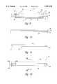
- FIG. 1is a side cross-sectional view of a semiconductor structure according to a first embodiment of the invention.
- FIG. 2Ais a cross-sectional view taken along the line A-A' of FIG. 1.
- FIG. 2Bis a cross-sectional view taken along the line B-B' of FIG. 1.
- FIG. 3is a cross-sectional view at a first point in one embodiment of a method for forming the semiconductor structure of FIG. 1.
- FIG. 4is a cross-sectional view at a second point in the method.
- FIG. 5is a cross-sectional view taken along lines C-C' of FIG. 4 at a third point in the method.
- FIG. 6is a cross-sectional view taken at a fourth point in the method.
- FIG. 7is a cross-sectional view taken along lines D-D' at a fifth point in the method.
- FIG. 8is a cross-sectional view taken at a sixth point in the method.
- FIG. 9is a side cross-sectional view of a semiconductor structure according to a second embodiment of the invention.
- FIG. 10is a cross-sectional view taken at a first point in one embodiment of a method for forming the semiconductor structure of FIG. 9.
- FIG. 11is a top view taken at a second point in the method.
- FIG. 12is a top view taken at a third point in the method.
- FIG. 13Ais a cross-sectional view taken along lines A-A' of FIG. 12 at a fourth point in the method.
- FIG. 13Bis a cross-sectional view taken along lines B-B' of FIG. 12 at the fourth point in the method.
- FIG. 14is a cross-sectional view taken along lines B-B' of FIG. 12 at a fifth point in the method.
- FIG. 15is a cross-sectional view taken along lines A-A' of FIG. 12 at the fifth point in the method.
- FIG. 16Ais a cross-sectional view taken along lines A-A' of FIG. 12 at a sixth point in the method.
- FIG. 16Bis a cross-sectional view taken along lines B-B' at the sixth point in the method.
- FIG. 17Ais a cross-sectional view taken along lines A-A' of FIG. 12 at a seventh point in the method.
- FIG. 17Bis a cross-sectional view taken along lines B-B' at the seventh point in the method.
- FIG. 18is a cross-sectional view taken along lines B-B' of FIG. 12 at an eighth point in the method.
- FIG. 19is a cross-sectional view taken along lines B-B' of FIG. 12 at a ninth point in the method.
- FIG. 20is a cross-sectional view taken along lines B-B' at a tenth point in the method.
- FIG. 21is a cross-sectional view taken along lines B-B' of FIG. 12 at an eleventh point in the method.
- FIG. 22is a block diagram of a memory device that incorporates one or both of the semiconductor structures of FIGS. 1 and 9, respectively.
- FIG. 23is a block diagram of an electronic system that incorporates the memory device of FIG. 22.
- FIG. 1is a side cross-sectional view of one embodiment of a semiconductor structure 10, which is part of an integrated circuit such as a memory device.
- the structure 10includes an optical waveguide, i.e., optical path, 12, which is formed in a substrate 14.
- the substrate 14is formed from a semiconductor material such as silicon.
- First and second circuits 16 and 18are formed in a semiconductor layer 20, which is disposed on the substrate 14.
- the circuits 16 and 18include respective transistors, and the layer 20 is an epitaxial layer of silicon.
- Optical-to-electrical couplers 22 and 24are electrically insulated from the substrate by sidewalls 25 and 27, respectively, and couple the first and second circuits 16 and 18 to the optical path 12 via electrical conductors 26 and 28, respectively.
- the couplers 22 and 24comprise respective diodes that act as either or both a photodiode and a light-emitting diode, as discussed below.
- An insulator layer 30is disposed between the substrate 14 and the layer 20, and isolation regions 32 may extend through the layer 20 to the insulator layer 30. In such in an embodiment, the layer 30 and the regions 32 merge to provide a silicon-on-insulator (SOI) structure that includes electrically isolated islands of the semiconductor layer 20 where circuitry can be formed.
- SOIsilicon-on-insulator
- the substrate 14is made from a semiconductor material
- one or both of the first and second circuits 16 and 18may be formed in the substrate 14.
- one or both of the circuits 16 and 18can respectively have a portion formed in the substrate 14 and a portion formed in the semiconductor layer 20.
- FIG. 2Ais a cross-sectional view of the semiconductor structure 10 taken along lines A-A' of FIG. 1.
- FIG. 2Bis a cross-sectional view of the semiconductor structure 10 taken along lines B-B' of FIG. 1.
- the optical path 12includes a reflective outer shell 34, which reduces leakage of the optical signal into the substrate 14.
- the shell 34is a thin layer of a refractory metal such as tungsten.
- the optical path 12also includes a cladding 36 and a core 38, which is surrounded by the cladding 36.
- the insulator layer 30 and the cladding 36include an oxide and thus merge to form a continuous region
- the core 38includes phosphorous-doped silicon glass (PSG). Because the cladding 36 and the core 38 have sufficiently different indexes of refraction, the optical waves are contained within the path 12 with little or no leakage. Furthermore, as discussed above, the reflective properties of the shell 34 serve to further reduce such losses.
- a diodesuch as the diodes 22 and 24, will luminesce when biased to operate in an avalanche mode (light-emitting diode). It is also known that the luminescing efficiency can be improved if the junction of the diode is doped n+/p+ and is abrupt. Furthermore, it is known that a reverse-biased diode has a dark current in the femtoamp (fA) range, but that when exposed to light, the current through the reverse-biased diode increases by many orders of magnitude (photodiode).
- fAfemtoamp
- the diodes 22 and 24are each respectively biased as either a photodiode or a light-emitting diode, depending upon the direction of the signal propagation. For example purposes, the operation will be discussed when the circuit 16 generates a signal that is to be received by the circuit 18.
- the circuit 16generates an electrical signal that modulates the luminescence of, and thus the optical signal generated by, the diode 22, which is biased to operate as a light-emitting diode.
- the substrate 14is biased at a negative voltage, for example between -1V and -3V, such that a relatively low-voltage signal from the circuit 16 can cause the diode 22 to luminesce.
- biasing the substrate 14 at a negative voltagemay also lower the diode-junction breakdown voltage through its gating effect on the n+/p+ junction.
- the sidewalls 25 and 27can be made thinner, for as the thickness of the sidewall decreases, the gating effect increases.
- the substrate 14may be biased at ground, and the circuit 16 generates a higher-voltage signal.
- the diode 24which is reverse-biased to operate as a photodiode, receives the optical signal and modulates a current in response thereto.
- the circuit 18then converts the modulated current into the voltage signal that was transmitted by the circuit 16.
- the transmission speed of the optical signaldepends on the photoemission efficiency of the light-emitting diode 22 (or 24, depending upon the direction of transmission), the transmission efficiency of the optical path 12, and the detection efficiency of the photo diode 24 (or 22).
- the emission and detection efficiencies of the diodes 22 and 24can be conventionally adjusted to suit the particular application.
- the transmission losses that occur in the path 12are a geometric function of the path length. Therefore, the relatively short length of the path 12, as compared to the lengths of conventional fiber optic cables, serves to significantly limit the transmission losses.
- different varieties of materialscan be used for the shell 34, cladding 36, and core 38 to conventionally adjust the transmission characteristics of the optical path 12.
- circuitrysuch as the circuits 16 and 18, can be disposed over the trenches 42 and 44, the trenches do not significantly reduce the amount of die area available for building circuits.
- the optical paths 12take up very little, if any, extra die area.
- each path 12is separated from other paths 12 by the regions of the opaque substrate 14, there is little if any cross-talk between or losses that occur in the optical paths 12.
- the reflective shell 34also aids in reducing cross-talk and losses by reflecting incident optical energy back into the path 12.
- FIGS. 3-8are cross-sectional views that illustrate one embodiment of a method for forming the semiconductor structure 10 of FIGS. 1-2B.
- a conventional oxide-nitride pad structure 40is formed on the substrate 14.
- the pad 40is conventionally masked and etched to remove the portions of the pad 40 that are over the regions of the substrate 14 where the optical paths 12 are to be formed.
- the exposed regions of the substrate 14are etched to form trenches 42 and 44, which in one embodiment have depths of approximately 0.4 microns ( ⁇ m) below the substrate 14 surface. For clarity, only two trenches are shown, it being understood that there may be more or fewer trenches.
- a layer 46 of a refractory metalis conventionally deposited by chemical-vapor deposition (CVD) to line the trenches 42 and 44.
- the layer 46includes tungsten, and is approximately 10 nanometers (nm) thick.
- an insulator layer 48is conventionally CVD deposited on the layer 46.
- the portions of the layer 48 that are within the trenches 42 and 44will form portions of the cladding 36 (FIG. 2B).
- the layer 48includes silicon dioxide and is approximately 60 nm thick.
- a layer 50 of phosphorous-doped silicon glass (PSG)is conventionally CVD deposited on the layer 48 to fill the trenches 42 and 44. Portions of the layer 50 that are in the trenches 42 and 44 will be used to form the core 38 (FIG. 2B).
- the specific characteristics of the PSG layer 50, such as the doping level,can be conventionally varied to tailor the light-transmission characteristics of the optical paths 12 (FIG. 1).
- the PSG layer 50 and the insulator layer 48are conventionally chemically and mechanically polished (CMP) back to the layer 46, which acts as a polish stop.
- CMPchemically and mechanically polished
- the layers 48 and 50may be removed by other conventional means such as etching.
- the layer 46is anisotropically etched until only the portions that line the trenches 42 and 44 remain. These remaining portions of the layer 46 form the outer shells 34 of the respective optical paths 12 (FIG. 2B).
- the PSG layer 50is conventionally recessed in the trenches 42 and 44 to form the respective cores 38.
- the layer 50is etched to a depth of approximately 80 nm below the substrate surface.
- the remaining portions of the layer 48 in the trenches 42 and 44may also be removed to the same or a lesser depth to form portions of the respective cladding regions 36.
- an insulator layeris conventionally CVD deposited to fill the trenches 42 and 44.
- the layeris then conventionally removed from the pad structure 40 to form the remaining portions of the cladding regions 36.
- the layerincludes silicon dioxide and is conventionally polished back to the pad structure 40.
- FIGS. 5 and 6are cross-sectional views of the trench 42 taken along lines C-C' of FIG. 4. Although only trench 42 is shown for clarity, it is understood that process for the trench 44 proceeds in a similar manner.
- a mask(not shown) is conventionally formed on the pad structure 40 and over the trench 42.
- the maskexposes regions 53 of the trench 42 where the diodes 22 and 24 (FIG. 1) are to be formed.
- the exposed regions 53are the end regions of the trench 42. For clarity, only one such region 53 is shown in FIGS. 5 and 6.
- the cladding 36 and the core 38are anisotropically etched back to the shell 34 in the exposed regions 53 of the trench 42.
- the exposed portions of the shell 34 in the regions 53are anisotropically etched so that the portions on the trench bottom are removed and the portions on the trench 42 sidewalls remain.
- an insulating layer 54is conventionally formed to line the bottom and sidewalls of the exposed trench regions.
- the layer 54includes silicon dioxide that is conventionally CVD deposited to a thickness of approximately 10 nm or less.
- the layer 54is anisotropically etched so that the portions on the trench bottom are removed and the portions along the trench sidewalls remain.
- the structureis now as shown in FIG. 5.
- epitaxial p+ siliconis then conventionally grown from the exposed regions of the substrate 14 at the bottom of the trench 42 until it fills the trench openings.
- the exposed substrate regionsact as seed regions for the epitaxial silicon.
- the doping concentration of the epitaxial siliconis conventionally graded from approximately 10 19 atoms/cm 3 at the trench bottom to approximately 10 17 atoms/cm 3 at the trench top. The lower doping concentration at the top facilitates the n-type counter doping of the epitaxial silicon to form the diode 22 as discussed below.
- the epitaxial siliconis conventionally polished or otherwise removed back to the pad structure 40.
- the epitaxial siliconis conventionally recessed below the surface of the substrate 14, in one embodiment to a depth of approximately 100 nm.
- the recessed epitaxial siliconis implanted with an n-type dopant to form the n+/p+ diode 22.
- the n+ regionhas a doping concentration of approximately 10 19 atoms/cm 3 .
- the insulator layer 30is conventionally formed to fill the trench and to form an insulator cap on the diode 22.
- the layer 30includes silicon dioxide that is conventionally CVD deposited and polished back to the pad 40.
- the layer 30merges with the cladding 36 to form an approximately continuous cladding-insulator region.
- FIGS. 7 and 8are cross-sectional views taken along lines D-D' of FIG. 6.
- the regions of the pad 40 that are aligned with the active areas to be later formed in the layer 20are conventionally removed.
- the pad 40is conventionally masked and the exposed regions are etched away.
- the exposed regions of the substrate 14are conventionally recessed to form regions 56.
- the regions 56are conventionally etched to a depth of approximately 200 nm below the substrate 14 surface.
- an insulator layer 58is conventionally formed to fill in the recessed regions 56 and to fill any remaining discontinuities in the trenches 42 and 44.
- the layer 58includes silicon dioxide that is conventionally CVD deposited and polished back to the remaining regions of the pad 40.
- the pad 40is conventionally removed to expose portions 60 of the substrate 14 that are between the insulator-filled regions 56 and the trenches 42 and 44.
- an epitaxial silicon layer 62is grown to a thickness that is sufficient for the layer 62 to completely cover the regions 60, the insulator-filled regions 56, and the trenches 42 and 44.
- the layer 62is grown to a thickness of approximately 0.5 ⁇ m. This thickness is sufficient where the widths of the regions 56 and the trenches 42 and 44, and the combined widths of any regions 56 and trenches 42 or 44 that are contiguous, are 0.4 ⁇ m or less.
- the layer 62is conventionally polished to provide a planar surface for subsequent conventional device processing.
- the isolation regions 32may be conventionally formed, such as by conventional silicon trench isolation (STI), to define the electrically isolated regions 20 (FIG. 1) of the layer 62. Conventional techniques may then be used to form the conductors 26 and 28 (FIG. 1).
- STIsilicon trench isolation
- FIG. 9is a cross-sectional view of a semiconductor structure 70 according to a second embodiment of the invention.
- An optical path 72which is similar to the optical path 12 of FIG. 1, is disposed in a trench 73 of a substrate 74.
- the path 72includes reflectors 76 and 78 for deflecting optical signals to and from diodes 80 and 82, which are similar to the diodes 22 and 24 of FIG. 1 and which are coupled to or form part of circuits 84 and 86, respectively.
- the circuits 84 and 86are disposed in a semiconductor layer 88, which is disposed on an insulator layer 90.
- the layer 90is transparent to allow optical communication between the reflectors 76 and 78 and the diodes 80 and 82, respectively.
- the layer 90is opaque, and optical pathways are disposed in the layer 90 to allow such optical communication.
- the substrate 74is made from a semiconductor material
- one or both of the circuits 84 an 86may be disposed in the substrate 74.
- one or both of the circuits 84 and 86can respectively have a portion formed in the substrate 74 and a portion formed in the semiconductor layer 88.
- the structure 70operates similarly to the structure 10 of FIG. 1.
- the reflectors 76 and 78are shown as disposed at the ends of the optical path 72, in another embodiment they are disposed in mid regions of the path 72 and are partially reflective such that each one reflects a portion of the optical signal to a diode and lets another portion of the signal continue propagating along the path 72 to one or more additional reflectors (not shown in FIG. 9). In this way, a single path 72 can optically couple more than two circuits.
- FIGS. 10 and 13A-21are cross-sectional side views and FIGS. 11-12 are top views that show one embodiment of a method for forming the structure 70 of FIG. 9.
- the substrate 74which in one embodiment is a silicon substrate, has an orientation.
- the substrate 24is horizontally oriented such that the substrate surface lies in the ⁇ 100> plane.
- a first insulator layer 92is then conventionally formed on the substrate 74.
- the layer 92includes a pad oxide that is thermally grown to a thickness of approximately 10 nm.
- a second insulator layer 94is conventionally formed on the layer 92.
- the layer 94includes silicon nitride that is conventionally CVD deposited to a thickness of approximately 0.5 ⁇ m.
- a third insulator layer 96is conventionally formed on the layer 94.
- the layer 96includes an oxide that is conventionally CVD deposited to a thickness of approximately 0.1 ⁇ m.
- a first maskis formed to expose a region 98 of the layer 96 where the trench 73 is to be formed, and the exposed region 98 of the third insulator layer 96 is conventionally removed.
- the width of the region 98is approximately 3.0 ⁇ m, and the length is approximately two minimum images longer than the desired length of the optical path 72, one minimum image longer on each end.
- a second mask(not shown in FIG. 11) is formed to cover the ends 100 and 102 of the region 98.
- the uncovered regions of the layers 92 and 94 within the region 98are then conventionally removed to expose the substrate 74, but the layers 92 and 94 are not removed in the regions 100 and 102.
- both the first and second masksare removed.
- FIG. 12 and 13A-13Bare cross-sectional views taken along lines A-A' and B-B', respectively, of FIG. 12, the exposed region of the substrate 74 is subjected to a conventional orientation-dependent etch (ODE) to bring out the 45° planes (with respect to the substrate surface) in the exposed region of the substrate 74.
- ODEorientation-dependent etch
- ODE etchantsare formulated to reveal one of the planes of the silicon crystal lattice. Thus, where revealing a plane requires the breaking of one molecular bond, a weaker ODE etchant is used, and where revealing a plane requires the breaking of multiple molecular bonds, a stronger ODE etchant is used, the etchant strength being dependent upon the number of bonds that must be broken to reveal the desired plane. ODE etching is further discussed in U.S. Pat. No. 3,765,969, entitled “Precision Etching of Semiconductors,” which is incorporated by reference.
- the ODEis continued until a trench 104 is formed to a desired depth, which in one embodiment is approximately equal to the width of the region 98.
- the trench 104has sloped sides and ends that lie in respective ⁇ 110> planes.
- the trench sidesundercut both the layers 94 and 96, and the trench ends undercut only the layer 94.
- the sloped sides and endsare formed by an ODE, they are crystallographic surfaces, i.e., surfaces that are atomically flat or substantially atomically flat.
- the exposed portions of the layer 92 above the trench 104may be removed by the ODE or may be removed in a separate etching step that is performed sometime after the ODE.
- the bottom of the trench 104is anisotropically etched a desired depth, which in one embodiment is approximately 1 ⁇ m, below the bottoms of the sloped sides and ends.
- FIG. 15is a cross-sectional view taken along lines A-A' of FIG. 12, the exposed regions of the layer 94 that overhang the ends of the trench 104 (FIG. 13A) are directionally etched while the layer 96 acts as a mask to prevent etching of the unexposed regions of the layer 94.
- an insulator layer 106is formed to line the trench 104.
- the layer 106includes an oxide that is thermally grown to a thickness of approximately 10 nm.
- the layer 108includes polysilicon that is conventionally CVD deposited and then conventionally polished back to the surface of the layer 96.
- FIGS. 17A-17Bwhich are cross-sectional views taken along A-A' and B-B', respectively, of FIG. 12, using the layer 106 as an etch stop, a conventional anisotropic etch removes the regions of the layer 108 from the bottom and ends of the trench 104, but leaves the regions of the layer 108 that are one the sloped trench sides beneath the layer 94.
- the layer 108is not deposited, and thus the regions over the sloped sides of the trench 104 are not filled with an opaque material. In such an embodiment, these unfilled regions will eventually be filled with the optical material that will form the optical path 72. But an advantage of filling these regions with the opaque layer 108 is that the optical path 72 may be less lossy.
- the bottom of the trench 104is filled with a layer 110.
- the layer 110includes oxide that is conventionally CVD deposited and then is conventionally polished back to the layer 94. In an embodiment where the layer 96 has not been previously removed, the polishing also removes the layer 96.
- the remaining regions of the layer 110are conventionally recessed a predetermined amount.
- the layer 110is etched back with a timed etch to a thickness of approximately 1 ⁇ m at the bottom of the trench 104.
- an insulator layer 112is conventionally formed to line the vertical side walls of the trench 104.
- the layer 112includes an oxide that is conventionally CVD deposited and then is conventionally anisotropically etched. The remaining portions of the layer 112 and the layer 110 merge to form portions of the cladding 113 (FIG. 20) of the optical path 72.
- the etch of the layer 112is timed to prevent removal of the layer 110 from the bottom of the trench 104.
- the layer 114includes a phosphorous-doped glass that is doped with approximately 10% phosphorous and that is conventionally CVD deposited and then conventionally polished back to the layer 94.
- the layer 114is recessed to form a core 115, and the layers 92 and 94 are removed.
- the layer 94includes a nitride pad
- the layer 114is conventionally recess etched approximately 1.5 ⁇ m below the surface of the substrate 74
- the layer 94is conventionally stripped with phosphoric acid or another etchant
- the layer 92is conventionally removed.
- the insulator layer 90(FIG. 9) is formed to fill in the recessed portion of the trench 104 and thus merge with the layer 112 to form the remaining regions of the cladding 1 13, and to cover the surface of the substrate 74.
- the layer 90includes an oxide that is conventionally CVD deposited to a thickness of approximately 1 ⁇ m.
- regions of the layer 90are conventionally removed to expose regions 122 of the substrate 74.
- regions of the layer 90remain over the ends of the trench 104 to form optical paths between the reflectors 76 and 78 and the diodes 80 and 82, respectively (FIG. 9).
- a region of the layer 90may remain over the entire optical path 72 to allow the formation of other circuits thereover.
- a semiconductor layer 124is formed on the substrate 74 and on the remaining portions of the layer 90.
- the layer 124includes an epitaxial silicon layer that is grown to a thickness of approximately 1 ⁇ m from the surface of the layer 90.
- An SOI structurecan then be formed in a manner similar to that discussed above in conjunction with FIG. 8.
- the diodes 80 and 82are formed in a manner similar to that described above in conjunction with FIGS. 1-8 for the diodes 22 and 24, except that the diodes 80 and 82 are oriented parallel to the substrate 74 surface so that the p+/n+ junctions can receive and transmit optical signals to and from the respective reflectors 76 and 78, which reflect optical signals between the optical path 72 and the diodes 80 and 82, respectively.
- the layer 90is transparent, the optical signals easily propagate therethrough between the respective reflectors 76 and 78 and the diodes 80 and 82, respectively. Although a transparent layer 90 may cause some losses, it is typically thin enough such that these losses will be negligible. In embodiments where the layer 90 is opaque, vias are formed and filled with a transparent material to allow optical transmission between the respective reflectors 76 and 78 and the diodes 80 and 82.
- FIG. 22is a block diagram of a memory circuit 130, which can include one or both of the semiconductor structures 10 and 70 of FIGS. 1 and 9, respectively.
- the memory circuit 130includes and address register 132, which receives and address from an ADDRESS bus.
- a control logic circuit 134receives a clock (CLK) signal, and receives clock enable (CKE), chip select (CS), row address strobe (RAS), column address strobe (CAS), and write enable (WE) signals from the COMMAND bus, and communicates with the other circuits of the memory device 130.
- a row address multiplexer 136receives the address signal from the address register 132 and provides the row address to the row-address latch-and-decode circuits 138a and 138b for the memory bank 140a or 140b, respectively.
- the row-address latch-and-decode circuits 138a and 138bactivate the word lines of the addressed rows of memory cells in the memory banks 140a and 140b, respectively.
- Read/write circuits 142a and 142bread data from the addressed memory cells in the memory banks 140a and 140b, respectively, during a read cycle, and write data to the addressed memory cells during a write cycle.
- a column-address latch-and-decode circuit 144receives the address from the address register 132 and provides the column address of the selected memory cells to the read/write circuits 142a and 142b.
- the address register 132, the row-address multiplexer 136, the row-address latch-and-decode circuits 138a and 138b, and the column-address latch-and-decode circuit 144can be collectively referred to as an address decoder.
- a data input/output (I/O) circuit 146includes a plurality of input buffers 148. During a write cycle, the buffers 148 receive and store data from the DATA bus, and the read/write circuits 142a and 142b provide the stored data to the memory banks 140a and 140b, respectively.
- the data I/O circuit 146also includes a plurality of output drivers 150. During a read cycle, the read/write circuits 142a and 142b provide data from the memory banks 140a and 140b, respectively, to the drivers 150, which in turn provide this data to the DATA bus.
- a refresh counter 152stores the address of the row of memory cells to be refreshed either during a conventional auto-refresh mode or self-refresh mode. After the row is refreshed, a refresh controller 154 updates the address in the refresh counter 152, typically by either incrementing or decrementing the contents of the refresh counter 152 by one. Although shown separately, the refresh controller 154 may be part of the control logic 134 in other embodiments of the memory device 130.
- the memory device 130may also include an optional charge pump 156, which steps up the power-supply voltage V DD to a voltage V DDP .
- the pump 156generates V DDP approximately 1-1.5 V higher than V DD .
- the memory circuit 130may also use V DDP to conventionally overdrive selected internal transistors.
- FIG. 23is a block diagram of an electronic system 160, such as a computer system, that incorporates the memory circuit 130 of FIG. 22.
- the system 160includes computer circuitry 162 for performing computer functions, such as executing software to perform desired calculations and tasks.
- the circuitry 162typically includes a processor 164 and the memory circuit 130, which is coupled to the processor 164.
- One or more input devices 166such as a keyboard or a mouse, are coupled to the computer circuitry 162 and allow an operator (not shown) to manually input data thereto.
- One or more output devices 168are coupled to the computer circuitry 162 to provide to the operator data generated by the computer circuitry 162. Examples of such output devices 168 include a printer and a video display unit.
- One or more data-storage devices 170are coupled to the computer circuitry 162 to store data on or retrieve data from external storage media (not shown). Examples of the storage devices 170 and the corresponding storage media include drives that accept hard and floppy disks, tape cassettes, and compact disk read-only memories (CD-ROMs).
- the computer circuitry 162includes address data and command buses and a clock line that are respectively coupled to the ADDRESS, DATA, and COMMAND buses, and the CLK line of the memory device 130.
Landscapes
- Physics & Mathematics (AREA)
- General Physics & Mathematics (AREA)
- Optics & Photonics (AREA)
- Engineering & Computer Science (AREA)
- Microelectronics & Electronic Packaging (AREA)
- Optical Integrated Circuits (AREA)
Abstract
Description
Claims (79)
Priority Applications (1)
| Application Number | Priority Date | Filing Date | Title |
|---|---|---|---|
| US08/965,143US5987196A (en) | 1997-11-06 | 1997-11-06 | Semiconductor structure having an optical signal path in a substrate and method for forming the same |
Applications Claiming Priority (1)
| Application Number | Priority Date | Filing Date | Title |
|---|---|---|---|
| US08/965,143US5987196A (en) | 1997-11-06 | 1997-11-06 | Semiconductor structure having an optical signal path in a substrate and method for forming the same |
Publications (1)
| Publication Number | Publication Date |
|---|---|
| US5987196Atrue US5987196A (en) | 1999-11-16 |
Family
ID=25509515
Family Applications (1)
| Application Number | Title | Priority Date | Filing Date |
|---|---|---|---|
| US08/965,143Expired - LifetimeUS5987196A (en) | 1997-11-06 | 1997-11-06 | Semiconductor structure having an optical signal path in a substrate and method for forming the same |
Country Status (1)
| Country | Link |
|---|---|
| US (1) | US5987196A (en) |
Cited By (98)
| Publication number | Priority date | Publication date | Assignee | Title |
|---|---|---|---|---|
| US6147366A (en)* | 1999-02-08 | 2000-11-14 | Intel Corporation | On chip CMOS optical element |
| US6222974B1 (en)* | 1998-07-30 | 2001-04-24 | Seiichi Nagata | Optical waveguide and manufacturing method thereof |
| WO2001031375A1 (en)* | 1999-10-22 | 2001-05-03 | Teraconnect Inc. | Wafer scale integration and remoted subsystems using opto-electronic transceivers |
| US6263140B1 (en)* | 1996-12-17 | 2001-07-17 | Siemens Aktiengesellschaft | Optoelectronic module |
| US6393169B1 (en)* | 1997-12-19 | 2002-05-21 | Intel Corporation | Method and apparatus for providing optical interconnection |
| US20020072253A1 (en)* | 2000-02-10 | 2002-06-13 | Motorola, Inc. | Method of removing an amorphous oxide from a monocrystalline surface |
| US20030026310A1 (en)* | 2001-08-06 | 2003-02-06 | Motorola, Inc. | Structure and method for fabrication for a lighting device |
| US20030036224A1 (en)* | 2001-08-15 | 2003-02-20 | Motorola, Inc. | Method for manufacturing a substantially integral monolithic apparatus including a plurality of semiconductor materials |
| US20030041624A1 (en)* | 2001-09-06 | 2003-03-06 | Jongik Won | Method for performing a deep trench etch for a planar lightwave circuit |
| WO2003009024A3 (en)* | 2001-07-20 | 2003-06-05 | Motorola Inc | Optical waveguide trenches in composite integrated circuits |
| US20030113949A1 (en)* | 2001-08-06 | 2003-06-19 | Motorola, Inc. | Structure and method for fabrication for a solid-state lightning device |
| US20030156778A1 (en)* | 2000-07-27 | 2003-08-21 | Laval Suzanne Colette Marion | Optical interconnection system in a microelectronic circuit produced on a soi substrate |
| US6657272B2 (en)* | 2002-04-19 | 2003-12-02 | Triquint Technology Holding Co. | Off-axis silicon substrate for optimized optical coupling |
| US20040012041A1 (en)* | 2002-07-22 | 2004-01-22 | Applied Materials, Inc. | Optical ready wafers |
| US20040013338A1 (en)* | 2002-07-22 | 2004-01-22 | Applied Materials, Inc. | Optical ready substrates |
| US6693298B2 (en) | 2001-07-20 | 2004-02-17 | Motorola, Inc. | Structure and method for fabricating epitaxial semiconductor on insulator (SOI) structures and devices utilizing the formation of a compliant substrate for materials used to form same |
| US20040042722A1 (en)* | 2002-08-29 | 2004-03-04 | Micron Technology, Inc. | Resistive heater for thermo optic device |
| US6709989B2 (en) | 2001-06-21 | 2004-03-23 | Motorola, Inc. | Method for fabricating a semiconductor structure including a metal oxide interface with silicon |
| US20040057687A1 (en)* | 2002-08-29 | 2004-03-25 | Micron Technology, Inc. | Resonator for thermo optic device |
| WO2004010192A3 (en)* | 2002-07-22 | 2004-04-22 | Applied Materials Inc | Optical-ready substrates with optical waveguide circuits and microelectronic circuits |
| US20040097096A1 (en)* | 2002-11-19 | 2004-05-20 | Yong Liang | Method for fabricating semiconductor structures and devices on vicinal substrates using a low temperature, low pressure, alkaline earth metal-rich process |
| US20040114853A1 (en)* | 2002-07-22 | 2004-06-17 | Applied Materials, Inc. | Optical ready substrates |
| US20040129949A1 (en)* | 2001-05-17 | 2004-07-08 | Shrenik Deliwala | Hybrid active and electronic circuit with evanescent coupling |
| US20040188379A1 (en)* | 2003-03-28 | 2004-09-30 | Cabot Microelectronics Corporation | Dielectric-in-dielectric damascene process for manufacturing planar waveguides |
| US6806202B2 (en) | 2002-12-03 | 2004-10-19 | Motorola, Inc. | Method of removing silicon oxide from a surface of a substrate |
| US20050031284A1 (en)* | 2002-08-29 | 2005-02-10 | Micron Technology, Inc., Clarendon Photonics | Waveguide for thermo optic device |
| US6855992B2 (en) | 2001-07-24 | 2005-02-15 | Motorola Inc. | Structure and method for fabricating configurable transistor devices utilizing the formation of a compliant substrate for materials used to form the same |
| US20050053383A1 (en)* | 2003-05-29 | 2005-03-10 | Applied Materials, Inc. | Serial routing of optical signals |
| US20050054130A1 (en)* | 2003-05-29 | 2005-03-10 | Applied Materials, Inc. | Maskless Fabrication of waveguide mirrors |
| US20050072979A1 (en)* | 2002-07-22 | 2005-04-07 | Applied Materials, Inc. | Optical-ready wafers |
| US6885065B2 (en) | 2002-11-20 | 2005-04-26 | Freescale Semiconductor, Inc. | Ferromagnetic semiconductor structure and method for forming the same |
| US20050132159A1 (en)* | 2002-08-16 | 2005-06-16 | Jeddeloh Joseph M. | Memory hub bypass circuit and method |
| US20050146943A1 (en)* | 2003-08-28 | 2005-07-07 | Jeddeloh Joseph M. | Memory module and method having on-board data search capabilities and processor-based system using such memory modules |
| US6916717B2 (en) | 2002-05-03 | 2005-07-12 | Motorola, Inc. | Method for growing a monocrystalline oxide layer and for fabricating a semiconductor device on a monocrystalline substrate |
| US20050177677A1 (en)* | 2004-02-05 | 2005-08-11 | Jeddeloh Joseph M. | Arbitration system having a packet memory and method for memory responses in a hub-based memory system |
| US6963090B2 (en) | 2003-01-09 | 2005-11-08 | Freescale Semiconductor, Inc. | Enhancement mode metal-oxide-semiconductor field effect transistor |
| US6965128B2 (en) | 2003-02-03 | 2005-11-15 | Freescale Semiconductor, Inc. | Structure and method for fabricating semiconductor microresonator devices |
| US6980042B2 (en) | 2004-04-05 | 2005-12-27 | Micron Technology, Inc. | Delay line synchronizer apparatus and method |
| US6992321B2 (en) | 2001-07-13 | 2006-01-31 | Motorola, Inc. | Structure and method for fabricating semiconductor structures and devices utilizing piezoelectric materials |
| US7005717B2 (en) | 2000-05-31 | 2006-02-28 | Freescale Semiconductor, Inc. | Semiconductor device and method |
| US7019332B2 (en) | 2001-07-20 | 2006-03-28 | Freescale Semiconductor, Inc. | Fabrication of a wavelength locker within a semiconductor structure |
| US7045815B2 (en) | 2001-04-02 | 2006-05-16 | Freescale Semiconductor, Inc. | Semiconductor structure exhibiting reduced leakage current and method of fabricating same |
| US7067856B2 (en) | 2000-02-10 | 2006-06-27 | Freescale Semiconductor, Inc. | Semiconductor structure, semiconductor device, communicating device, integrated circuit, and process for fabricating the same |
| US7101725B2 (en) | 2003-07-23 | 2006-09-05 | Applied Materials, Inc. | Solution to thermal budget |
| US7107415B2 (en) | 2003-06-20 | 2006-09-12 | Micron Technology, Inc. | Posted write buffers and methods of posting write requests in memory modules |
| US7106611B2 (en) | 2002-09-09 | 2006-09-12 | Micron Technology, Inc. | Wavelength division multiplexed memory module, memory system and method |
| US7105866B2 (en) | 2000-07-24 | 2006-09-12 | Freescale Semiconductor, Inc. | Heterojunction tunneling diodes and process for fabricating same |
| US7117316B2 (en) | 2002-08-05 | 2006-10-03 | Micron Technology, Inc. | Memory hub and access method having internal row caching |
| US7120727B2 (en) | 2003-06-19 | 2006-10-10 | Micron Technology, Inc. | Reconfigurable memory module and method |
| US7120723B2 (en) | 2004-03-25 | 2006-10-10 | Micron Technology, Inc. | System and method for memory hub-based expansion bus |
| US7120743B2 (en) | 2003-10-20 | 2006-10-10 | Micron Technology, Inc. | Arbitration system and method for memory responses in a hub-based memory system |
| US7133991B2 (en) | 2003-08-20 | 2006-11-07 | Micron Technology, Inc. | Method and system for capturing and bypassing memory transactions in a hub-based memory system |
| US7133972B2 (en) | 2002-06-07 | 2006-11-07 | Micron Technology, Inc. | Memory hub with internal cache and/or memory access prediction |
| US7136958B2 (en) | 2003-08-28 | 2006-11-14 | Micron Technology, Inc. | Multiple processor system and method including multiple memory hub modules |
| US7162567B2 (en) | 2004-05-14 | 2007-01-09 | Micron Technology, Inc. | Memory hub and method for memory sequencing |
| US7161227B2 (en) | 2001-08-14 | 2007-01-09 | Motorola, Inc. | Structure and method for fabricating semiconductor structures and devices for detecting an object |
| US7180522B2 (en) | 2000-06-23 | 2007-02-20 | Micron Technology, Inc. | Apparatus and method for distributed memory control in a graphics processing system |
| US7181584B2 (en) | 2004-02-05 | 2007-02-20 | Micron Technology, Inc. | Dynamic command and/or address mirroring system and method for memory modules |
| US7188219B2 (en) | 2004-01-30 | 2007-03-06 | Micron Technology, Inc. | Buffer control system and method for a memory system having outstanding read and write request buffers |
| US20070053643A1 (en)* | 2005-09-01 | 2007-03-08 | Applied Materials, Inc. | Ridge technique for fabricating an optical detector and an optical waveguide |
| US7194593B2 (en) | 2003-09-18 | 2007-03-20 | Micron Technology, Inc. | Memory hub with integrated non-volatile memory |
| US7200024B2 (en)* | 2002-08-02 | 2007-04-03 | Micron Technology, Inc. | System and method for optically interconnecting memory devices |
| US7210059B2 (en) | 2003-08-19 | 2007-04-24 | Micron Technology, Inc. | System and method for on-board diagnostics of memory modules |
| US7213082B2 (en) | 2004-03-29 | 2007-05-01 | Micron Technology, Inc. | Memory hub and method for providing memory sequencing hints |
| US7211852B2 (en) | 2001-01-19 | 2007-05-01 | Freescale Semiconductor, Inc. | Structure and method for fabricating GaN devices utilizing the formation of a compliant substrate |
| US7222197B2 (en) | 2003-07-22 | 2007-05-22 | Micron Technology, Inc. | Apparatus and method for direct memory access in a hub-based memory system |
| US7222213B2 (en) | 2004-05-17 | 2007-05-22 | Micron Technology, Inc. | System and method for communicating the synchronization status of memory modules during initialization of the memory modules |
| US7234070B2 (en) | 2003-10-27 | 2007-06-19 | Micron Technology, Inc. | System and method for using a learning sequence to establish communications on a high-speed nonsynchronous interface in the absence of clock forwarding |
| US7242213B2 (en) | 2003-06-11 | 2007-07-10 | Micron Technology, Inc. | Memory module and method having improved signal routing topology |
| US7254331B2 (en) | 2002-08-09 | 2007-08-07 | Micron Technology, Inc. | System and method for multiple bit optical data transmission in memory systems |
| US7257683B2 (en) | 2004-03-24 | 2007-08-14 | Micron Technology, Inc. | Memory arbitration system and method having an arbitration packet protocol |
| US7260685B2 (en) | 2003-06-20 | 2007-08-21 | Micron Technology, Inc. | Memory hub and access method having internal prefetch buffers |
| US7310748B2 (en) | 2004-06-04 | 2007-12-18 | Micron Technology, Inc. | Memory hub tester interface and method for use thereof |
| US7342276B2 (en) | 2001-10-17 | 2008-03-11 | Freescale Semiconductor, Inc. | Method and apparatus utilizing monocrystalline insulator |
| US7363419B2 (en) | 2004-05-28 | 2008-04-22 | Micron Technology, Inc. | Method and system for terminating write commands in a hub-based memory system |
| US7366864B2 (en) | 2004-03-08 | 2008-04-29 | Micron Technology, Inc. | Memory hub architecture having programmable lane widths |
| US7392331B2 (en) | 2004-08-31 | 2008-06-24 | Micron Technology, Inc. | System and method for transmitting data packets in a computer system having a memory hub architecture |
| US7428644B2 (en) | 2003-06-20 | 2008-09-23 | Micron Technology, Inc. | System and method for selective memory module power management |
| US7447240B2 (en) | 2004-03-29 | 2008-11-04 | Micron Technology, Inc. | Method and system for synchronizing communications links in a hub-based memory system |
| US20080317423A1 (en)* | 2004-09-02 | 2008-12-25 | Ramot At Tel Aviv University Ltd. | Embedded Channels, Embedded Waveguide And Methods Of Manufacturing And Using The Same |
| US7519788B2 (en) | 2004-06-04 | 2009-04-14 | Micron Technology, Inc. | System and method for an asynchronous data buffer having buffer write and read pointers |
| US7590797B2 (en) | 2004-04-08 | 2009-09-15 | Micron Technology, Inc. | System and method for optimizing interconnections of components in a multichip memory module |
| US20090261367A1 (en)* | 2008-04-18 | 2009-10-22 | Spansion Llc | Optical erase memory structure |
| US20100144075A1 (en)* | 2008-12-05 | 2010-06-10 | Electronics And Telecommunications Research Institute | Method of forming optical waveguide |
| US20100155872A1 (en)* | 2008-12-24 | 2010-06-24 | Jeong-Su Park | Image sensor and manufacturing method of image sensor |
| US7788451B2 (en) | 2004-02-05 | 2010-08-31 | Micron Technology, Inc. | Apparatus and method for data bypass for a bi-directional data bus in a hub-based memory sub-system |
| US7805586B2 (en) | 2002-08-29 | 2010-09-28 | Micron Technology, Inc. | System and method for optimizing interconnections of memory devices in a multichip module |
| US20110073875A1 (en)* | 2009-09-30 | 2011-03-31 | Uwe Griebenow | Optical signal transfer in a semiconductor device by using monolithic opto-electronic components |
| US20110136318A1 (en)* | 2009-12-09 | 2011-06-09 | Electronics And Telecommunications Research Institute | Method of manufacturing semiconductor device having optical devices |
| NL2010018A (en)* | 2012-01-04 | 2013-07-09 | Gen Electric | Photodiode arrays and methods of fabrication. |
| US20140043757A1 (en)* | 2012-08-07 | 2014-02-13 | International Business Machines Corporation | Electro-rheological micro-channel anisotropic cooled integrated circuits and methods thereof |
| US8880833B2 (en) | 2003-12-29 | 2014-11-04 | Micron Technology, Inc. | System and method for read synchronization of memory modules |
| US20150048319A1 (en)* | 2013-08-19 | 2015-02-19 | Samsung Display Co., Ltd. | Organic light-emitting display apparatus |
| EP2059841B1 (en)* | 2006-08-10 | 2015-07-08 | Panasonic Corporation | Photoelectric converter |
| US9864136B1 (en)* | 2016-08-09 | 2018-01-09 | Globalfoundries Inc. | Non-planar monolithic hybrid optoelectronic structures and methods |
| US20180217329A1 (en)* | 2015-10-28 | 2018-08-02 | International Business Machines Corporation | Integration of bonded optoelectronics, photonics waveguide and vlsi soi |
| US20220065798A1 (en)* | 2020-08-28 | 2022-03-03 | Juniper Networks, Inc. | Loss monitoring in photonic circuit fabrication |
| US11977258B1 (en)* | 2022-12-29 | 2024-05-07 | Globalfoundries U.S. Inc. | Structure with substrate-embedded arrow waveguide and method |
Citations (41)
| Publication number | Priority date | Publication date | Assignee | Title |
|---|---|---|---|---|
| US3765969A (en)* | 1970-07-13 | 1973-10-16 | Bell Telephone Labor Inc | Precision etching of semiconductors |
| US4015893A (en)* | 1972-10-12 | 1977-04-05 | Kentaro Hayashi, President, University of Tokyo | Compound semiconductor optical integrated circuit having isolation zones for light transmission |
| US4652077A (en)* | 1983-07-01 | 1987-03-24 | U.S. Philips Corporation | Semiconductor device comprising a light wave guide |
| US4755015A (en)* | 1985-07-12 | 1988-07-05 | Matsushita Electric Industrial Co., Ltd. | Monolithic integrated semiconductor device of semiconductor laser and optical waveguide |
| US4820655A (en)* | 1986-02-21 | 1989-04-11 | Kokusai Denshin Denwa Kabushiki Kaisha | Method for manufacturing semiconductor optical integrated device with optical waveguide regions |
| US4966430A (en)* | 1988-10-08 | 1990-10-30 | Telefunken Systemtechnik Gmbh | Semiconductor circuit |
| US4999686A (en)* | 1988-06-24 | 1991-03-12 | U.S. Philips Corporation | Semiconductor device comprising an integrated optical guide, which has at least one rectilinear part and one curved part |
| US5159700A (en)* | 1984-01-16 | 1992-10-27 | Texas Instruments Incorporated | Substrate with optical communication systems between chips mounted thereon and monolithic integration of optical I/O on silicon substrates |
| US5170448A (en)* | 1992-01-06 | 1992-12-08 | Motorola, Inc. | Optical waveguide apparatus and method for partially collecting light |
| US5280189A (en)* | 1990-04-09 | 1994-01-18 | Siemens Aktiengesellschaft | Semiconductor element with a silicon layer |
| US5360982A (en)* | 1991-10-08 | 1994-11-01 | U.S. Philips Corporation | Optoelectronic semiconductor having a groove-shaped waveguide |
| US5371818A (en)* | 1993-08-12 | 1994-12-06 | At&T Corp. | Integrated optical circuit and methods for connecting such circuits to glass fibers |
| US5394490A (en)* | 1992-08-11 | 1995-02-28 | Hitachi, Ltd. | Semiconductor device having an optical waveguide interposed in the space between electrode members |
| US5452383A (en)* | 1993-06-30 | 1995-09-19 | Mitsubishi Denki Kabushiki Kaisha | Optical switch and method for producing the optical switch |
| US5481629A (en)* | 1993-08-31 | 1996-01-02 | Fujitsu Limited | Hybrid optical IC with optical axes at different levels |
| US5485021A (en)* | 1993-06-17 | 1996-01-16 | Shin-Etsu Handotai Co., Ltd. | Semiconductor device with optical waveguides to achieve signal transmission using optical means |
| US5488678A (en)* | 1993-08-03 | 1996-01-30 | Sharp Kabushiki Kaisha | Assembly structure for an optical integrated circuit device |
| US5502779A (en)* | 1991-11-22 | 1996-03-26 | Texas Instruments Incorporated | Integrated optical modulator and waveguide and method |
| US5513288A (en)* | 1992-06-15 | 1996-04-30 | Robert Bosch Gmbh | Optical polymer element for coupling photoelements onto integrated-optical circuits |
| US5513285A (en)* | 1993-06-17 | 1996-04-30 | Oki Electric Industry Co.Ltd. | Compact optical switching module including thin-film heaters and trimmed thick-film fixed resistors |
| US5519803A (en)* | 1993-09-22 | 1996-05-21 | Shin-Etsu Chemical Co., Ltd. | Optical waveguide |
| US5521994A (en)* | 1994-06-29 | 1996-05-28 | Nec Corporation | Semiconductor optical waveguide-integrated light-receiving device |
| US5523557A (en)* | 1994-04-26 | 1996-06-04 | France Telecom | Optoelectronic device integrating a light guide and a photodetector having two diodes arranged side by side on a semiconductor substrate |
| US5526454A (en)* | 1992-04-10 | 1996-06-11 | Robert Bosch Gmbh | Method for producing optical polymer components having integrated fibre-chip coupling by means of casting technology |
| US5534442A (en)* | 1991-05-10 | 1996-07-09 | Northern Telecom Limited | Process of providing uniform photoresist thickness on an opto-electronic device |
| US5546489A (en)* | 1993-08-02 | 1996-08-13 | Sumitomo Electric Industries, Ltd. | Optical link apparatus |
| US5559914A (en)* | 1993-10-19 | 1996-09-24 | Matsushita Electric Industrial Co., Ltd. | Components for optical circuits and method of manufacturing the same |
| US5574806A (en)* | 1993-01-13 | 1996-11-12 | Robert Bosch Gmbh | Hybrid integrated optical circuit and device for emitting light waves |
| US5577139A (en)* | 1995-08-17 | 1996-11-19 | Lucent Technologies Inc. | Integrated-circuit optical network unit |
| US5577138A (en)* | 1995-08-17 | 1996-11-19 | Lucent Technologies Inc. | Integrated-circuit optical network unit |
| US5598490A (en)* | 1993-09-17 | 1997-01-28 | Fujitsu Limited | Dielectric optical waveguide device |
| US5600741A (en)* | 1994-05-11 | 1997-02-04 | Ant Nachrichtentechnik Gmbh | Arrangement for coupling optoelectronic components and optical waveguides to one another |
| US5602672A (en)* | 1995-09-20 | 1997-02-11 | Mitsubishi Denki Kabushiki Kaisha | Light modulator module and method for fabricating light modulator module |
| US5604835A (en)* | 1993-12-27 | 1997-02-18 | Hitachi, Ltd. | Integrated optical waveguide device |
| US5611008A (en)* | 1996-01-26 | 1997-03-11 | Hughes Aircraft Company | Substrate system for optoelectronic/microwave circuits |
| US5621828A (en)* | 1992-09-24 | 1997-04-15 | Interuniversitair Micro-Elektronica Centrum Vzw | Integrated tunable optical filter |
| US5696862A (en)* | 1994-11-17 | 1997-12-09 | Robert Bosch Gmbh | Optical transmitting and receiving device having a surface-emitting laser |
| US5701374A (en)* | 1995-05-12 | 1997-12-23 | Fujitsu Limited | Integrated optical module including a waveguide and a photoreception device |
| US5835646A (en)* | 1995-09-19 | 1998-11-10 | Fujitsu Limited | Active optical circuit sheet or active optical circuit board, active optical connector and optical MCM, process for fabricating optical waveguide, and devices obtained thereby |
| US5848214A (en)* | 1997-07-16 | 1998-12-08 | The United States Of America As Represented By The Secretary Of The Air Force | Optically-guiding multichip module |
| US5883988A (en)* | 1996-05-13 | 1999-03-16 | Fujitsu Limited | Optical module including a photoreception device |
- 1997
- 1997-11-06USUS08/965,143patent/US5987196A/ennot_activeExpired - Lifetime
Patent Citations (41)
| Publication number | Priority date | Publication date | Assignee | Title |
|---|---|---|---|---|
| US3765969A (en)* | 1970-07-13 | 1973-10-16 | Bell Telephone Labor Inc | Precision etching of semiconductors |
| US4015893A (en)* | 1972-10-12 | 1977-04-05 | Kentaro Hayashi, President, University of Tokyo | Compound semiconductor optical integrated circuit having isolation zones for light transmission |
| US4652077A (en)* | 1983-07-01 | 1987-03-24 | U.S. Philips Corporation | Semiconductor device comprising a light wave guide |
| US5159700A (en)* | 1984-01-16 | 1992-10-27 | Texas Instruments Incorporated | Substrate with optical communication systems between chips mounted thereon and monolithic integration of optical I/O on silicon substrates |
| US4755015A (en)* | 1985-07-12 | 1988-07-05 | Matsushita Electric Industrial Co., Ltd. | Monolithic integrated semiconductor device of semiconductor laser and optical waveguide |
| US4820655A (en)* | 1986-02-21 | 1989-04-11 | Kokusai Denshin Denwa Kabushiki Kaisha | Method for manufacturing semiconductor optical integrated device with optical waveguide regions |
| US4999686A (en)* | 1988-06-24 | 1991-03-12 | U.S. Philips Corporation | Semiconductor device comprising an integrated optical guide, which has at least one rectilinear part and one curved part |
| US4966430A (en)* | 1988-10-08 | 1990-10-30 | Telefunken Systemtechnik Gmbh | Semiconductor circuit |
| US5280189A (en)* | 1990-04-09 | 1994-01-18 | Siemens Aktiengesellschaft | Semiconductor element with a silicon layer |
| US5534442A (en)* | 1991-05-10 | 1996-07-09 | Northern Telecom Limited | Process of providing uniform photoresist thickness on an opto-electronic device |
| US5360982A (en)* | 1991-10-08 | 1994-11-01 | U.S. Philips Corporation | Optoelectronic semiconductor having a groove-shaped waveguide |
| US5502779A (en)* | 1991-11-22 | 1996-03-26 | Texas Instruments Incorporated | Integrated optical modulator and waveguide and method |
| US5170448A (en)* | 1992-01-06 | 1992-12-08 | Motorola, Inc. | Optical waveguide apparatus and method for partially collecting light |
| US5526454A (en)* | 1992-04-10 | 1996-06-11 | Robert Bosch Gmbh | Method for producing optical polymer components having integrated fibre-chip coupling by means of casting technology |
| US5513288A (en)* | 1992-06-15 | 1996-04-30 | Robert Bosch Gmbh | Optical polymer element for coupling photoelements onto integrated-optical circuits |
| US5394490A (en)* | 1992-08-11 | 1995-02-28 | Hitachi, Ltd. | Semiconductor device having an optical waveguide interposed in the space between electrode members |
| US5621828A (en)* | 1992-09-24 | 1997-04-15 | Interuniversitair Micro-Elektronica Centrum Vzw | Integrated tunable optical filter |
| US5574806A (en)* | 1993-01-13 | 1996-11-12 | Robert Bosch Gmbh | Hybrid integrated optical circuit and device for emitting light waves |
| US5485021A (en)* | 1993-06-17 | 1996-01-16 | Shin-Etsu Handotai Co., Ltd. | Semiconductor device with optical waveguides to achieve signal transmission using optical means |
| US5513285A (en)* | 1993-06-17 | 1996-04-30 | Oki Electric Industry Co.Ltd. | Compact optical switching module including thin-film heaters and trimmed thick-film fixed resistors |
| US5452383A (en)* | 1993-06-30 | 1995-09-19 | Mitsubishi Denki Kabushiki Kaisha | Optical switch and method for producing the optical switch |
| US5546489A (en)* | 1993-08-02 | 1996-08-13 | Sumitomo Electric Industries, Ltd. | Optical link apparatus |
| US5488678A (en)* | 1993-08-03 | 1996-01-30 | Sharp Kabushiki Kaisha | Assembly structure for an optical integrated circuit device |
| US5371818A (en)* | 1993-08-12 | 1994-12-06 | At&T Corp. | Integrated optical circuit and methods for connecting such circuits to glass fibers |
| US5481629A (en)* | 1993-08-31 | 1996-01-02 | Fujitsu Limited | Hybrid optical IC with optical axes at different levels |
| US5598490A (en)* | 1993-09-17 | 1997-01-28 | Fujitsu Limited | Dielectric optical waveguide device |
| US5519803A (en)* | 1993-09-22 | 1996-05-21 | Shin-Etsu Chemical Co., Ltd. | Optical waveguide |
| US5559914A (en)* | 1993-10-19 | 1996-09-24 | Matsushita Electric Industrial Co., Ltd. | Components for optical circuits and method of manufacturing the same |
| US5604835A (en)* | 1993-12-27 | 1997-02-18 | Hitachi, Ltd. | Integrated optical waveguide device |
| US5523557A (en)* | 1994-04-26 | 1996-06-04 | France Telecom | Optoelectronic device integrating a light guide and a photodetector having two diodes arranged side by side on a semiconductor substrate |
| US5600741A (en)* | 1994-05-11 | 1997-02-04 | Ant Nachrichtentechnik Gmbh | Arrangement for coupling optoelectronic components and optical waveguides to one another |
| US5521994A (en)* | 1994-06-29 | 1996-05-28 | Nec Corporation | Semiconductor optical waveguide-integrated light-receiving device |
| US5696862A (en)* | 1994-11-17 | 1997-12-09 | Robert Bosch Gmbh | Optical transmitting and receiving device having a surface-emitting laser |
| US5701374A (en)* | 1995-05-12 | 1997-12-23 | Fujitsu Limited | Integrated optical module including a waveguide and a photoreception device |
| US5577138A (en)* | 1995-08-17 | 1996-11-19 | Lucent Technologies Inc. | Integrated-circuit optical network unit |
| US5577139A (en)* | 1995-08-17 | 1996-11-19 | Lucent Technologies Inc. | Integrated-circuit optical network unit |
| US5835646A (en)* | 1995-09-19 | 1998-11-10 | Fujitsu Limited | Active optical circuit sheet or active optical circuit board, active optical connector and optical MCM, process for fabricating optical waveguide, and devices obtained thereby |
| US5602672A (en)* | 1995-09-20 | 1997-02-11 | Mitsubishi Denki Kabushiki Kaisha | Light modulator module and method for fabricating light modulator module |
| US5611008A (en)* | 1996-01-26 | 1997-03-11 | Hughes Aircraft Company | Substrate system for optoelectronic/microwave circuits |
| US5883988A (en)* | 1996-05-13 | 1999-03-16 | Fujitsu Limited | Optical module including a photoreception device |
| US5848214A (en)* | 1997-07-16 | 1998-12-08 | The United States Of America As Represented By The Secretary Of The Air Force | Optically-guiding multichip module |
Non-Patent Citations (6)
| Title |
|---|
| Hunt, Charles E. et al., "Electrical and Physical Properties of Rapid-Zone-Recrystallized SOI Made Using a Pulsed Arc Lamp," Abstracts of the 18th (1986 International) Conference on Solid State Devices and Materials, Tokyo, Japan, 1986, pp. 561-565. |
| Hunt, Charles E. et al., Electrical and Physical Properties of Rapid Zone Recrystallized SOI Made Using a Pulsed Arc Lamp, Abstracts of the 18 th ( 1986 International ) Conference on Solid State Devices and Materials, Tokyo, Japan, 1986, pp. 561 565.* |
| Ishiwara, H. et al., "Selective Doping of P Atoms in Lateral Solid Phase Epitaxy of Si Films," Extended Abstracts of the 18th (1986 International) Conference on Solid State Devices and Materials, Tokyo, Japan, 1986, pp. 553-556. |
| Ishiwara, H. et al., Selective Doping of P Atoms in Lateral Solid Phase Epitaxy of Si Films, Extended Abstracts of the 18 th ( 1986 International ) Conference on Solid State Devices and Materials, Tokyo, Japan, 1986, pp. 553 556.* |
| Lu, N.C.C. et al., "A Buried-Trench DRAM Cell Using a Self-Aligned Epitaxy Over Trench Technology," IEDM Digest of Technical Papers, 1998, pp. 588-591. |
| Lu, N.C.C. et al., A Buried Trench DRAM Cell Using a Self Aligned Epitaxy Over Trench Technology, IEDM Digest of Technical Papers, 1998, pp. 588 591.* |
Cited By (229)
| Publication number | Priority date | Publication date | Assignee | Title |
|---|---|---|---|---|
| US6263140B1 (en)* | 1996-12-17 | 2001-07-17 | Siemens Aktiengesellschaft | Optoelectronic module |
| US6393169B1 (en)* | 1997-12-19 | 2002-05-21 | Intel Corporation | Method and apparatus for providing optical interconnection |
| US6222974B1 (en)* | 1998-07-30 | 2001-04-24 | Seiichi Nagata | Optical waveguide and manufacturing method thereof |
| US6147366A (en)* | 1999-02-08 | 2000-11-14 | Intel Corporation | On chip CMOS optical element |
| US6861673B1 (en)* | 1999-02-08 | 2005-03-01 | Intel Corporation | Chip CMOS optical element |
| US7056760B2 (en) | 1999-02-08 | 2006-06-06 | Intel Corporation | On chip CMOS optical element |
| US20050095004A1 (en)* | 1999-02-08 | 2005-05-05 | Ken Drottar | On chip CMOS optical element |
| US6567963B1 (en) | 1999-10-22 | 2003-05-20 | Tera Connect, Inc. | Wafer scale integration and remoted subsystems using opto-electronic transceivers |
| WO2001031375A1 (en)* | 1999-10-22 | 2001-05-03 | Teraconnect Inc. | Wafer scale integration and remoted subsystems using opto-electronic transceivers |
| US20020072253A1 (en)* | 2000-02-10 | 2002-06-13 | Motorola, Inc. | Method of removing an amorphous oxide from a monocrystalline surface |
| US7067856B2 (en) | 2000-02-10 | 2006-06-27 | Freescale Semiconductor, Inc. | Semiconductor structure, semiconductor device, communicating device, integrated circuit, and process for fabricating the same |
| US7005717B2 (en) | 2000-05-31 | 2006-02-28 | Freescale Semiconductor, Inc. | Semiconductor device and method |
| US7180522B2 (en) | 2000-06-23 | 2007-02-20 | Micron Technology, Inc. | Apparatus and method for distributed memory control in a graphics processing system |
| US7105866B2 (en) | 2000-07-24 | 2006-09-12 | Freescale Semiconductor, Inc. | Heterojunction tunneling diodes and process for fabricating same |
| US20030156778A1 (en)* | 2000-07-27 | 2003-08-21 | Laval Suzanne Colette Marion | Optical interconnection system in a microelectronic circuit produced on a soi substrate |
| US7211852B2 (en) | 2001-01-19 | 2007-05-01 | Freescale Semiconductor, Inc. | Structure and method for fabricating GaN devices utilizing the formation of a compliant substrate |
| US7045815B2 (en) | 2001-04-02 | 2006-05-16 | Freescale Semiconductor, Inc. | Semiconductor structure exhibiting reduced leakage current and method of fabricating same |
| US6963118B2 (en)* | 2001-05-17 | 2005-11-08 | Sioptical, Inc. | Hybrid active and electronic circuit with evanescent coupling |
| US20040129949A1 (en)* | 2001-05-17 | 2004-07-08 | Shrenik Deliwala | Hybrid active and electronic circuit with evanescent coupling |
| US6709989B2 (en) | 2001-06-21 | 2004-03-23 | Motorola, Inc. | Method for fabricating a semiconductor structure including a metal oxide interface with silicon |
| US6992321B2 (en) | 2001-07-13 | 2006-01-31 | Motorola, Inc. | Structure and method for fabricating semiconductor structures and devices utilizing piezoelectric materials |
| WO2003009024A3 (en)* | 2001-07-20 | 2003-06-05 | Motorola Inc | Optical waveguide trenches in composite integrated circuits |
| US7019332B2 (en) | 2001-07-20 | 2006-03-28 | Freescale Semiconductor, Inc. | Fabrication of a wavelength locker within a semiconductor structure |
| US6693298B2 (en) | 2001-07-20 | 2004-02-17 | Motorola, Inc. | Structure and method for fabricating epitaxial semiconductor on insulator (SOI) structures and devices utilizing the formation of a compliant substrate for materials used to form same |
| US6855992B2 (en) | 2001-07-24 | 2005-02-15 | Motorola Inc. | Structure and method for fabricating configurable transistor devices utilizing the formation of a compliant substrate for materials used to form the same |
| US20030113949A1 (en)* | 2001-08-06 | 2003-06-19 | Motorola, Inc. | Structure and method for fabrication for a solid-state lightning device |
| US20030026310A1 (en)* | 2001-08-06 | 2003-02-06 | Motorola, Inc. | Structure and method for fabrication for a lighting device |
| US7161227B2 (en) | 2001-08-14 | 2007-01-09 | Motorola, Inc. | Structure and method for fabricating semiconductor structures and devices for detecting an object |
| US20030036224A1 (en)* | 2001-08-15 | 2003-02-20 | Motorola, Inc. | Method for manufacturing a substantially integral monolithic apparatus including a plurality of semiconductor materials |
| US6732550B2 (en)* | 2001-09-06 | 2004-05-11 | Lightwave Microsystems, Inc. | Method for performing a deep trench etch for a planar lightwave circuit |
| US20030041624A1 (en)* | 2001-09-06 | 2003-03-06 | Jongik Won | Method for performing a deep trench etch for a planar lightwave circuit |
| US7342276B2 (en) | 2001-10-17 | 2008-03-11 | Freescale Semiconductor, Inc. | Method and apparatus utilizing monocrystalline insulator |
| US6657272B2 (en)* | 2002-04-19 | 2003-12-02 | Triquint Technology Holding Co. | Off-axis silicon substrate for optimized optical coupling |
| US6916717B2 (en) | 2002-05-03 | 2005-07-12 | Motorola, Inc. | Method for growing a monocrystalline oxide layer and for fabricating a semiconductor device on a monocrystalline substrate |
| US7945737B2 (en) | 2002-06-07 | 2011-05-17 | Round Rock Research, Llc | Memory hub with internal cache and/or memory access prediction |
| US8499127B2 (en) | 2002-06-07 | 2013-07-30 | Round Rock Research, Llc | Memory hub with internal cache and/or memory access prediction |
| US7644253B2 (en) | 2002-06-07 | 2010-01-05 | Micron Technology, Inc. | Memory hub with internal cache and/or memory access prediction |
| US7133972B2 (en) | 2002-06-07 | 2006-11-07 | Micron Technology, Inc. | Memory hub with internal cache and/or memory access prediction |
| US8195918B2 (en) | 2002-06-07 | 2012-06-05 | Round Rock Research, Llc | Memory hub with internal cache and/or memory access prediction |
| US20110219196A1 (en)* | 2002-06-07 | 2011-09-08 | Round Rock Research, Llc | Memory hub with internal cache and/or memory access prediction |
| US20070080414A1 (en)* | 2002-07-22 | 2007-04-12 | Applied Materials, Inc. | Optical ready substrates |
| US20040114853A1 (en)* | 2002-07-22 | 2004-06-17 | Applied Materials, Inc. | Optical ready substrates |
| US20040013338A1 (en)* | 2002-07-22 | 2004-01-22 | Applied Materials, Inc. | Optical ready substrates |
| US7110629B2 (en) | 2002-07-22 | 2006-09-19 | Applied Materials, Inc. | Optical ready substrates |
| US20050072979A1 (en)* | 2002-07-22 | 2005-04-07 | Applied Materials, Inc. | Optical-ready wafers |
| WO2004010192A3 (en)* | 2002-07-22 | 2004-04-22 | Applied Materials Inc | Optical-ready substrates with optical waveguide circuits and microelectronic circuits |
| US20040012041A1 (en)* | 2002-07-22 | 2004-01-22 | Applied Materials, Inc. | Optical ready wafers |
| US7072534B2 (en) | 2002-07-22 | 2006-07-04 | Applied Materials, Inc. | Optical ready substrates |
| US7411807B2 (en) | 2002-08-02 | 2008-08-12 | Micron Technology, Inc. | System and method for optically interconnecting memory devices |
| US7382639B2 (en) | 2002-08-02 | 2008-06-03 | Micron Technology, Inc. | System and method for optically interconnecting memory devices |
| US7200024B2 (en)* | 2002-08-02 | 2007-04-03 | Micron Technology, Inc. | System and method for optically interconnecting memory devices |
| US7289347B2 (en) | 2002-08-02 | 2007-10-30 | Micron Technology, Inc. | System and method for optically interconnecting memory devices |
| US7117316B2 (en) | 2002-08-05 | 2006-10-03 | Micron Technology, Inc. | Memory hub and access method having internal row caching |
| US8954687B2 (en) | 2002-08-05 | 2015-02-10 | Micron Technology, Inc. | Memory hub and access method having a sequencer and internal row caching |
| US7489875B2 (en) | 2002-08-09 | 2009-02-10 | Micron Technology, Inc. | System and method for multiple bit optical data transmission in memory systems |
| US7254331B2 (en) | 2002-08-09 | 2007-08-07 | Micron Technology, Inc. | System and method for multiple bit optical data transmission in memory systems |
| US7047351B2 (en) | 2002-08-16 | 2006-05-16 | Micron Technology, Inc. | Memory hub bypass circuit and method |
| US7149874B2 (en) | 2002-08-16 | 2006-12-12 | Micron Technology, Inc. | Memory hub bypass circuit and method |
| US7415567B2 (en) | 2002-08-16 | 2008-08-19 | Micron Technology, Inc. | Memory hub bypass circuit and method |
| US20050132159A1 (en)* | 2002-08-16 | 2005-06-16 | Jeddeloh Joseph M. | Memory hub bypass circuit and method |
| US7936955B2 (en) | 2002-08-29 | 2011-05-03 | Micron Technology, Inc. | Waveguide for thermo optic device |
| US20110206332A1 (en)* | 2002-08-29 | 2011-08-25 | Blalock Guy T | Waveguide for thermo optic device |
| US20050031284A1 (en)* | 2002-08-29 | 2005-02-10 | Micron Technology, Inc., Clarendon Photonics | Waveguide for thermo optic device |
| US7323353B2 (en) | 2002-08-29 | 2008-01-29 | Micron Technology, Inc. | Resonator for thermo optic device |
| US7120336B2 (en) | 2002-08-29 | 2006-10-10 | Micron Technology, Inc. | Resonator for thermo optic device |
| US20080226247A1 (en)* | 2002-08-29 | 2008-09-18 | Micron Technology, Inc. | Waveguide for thermo optic device |
| US9042697B2 (en) | 2002-08-29 | 2015-05-26 | Micron Technology, Inc. | Resonator for thermo optic device |
| US20040042722A1 (en)* | 2002-08-29 | 2004-03-04 | Micron Technology, Inc. | Resistive heater for thermo optic device |
| US20060228084A1 (en)* | 2002-08-29 | 2006-10-12 | Micron Technology, Inc. | Resistive heater for thermo optic device |
| US7565039B2 (en) | 2002-08-29 | 2009-07-21 | Micron Technology, Inc. | Resistive heater for thermo optic device |
| US20060098911A1 (en)* | 2002-08-29 | 2006-05-11 | Micron Technology, Inc. | Resistive heater for thermo optic device |
| US20050031263A1 (en)* | 2002-08-29 | 2005-02-10 | Micron Technology, Inc. | Resistive heater for thermo optic device |
| US20060263027A1 (en)* | 2002-08-29 | 2006-11-23 | Micron Technology, Inc. | Resonator for thermo optic device |
| US7020365B2 (en)* | 2002-08-29 | 2006-03-28 | Micron Technology, Inc. | Resistive heater for thermo optic device |
| US20040057687A1 (en)* | 2002-08-29 | 2004-03-25 | Micron Technology, Inc. | Resonator for thermo optic device |
| US7006746B2 (en) | 2002-08-29 | 2006-02-28 | Micron Technology, Inc. | Waveguide for thermo optic device |
| US7836252B2 (en) | 2002-08-29 | 2010-11-16 | Micron Technology, Inc. | System and method for optimizing interconnections of memory devices in a multichip module |
| US7359607B2 (en) | 2002-08-29 | 2008-04-15 | Micron Technology, Inc. | Waveguide for thermo optic device |
| US7509005B2 (en) | 2002-08-29 | 2009-03-24 | Micron Technology, Inc. | Resistive heater for thermo optic device |
| US20050025424A1 (en)* | 2002-08-29 | 2005-02-03 | Micron Technology, Inc. | Resistive heater for thermo optic device |
| US8195020B2 (en) | 2002-08-29 | 2012-06-05 | Micron Technology, Inc. | Resonator for thermo optic device |
| US20080089647A1 (en)* | 2002-08-29 | 2008-04-17 | Micron Technology, Inc | Resonator for thermo optic device |
| US8190819B2 (en) | 2002-08-29 | 2012-05-29 | Micron Technology, Inc. | System and method for optimizing interconnections of memory devices in a multichip module |
| US7706647B2 (en) | 2002-08-29 | 2010-04-27 | Micron Technology, Inc. | Resistive heater for thermo optic device |
| US7805586B2 (en) | 2002-08-29 | 2010-09-28 | Micron Technology, Inc. | System and method for optimizing interconnections of memory devices in a multichip module |
| US8111965B2 (en) | 2002-08-29 | 2012-02-07 | Micron Technology, Inc. | Waveguide for thermo optic device |
| US7720341B2 (en) | 2002-08-29 | 2010-05-18 | Micron Technology, Inc. | Waveguide for thermo optic device |
| US20100220958A1 (en)* | 2002-08-29 | 2010-09-02 | Blalock Guy T | Waveguide for thermo optic device |
| US7215838B2 (en) | 2002-08-29 | 2007-05-08 | Micron Technology, Inc. | Resistive heater for thermo optic device |
| US7106611B2 (en) | 2002-09-09 | 2006-09-12 | Micron Technology, Inc. | Wavelength division multiplexed memory module, memory system and method |
| US20040097096A1 (en)* | 2002-11-19 | 2004-05-20 | Yong Liang | Method for fabricating semiconductor structures and devices on vicinal substrates using a low temperature, low pressure, alkaline earth metal-rich process |
| US7169619B2 (en) | 2002-11-19 | 2007-01-30 | Freescale Semiconductor, Inc. | Method for fabricating semiconductor structures on vicinal substrates using a low temperature, low pressure, alkaline earth metal-rich process |
| US6885065B2 (en) | 2002-11-20 | 2005-04-26 | Freescale Semiconductor, Inc. | Ferromagnetic semiconductor structure and method for forming the same |
| US6806202B2 (en) | 2002-12-03 | 2004-10-19 | Motorola, Inc. | Method of removing silicon oxide from a surface of a substrate |
| US6963090B2 (en) | 2003-01-09 | 2005-11-08 | Freescale Semiconductor, Inc. | Enhancement mode metal-oxide-semiconductor field effect transistor |
| US6965128B2 (en) | 2003-02-03 | 2005-11-15 | Freescale Semiconductor, Inc. | Structure and method for fabricating semiconductor microresonator devices |
| US20040188379A1 (en)* | 2003-03-28 | 2004-09-30 | Cabot Microelectronics Corporation | Dielectric-in-dielectric damascene process for manufacturing planar waveguides |
| WO2004088376A1 (en)* | 2003-03-28 | 2004-10-14 | Cabot Microelectronics Corporation | Dielectric-in-dielectric damascene process for manufacturing planar waveguides |
| US20050053383A1 (en)* | 2003-05-29 | 2005-03-10 | Applied Materials, Inc. | Serial routing of optical signals |
| US7001788B2 (en) | 2003-05-29 | 2006-02-21 | Applied Materials, Inc. | Maskless fabrication of waveguide mirrors |
| US20050054130A1 (en)* | 2003-05-29 | 2005-03-10 | Applied Materials, Inc. | Maskless Fabrication of waveguide mirrors |
| US7529435B2 (en) | 2003-05-29 | 2009-05-05 | Applied Materials, Inc. | Serial routing of optical signals |
| US7245145B2 (en) | 2003-06-11 | 2007-07-17 | Micron Technology, Inc. | Memory module and method having improved signal routing topology |
| US7746095B2 (en) | 2003-06-11 | 2010-06-29 | Round Rock Research, Llc | Memory module and method having improved signal routing topology |
| US7557601B2 (en) | 2003-06-11 | 2009-07-07 | Micron Technology, Inc. | Memory module and method having improved signal routing topology |
| US7242213B2 (en) | 2003-06-11 | 2007-07-10 | Micron Technology, Inc. | Memory module and method having improved signal routing topology |
| US7282947B2 (en) | 2003-06-11 | 2007-10-16 | Micron Technology, Inc. | Memory module and method having improved signal routing topology |
| US20110029746A1 (en)* | 2003-06-19 | 2011-02-03 | Round Rock Research, Llc | Reconfigurable memory module and method |
| US7120727B2 (en) | 2003-06-19 | 2006-10-10 | Micron Technology, Inc. | Reconfigurable memory module and method |
| US8732383B2 (en) | 2003-06-19 | 2014-05-20 | Round Rock Research, Llc | Reconfigurable memory module and method |
| US8200884B2 (en) | 2003-06-19 | 2012-06-12 | Round Rock Research, Llc | Reconfigurable memory module and method |
| US7818712B2 (en) | 2003-06-19 | 2010-10-19 | Round Rock Research, Llc | Reconfigurable memory module and method |
| US7966444B2 (en) | 2003-06-19 | 2011-06-21 | Round Rock Research, Llc | Reconfigurable memory module and method |
| US8127081B2 (en) | 2003-06-20 | 2012-02-28 | Round Rock Research, Llc | Memory hub and access method having internal prefetch buffers |
| US7412566B2 (en) | 2003-06-20 | 2008-08-12 | Micron Technology, Inc. | Memory hub and access method having internal prefetch buffers |
| US7529896B2 (en) | 2003-06-20 | 2009-05-05 | Micron Technology, Inc. | Memory modules having a memory hub containing a posted write buffer, a memory device interface and a link interface, and method of posting write requests in memory modules |
| US7437579B2 (en) | 2003-06-20 | 2008-10-14 | Micron Technology, Inc. | System and method for selective memory module power management |
| US7428644B2 (en) | 2003-06-20 | 2008-09-23 | Micron Technology, Inc. | System and method for selective memory module power management |
| US7107415B2 (en) | 2003-06-20 | 2006-09-12 | Micron Technology, Inc. | Posted write buffers and methods of posting write requests in memory modules |
| US7260685B2 (en) | 2003-06-20 | 2007-08-21 | Micron Technology, Inc. | Memory hub and access method having internal prefetch buffers |
| US7966430B2 (en) | 2003-07-22 | 2011-06-21 | Round Rock Research, Llc | Apparatus and method for direct memory access in a hub-based memory system |
| US8209445B2 (en) | 2003-07-22 | 2012-06-26 | Round Rock Research, Llc | Apparatus and method for direct memory access in a hub-based memory system |
| US7222197B2 (en) | 2003-07-22 | 2007-05-22 | Micron Technology, Inc. | Apparatus and method for direct memory access in a hub-based memory system |
| US7389364B2 (en) | 2003-07-22 | 2008-06-17 | Micron Technology, Inc. | Apparatus and method for direct memory access in a hub-based memory system |
| US7101725B2 (en) | 2003-07-23 | 2006-09-05 | Applied Materials, Inc. | Solution to thermal budget |
| US7913122B2 (en) | 2003-08-19 | 2011-03-22 | Round Rock Research, Llc | System and method for on-board diagnostics of memory modules |
| US7516363B2 (en) | 2003-08-19 | 2009-04-07 | Micron Technology, Inc. | System and method for on-board diagnostics of memory modules |
| US7210059B2 (en) | 2003-08-19 | 2007-04-24 | Micron Technology, Inc. | System and method for on-board diagnostics of memory modules |
| US7278060B2 (en) | 2003-08-19 | 2007-10-02 | Micron Technology, Inc. | System and method for on-board diagnostics of memory modules |
| US7251714B2 (en) | 2003-08-20 | 2007-07-31 | Micron Technology, Inc. | Method and system for capturing and bypassing memory transactions in a hub-based memory system |
| US7133991B2 (en) | 2003-08-20 | 2006-11-07 | Micron Technology, Inc. | Method and system for capturing and bypassing memory transactions in a hub-based memory system |
| US20050146943A1 (en)* | 2003-08-28 | 2005-07-07 | Jeddeloh Joseph M. | Memory module and method having on-board data search capabilities and processor-based system using such memory modules |
| US7873775B2 (en) | 2003-08-28 | 2011-01-18 | Round Rock Research, Llc | Multiple processor system and method including multiple memory hub modules |
| US20110113189A1 (en)* | 2003-08-28 | 2011-05-12 | Round Rock Research, Llc | Multiple processor system and method including multiple memory hub modules |
| US8244952B2 (en) | 2003-08-28 | 2012-08-14 | Round Rock Research, Llc | Multiple processor system and method including multiple memory hub modules |
| US7386649B2 (en) | 2003-08-28 | 2008-06-10 | Micron Technology, Inc. | Multiple processor system and method including multiple memory hub modules |
| US7136958B2 (en) | 2003-08-28 | 2006-11-14 | Micron Technology, Inc. | Multiple processor system and method including multiple memory hub modules |
| US9082461B2 (en) | 2003-08-28 | 2015-07-14 | Round Rock Research, Llc | Multiple processor system and method including multiple memory hub modules |
| US7581055B2 (en) | 2003-08-28 | 2009-08-25 | Micron Technology, Inc. | Multiple processor system and method including multiple memory hub modules |
| US7490211B2 (en) | 2003-09-18 | 2009-02-10 | Micron Technology, Inc. | Memory hub with integrated non-volatile memory |
| US8832404B2 (en) | 2003-09-18 | 2014-09-09 | Round Rock Research, Llc | Memory hub with integrated non-volatile memory |
| US7975122B2 (en) | 2003-09-18 | 2011-07-05 | Round Rock Research, Llc | Memory hub with integrated non-volatile memory |
| US7194593B2 (en) | 2003-09-18 | 2007-03-20 | Micron Technology, Inc. | Memory hub with integrated non-volatile memory |
| US8589643B2 (en) | 2003-10-20 | 2013-11-19 | Round Rock Research, Llc | Arbitration system and method for memory responses in a hub-based memory system |
| US7120743B2 (en) | 2003-10-20 | 2006-10-10 | Micron Technology, Inc. | Arbitration system and method for memory responses in a hub-based memory system |
| US7234070B2 (en) | 2003-10-27 | 2007-06-19 | Micron Technology, Inc. | System and method for using a learning sequence to establish communications on a high-speed nonsynchronous interface in the absence of clock forwarding |
| US7461286B2 (en) | 2003-10-27 | 2008-12-02 | Micron Technology, Inc. | System and method for using a learning sequence to establish communications on a high-speed nonsynchronous interface in the absence of clock forwarding |
| US8880833B2 (en) | 2003-12-29 | 2014-11-04 | Micron Technology, Inc. | System and method for read synchronization of memory modules |
| US8788765B2 (en) | 2004-01-30 | 2014-07-22 | Micron Technology, Inc. | Buffer control system and method for a memory system having outstanding read and write request buffers |
| US7188219B2 (en) | 2004-01-30 | 2007-03-06 | Micron Technology, Inc. | Buffer control system and method for a memory system having outstanding read and write request buffers |
| US8504782B2 (en) | 2004-01-30 | 2013-08-06 | Micron Technology, Inc. | Buffer control system and method for a memory system having outstanding read and write request buffers |
| US9164937B2 (en) | 2004-02-05 | 2015-10-20 | Micron Technology, Inc. | Apparatus and method for data bypass for a bi-directional data bus in a hub-based memory sub-system |
| US7546435B2 (en) | 2004-02-05 | 2009-06-09 | Micron Technology. Inc. | Dynamic command and/or address mirroring system and method for memory modules |
| US8291173B2 (en) | 2004-02-05 | 2012-10-16 | Micron Technology, Inc. | Apparatus and method for data bypass for a bi-directional data bus in a hub-based memory sub-system |
| US20050177677A1 (en)* | 2004-02-05 | 2005-08-11 | Jeddeloh Joseph M. | Arbitration system having a packet memory and method for memory responses in a hub-based memory system |
| US7788451B2 (en) | 2004-02-05 | 2010-08-31 | Micron Technology, Inc. | Apparatus and method for data bypass for a bi-directional data bus in a hub-based memory sub-system |
| US8694735B2 (en) | 2004-02-05 | 2014-04-08 | Micron Technology, Inc. | Apparatus and method for data bypass for a bi-directional data bus in a hub-based memory sub-system |
| US7181584B2 (en) | 2004-02-05 | 2007-02-20 | Micron Technology, Inc. | Dynamic command and/or address mirroring system and method for memory modules |
| US7412574B2 (en) | 2004-02-05 | 2008-08-12 | Micron Technology, Inc. | System and method for arbitration of memory responses in a hub-based memory system |
| US8775764B2 (en) | 2004-03-08 | 2014-07-08 | Micron Technology, Inc. | Memory hub architecture having programmable lane widths |
| US8015384B2 (en) | 2004-03-08 | 2011-09-06 | Micron Technology, Inc. | Memory hub architecture having programmable lane widths |
| US7596675B2 (en) | 2004-03-08 | 2009-09-29 | Micron Technology, Inc. | Memory hub architecture having programmable lane widths |
| US9274991B2 (en) | 2004-03-08 | 2016-03-01 | Micron Technology, Inc. | Memory hub architecture having programmable lane widths |
| US7366864B2 (en) | 2004-03-08 | 2008-04-29 | Micron Technology, Inc. | Memory hub architecture having programmable lane widths |
| US7257683B2 (en) | 2004-03-24 | 2007-08-14 | Micron Technology, Inc. | Memory arbitration system and method having an arbitration packet protocol |
| US8082404B2 (en) | 2004-03-24 | 2011-12-20 | Micron Technology, Inc. | Memory arbitration system and method having an arbitration packet protocol |
| US9032166B2 (en) | 2004-03-24 | 2015-05-12 | Micron Technology, Inc. | Memory arbitration system and method having an arbitration packet protocol |
| US7412571B2 (en) | 2004-03-24 | 2008-08-12 | Micron Technology, Inc. | Memory arbitration system and method having an arbitration packet protocol |
| US8555006B2 (en) | 2004-03-24 | 2013-10-08 | Micron Technology, Inc. | Memory arbitration system and method having an arbitration packet protocol |
| US7610430B2 (en) | 2004-03-25 | 2009-10-27 | Micron Technology, Inc. | System and method for memory hub-based expansion bus |
| US8117371B2 (en) | 2004-03-25 | 2012-02-14 | Round Rock Research, Llc | System and method for memory hub-based expansion bus |
| US7899969B2 (en) | 2004-03-25 | 2011-03-01 | Round Rock Research, Llc | System and method for memory hub-based expansion bus |
| US7206887B2 (en) | 2004-03-25 | 2007-04-17 | Micron Technology, Inc. | System and method for memory hub-based expansion bus |
| US7174409B2 (en) | 2004-03-25 | 2007-02-06 | Micron Technology, Inc. | System and method for memory hub-based expansion bus |
| US7370134B2 (en) | 2004-03-25 | 2008-05-06 | Micron Technology, Inc. | System and method for memory hub-based expansion bus |
| US7120723B2 (en) | 2004-03-25 | 2006-10-10 | Micron Technology, Inc. | System and method for memory hub-based expansion bus |
| US7222210B2 (en) | 2004-03-25 | 2007-05-22 | Micron Technology, Inc. | System and method for memory hub-based expansion bus |
| US7213082B2 (en) | 2004-03-29 | 2007-05-01 | Micron Technology, Inc. | Memory hub and method for providing memory sequencing hints |
| US7418526B2 (en) | 2004-03-29 | 2008-08-26 | Micron Technology, Inc. | Memory hub and method for providing memory sequencing hints |
| US7447240B2 (en) | 2004-03-29 | 2008-11-04 | Micron Technology, Inc. | Method and system for synchronizing communications links in a hub-based memory system |
| US7605631B2 (en) | 2004-04-05 | 2009-10-20 | Micron Technology, Inc. | Delay line synchronizer apparatus and method |
| US6980042B2 (en) | 2004-04-05 | 2005-12-27 | Micron Technology, Inc. | Delay line synchronizer apparatus and method |
| US8164375B2 (en) | 2004-04-05 | 2012-04-24 | Round Rock Research, Llc | Delay line synchronizer apparatus and method |
| US7590797B2 (en) | 2004-04-08 | 2009-09-15 | Micron Technology, Inc. | System and method for optimizing interconnections of components in a multichip memory module |
| US7870329B2 (en) | 2004-04-08 | 2011-01-11 | Micron Technology, Inc. | System and method for optimizing interconnections of components in a multichip memory module |
| US8438329B2 (en) | 2004-04-08 | 2013-05-07 | Micron Technology, Inc. | System and method for optimizing interconnections of components in a multichip memory module |
| US7562178B2 (en) | 2004-05-14 | 2009-07-14 | Micron Technology, Inc. | Memory hub and method for memory sequencing |
| US7162567B2 (en) | 2004-05-14 | 2007-01-09 | Micron Technology, Inc. | Memory hub and method for memory sequencing |
| US7353320B2 (en) | 2004-05-14 | 2008-04-01 | Micron Technology, Inc. | Memory hub and method for memory sequencing |
| US7266633B2 (en) | 2004-05-17 | 2007-09-04 | Micron Technology, Inc. | System and method for communicating the synchronization status of memory modules during initialization of the memory modules |
| US7222213B2 (en) | 2004-05-17 | 2007-05-22 | Micron Technology, Inc. | System and method for communicating the synchronization status of memory modules during initialization of the memory modules |
| US7774559B2 (en) | 2004-05-28 | 2010-08-10 | Micron Technology, Inc. | Method and system for terminating write commands in a hub-based memory system |
| US7363419B2 (en) | 2004-05-28 | 2008-04-22 | Micron Technology, Inc. | Method and system for terminating write commands in a hub-based memory system |
| US7823024B2 (en) | 2004-06-04 | 2010-10-26 | Micron Technology, Inc. | Memory hub tester interface and method for use thereof |
| US8239607B2 (en) | 2004-06-04 | 2012-08-07 | Micron Technology, Inc. | System and method for an asynchronous data buffer having buffer write and read pointers |
| US7519788B2 (en) | 2004-06-04 | 2009-04-14 | Micron Technology, Inc. | System and method for an asynchronous data buffer having buffer write and read pointers |
| US7594088B2 (en) | 2004-06-04 | 2009-09-22 | Micron Technology, Inc. | System and method for an asynchronous data buffer having buffer write and read pointers |
| US7310748B2 (en) | 2004-06-04 | 2007-12-18 | Micron Technology, Inc. | Memory hub tester interface and method for use thereof |
| US7392331B2 (en) | 2004-08-31 | 2008-06-24 | Micron Technology, Inc. | System and method for transmitting data packets in a computer system having a memory hub architecture |
| US8346998B2 (en) | 2004-08-31 | 2013-01-01 | Micron Technology, Inc. | System and method for transmitting data packets in a computer system having a memory hub architecture |
| US7949803B2 (en) | 2004-08-31 | 2011-05-24 | Micron Technology, Inc. | System and method for transmitting data packets in a computer system having a memory hub architecture |
| US7596641B2 (en) | 2004-08-31 | 2009-09-29 | Micron Technology, Inc. | System and method for transmitting data packets in a computer system having a memory hub architecture |
| US20080317423A1 (en)* | 2004-09-02 | 2008-12-25 | Ramot At Tel Aviv University Ltd. | Embedded Channels, Embedded Waveguide And Methods Of Manufacturing And Using The Same |
| US7653281B2 (en)* | 2004-09-02 | 2010-01-26 | Ramot At Tel-Aviv University Ltd. | Embedded channels, embedded waveguides and methods of manufacturing and using the same |
| US20070053643A1 (en)* | 2005-09-01 | 2007-03-08 | Applied Materials, Inc. | Ridge technique for fabricating an optical detector and an optical waveguide |
| US7760980B2 (en) | 2005-09-01 | 2010-07-20 | Applied Materials, Inc. | Ridge technique for fabricating an optical detector and an optical waveguide |
| EP2059841B1 (en)* | 2006-08-10 | 2015-07-08 | Panasonic Corporation | Photoelectric converter |
| US20090261367A1 (en)* | 2008-04-18 | 2009-10-22 | Spansion Llc | Optical erase memory structure |
| US7781806B2 (en) | 2008-04-18 | 2010-08-24 | Spansion Llc | Optical erase memory structure |
| US20100144075A1 (en)* | 2008-12-05 | 2010-06-10 | Electronics And Telecommunications Research Institute | Method of forming optical waveguide |
| US8017420B2 (en)* | 2008-12-05 | 2011-09-13 | Electronics And Telecommunications Research Institute | Method of forming optical waveguide |
| US20100155872A1 (en)* | 2008-12-24 | 2010-06-24 | Jeong-Su Park | Image sensor and manufacturing method of image sensor |
| US8120080B2 (en)* | 2008-12-24 | 2012-02-21 | Dongbu Hitek Co., Ltd. | Image sensor and manufacturing method of image sensor |
| US8508008B2 (en) | 2009-09-30 | 2013-08-13 | Globalfoundries Inc. | Optical signal transfer in a semiconductor device by using monolithic opto-electronic components |
| DE102009047873B4 (en)* | 2009-09-30 | 2018-02-01 | GLOBALFOUNDRIES Dresden Module One Ltd. Liability Company & Co. KG | Optical signal exchange in a semiconductor device using monolithic optoelectronic components |
| US20110073875A1 (en)* | 2009-09-30 | 2011-03-31 | Uwe Griebenow | Optical signal transfer in a semiconductor device by using monolithic opto-electronic components |
| US8394705B2 (en)* | 2009-12-09 | 2013-03-12 | Electronics And Telecommunications Research Institute | Method of manufacturing semiconductor device having optical devices |
| US20110136318A1 (en)* | 2009-12-09 | 2011-06-09 | Electronics And Telecommunications Research Institute | Method of manufacturing semiconductor device having optical devices |
| NL2010018A (en)* | 2012-01-04 | 2013-07-09 | Gen Electric | Photodiode arrays and methods of fabrication. |
| US20140043757A1 (en)* | 2012-08-07 | 2014-02-13 | International Business Machines Corporation | Electro-rheological micro-channel anisotropic cooled integrated circuits and methods thereof |
| US9052724B2 (en)* | 2012-08-07 | 2015-06-09 | International Business Machines Corporation | Electro-rheological micro-channel anisotropic cooled integrated circuits and methods thereof |
| US20150048319A1 (en)* | 2013-08-19 | 2015-02-19 | Samsung Display Co., Ltd. | Organic light-emitting display apparatus |
| US9431629B2 (en)* | 2013-08-19 | 2016-08-30 | Samsung Display Co., Ltd. | Organic light-emitting display apparatus |
| US20180217329A1 (en)* | 2015-10-28 | 2018-08-02 | International Business Machines Corporation | Integration of bonded optoelectronics, photonics waveguide and vlsi soi |
| US10605985B2 (en)* | 2015-10-28 | 2020-03-31 | International Business Machines Corporation | Integration of bonded optoelectronics, photonics waveguide and VLSI SOI |
| US9864136B1 (en)* | 2016-08-09 | 2018-01-09 | Globalfoundries Inc. | Non-planar monolithic hybrid optoelectronic structures and methods |
| US20220065798A1 (en)* | 2020-08-28 | 2022-03-03 | Juniper Networks, Inc. | Loss monitoring in photonic circuit fabrication |
| US11428646B2 (en)* | 2020-08-28 | 2022-08-30 | Openlight Photonics, Inc. | Loss monitoring in photonic circuit fabrication |
| US11977258B1 (en)* | 2022-12-29 | 2024-05-07 | Globalfoundries U.S. Inc. | Structure with substrate-embedded arrow waveguide and method |
Similar Documents
| Publication | Publication Date | Title |
|---|---|---|
| US5987196A (en) | Semiconductor structure having an optical signal path in a substrate and method for forming the same | |
| US8791405B2 (en) | Optical waveguide and coupler apparatus and method of manufacturing the same | |
| US6995443B2 (en) | Integrated circuits using optical fiber interconnects formed through a semiconductor wafer | |
| TWI529912B (en) | Low voltage sag-type photodiode with concave mirror for 矽-based photonic integrated circuit | |
| KR102626836B1 (en) | Vertical optical via and method of fabrication | |
| US11448822B2 (en) | Silicon-on-insulator chip structure with substrate-embedded optical waveguide and method | |
| US9927573B2 (en) | Semiconductor device | |
| US20220221646A1 (en) | Integrated circuit device including photoelectronic element | |
| US20250314841A1 (en) | Light deflection structure to increase optical coupling | |
| US20190293864A1 (en) | Frontend integration of electronics and photonics | |
| US10901151B2 (en) | Optical integrated circuits | |
| Ji et al. | Optical interface platform for DRAM integration | |
| US11977258B1 (en) | Structure with substrate-embedded arrow waveguide and method | |
| TWI873551B (en) | Photonic integrated circuit package and method of forming the same | |
| EP4152060B1 (en) | Photonic interconnect and components in glass | |
| KR20120015929A (en) | Optoelectronic integrated circuit device and method for forming the same | |
| US12197004B2 (en) | Silicon photonic integrated circuits on substrates with structured insulators having specific thicknesses in separate zones | |
| KR101645256B1 (en) | Optical waveguide device using bulk silicon wafer and fabrication method thereof | |
| US11808975B2 (en) | Semiconductor structure and fabrication method thereof | |
| US12436413B2 (en) | Undercut design with a bonded base cover for friendly assembly and effective thermal tuning of micro-ring resonator (MRR) in open cavity photonic integrated chips (OCPIC) | |
| US12443058B2 (en) | On-cavity photonic integrated circuit (OCPIC) to achieve the most undercut real estate for effective thermal tuning | |
| US20230314850A1 (en) | On-cavity photonic integrated circuit (ocpic) to achieve the most undercut real estate for effective thermal tuning | |
| US20250216601A1 (en) | Silicon photonic integrated circuits with localized thick buried insulator | |
| US10578805B2 (en) | Semiconductor device and manufacturing method thereof | |
| JP2007012747A (en) | Photoelectric converter and its manufacturing method, and optical information processing device |
Legal Events
| Date | Code | Title | Description |
|---|---|---|---|
| AS | Assignment | Owner name:MICRON TECHNOLOGY, INC., IDAHO Free format text:ASSIGNMENT OF ASSIGNORS INTEREST;ASSIGNOR:NOBLE, WENDELL P.;REEL/FRAME:008888/0363 Effective date:19971029 | |
| STCF | Information on status: patent grant | Free format text:PATENTED CASE | |
| CC | Certificate of correction | ||
| FPAY | Fee payment | Year of fee payment:4 | |
| FPAY | Fee payment | Year of fee payment:8 | |
| FPAY | Fee payment | Year of fee payment:12 | |
| AS | Assignment | Owner name:U.S. BANK NATIONAL ASSOCIATION, AS COLLATERAL AGENT, CALIFORNIA Free format text:SECURITY INTEREST;ASSIGNOR:MICRON TECHNOLOGY, INC.;REEL/FRAME:038669/0001 Effective date:20160426 Owner name:U.S. BANK NATIONAL ASSOCIATION, AS COLLATERAL AGEN Free format text:SECURITY INTEREST;ASSIGNOR:MICRON TECHNOLOGY, INC.;REEL/FRAME:038669/0001 Effective date:20160426 | |
| AS | Assignment | Owner name:MORGAN STANLEY SENIOR FUNDING, INC., AS COLLATERAL AGENT, MARYLAND Free format text:PATENT SECURITY AGREEMENT;ASSIGNOR:MICRON TECHNOLOGY, INC.;REEL/FRAME:038954/0001 Effective date:20160426 Owner name:MORGAN STANLEY SENIOR FUNDING, INC., AS COLLATERAL Free format text:PATENT SECURITY AGREEMENT;ASSIGNOR:MICRON TECHNOLOGY, INC.;REEL/FRAME:038954/0001 Effective date:20160426 | |
| AS | Assignment | Owner name:U.S. BANK NATIONAL ASSOCIATION, AS COLLATERAL AGENT, CALIFORNIA Free format text:CORRECTIVE ASSIGNMENT TO CORRECT THE REPLACE ERRONEOUSLY FILED PATENT #7358718 WITH THE CORRECT PATENT #7358178 PREVIOUSLY RECORDED ON REEL 038669 FRAME 0001. ASSIGNOR(S) HEREBY CONFIRMS THE SECURITY INTEREST;ASSIGNOR:MICRON TECHNOLOGY, INC.;REEL/FRAME:043079/0001 Effective date:20160426 Owner name:U.S. BANK NATIONAL ASSOCIATION, AS COLLATERAL AGEN Free format text:CORRECTIVE ASSIGNMENT TO CORRECT THE REPLACE ERRONEOUSLY FILED PATENT #7358718 WITH THE CORRECT PATENT #7358178 PREVIOUSLY RECORDED ON REEL 038669 FRAME 0001. ASSIGNOR(S) HEREBY CONFIRMS THE SECURITY INTEREST;ASSIGNOR:MICRON TECHNOLOGY, INC.;REEL/FRAME:043079/0001 Effective date:20160426 | |
| AS | Assignment | Owner name:MICRON TECHNOLOGY, INC., IDAHO Free format text:RELEASE BY SECURED PARTY;ASSIGNOR:U.S. BANK NATIONAL ASSOCIATION, AS COLLATERAL AGENT;REEL/FRAME:047243/0001 Effective date:20180629 | |
| AS | Assignment | Owner name:MICRON TECHNOLOGY, INC., IDAHO Free format text:RELEASE BY SECURED PARTY;ASSIGNOR:MORGAN STANLEY SENIOR FUNDING, INC., AS COLLATERAL AGENT;REEL/FRAME:050937/0001 Effective date:20190731 |