US5987007A - Manipulation of header field in ATM cell - Google Patents
Manipulation of header field in ATM cellDownload PDFInfo
- Publication number
- US5987007A US5987007AUS08/800,326US80032697AUS5987007AUS 5987007 AUS5987007 AUS 5987007AUS 80032697 AUS80032697 AUS 80032697AUS 5987007 AUS5987007 AUS 5987007A
- Authority
- US
- United States
- Prior art keywords
- bit
- cell
- manipulation
- manipulated
- circuit
- Prior art date
- Legal status (The legal status is an assumption and is not a legal conclusion. Google has not performed a legal analysis and makes no representation as to the accuracy of the status listed.)
- Expired - Lifetime
Links
- 239000004020conductorSubstances0.000claimsabstractdescription26
- 238000000034methodMethods0.000claimsabstractdescription17
- 230000005540biological transmissionEffects0.000description6
- 238000010586diagramMethods0.000description2
- 230000006727cell lossEffects0.000description1
- 230000000694effectsEffects0.000description1
- 230000000630rising effectEffects0.000description1
- 230000001360synchronised effectEffects0.000description1
Images


Classifications
- H—ELECTRICITY
- H04—ELECTRIC COMMUNICATION TECHNIQUE
- H04L—TRANSMISSION OF DIGITAL INFORMATION, e.g. TELEGRAPHIC COMMUNICATION
- H04L12/00—Data switching networks
- H04L12/54—Store-and-forward switching systems
- H04L12/56—Packet switching systems
- H04L12/5601—Transfer mode dependent, e.g. ATM
- H04L12/5602—Bandwidth control in ATM Networks, e.g. leaky bucket
- H—ELECTRICITY
- H04—ELECTRIC COMMUNICATION TECHNIQUE
- H04L—TRANSMISSION OF DIGITAL INFORMATION, e.g. TELEGRAPHIC COMMUNICATION
- H04L49/00—Packet switching elements
- H04L49/30—Peripheral units, e.g. input or output ports
- H04L49/3081—ATM peripheral units, e.g. policing, insertion or extraction
- H04L49/309—Header conversion, routing tables or routing tags
- H—ELECTRICITY
- H04—ELECTRIC COMMUNICATION TECHNIQUE
- H04Q—SELECTING
- H04Q11/00—Selecting arrangements for multiplex systems
- H04Q11/04—Selecting arrangements for multiplex systems for time-division multiplexing
- H04Q11/0428—Integrated services digital network, i.e. systems for transmission of different types of digitised signals, e.g. speech, data, telecentral, television signals
- H04Q11/0478—Provisions for broadband connections
- H—ELECTRICITY
- H04—ELECTRIC COMMUNICATION TECHNIQUE
- H04L—TRANSMISSION OF DIGITAL INFORMATION, e.g. TELEGRAPHIC COMMUNICATION
- H04L12/00—Data switching networks
- H04L12/54—Store-and-forward switching systems
- H04L12/56—Packet switching systems
- H04L12/5601—Transfer mode dependent, e.g. ATM
- H04L2012/5619—Network Node Interface, e.g. tandem connections, transit switching
- H—ELECTRICITY
- H04—ELECTRIC COMMUNICATION TECHNIQUE
- H04L—TRANSMISSION OF DIGITAL INFORMATION, e.g. TELEGRAPHIC COMMUNICATION
- H04L12/00—Data switching networks
- H04L12/54—Store-and-forward switching systems
- H04L12/56—Packet switching systems
- H04L12/5601—Transfer mode dependent, e.g. ATM
- H04L2012/5629—Admission control
- H04L2012/5631—Resource management and allocation
- H04L2012/5636—Monitoring or policing, e.g. compliance with allocated rate, corrective actions
- H—ELECTRICITY
- H04—ELECTRIC COMMUNICATION TECHNIQUE
- H04L—TRANSMISSION OF DIGITAL INFORMATION, e.g. TELEGRAPHIC COMMUNICATION
- H04L12/00—Data switching networks
- H04L12/54—Store-and-forward switching systems
- H04L12/56—Packet switching systems
- H04L12/5601—Transfer mode dependent, e.g. ATM
- H04L2012/5638—Services, e.g. multimedia, GOS, QOS
- H04L2012/5646—Cell characteristics, e.g. loss, delay, jitter, sequence integrity
- H04L2012/5651—Priority, marking, classes
- H—ELECTRICITY
- H04—ELECTRIC COMMUNICATION TECHNIQUE
- H04L—TRANSMISSION OF DIGITAL INFORMATION, e.g. TELEGRAPHIC COMMUNICATION
- H04L12/00—Data switching networks
- H04L12/54—Store-and-forward switching systems
- H04L12/56—Packet switching systems
- H04L12/5601—Transfer mode dependent, e.g. ATM
- H04L2012/5638—Services, e.g. multimedia, GOS, QOS
- H04L2012/5646—Cell characteristics, e.g. loss, delay, jitter, sequence integrity
- H04L2012/5652—Cell construction, e.g. including header, packetisation, depacketisation, assembly, reassembly
- H—ELECTRICITY
- H04—ELECTRIC COMMUNICATION TECHNIQUE
- H04L—TRANSMISSION OF DIGITAL INFORMATION, e.g. TELEGRAPHIC COMMUNICATION
- H04L12/00—Data switching networks
- H04L12/54—Store-and-forward switching systems
- H04L12/56—Packet switching systems
- H04L12/5601—Transfer mode dependent, e.g. ATM
- H04L2012/5678—Traffic aspects, e.g. arbitration, load balancing, smoothing, buffer management
- H04L2012/5681—Buffer or queue management
Definitions
- the inventionrelates to a method of manipulating the header field in an ATM cell.
- the method of the inventionis especially intended for changing the value of an EFCI bit.
- An EFCI bitindicates congestion in an ATM network.
- ATMAsynchronous Transfer Mode
- B-ISDNbroadband integrated services digital network
- FIG. 1ashows the basic structure of a cell transmitted in an ATM network.
- Each cell to be transmitted in the networkcomprises a 48-byte payload and a 5-byte header, but the detailed structure of the header (its contents) depends on the part of the ATM network being used. This is because the ATM network architecture comprises a plurality of interfaces precisely defined in the standards, and the header structure used in an ATM cell depends on which interface (i.e. which part of the network) is involved.
- FIG. 1bshows the structure of the cell header at a UNI interface (User-to-Network Interface), which is an interface between an ATM terminal (such as a computer, a router or a telephone exchange) and an ATM node.
- FIG. 1cagain shows the structure of a header at a NNI interface (Network-to-Network Interface) of an ATM network, which is an interface between two ATM nodes, either inside the network or between two different networks.
- UNI interfaceUser-to-Network Interface
- the routing field of a cell headeris formed by a Virtual Path Identifier (VPI) and a Virtual Channel Identifier (VCI).
- VPNVirtual Path Identifier
- VCIVirtual Channel Identifier
- FIG. 1bused only in a subscriber line, altogether 24 bits are reserved for the routing field (VPI/VCI).
- VPI/VCIused everywhere else in an ATM network, 28 bits are reserved for the routing field (VPI/VCI).
- a routing fieldis the basis for cell routing in an ATM network.
- the virtual path identifier VPIis mainly used in the inner parts of a network and in practice it often determines to which physical connection a cell has to be routed.
- VCIvirtual channel identifier
- GFCGeneric Flow Control
- PTIPayment Type Indicator
- CLPCell Loss Priority
- HECHeader Error Control
- header check sum
- the PTI fieldwhich can be used to transmit virtual path and virtual channel specific congestion messages, is related to the present invention.
- the PTI fieldcomprises three bits, using which a total of eight different values can be indicated. Only part of these values are reserved for user cells (part of the eight values of a PTI field belonging to OAM and RM cells), and consequently in practice the middle bit of the PTI field in user cells is the one whose value indicates if congestion has been detected. This bit is called EFCI (Explicit Forward Congestion Indication).
- EFCIImplicit Forward Congestion Indication
- the coding of a PTI fieldhas been defined in the standards in accordance with the following table (EFCI bits are in bold face).
- the EFCI bit value "1"is used to indicate congestion in user cells. (The parameter I indicates whether the last cell of an upper level packet is concerned or not.)
- the tablealso shows that bit No. 4 in the PTI field indicates whether a user cell or another cell is involved.
- an ATM devicehas to be implemented by commercially available ATM microcircuits that typically implement an interface according to the UTOPIA standard defined by the ATM Forum or to a conventional 8-bit parallel bus.
- One of the purposes of the UTOPIA standardis to define a uniform interface between ATM microcircuits for transmission of data between circuits operating in the ATM layer (ATM) and circuits operating in the physical layer (PHY).
- ATMATM layer
- PHYphysical layer
- TxSOCStart of Cell
- RxSOCagain is a signal asserted by the physical layer when RxData contains the first byte of a cell.
- the interface of the standardrequires a large number of pins of the circuit implementing the additional function.
- the idea of the inventionis to lead, among the signals at the interface, only the one comprising the header bit to be manipulated by means of its own conductor via an additional circuit carrying out the manipulation, to search for the bit to be manipulated by counting the bytes of a cell starting from start of cell, to carry out the manipulation as a response to the right byte, and to lead the conductor corresponding to the manipulated bit from the additional circuit carrying out the manipulation to its own position (that corresponding to the bit) among the conductors having bypassed the additional circuit.
- the solution of the inventionallows the circuit carrying out the required additional function (e.g. setting of the EFCI bit) to be implemented with a minimum number of pins, and thus within a small area.
- the method of the inventionis applicable to the manipulation of whichever header bit whose position is known beforehand. Several bits may be manipulated simultaneously, the pin corresponding to the information on the position having to be included into the manipulation block if the bit concerned is not in the same signal conductor (but in a different byte) as the bit that has already been taken to be manipulated.
- FIGS. 1a to 1cillustrate the general structure of an ATM cell
- FIG. 2illustrates a straightforward manner of implementing the manipulation of an ATM cell header bit
- FIG. 3illustrates the manner of the invention of implementing the manipulation of an ATM cell header bit
- FIG. 4illustrates the operation of the manipulation circuit shown in FIG. 3,
- FIG. 5shows an application of a manipulation circuit
- FIG. 6is a timing diagram of the manipulation circuit of FIG. 5,
- FIG. 7illustrates an alternative manner of implementing the manipulation of an ATM cell header bit
- FIG. 8illustrates a manipulation circuit according to FIG. 7.
- UTOPIA interface datais defined as 8-bit or 16-bit depending on the bit rate (UTOPIA level 1 and level 2).
- UTOPIA standardis described in more detail in ATM Forum documents UTOPIA Level 2 Specification, Version 0.8, ATM Forum PHY Workgroup, Apr. 10, 1995 or UTOPIA Level 1 Specification, 1994, from which an interested reader can find a more precise description.
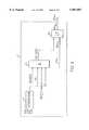
- FIG. 3illustrates a manner of the invention of setting the EFCI bit in the UTOPIA interface.
- the EFCI bitis manipulated in a circuit 31, into which out of the UTOPIA interface signals a clock signal CLK, a Start of Cell signal SOC, an ENABLE signal ENB* and signals of data conductors D3 and D4 are led.
- an ENB signal *indicates that data transmission is in process.
- An EFCI -- Threshold signalthe only signal from outside the UTOPIA interface, is also led to the manipulation circuit. This signal indicates whether the EFCI bit is to be set (in user cells) to value "1", indicating that congestion has been detected. Information on congestion can be received from e.g. an ATM device buffer 32 when its fill rate has exceeded a given predetermined limit.
- a SOC signal received by the manipulation circuit 31indicates when data from the UTOPIA interface comprises the first byte (denoted in the Figure by reference numeral 1) of the cell.
- the data conductori.e. D3 corresponding to the bit to be manipulated (EFCI) is led to the manipulation circuit 31 and the other data conductors (D1, D2 and D4 to D8) are led directly past the manipulation circuit.
- the signal of the data conductor D4is led to the manipulation circuit in order for the manipulation circuit to receive information on when a user cell is concerned (cf. the above table). This signal is denoted by reference UC.
- the bit to be manipulatedis searched for in circuit 31 by counting from start of cell up to the byte comprising the bit to be manipulated. Counting is allowed only when the ENB* signal is active. When the counter has reached the desired value, the bit is manipulated.
- An output conductor D3 out corresponding to the manipulated bitis led from the manipulation circuit to its own position among the conductors that bypassed the circuit, the byte-wide data being again assembled, the EFCI bit, however, having its manipulated value. Even though several signals are led to the manipulations circuit, the signal corresponding to the header bit to be manipulated is the only one to pass through the manipulation circuit (i.e. the circuit has only one output).
- FIG. 4illustrates the function of a manipulation circuit.
- the circuithas two modes: idle mode A1 and counting mode A2.
- idle modethe circuit waits until it gets information on the start of a cell. This occurring, (signal SOC becoming active) the circuit switches to counting mode A2 and starts the internal counter (shown in FIG. 5 with reference numeral 50) of the circuit.
- the countercounts, synchronized by the clock signal, up to the desired header bit (fourth bit in an EFCI byte).
- the desired header bitfourth bit in an EFCI byte.
- the output signal of the circuit 31has the same value as its input signal, i.e. the value of the bit concerned is in no way affected.
- FIG. 5shows an example of implementing combination logic and FIG. 6 shows a corresponding timing diagram.
- the output signal CV'(in a logical state "1" when counter value is four, i.e. the fourth byte of a cell is concerned) of the above counter 50, an inverted signal UC (having the value one when a user cell is concerned) of the signal conductor D4, and the EF-Cl -- Threshold signal (having the value one when congestion has been detected) are led to an AND gate 51.
- a SET -- EFCI output signalin a logical one state when all input signals have simultaneously the value one) of the AND gate is connected to the first input of an OR gate 52.
- An EFCI in signal received from an input conductor D3 inis coupled to another input of the OR gate. That is, the OR gate converts an incoming signal (an EFCI bit) with the value "zero” to an output signal with the value "one” when all signals incoming to the AND gate are in a state one.
- a fourth input signal ENABLE for indicating when the manipulation of the invention is effectivecan be added to the AND gate (e.g. to control the manipulation).
- bit manipulation in microcircuitsonly takes a fraction of the cycle of the byte clock available.
- bit manipulation in microcircuitsonly takes a fraction of the cycle of the byte clock available.
- the bithas had time to change long before decisions on the byte concerned are made at the next interface.
- byte datais sufficiently stable in a decision-making process (which usually takes place on the rising edge of the clock).
- the ENB* signalmanages flow control so that when transmission is disconnected, the state of the ENB* signal changes (cf. FIG. 6). If the intention is to implement a modified UTOPIA interface without the above byte-based flow control and with e.g. only cell-based flow control which can be managed with the SOC signal, the ENB* signal can be totally omitted.
- FIGS. 7 and 8Such an alternative is shown in FIGS. 7 and 8 in which a modified manipulation circuit is denoted by reference numeral 31'. As can be seen from FIGS. 5 and 8, the modified manipulation circuit corresponds to the above except that the ENB* signal is not used at all.
Landscapes
- Engineering & Computer Science (AREA)
- Computer Networks & Wireless Communication (AREA)
- Signal Processing (AREA)
- Data Exchanges In Wide-Area Networks (AREA)
Abstract
Description
______________________________________ PTI coding Interpretation ______________________________________Bits 4 3 2 0 0 0 User cell, no congestion (I=0). 0 0 1 User cell, no congestion (I=1). 0 1 0 User cell, congestion (I=0). 0 1 1 User cell, congestion (I=1). 1 0 0OAM cell 1 0 1OAM cell 1 1 0RM cell 1 1 1 Reserved ______________________________________
Claims (6)
Applications Claiming Priority (2)
| Application Number | Priority Date | Filing Date | Title |
|---|---|---|---|
| FI960665 | 1996-02-14 | ||
| FI960665AFI103545B (en) | 1996-02-14 | 1996-02-14 | Manipulation of the ATM cell header field |
Publications (1)
| Publication Number | Publication Date |
|---|---|
| US5987007Atrue US5987007A (en) | 1999-11-16 |
Family
ID=8545451
Family Applications (1)
| Application Number | Title | Priority Date | Filing Date |
|---|---|---|---|
| US08/800,326Expired - LifetimeUS5987007A (en) | 1996-02-14 | 1997-02-14 | Manipulation of header field in ATM cell |
Country Status (3)
| Country | Link |
|---|---|
| US (1) | US5987007A (en) |
| EP (1) | EP0794685A1 (en) |
| FI (1) | FI103545B (en) |
Cited By (7)
| Publication number | Priority date | Publication date | Assignee | Title |
|---|---|---|---|---|
| US20010047893A1 (en)* | 2000-05-31 | 2001-12-06 | Shimadzu Corporation | Electronic balance |
| US20020031132A1 (en)* | 2000-05-25 | 2002-03-14 | Mcwilliams Patrick | UTOPIA-LVDS bridge |
| US20020031141A1 (en)* | 2000-05-25 | 2002-03-14 | Mcwilliams Patrick | Method of detecting back pressure in a communication system using an utopia-LVDS bridge |
| US20020031133A1 (en)* | 2000-05-25 | 2002-03-14 | Mcwilliams Patrick | Embedded communication protocol using a UTOPIA-LVDS bridge |
| US6618383B1 (en)* | 1999-12-28 | 2003-09-09 | Nortel Networks Limited | Serial interface for a broadband communications network |
| US20040246966A1 (en)* | 2003-06-05 | 2004-12-09 | Globespan Virata Incorporated | ATM header compression using hash tables |
| US20100101807A1 (en)* | 2008-10-27 | 2010-04-29 | Donald Roy Greenlee | Downhole apparatus with packer cup and slip |
Citations (11)
| Publication number | Priority date | Publication date | Assignee | Title |
|---|---|---|---|---|
| US4947388A (en)* | 1988-04-06 | 1990-08-07 | Hitachi, Ltd. | Cell switching system of asynchronous transfer mode |
| EP0498408A1 (en)* | 1991-02-05 | 1992-08-12 | Fujitsu Limited | ATM exchange system with management cells |
| US5193088A (en)* | 1990-06-27 | 1993-03-09 | Electronics And Telecommunications Research Institute | High speed ATM cell synchronizing switching apparatus |
| WO1995001029A1 (en)* | 1993-06-21 | 1995-01-05 | Gpt Limited | Flow control method |
| EP0647081A2 (en)* | 1993-09-06 | 1995-04-05 | Kabushiki Kaisha Toshiba | Method and apparatus for controlling congestion in a communication network |
| EP0661851A2 (en)* | 1993-12-22 | 1995-07-05 | Nec Corporation | Congestion control method in ATM network |
| US5488606A (en)* | 1993-09-20 | 1996-01-30 | Fujitsu Limited | Procedure for switching-over systems |
| US5515359A (en)* | 1994-08-26 | 1996-05-07 | Mitsubishi Electric Research Laboratories, Inc. | Credit enhanced proportional rate control system |
| US5696764A (en)* | 1993-07-21 | 1997-12-09 | Fujitsu Limited | ATM exchange for monitoring congestion and allocating and transmitting bandwidth-guaranteed and non-bandwidth-guaranteed connection calls |
| US5768273A (en)* | 1995-04-05 | 1998-06-16 | International Business Machines Corporation | Method and apparatus for priority level queueing in processing ATM cell header and payload |
| US5815737A (en)* | 1995-06-05 | 1998-09-29 | Pmc-Sierra, Inc. | Approach for identifying a subset of asynchronous transfer mode (ATM) VPI/VCI values in the complete VPI/VCI range |
- 1996
- 1996-02-14FIFI960665Apatent/FI103545B/enactive
- 1997
- 1997-02-11EPEP97660012Apatent/EP0794685A1/ennot_activeWithdrawn
- 1997-02-14USUS08/800,326patent/US5987007A/ennot_activeExpired - Lifetime
Patent Citations (11)
| Publication number | Priority date | Publication date | Assignee | Title |
|---|---|---|---|---|
| US4947388A (en)* | 1988-04-06 | 1990-08-07 | Hitachi, Ltd. | Cell switching system of asynchronous transfer mode |
| US5193088A (en)* | 1990-06-27 | 1993-03-09 | Electronics And Telecommunications Research Institute | High speed ATM cell synchronizing switching apparatus |
| EP0498408A1 (en)* | 1991-02-05 | 1992-08-12 | Fujitsu Limited | ATM exchange system with management cells |
| WO1995001029A1 (en)* | 1993-06-21 | 1995-01-05 | Gpt Limited | Flow control method |
| US5696764A (en)* | 1993-07-21 | 1997-12-09 | Fujitsu Limited | ATM exchange for monitoring congestion and allocating and transmitting bandwidth-guaranteed and non-bandwidth-guaranteed connection calls |
| EP0647081A2 (en)* | 1993-09-06 | 1995-04-05 | Kabushiki Kaisha Toshiba | Method and apparatus for controlling congestion in a communication network |
| US5488606A (en)* | 1993-09-20 | 1996-01-30 | Fujitsu Limited | Procedure for switching-over systems |
| EP0661851A2 (en)* | 1993-12-22 | 1995-07-05 | Nec Corporation | Congestion control method in ATM network |
| US5515359A (en)* | 1994-08-26 | 1996-05-07 | Mitsubishi Electric Research Laboratories, Inc. | Credit enhanced proportional rate control system |
| US5768273A (en)* | 1995-04-05 | 1998-06-16 | International Business Machines Corporation | Method and apparatus for priority level queueing in processing ATM cell header and payload |
| US5815737A (en)* | 1995-06-05 | 1998-09-29 | Pmc-Sierra, Inc. | Approach for identifying a subset of asynchronous transfer mode (ATM) VPI/VCI values in the complete VPI/VCI range |
Cited By (10)
| Publication number | Priority date | Publication date | Assignee | Title |
|---|---|---|---|---|
| US6618383B1 (en)* | 1999-12-28 | 2003-09-09 | Nortel Networks Limited | Serial interface for a broadband communications network |
| US20020031132A1 (en)* | 2000-05-25 | 2002-03-14 | Mcwilliams Patrick | UTOPIA-LVDS bridge |
| US20020031141A1 (en)* | 2000-05-25 | 2002-03-14 | Mcwilliams Patrick | Method of detecting back pressure in a communication system using an utopia-LVDS bridge |
| US20020031133A1 (en)* | 2000-05-25 | 2002-03-14 | Mcwilliams Patrick | Embedded communication protocol using a UTOPIA-LVDS bridge |
| US20010047893A1 (en)* | 2000-05-31 | 2001-12-06 | Shimadzu Corporation | Electronic balance |
| US20040246966A1 (en)* | 2003-06-05 | 2004-12-09 | Globespan Virata Incorporated | ATM header compression using hash tables |
| US20080151903A1 (en)* | 2003-06-05 | 2008-06-26 | Conexant Systems, Inc. | ATM Header Compression Using Hash Tables |
| US7400627B2 (en) | 2003-06-05 | 2008-07-15 | Brooktree Broadband Holding, Inc. | ATM header compression using hash tables |
| US7720071B2 (en) | 2003-06-05 | 2010-05-18 | Ikanos Communications, Inc. | ATM header compression using hash tables |
| US20100101807A1 (en)* | 2008-10-27 | 2010-04-29 | Donald Roy Greenlee | Downhole apparatus with packer cup and slip |
Also Published As
| Publication number | Publication date |
|---|---|
| FI103545B1 (en) | 1999-07-15 |
| FI960665A7 (en) | 1997-08-15 |
| FI960665A0 (en) | 1996-02-14 |
| FI103545B (en) | 1999-07-15 |
| EP0794685A1 (en) | 1997-09-10 |
Similar Documents
| Publication | Publication Date | Title |
|---|---|---|
| US6243382B1 (en) | Interfacing to SAR devices in ATM switching apparatus | |
| EP0993157B1 (en) | Memory-efficient leaky bucket policer for traffic management of asynchronous transfer mode data communications | |
| US6349098B1 (en) | Method and apparatus for forming a virtual circuit | |
| US5889778A (en) | ATM layer device | |
| US5379295A (en) | Cross-connect system for asynchronous transfer mode | |
| US6032272A (en) | Method and apparatus for performing packet based policing | |
| US7830893B2 (en) | Real time segmentation and reassembly of asynchronous transfer mode (ATM) adaptation layer two (AAL2) and AAL5 data | |
| US7050442B1 (en) | Communications system, bus and method for communication of ATM data traffic | |
| JP2000059370A (en) | Traffic control apparatus and method | |
| US5987007A (en) | Manipulation of header field in ATM cell | |
| US6628659B1 (en) | ATM cell switching system | |
| US6430197B1 (en) | Asynchronous transfer mode (ATM) cell multiplexing/demultiplexing apparatus | |
| Cisco | ATM Technology | |
| Cisco | ATM Technology | |
| Cisco | ATM Technology | |
| Cisco | ATM Technology | |
| Cisco | ATM Technology | |
| Cisco | ATM Technology | |
| Cisco | ATM Technology | |
| Cisco | ATM Technology | |
| Cisco | ATM Technology | |
| Cisco | ATM Technology | |
| Cisco | ATM Technology | |
| Cisco | ATM Technology | |
| Cisco | ATM Technology |
Legal Events
| Date | Code | Title | Description |
|---|---|---|---|
| AS | Assignment | Owner name:NOKIA TELECOMMUNICATIONS OY, FINLAND Free format text:ASSIGNMENT OF ASSIGNORS INTEREST;ASSIGNORS:MOLIN, KIM;HAVANTO, PETRI;KAAJA, HARALD;AND OTHERS;REEL/FRAME:008752/0128;SIGNING DATES FROM 19970122 TO 19970207 | |
| AS | Assignment | Owner name:NOKIA TELECOMMUNICATIONS OY, FINLAND Free format text:CORRECTIV;ASSIGNORS:MOLIN, KIM;HAVANTO, PETRI;KAAJA, HARALD;AND OTHERS;REEL/FRAME:008854/0830;SIGNING DATES FROM 19970129 TO 19970207 | |
| STCF | Information on status: patent grant | Free format text:PATENTED CASE | |
| FPAY | Fee payment | Year of fee payment:4 | |
| FEPP | Fee payment procedure | Free format text:PAYOR NUMBER ASSIGNED (ORIGINAL EVENT CODE: ASPN); ENTITY STATUS OF PATENT OWNER: LARGE ENTITY Free format text:PAYER NUMBER DE-ASSIGNED (ORIGINAL EVENT CODE: RMPN); ENTITY STATUS OF PATENT OWNER: LARGE ENTITY | |
| FPAY | Fee payment | Year of fee payment:8 | |
| AS | Assignment | Owner name:NOKIA CORPORATION, FINLAND Free format text:MERGER;ASSIGNOR:NOKIA TELECOMMUNICATIONS OY;REEL/FRAME:021400/0205 Effective date:20010130 Owner name:SPYDER NAVIGATIONS L.L.C., DELAWARE Free format text:ASSIGNMENT OF ASSIGNORS INTEREST;ASSIGNOR:NOKIA CORPORATION;REEL/FRAME:021401/0725 Effective date:20070322 | |
| FEPP | Fee payment procedure | Free format text:PAYOR NUMBER ASSIGNED (ORIGINAL EVENT CODE: ASPN); ENTITY STATUS OF PATENT OWNER: LARGE ENTITY Free format text:PAYER NUMBER DE-ASSIGNED (ORIGINAL EVENT CODE: RMPN); ENTITY STATUS OF PATENT OWNER: LARGE ENTITY | |
| FPAY | Fee payment | Year of fee payment:12 | |
| AS | Assignment | Owner name:INTELLECTUAL VENTURES I LLC, DELAWARE Free format text:MERGER;ASSIGNOR:SPYDER NAVIGATIONS L.L.C.;REEL/FRAME:026637/0611 Effective date:20110718 | |
| AS | Assignment | Owner name:HANGER SOLUTIONS, LLC, GEORGIA Free format text:ASSIGNMENT OF ASSIGNORS INTEREST;ASSIGNOR:INTELLECTUAL VENTURES ASSETS 161 LLC;REEL/FRAME:052159/0509 Effective date:20191206 | |
| AS | Assignment | Owner name:INTELLECTUAL VENTURES ASSETS 161 LLC, DELAWARE Free format text:ASSIGNMENT OF ASSIGNORS INTEREST;ASSIGNOR:INTELLECTUAL VENTURES I LLC;REEL/FRAME:051945/0001 Effective date:20191126 |