US5986899A - Single ended forward DC-to-DC converter providing enhanced resetting for synchronous rectification - Google Patents
Single ended forward DC-to-DC converter providing enhanced resetting for synchronous rectificationDownload PDFInfo
- Publication number
- US5986899A US5986899AUS09/266,199US26619999AUS5986899AUS 5986899 AUS5986899 AUS 5986899AUS 26619999 AUS26619999 AUS 26619999AUS 5986899 AUS5986899 AUS 5986899A
- Authority
- US
- United States
- Prior art keywords
- primary
- voltage
- switch
- transformer
- secondary winding
- Prior art date
- Legal status (The legal status is an assumption and is not a legal conclusion. Google has not performed a legal analysis and makes no representation as to the accuracy of the status listed.)
- Expired - Lifetime
Links
- 230000001360synchronised effectEffects0.000titleabstractdescription11
- 239000003990capacitorSubstances0.000claimsabstractdescription38
- 238000004891communicationMethods0.000claimsdescription8
- 238000004804windingMethods0.000abstractdescription109
- 230000008859changeEffects0.000abstractdescription3
- 230000005415magnetizationEffects0.000abstractdescription3
- 238000000034methodMethods0.000description5
- 238000009499grossingMethods0.000description4
- 230000001939inductive effectEffects0.000description3
- 230000004907fluxEffects0.000description2
- 230000004044responseEffects0.000description2
- 230000003213activating effectEffects0.000description1
- 238000006243chemical reactionMethods0.000description1
- 230000009849deactivationEffects0.000description1
- 230000007423decreaseEffects0.000description1
- 230000001419dependent effectEffects0.000description1
- 238000010586diagramMethods0.000description1
- 230000000694effectsEffects0.000description1
- 230000002708enhancing effectEffects0.000description1
- 230000001747exhibiting effectEffects0.000description1
- 238000012986modificationMethods0.000description1
- 230000004048modificationEffects0.000description1
- 230000000737periodic effectEffects0.000description1
Images


Classifications
- H—ELECTRICITY
- H02—GENERATION; CONVERSION OR DISTRIBUTION OF ELECTRIC POWER
- H02M—APPARATUS FOR CONVERSION BETWEEN AC AND AC, BETWEEN AC AND DC, OR BETWEEN DC AND DC, AND FOR USE WITH MAINS OR SIMILAR POWER SUPPLY SYSTEMS; CONVERSION OF DC OR AC INPUT POWER INTO SURGE OUTPUT POWER; CONTROL OR REGULATION THEREOF
- H02M3/00—Conversion of DC power input into DC power output
- H02M3/22—Conversion of DC power input into DC power output with intermediate conversion into AC
- H02M3/24—Conversion of DC power input into DC power output with intermediate conversion into AC by static converters
- H02M3/28—Conversion of DC power input into DC power output with intermediate conversion into AC by static converters using discharge tubes with control electrode or semiconductor devices with control electrode to produce the intermediate AC
- H02M3/325—Conversion of DC power input into DC power output with intermediate conversion into AC by static converters using discharge tubes with control electrode or semiconductor devices with control electrode to produce the intermediate AC using devices of a triode or a transistor type requiring continuous application of a control signal
- H02M3/335—Conversion of DC power input into DC power output with intermediate conversion into AC by static converters using discharge tubes with control electrode or semiconductor devices with control electrode to produce the intermediate AC using devices of a triode or a transistor type requiring continuous application of a control signal using semiconductor devices only
- H02M3/33569—Conversion of DC power input into DC power output with intermediate conversion into AC by static converters using discharge tubes with control electrode or semiconductor devices with control electrode to produce the intermediate AC using devices of a triode or a transistor type requiring continuous application of a control signal using semiconductor devices only having several active switching elements
- H02M3/33576—Conversion of DC power input into DC power output with intermediate conversion into AC by static converters using discharge tubes with control electrode or semiconductor devices with control electrode to produce the intermediate AC using devices of a triode or a transistor type requiring continuous application of a control signal using semiconductor devices only having several active switching elements having at least one active switching element at the secondary side of an isolation transformer
- H—ELECTRICITY
- H02—GENERATION; CONVERSION OR DISTRIBUTION OF ELECTRIC POWER
- H02M—APPARATUS FOR CONVERSION BETWEEN AC AND AC, BETWEEN AC AND DC, OR BETWEEN DC AND DC, AND FOR USE WITH MAINS OR SIMILAR POWER SUPPLY SYSTEMS; CONVERSION OF DC OR AC INPUT POWER INTO SURGE OUTPUT POWER; CONTROL OR REGULATION THEREOF
- H02M3/00—Conversion of DC power input into DC power output
- H02M3/22—Conversion of DC power input into DC power output with intermediate conversion into AC
- H02M3/24—Conversion of DC power input into DC power output with intermediate conversion into AC by static converters
- H02M3/28—Conversion of DC power input into DC power output with intermediate conversion into AC by static converters using discharge tubes with control electrode or semiconductor devices with control electrode to produce the intermediate AC
- H02M3/325—Conversion of DC power input into DC power output with intermediate conversion into AC by static converters using discharge tubes with control electrode or semiconductor devices with control electrode to produce the intermediate AC using devices of a triode or a transistor type requiring continuous application of a control signal
- H02M3/335—Conversion of DC power input into DC power output with intermediate conversion into AC by static converters using discharge tubes with control electrode or semiconductor devices with control electrode to produce the intermediate AC using devices of a triode or a transistor type requiring continuous application of a control signal using semiconductor devices only
- H02M3/33569—Conversion of DC power input into DC power output with intermediate conversion into AC by static converters using discharge tubes with control electrode or semiconductor devices with control electrode to produce the intermediate AC using devices of a triode or a transistor type requiring continuous application of a control signal using semiconductor devices only having several active switching elements
- H02M3/33576—Conversion of DC power input into DC power output with intermediate conversion into AC by static converters using discharge tubes with control electrode or semiconductor devices with control electrode to produce the intermediate AC using devices of a triode or a transistor type requiring continuous application of a control signal using semiconductor devices only having several active switching elements having at least one active switching element at the secondary side of an isolation transformer
- H02M3/33592—Conversion of DC power input into DC power output with intermediate conversion into AC by static converters using discharge tubes with control electrode or semiconductor devices with control electrode to produce the intermediate AC using devices of a triode or a transistor type requiring continuous application of a control signal using semiconductor devices only having several active switching elements having at least one active switching element at the secondary side of an isolation transformer having a synchronous rectifier circuit or a synchronous freewheeling circuit at the secondary side of an isolation transformer
- Y—GENERAL TAGGING OF NEW TECHNOLOGICAL DEVELOPMENTS; GENERAL TAGGING OF CROSS-SECTIONAL TECHNOLOGIES SPANNING OVER SEVERAL SECTIONS OF THE IPC; TECHNICAL SUBJECTS COVERED BY FORMER USPC CROSS-REFERENCE ART COLLECTIONS [XRACs] AND DIGESTS
- Y02—TECHNOLOGIES OR APPLICATIONS FOR MITIGATION OR ADAPTATION AGAINST CLIMATE CHANGE
- Y02B—CLIMATE CHANGE MITIGATION TECHNOLOGIES RELATED TO BUILDINGS, e.g. HOUSING, HOUSE APPLIANCES OR RELATED END-USER APPLICATIONS
- Y02B70/00—Technologies for an efficient end-user side electric power management and consumption
- Y02B70/10—Technologies improving the efficiency by using switched-mode power supplies [SMPS], i.e. efficient power electronics conversion e.g. power factor correction or reduction of losses in power supplies or efficient standby modes
Definitions
- This inventionrelates to DC-to-DC converters, more particularly to single ended forward DC-to-DC converters having circuitry for resetting a transformer core.
- DC-to-DC convertersare used to convert an input DC voltage to a different output DC voltage for delivery to a load.
- Such converterstypically comprise a transformer that is electrically coupled via a switching circuit between the voltage source and the load.
- Converters known as single-ended forward convertersare a class of converters that rely on a single switch connected between the voltage source and the primary winding of the transformer to provide forward power transfer to the secondary winding of the transformer when the switch is on and conducting.
- the transformer coreis "reset” during the off period of the switch. Resetting is typically accomplished with the use of additional circuitry, such as a third transformer winding in parallel with the primary transformer winding, or a LC resonant circuit electrically coupled to the secondary winding.
- additional circuitrysuch as a third transformer winding in parallel with the primary transformer winding, or a LC resonant circuit electrically coupled to the secondary winding.
- the driving waveforms of such circuitryexhibit a "dead time", a period during which the switch remains open, the voltage across the switch equals the source voltage, and the current vanishes. Dead time decreases the overall efficiency of the converter and places voltage stresses on the switch.
- the inventionrelates to a single ended forward DC-to-DC converter that effectively resets the transformer core, thereby enhancing its ability to carry out self-driven synchronous rectification.
- the convertercomprises a transformer having a primary winding electrically connected to a primary switch, and a secondary winding electrically connected to a secondary switch and a clamping capacitor.
- the secondary windingis in electrical communication with a pair of rectifiers and an LC filter circuit that provides rectification and smoothing of the power signal that reaches the load.
- the primary switchis on, the primary winding is conductive and an input voltage exists across the secondary winding.
- the secondary switchWhen the primary switch is turned off, the secondary switch is turned on, a magnetizing current existing in the secondary winding is transferred to the clamping capacitor, and the clamping capacitor is charged to substantially the input voltage. During the period that the primary switch is off, the voltage across the secondary winding is maintained constant, and the transformer core is reset
- the primary and secondary switchesinclude MOSFET switches.
- the primary MOSFET switchwhen the primary MOSFET switch is open, a voltage appearing at the secondary winding causes the secondary MOSFET switch to become conductive.
- the primary switchcomprises an n-channel MOSFET and the secondary switch comprises a p-channel MOSFET.
- the secondary switchcomprises an n-channel MOSFET and the secondary winding is electrically coupled with a third winding. The third winding provides a positive voltage necessary to activate the n-channel MOSFET.
- inventionsrelate to a method for resetting the core of the transformer by activating and deactivating a primary MOSFET coupled to a primary winding of a transformer, such that upon deactivation, the secondary MOSFET is activated, a clamping capacitor is charged, and the secondary winding is clamped to the voltage of a clamping capacitor.
- the present inventionprovides synchronous rectification and zero voltage switching, techniques that are useful in providing lower output voltages and higher power densities at the load. Moreover, the use of a clamping capacitor and MOSFET switches increases the simplicity of the DC-to-DC converter while eliminating undesirable characteristics such as dead time and voltage stresses on the switches.
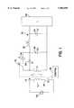
- FIG. 1is a single-ended forward DC-to-DC converter according to one embodiment of the invention.
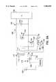
- FIG. 2Ais a single-ended forward DC-to-DC converter according to another embodiment of the invention.
- FIG. 2Bis a section of the single-ended forward DC-to-DC converter of FIG. 2A that is conducting when the primary switch is on.
- FIG. 2Cis a section of the single-ended forward DC-to-DC converter of FIG. 2A that is conducting when the primary switch is off.
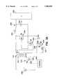
- FIG. 3Ais a single-ended forward DC-to-DC converter according to yet another embodiment of the invention.
- FIG. 3Bis a section of the single-ended forward DC-to-DC converter of FIG. 3A that is conducting when the primary switch is on.
- FIG. 3Cis a section of the single-ended forward DC-to-DC converter of FIG. 3A that is conducting when the primary switch is off.
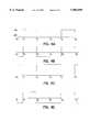
- FIG. 4Ais a waveform showing the periods during which the primary switch of the single-ended forward DC-to-DC converter is on and off.
- FIG. 4Bis a waveform showing the voltage across the primary winding of the transformer of the single-ended forward DC-to-DC converter during the periods when the primary switch is on and off.
- FIG. 4Cis a waveform showing the voltage across the primary switch of the single-ended forward DC-to-DC converter during the periods when the primary switch is on and off.
- FIG. 4Dis a waveform showing the voltage across the secondary winding of the transformer of the single-ended forward DC-to-DC converter during the periods when the primary switch is on and off.
- FIG. 1An embodiment of the single ended forward DC-to-DC converter is shown in FIG. 1.
- a transformer 10is electrically coupled between a DC power source 20, having a certain input voltage V, and a load 50.
- the transformer 10includes a primary winding 12 and a secondary winding 14.
- the number of turns of the windingsdepends upon the desired output voltage at the load 50.
- the input voltageis typically 48 V and the desired output voltage is typically 4 V, thus requiring a turns ratio of about 12:1.
- the transformer 10will be considered as having a turns ratio of 1:1.
- a primary switch 16Electrically connected in series between the primary winding 12 and the source 20 is a primary switch 16, designated as Q1.
- Q1When the switch 16 is on, that is, when the switch 16 is in the closed state, a closed circuit is formed, and current flows from the source 20 through the primary winding 12 and back to the source 20, inducing a voltage in the secondary winding 14.
- a secondary switch 22Electrically connected in series with the secondary winding 14 is a secondary switch 22, designated as Q2, and a clamping capacitor 24. As will be further described below, the clamping capacitor 24 charges when the secondary switch 22 is on.
- a diode 26, designated by D1is electrically connected in series with the secondary winding 14 of the transformer 10, and is electrically connected in parallel with the secondary switch 22 and the clamping capacitor 24. As will be further described below, the diode 26 is conductive when the primary switch 16 is on.
- a second diode 28, designated by D2is electrically connected in parallel with the secondary winding 14 of the transformer 10. In electrical communication with the secondary winding 14 and the diode 26, is an LC circuit 30.
- the LC circuit 30includes a filter inductor 32 in series with the secondary winding 14 and the diode 28, and a filter capacitor 34 in parallel with the secondary winding 14 and the diode 28.
- the diodes 26, 28 and the LC circuit 30, in combination,provide a rectifying and smoothing circuit, that filters the voltage from the secondary winding before it reaches the load 50.
- a control device 40is electrically coupled to the primary switch 16 and the secondary switch 22.
- the control device 40controls the operation of the primary switch 16 and the secondary switch 22, causing them to turn on and off at desired times.
- the control device 40preferably activates the switches 16, 22 out of phase, and in the present embodiment, the control device 40 can introduce a small period of delay, during which both switches 16, 22 are in an off-state.
- Such a period of delaycan be configured such that the secondary switch 22 turns on after a predetermined period of time has elapsed after the primary switch 16 has turned off. This delay allows zero voltage switching to be accomplished, as the voltage at the primary switch 16 is returned to about zero volts before the primary switch 16 is again turned on.
- a magnetizing current present in the transformer 10 after the primary switch 16 is turned offis used to maintain a constant voltage across the secondary winding.
- control device 40When the control device 40 causes the primary switch 16 to turn on, current flows through the primary winding 12, inducing a current in the secondary winding 14, which flows through the diode 26 to the LC circuit 30.
- the LC circuit 30smoothes the voltage appearing across the secondary winding 14, and a DC output is obtained at the load 50.
- the control device 40causes the primary switch 16 to turn off, the forward transfer of current through the primary winding 12 and the secondary winding 14 terminates.
- the diode 28then becomes conductive, allowing the energy stored in the field of the filter inductor 32 to be released into the filter capacitor 34 and the load 50.
- magnetizing current in the transformeris stored in the clamping capacitor 24, which in turn, clamps the voltage at the secondary winding 14 of the transformer 10 to substantially the magnitude of the input voltage.
- the voltage at the secondary winding 14thus remains substantially constant and the transformer 10 is reset, as the direction of the magnetic flux in the transformer is reversed.
- the capacitance of the clamping capacitor 34is sufficiently large such that the time dependence of the voltage across the clamping capacitor 34 is negligible.
- the volt-second product impressed on the secondary winding 14 of the transformer 10 during the time period that the primary switch 16 is onis equal to the volt-second product impressed on the secondary winding 14 when the primary switch 16 is off. This can be expressed mathematically for a transformer 10 having a turns ratio of 1:1, as:
- t onis the period during which the primary switch 16 is on
- t offis the period during which the primary switch 16 is off.
- a transformer 110is electrically coupled between a DC power source 120 having a certain input voltage V, and a load 150.
- the transformer 110includes a primary winding 112 and a secondary winding 114. Electrically connected in series with the primary winding 112 is a primary switch 116, a n-channel MOSFET designated by Q3.
- the primary winding 112is electrically connected to the drain terminal 118 of the MOSFET 116 and a DC source 120 is electrically connected to the source terminal 122 of the MOSFET 116.
- a control device 140is electrically connected to the gate terminal 124 of the MOSFET 116, and applies a voltage at the gate 124, selectively causing the MOSFET 116 to turn on.
- the MOSFET 116When the MOSFET 116 is on, it forms a closed circuit with the primary winding 112 and the voltage source 120.
- the DC source 120can be electrically connected to the drain terminal 118
- the primary winding 112can be electrically connected to the source terminal 122, provided that the polarity of the input at the drain terminal 118 of the MOSFET 116 results in the MOSFET 116 becoming forward and reversed biased in response to an input from the control device 140 at the gate terminal 124.
- a rectifier 126a n-channel MOSFET designated as D3, is electrically connected in series with the secondary winding 114 of the transformer 10. As will be further described, the rectifier 126 is conductive when the MOSFET 116 is on. The rectifier 126 is in parallel with the secondary switch 130 and a clamping capacitor 132.
- the secondary switch 130is a p-channel MOSFET, designated by Q4.
- the drain terminal 136 and the gate terminal 138 of the p-channel MOSFET 130are connected across the secondary winding 114 such that the MOSFET 130 becomes forward biased in response to a change in the voltage across the secondary winding 114.
- the source terminal 139is connected to the clamping capacitor 132.
- a second rectifier 134a n-channel MOSFET designated by D4, is electrically connected in series with the clamping capacitor 132, and in parallel with the secondary winding 114 of the transformer 110.
- a LC circuit 160In electrical communication with the secondary winding 114 and the rectifier 134, is a LC circuit 160.
- the LC circuit 160includes a filter inductor 162 in series with the secondary winding 114 and the rectifier 134, and a filter capacitor 164 in parallel with the secondary winding 114 and the rectifier 134.
- the rectifiers 126 and 134function to provide self-driven synchronous rectification.
- the rectifiers 126, 134reduce the input voltage such that the voltage appearing across the LC circuit is lower.
- the combination of the rectifiers 126 and 134, and the LC circuit 160provide a rectifying and smoothing circuit.
- FIG. 2Bshown is a section of the circuitry of the converter of FIG. 2A that is conductive when the control device 140 causes the primary switch 116, n-channel MOSFET Q3, to turn on.
- the MOSFET 116When the MOSFET 116 is conducting, a closed circuit is thus formed, as an input voltage exists across the primary winding 112 causing current to flow from the voltage source 120, through the primary winding 112 of the transformer 110, and induce a voltage in the secondary winding 114.
- the voltage across the secondary winding 114causes the rectifier 126 to be forward biased, and current flows through the LC circuit 160.
- the LC circuit 160smoothes the voltage appearing across the secondary winding 114, and a DC output is obtained at the load 150.
- FIG. 2Cshown is a section of the circuitry of the converter of FIG. 2A that is conductive when the control device 140 causes n-channel MOSFET 116 to turn off Note that a dashed-line connection is shown between the DC source 120 and the primary winding 112 and MOSFET 116, to indicate that no current is flowing through the MOSFET 116 or the primary winding 112.
- the n-channel MOSFET 116is reversed biased, the forward transfer of current through the primary winding 112 to the secondary winding 114 terminates.
- the voltage across the secondary winding 114causes the rectifier 134, n-channel MOSFET D4, to become forward biased, allowing the energy stored in the filter inductor 162 to release current into the filter capacitor 164 and the load 150.
- the voltage across the secondary winding 114causes the secondary switch 130, p-channel MOSFET Q4, to become conductive.
- the magnetizing current in the secondary winding 114thus flows from the drain 136 to the source 139, causing the clamping capacitor 132 to charge.
- the clamping capacitor 132thus clamps the voltage at the secondary winding 114 of the transformer 110 to substantially the input voltage V, during the time period that the n-channel MOSFET 116 is off. It is important to note that the self-driving characteristics of the secondary switch 130 obtained with the MOSFET Q4, eliminates the need for the control device 140 to be connected to the MOSFET 130 to turn it on and off.
- a transformer 210is electrically connected between a DC power source 220 having a certain input voltage, and a load 250.
- the transformer 210includes a primary winding 212 and a secondary winding 214. Electrically connected in series with the primary winding 212 is a primary switch 216, a n-channel MOSFET designated by Q5.
- the primary winding 212is electrically connected between the drain terminal 218 of the MOSFET 216 and the DC source 220, and the DC source 220 is also electrically connected to the source terminal 222 of the MOSFET 216.
- MOSFET 216 terminal connectionsmay differ for the primary winding 212 and the voltage source 220, provided that the operation of the MOSFET 216 remains the same.
- a control device 240is electrically connected to the gate terminal 224 of the MOSFET 216, and applies a voltage at the gate 224, selectively causing the MOSFET 216 to become conductive. When the MOSFET 216 is conducting, it forms a closed circuit with the primary winding 112 and the voltage source 120.
- a secondary switch 230Electrically connected in series with the secondary winding 214 is a secondary switch 230, n-channel MOSFET designated by Q6, which is conductive when the primary switch 216, n-channel MOSFET Q5, is off.
- the gate terminal 238 of the n-channel MOSFET 230is electrically connected to a third winding 237 of the transformer, which is in parallel with the output of the drain terminal 236.
- the third winding 237provides the positive voltage necessary to turn on the secondary switch 230.
- the source terminal 239 of the MOSFET 230is electrically connected to a clamping capacitor 232.
- a rectifier 226, n-channel MOSFET designated as D5is also electrically connected in series with the secondary winding 214 of the transformer 210.
- the rectifier 226is conductive when the MOSFET 216, is conductive.
- the rectifier 226is also in parallel with the secondary switch 230, MOSFET Q6, and the clamping capacitor 232.
- a second rectifier 234, a n-channel MOSFET designated by D6,is electrically connected in series with the clamping capacitor 232, and in parallel with the secondary winding 214 of the transformer 210.
- the LC circuit 260comprises a filter inductor 262 in series with the secondary winding 214 and the rectifier 234, and a filter capacitor 264 in parallel with the secondary winding 214 and the rectifier 234.
- the rectifiers 226 and 234, and the LC circuit 260provide a rectifying and smoothing circuit.
- FIG. 3Bshown is a section of the circuitry of the converter of FIG. 3A, which is conductive when the control device 240 causes the primary switch 216, n-channel MOSFET Q5 to become conductive.
- the MOSFET Q5When the MOSFET Q5 is conductive, a closed circuit is thus formed, and an input voltage exists across the drain 218 and the source 222 causing current to flow from the voltage source 220, through the primary winding 212 of the transformer 210, inducing a voltage in the secondary winding 214.
- the voltage across the secondary winding 214causes the rectifier 226, MOSFET D5, to be forward biased, and current flows through the LC circuit 260.
- the LC circuit 260smoothes the voltage appearing across the secondary winding 214, and a DC output is obtained at the load 250.
- FIG. 3Cshown is a section of the circuitry of FIG. 3A which is conductive when the control device 240 causes the MOSFET 216, to turn on.
- the MOSFET 216When the MOSFET 216 is off, the forward transfer of current through the primary winding 212 and the secondary winding 214 terminates. Note again, that a dashed-line connection is shown between the DC source 220 and the primary winding 212, and MOSFET 216, to indicate that no current is flowing through the MOSFET 216 or the primary winding 212.
- a positive voltageappears across the third winding 214 that causes the n-channel MOSFET 230 to become conductive.
- the self-driving characteristics of the secondary switch 230 obtained with the MOSFET Q6eliminates the need for the control device 240 to be connected to the switch 230 to turn it on and off.
- the magnetizing current in the secondary winding 214thus flows from the drain 236 to the source 239, causing the clamping capacitor 232 to charge.
- the clamping capacitor 232thus clamps the voltage at the secondary winding 214 of the transformer 210 to substantially the magnitude of the input voltage. Additionally, the voltage across the secondary winding 214 causes the rectifier 234, MOSFET D6, to become forward biased, allowing the energy stored in the filter inductor 262, to be released into the filter capacitor 264 and the load 250.
- the clamping capacitor and the secondary winding of the transformerform a resonant circuit, as the clamping capacitor recycles the magnetization energy in the transformer so that the voltage at the transformer will not go below the voltage of the clamping capacitor.
- the transformeris effectively reset, and stresses across the primary switch are minimized.
- FIGS. 4A-4Dshown is a timing diagram of the primary switch (16, 116, 216). As shown, the waveform is periodic; between times t 1 and t 2 , the switch (16, 116, 216) is off, between times t 2 and t 4 the switch (16, 116, 216) is off, and between times t 4 and t 5 the switch (16, 116, 216) is again on.
- FIG. 4Bshown is the voltage that exists across the primary winding (12, 112, 212) of the transformer (10, 110, 210) during the on and off periods of the primary switch (16, 116, 216).
- the primary switch (16, 116, 216)when the primary switch (16, 116, 216) is on, i.e. between time periods t 1 and t 2 , and t 4 and t 5 , the voltage across the primary winding (12, 112, 210) is high.
- the primary switch (16, 116, 216)is off, during the time period between t 2 and t 4 , the voltage across the primary winding (10, 110, 210) is low.
- FIG. 4Cshown is the voltage that exists across the primary switch (16,116, 216) shown in FIGS. 2A and 3A. As shown by the waveforn, between times t 2 and time t 4 when the switch is open, the voltage remains constant at the input voltage, and returns to zero volts just as the switch turns on again at time t 4 .
- FIG. 4Dshown is the voltage that exists across the secondary winding (14, 114, 214) of the transformer (10, 110, 210) during the on and off periods of the primary switch (16, 116, 216).
- the voltage across the secondary winding (14, 114, 214)is high.
- the voltage across the secondary winding (114, 214)is at a negative voltage. This voltage is constant during the entire period that the primary switch (16, 116, 216) is off, due to the effects of the clamping capacitor (24, 132, 232) having stored the magnetization energy dissipated from the secondary winding (14, 114, 214). This negative voltage causes the direction of the flux in the transformer to change, and the transformer core to be reset as a result.
- the DC-to-DC converter described in the above embodimentseliminates the undesirable dead time common to conventional converters. Moreover, the constant voltage across the secondary winding during the off period of the primary switch effectively resets the transformer core. Such an enhanced resetting technique lends itself to self-driven synchronous rectification, which is useful in applications requiring a lower output voltage and a higher power density at the load.
- Synchronous rectification and zero voltage switchingare among those techniques used to meet these challenges.
- Synchronous rectificationcan be accomplished using the DC-to-DC converter of the present invention, as the rectifiers, operating out of phase, provide a reduced a input voltage to the LC filter circuit.
- the present inventionfurther provides self-driven synchronous rectification, as the rectifiers are driven by the voltage across the secondary winding of the transformer.
- the resetting technique of the present inventionenhances synchronous rectification, as the performance of self-driven synchronous rectifiers is dependent upon the resetting of the transformer core.
- Zero voltage switchingcan further be carried out by the present invention.
- the present inventionuses the magnetizing current in the transformer to reduce the voltage across the primary switch to a value near zero volts before the switch is again turned on. Power dissipation in the switch is thus greatly reduced.
Landscapes
- Engineering & Computer Science (AREA)
- Power Engineering (AREA)
- Dc-Dc Converters (AREA)
Abstract
Description
(V.sub.in) (t.sub.on)=(V.sub.c) (t.sub.off)
V.sub.c =(V.sub.in) (D/1-D),
Claims (5)
Priority Applications (3)
| Application Number | Priority Date | Filing Date | Title |
|---|---|---|---|
| US09/266,199US5986899A (en) | 1996-07-18 | 1999-03-10 | Single ended forward DC-to-DC converter providing enhanced resetting for synchronous rectification |
| US09/439,748US6141224A (en) | 1996-07-18 | 1999-11-15 | Single ended forward DC-to-DC converter providing enhanced resetting for synchronous rectification |
| US09/587,943US6278621B1 (en) | 1996-07-18 | 2000-06-06 | Single ended forward DC-to-DC converter providing enhanced resetting for synchronous rectification |
Applications Claiming Priority (4)
| Application Number | Priority Date | Filing Date | Title |
|---|---|---|---|
| US2255596P | 1996-07-18 | 1996-07-18 | |
| US08/730,684US5781420A (en) | 1996-07-18 | 1996-10-11 | Single ended forward DC-to-DC converter providing enhanced resetting for synchronous rectification |
| US09/105,511US5886881A (en) | 1996-07-18 | 1998-06-26 | Single ended forward DC-to-DC converter providing enhanced resetting for synchronous rectification |
| US09/266,199US5986899A (en) | 1996-07-18 | 1999-03-10 | Single ended forward DC-to-DC converter providing enhanced resetting for synchronous rectification |
Related Parent Applications (1)
| Application Number | Title | Priority Date | Filing Date |
|---|---|---|---|
| US09/105,511ContinuationUS5886881A (en) | 1996-07-18 | 1998-06-26 | Single ended forward DC-to-DC converter providing enhanced resetting for synchronous rectification |
Related Child Applications (1)
| Application Number | Title | Priority Date | Filing Date |
|---|---|---|---|
| US09/439,748ContinuationUS6141224A (en) | 1996-07-18 | 1999-11-15 | Single ended forward DC-to-DC converter providing enhanced resetting for synchronous rectification |
Publications (1)
| Publication Number | Publication Date |
|---|---|
| US5986899Atrue US5986899A (en) | 1999-11-16 |
Family
ID=26696061
Family Applications (5)
| Application Number | Title | Priority Date | Filing Date |
|---|---|---|---|
| US08/730,684Expired - Fee RelatedUS5781420A (en) | 1996-07-18 | 1996-10-11 | Single ended forward DC-to-DC converter providing enhanced resetting for synchronous rectification |
| US09/105,511Expired - LifetimeUS5886881A (en) | 1996-07-18 | 1998-06-26 | Single ended forward DC-to-DC converter providing enhanced resetting for synchronous rectification |
| US09/266,199Expired - LifetimeUS5986899A (en) | 1996-07-18 | 1999-03-10 | Single ended forward DC-to-DC converter providing enhanced resetting for synchronous rectification |
| US09/439,748Expired - LifetimeUS6141224A (en) | 1996-07-18 | 1999-11-15 | Single ended forward DC-to-DC converter providing enhanced resetting for synchronous rectification |
| US09/587,943Expired - Fee RelatedUS6278621B1 (en) | 1996-07-18 | 2000-06-06 | Single ended forward DC-to-DC converter providing enhanced resetting for synchronous rectification |
Family Applications Before (2)
| Application Number | Title | Priority Date | Filing Date |
|---|---|---|---|
| US08/730,684Expired - Fee RelatedUS5781420A (en) | 1996-07-18 | 1996-10-11 | Single ended forward DC-to-DC converter providing enhanced resetting for synchronous rectification |
| US09/105,511Expired - LifetimeUS5886881A (en) | 1996-07-18 | 1998-06-26 | Single ended forward DC-to-DC converter providing enhanced resetting for synchronous rectification |
Family Applications After (2)
| Application Number | Title | Priority Date | Filing Date |
|---|---|---|---|
| US09/439,748Expired - LifetimeUS6141224A (en) | 1996-07-18 | 1999-11-15 | Single ended forward DC-to-DC converter providing enhanced resetting for synchronous rectification |
| US09/587,943Expired - Fee RelatedUS6278621B1 (en) | 1996-07-18 | 2000-06-06 | Single ended forward DC-to-DC converter providing enhanced resetting for synchronous rectification |
Country Status (7)
| Country | Link |
|---|---|
| US (5) | US5781420A (en) |
| EP (1) | EP0913026B1 (en) |
| KR (1) | KR100481065B1 (en) |
| CN (1) | CN1076139C (en) |
| AT (1) | ATE242562T1 (en) |
| DE (1) | DE69722625T2 (en) |
| WO (1) | WO1998004028A1 (en) |
Cited By (8)
| Publication number | Priority date | Publication date | Assignee | Title |
|---|---|---|---|---|
| US6229717B1 (en)* | 1999-05-06 | 2001-05-08 | Alcatel | Switched power supply converter operable in a natural zero-voltage switching mode |
| US20030198064A1 (en)* | 2002-01-16 | 2003-10-23 | Ballard Power Systems Corporation | Device and method of commutation control for an isolated boost converter |
| US6822882B1 (en) | 2003-08-01 | 2004-11-23 | Tyco Electronics Power Systems, Inc. | Gate driver with a DC offset bias circuit and a power converter employing the same |
| US6882548B1 (en) | 2003-02-24 | 2005-04-19 | Tyco Electronics Power Systems, Inc. | Auxiliary active clamp circuit, a method of clamping a voltage of a rectifier switch and a power converter employing the circuit or method |
| US20080165556A1 (en)* | 2003-10-31 | 2008-07-10 | Stmicroelectronics S.A. | Control of a MOS Transistor as rectifying element |
| US20130194833A1 (en)* | 2010-06-01 | 2013-08-01 | Global Inkjet Systems Limited | Driver circuit |
| CN111682750A (en)* | 2020-06-02 | 2020-09-18 | 西安摩达芯电子科技有限公司 | Forward converter for realizing forward and backward excitation energy transmission by parallel LCD (liquid crystal display) on secondary side |
| CN111682775A (en)* | 2020-06-02 | 2020-09-18 | 西安科技大学 | A Forward Converter Using Secondary Side Series LCD to Realize Excitation Energy Transfer |
Families Citing this family (50)
| Publication number | Priority date | Publication date | Assignee | Title |
|---|---|---|---|---|
| US5781420A (en)* | 1996-07-18 | 1998-07-14 | International Power Devices, Inc. | Single ended forward DC-to-DC converter providing enhanced resetting for synchronous rectification |
| US5999417A (en) | 1997-01-24 | 1999-12-07 | Fische, Llc | High efficiency power converter |
| US7269034B2 (en) | 1997-01-24 | 2007-09-11 | Synqor, Inc. | High efficiency power converter |
| WO1999040675A1 (en)* | 1998-02-03 | 1999-08-12 | Koninklijke Philips Electronics N.V. | Switching voltage converter with synchronous rectification |
| US5991171A (en)* | 1998-02-05 | 1999-11-23 | Pi Electronics (H.K.) Ltd. | DC-to-DC converters |
| JP3280615B2 (en)* | 1998-02-18 | 2002-05-13 | ティーディーケイ株式会社 | Switching power supply |
| DE59908480D1 (en)* | 1998-09-16 | 2004-03-11 | Siemens Ag | CIRCUIT ARRANGEMENT AND METHOD FOR SELF-CONTROLLED RECTIFIER IN CONVERTERS |
| AU6117599A (en)* | 1998-10-23 | 2000-05-15 | Herman Allison | Switch mode and computer power supply with a method of its controlling |
| JP3387456B2 (en)* | 1998-10-29 | 2003-03-17 | 株式会社村田製作所 | Switching power supply |
| US6038148A (en)* | 1998-12-11 | 2000-03-14 | Ericsson, Inc. | Self-driven synchronous rectification scheme |
| US6256214B1 (en) | 1999-03-11 | 2001-07-03 | Ericsson Inc. | General self-driven synchronous rectification scheme for synchronous rectifiers having a floating gate |
| JP3336995B2 (en)* | 1999-04-30 | 2002-10-21 | 株式会社村田製作所 | DC-DC converter |
| US6304463B1 (en)* | 1999-05-07 | 2001-10-16 | Power-One, Inc. | Single-ended forward converter circuit with quasi-optimal resetting for synchronous rectification |
| US6369408B1 (en) | 1999-10-06 | 2002-04-09 | Agere Systems Guardian Corp. | GaAs MOSFET having low capacitance and on-resistance and method of manufacturing the same |
| CN1185781C (en) | 1999-11-05 | 2005-01-19 | 大动力公司 | Pre-Conversion Circuit for Reducing Switching Loss |
| US6163467A (en)* | 1999-12-14 | 2000-12-19 | Nagano Japan Radio Co., Ltd. | Switching power supply for generating DC voltage by synchronous rectification |
| ATE261204T1 (en)* | 2000-06-09 | 2004-03-15 | Cit Alcatel | RESONANCE SWITCHING POWER SUPPLY |
| JP2002153054A (en)* | 2000-11-10 | 2002-05-24 | Fujitsu Ltd | Switching power supply circuit |
| US6343023B1 (en)* | 2000-12-15 | 2002-01-29 | Celestica International Inc. | System and method for recovering energy in power converters |
| US6625043B2 (en)* | 2001-02-21 | 2003-09-23 | Tdk Corporation | Power supply unit and driving method thereof |
| US6324077B1 (en) | 2001-04-19 | 2001-11-27 | Martek Power, Inc. | Switch mode power supply |
| US6807073B1 (en) | 2001-05-02 | 2004-10-19 | Oltronics, Inc. | Switching type power converter circuit and method for use therein |
| US6452818B1 (en)* | 2001-08-27 | 2002-09-17 | Anastasios A. Simopoulos | Self driven active clamp |
| KR100508208B1 (en)* | 2002-09-26 | 2005-08-17 | 동양이엔피 주식회사 | Synchronous rectifier for switching power supplies |
| WO2004036726A1 (en)* | 2002-10-21 | 2004-04-29 | Sanken Electric Co., Ltd. | Dc converter |
| US6939347B2 (en)* | 2002-11-19 | 2005-09-06 | Conmed Corporation | Electrosurgical generator and method with voltage and frequency regulated high-voltage current mode power supply |
| CN1295854C (en)* | 2003-10-17 | 2007-01-17 | 中兴通讯股份有限公司 | Self-drive reset circuit for single-end ortho-excited powder source |
| KR20060109899A (en)* | 2003-11-14 | 2006-10-23 | 코닌클리케 필립스 일렉트로닉스 엔.브이. | Switched-Mode Power Supplies Without Optocouplers |
| US7130201B2 (en)* | 2004-05-14 | 2006-10-31 | Grand Power Sources Inc. | Power supply device for outputting stable programmable power supply |
| CN100388602C (en)* | 2004-12-24 | 2008-05-14 | 中兴通讯股份有限公司 | A DC-DC Power Converter with Low Output Ripple and Low Component Stress |
| JP4430531B2 (en) | 2004-12-28 | 2010-03-10 | 株式会社日立製作所 | Bi-directional isolated DC-DC converter |
| US7606051B1 (en)* | 2005-11-03 | 2009-10-20 | Wittenbreder Jr Ernest Henry | Fully clamped coupled inductors in power conversion circuits |
| DE102007060231A1 (en)* | 2007-12-14 | 2009-06-18 | Robert Bosch Gmbh | Generator with rectifier arrangement |
| US7924579B2 (en)* | 2008-02-05 | 2011-04-12 | Cisco Technology, Inc. | Fly-forward converter power supply |
| KR20110139244A (en)* | 2009-03-02 | 2011-12-28 | 엘리먼트 에너지 | Systems and Methods for Scalable Configuration of Intelligent Energy Storage Packs |
| US9397502B2 (en) | 2009-03-02 | 2016-07-19 | Volterra Semiconductor LLC | System and method for proportioned power distribution in power converter arrays |
| US10283974B2 (en) | 2009-03-02 | 2019-05-07 | Volterra Semiconductor LLC | Systems and methods for intelligent, adaptive management of energy storage packs |
| DE102009055331A1 (en)* | 2009-12-28 | 2011-06-30 | Robert Bosch GmbH, 70469 | Device and method for detecting a reverse polarity on a low-voltage side of a DC-DC converter in a two-voltage on-board network |
| CN101847935A (en)* | 2010-05-24 | 2010-09-29 | 深圳市核达中远通电源技术有限公司 | DC-to-DC converter |
| CN102170732B (en)* | 2011-04-24 | 2014-02-19 | 魏其萃 | Topological device for MR16 light-emitting diode drive circuit |
| CN102497106A (en)* | 2011-12-05 | 2012-06-13 | 北京新雷能科技股份有限公司 | Single-end forward power inverter |
| JP5641368B2 (en)* | 2012-04-12 | 2014-12-17 | 株式会社村田製作所 | Switching power supply |
| US10199950B1 (en) | 2013-07-02 | 2019-02-05 | Vlt, Inc. | Power distribution architecture with series-connected bus converter |
| KR102344534B1 (en)* | 2014-11-11 | 2021-12-29 | 엘지이노텍 주식회사 | Power converter |
| US10262829B2 (en)* | 2015-12-14 | 2019-04-16 | General Electric Company | Protection circuit assembly and method for high voltage systems |
| CN105915060B (en)* | 2016-05-03 | 2018-07-27 | 西安科技大学 | Forward conversion circuit with vice-side winding magnetic reset function and its repositioning method |
| IT201900006000A1 (en) | 2019-04-17 | 2020-10-17 | St Microelectronics Srl | A PROCEDURE FOR OPERATING A FLYBACK CONVERTER WITH AN ACTIVE CLAMP, CORRESPONDING CONTROL CIRCUIT AND FLYBACK CONVERTER |
| CN111682778B (en)* | 2020-06-02 | 2023-06-30 | 西安科技大学 | Magnetic reset forward converter |
| CN111682776B (en)* | 2020-06-02 | 2022-12-09 | 西安科技大学 | Secondary-side parallel LCD forward converter capable of inhibiting output energy from flowing backwards |
| US11804782B2 (en)* | 2022-01-28 | 2023-10-31 | Analog Devices, Inc. | Active-clamp current-fed push-pull converter for bidirectional power transfer |
Citations (22)
| Publication number | Priority date | Publication date | Assignee | Title |
|---|---|---|---|---|
| US4441146A (en)* | 1982-02-04 | 1984-04-03 | Vicor Corporation | Optimal resetting of the transformer's core in single ended forward converters |
| US4688160A (en)* | 1985-12-19 | 1987-08-18 | American Telephone And Telegraph Co., At&T Bell Labs | Single ended forward converter with resonant commutation of magnetizing current |
| US4809148A (en)* | 1987-10-21 | 1989-02-28 | British Columbia Telephone Company | Full-fluxed, single-ended DC converter |
| US4975821A (en)* | 1989-10-10 | 1990-12-04 | Lethellier Patrice R | High frequency switched mode resonant commutation power supply |
| US5111372A (en)* | 1989-10-14 | 1992-05-05 | Toko Kabushiki Kaisha | DC-DC converter |
| US5126931A (en)* | 1990-09-07 | 1992-06-30 | Itt Corporation | Fixed frequency single ended forward converter switching at zero voltage |
| US5291382A (en)* | 1991-04-10 | 1994-03-01 | Lambda Electronics Inc. | Pulse width modulated DC/DC converter with reduced ripple current coponent stress and zero voltage switching capability |
| US5353212A (en)* | 1992-04-20 | 1994-10-04 | At&T Bell Laboratories | Zero-voltage switching power converter with ripple current cancellation |
| US5434767A (en)* | 1994-01-10 | 1995-07-18 | University Of Central Florida | Power converter possessing zero-voltage switching and output isolation |
| US5434768A (en)* | 1993-02-12 | 1995-07-18 | Rompower | Fixed frequency converter switching at zero voltage |
| US5457620A (en)* | 1993-07-30 | 1995-10-10 | At&T Ipm Corp. | Current estimating circuit for switch mode power supply |
| US5521807A (en)* | 1992-12-31 | 1996-05-28 | Interpoint Corporation | DC-To-DC converter with secondary flyback core reset |
| US5528482A (en)* | 1993-04-29 | 1996-06-18 | At&T Corp. | Low loss synchronous rectifier for application to clamped-mode power converters |
| US5610508A (en)* | 1994-06-16 | 1997-03-11 | Reltec Corporation | Circuitry to maintain proper current transformer operation |
| US5625541A (en)* | 1993-04-29 | 1997-04-29 | Lucent Technologies Inc. | Low loss synchronous rectifier for application to clamped-mode power converters |
| US5636107A (en)* | 1995-11-15 | 1997-06-03 | International Power Devices, Inc. | DC-DC converters |
| US5636106A (en)* | 1994-01-10 | 1997-06-03 | University Of Central Florida | Variable frequency controlled zero-voltage switching single-ended current-fed DC-to-AC converter with output isolation |
| US5708571A (en)* | 1995-09-13 | 1998-01-13 | Nec Corporation | Synchronous rectifying circuit of an active clamping type with less driving loss and less continuity loss |
| US5734563A (en)* | 1995-06-01 | 1998-03-31 | Nec Corporation | Synchronous rectification type converter |
| US5781420A (en)* | 1996-07-18 | 1998-07-14 | International Power Devices, Inc. | Single ended forward DC-to-DC converter providing enhanced resetting for synchronous rectification |
| US5805432A (en)* | 1995-09-26 | 1998-09-08 | Nec Corporation | Resonant DC-DC converter capable of controlling by pulse width modulation |
| US5862043A (en)* | 1996-04-02 | 1999-01-19 | Korea Telecommunication Authority | Switch coupled active forward converter for obtaining a high power factor at a single power stage |
Family Cites Families (10)
| Publication number | Priority date | Publication date | Assignee | Title |
|---|---|---|---|---|
| SU89614A1 (en) | 1949-08-13 | 1949-11-30 | С.А. Дарбинян | Bakery Oven |
| SU892614A1 (en)* | 1980-04-11 | 1981-12-23 | Московский Ордена Ленина Энергетический Институт | One-cycle dc voltage regulator |
| US4444146A (en) | 1982-01-13 | 1984-04-24 | Honeywell Inc. | Ultrasonic subsurface cleaning |
| ATE148276T1 (en)* | 1991-05-29 | 1997-02-15 | Siemens Ag | SINGLE-SHAPE FLOW CONVERTER COMPRISING A TRANSFORMER AND A PROTECTIVE CIRCUIT FOR AN ELECTRONIC SWITCH |
| JP3328429B2 (en)* | 1994-06-20 | 2002-09-24 | パイオニア株式会社 | Beam power control device for optical disk recording |
| JPH09103073A (en)* | 1995-10-05 | 1997-04-15 | Fujitsu Denso Ltd | DC-DC converter |
| US5991171A (en)* | 1998-02-05 | 1999-11-23 | Pi Electronics (H.K.) Ltd. | DC-to-DC converters |
| US5999419A (en)* | 1998-08-07 | 1999-12-07 | National Semiconductor Corporation | Non-isolated boost converter with current steering |
| JP2000078841A (en)* | 1998-08-28 | 2000-03-14 | Nec Corp | Rectifier circuit of dc/dc converter |
| US6021051A (en)* | 1998-12-29 | 2000-02-01 | General Electric Company | Power converter with crowbar circuit and control for very fast output voltage turn-off |
- 1996
- 1996-10-11USUS08/730,684patent/US5781420A/ennot_activeExpired - Fee Related
- 1997
- 1997-07-18WOPCT/US1997/012667patent/WO1998004028A1/enactiveIP Right Grant
- 1997-07-18DEDE69722625Tpatent/DE69722625T2/ennot_activeExpired - Fee Related
- 1997-07-18KRKR10-1999-7000377Apatent/KR100481065B1/ennot_activeExpired - Fee Related
- 1997-07-18ATAT97936977Tpatent/ATE242562T1/ennot_activeIP Right Cessation
- 1997-07-18EPEP97936977Apatent/EP0913026B1/ennot_activeExpired - Lifetime
- 1997-07-18CNCN97196460Apatent/CN1076139C/ennot_activeExpired - Fee Related
- 1998
- 1998-06-26USUS09/105,511patent/US5886881A/ennot_activeExpired - Lifetime
- 1999
- 1999-03-10USUS09/266,199patent/US5986899A/ennot_activeExpired - Lifetime
- 1999-11-15USUS09/439,748patent/US6141224A/ennot_activeExpired - Lifetime
- 2000
- 2000-06-06USUS09/587,943patent/US6278621B1/ennot_activeExpired - Fee Related
Patent Citations (24)
| Publication number | Priority date | Publication date | Assignee | Title |
|---|---|---|---|---|
| US4441146A (en)* | 1982-02-04 | 1984-04-03 | Vicor Corporation | Optimal resetting of the transformer's core in single ended forward converters |
| US4688160A (en)* | 1985-12-19 | 1987-08-18 | American Telephone And Telegraph Co., At&T Bell Labs | Single ended forward converter with resonant commutation of magnetizing current |
| US4809148A (en)* | 1987-10-21 | 1989-02-28 | British Columbia Telephone Company | Full-fluxed, single-ended DC converter |
| US4975821A (en)* | 1989-10-10 | 1990-12-04 | Lethellier Patrice R | High frequency switched mode resonant commutation power supply |
| US5111372A (en)* | 1989-10-14 | 1992-05-05 | Toko Kabushiki Kaisha | DC-DC converter |
| US5126931A (en)* | 1990-09-07 | 1992-06-30 | Itt Corporation | Fixed frequency single ended forward converter switching at zero voltage |
| US5291382A (en)* | 1991-04-10 | 1994-03-01 | Lambda Electronics Inc. | Pulse width modulated DC/DC converter with reduced ripple current coponent stress and zero voltage switching capability |
| US5353212A (en)* | 1992-04-20 | 1994-10-04 | At&T Bell Laboratories | Zero-voltage switching power converter with ripple current cancellation |
| US5521807A (en)* | 1992-12-31 | 1996-05-28 | Interpoint Corporation | DC-To-DC converter with secondary flyback core reset |
| US5434768A (en)* | 1993-02-12 | 1995-07-18 | Rompower | Fixed frequency converter switching at zero voltage |
| US5528482A (en)* | 1993-04-29 | 1996-06-18 | At&T Corp. | Low loss synchronous rectifier for application to clamped-mode power converters |
| US5625541A (en)* | 1993-04-29 | 1997-04-29 | Lucent Technologies Inc. | Low loss synchronous rectifier for application to clamped-mode power converters |
| US5872705A (en)* | 1993-04-29 | 1999-02-16 | Lucent Technologies Inc. | Low loss synchronous rectifier for application to clamped-mode power converters |
| US5457620A (en)* | 1993-07-30 | 1995-10-10 | At&T Ipm Corp. | Current estimating circuit for switch mode power supply |
| US5434767A (en)* | 1994-01-10 | 1995-07-18 | University Of Central Florida | Power converter possessing zero-voltage switching and output isolation |
| US5636106A (en)* | 1994-01-10 | 1997-06-03 | University Of Central Florida | Variable frequency controlled zero-voltage switching single-ended current-fed DC-to-AC converter with output isolation |
| US5610508A (en)* | 1994-06-16 | 1997-03-11 | Reltec Corporation | Circuitry to maintain proper current transformer operation |
| US5734563A (en)* | 1995-06-01 | 1998-03-31 | Nec Corporation | Synchronous rectification type converter |
| US5708571A (en)* | 1995-09-13 | 1998-01-13 | Nec Corporation | Synchronous rectifying circuit of an active clamping type with less driving loss and less continuity loss |
| US5805432A (en)* | 1995-09-26 | 1998-09-08 | Nec Corporation | Resonant DC-DC converter capable of controlling by pulse width modulation |
| US5636107A (en)* | 1995-11-15 | 1997-06-03 | International Power Devices, Inc. | DC-DC converters |
| US5862043A (en)* | 1996-04-02 | 1999-01-19 | Korea Telecommunication Authority | Switch coupled active forward converter for obtaining a high power factor at a single power stage |
| US5781420A (en)* | 1996-07-18 | 1998-07-14 | International Power Devices, Inc. | Single ended forward DC-to-DC converter providing enhanced resetting for synchronous rectification |
| US5886881A (en)* | 1996-07-18 | 1999-03-23 | International Power Devices, Inc. | Single ended forward DC-to-DC converter providing enhanced resetting for synchronous rectification |
Cited By (14)
| Publication number | Priority date | Publication date | Assignee | Title |
|---|---|---|---|---|
| US6229717B1 (en)* | 1999-05-06 | 2001-05-08 | Alcatel | Switched power supply converter operable in a natural zero-voltage switching mode |
| US20030198064A1 (en)* | 2002-01-16 | 2003-10-23 | Ballard Power Systems Corporation | Device and method of commutation control for an isolated boost converter |
| US6937483B2 (en) | 2002-01-16 | 2005-08-30 | Ballard Power Systems Corporation | Device and method of commutation control for an isolated boost converter |
| US6882548B1 (en) | 2003-02-24 | 2005-04-19 | Tyco Electronics Power Systems, Inc. | Auxiliary active clamp circuit, a method of clamping a voltage of a rectifier switch and a power converter employing the circuit or method |
| US6822882B1 (en) | 2003-08-01 | 2004-11-23 | Tyco Electronics Power Systems, Inc. | Gate driver with a DC offset bias circuit and a power converter employing the same |
| US7440299B2 (en) | 2003-10-31 | 2008-10-21 | Stmicroelectronics S.A. | Control of a MOS transistor as rectifying element |
| US20080165556A1 (en)* | 2003-10-31 | 2008-07-10 | Stmicroelectronics S.A. | Control of a MOS Transistor as rectifying element |
| US20130194833A1 (en)* | 2010-06-01 | 2013-08-01 | Global Inkjet Systems Limited | Driver circuit |
| US8860388B2 (en)* | 2010-06-01 | 2014-10-14 | Global Inkjet Systems Limited | Driver circuit and method of driving a capacitive load |
| CN111682750A (en)* | 2020-06-02 | 2020-09-18 | 西安摩达芯电子科技有限公司 | Forward converter for realizing forward and backward excitation energy transmission by parallel LCD (liquid crystal display) on secondary side |
| CN111682775A (en)* | 2020-06-02 | 2020-09-18 | 西安科技大学 | A Forward Converter Using Secondary Side Series LCD to Realize Excitation Energy Transfer |
| US11323037B2 (en)* | 2020-06-02 | 2022-05-03 | Xi'an University Of Science And Technology | Forward converter with secondary LCD connected in series to realize excitation energy transfer |
| US11342850B2 (en)* | 2020-06-02 | 2022-05-24 | Xi'an Morda Core Electronics Technology Co., Ltd | Forward converter with secondary LCD connected in parallel to realize forward and backward energy transmission |
| CN111682775B (en)* | 2020-06-02 | 2022-12-09 | 西安科技大学 | A Forward Converter Realizing Excitation Energy Transfer on the Secondary Side in Series with LCD |
Also Published As
| Publication number | Publication date |
|---|---|
| US5781420A (en) | 1998-07-14 |
| US6141224A (en) | 2000-10-31 |
| EP0913026B1 (en) | 2003-06-04 |
| CN1229536A (en) | 1999-09-22 |
| KR100481065B1 (en) | 2005-04-07 |
| WO1998004028A1 (en) | 1998-01-29 |
| DE69722625D1 (en) | 2003-07-10 |
| EP0913026A1 (en) | 1999-05-06 |
| US5886881A (en) | 1999-03-23 |
| ATE242562T1 (en) | 2003-06-15 |
| KR20000067919A (en) | 2000-11-25 |
| DE69722625T2 (en) | 2004-05-13 |
| US6278621B1 (en) | 2001-08-21 |
| CN1076139C (en) | 2001-12-12 |
Similar Documents
| Publication | Publication Date | Title |
|---|---|---|
| US5986899A (en) | Single ended forward DC-to-DC converter providing enhanced resetting for synchronous rectification | |
| US5625541A (en) | Low loss synchronous rectifier for application to clamped-mode power converters | |
| US6304463B1 (en) | Single-ended forward converter circuit with quasi-optimal resetting for synchronous rectification | |
| US5590032A (en) | Self-synchronized drive circuit for a synchronous rectifier in a clamped-mode power converter | |
| JP2795217B2 (en) | Synchronous rectification type converter | |
| KR100852550B1 (en) | A method and circuit for self-driven synchronous rectification | |
| US5726869A (en) | Synchronous rectifier type DC-to-DC converter in which a saturable inductive device is connected in series with a secondary-side switching device | |
| US5303138A (en) | Low loss synchronous rectifier for application to clamped-mode power converters | |
| US7016203B2 (en) | Self-driven circuit for synchronous rectifier DC/DC converter | |
| US5274543A (en) | Zero-voltage switching power converter with lossless synchronous rectifier gate drive | |
| US6256214B1 (en) | General self-driven synchronous rectification scheme for synchronous rectifiers having a floating gate | |
| US5268830A (en) | Drive circuit for power switches of a zero-voltage switching power converter | |
| US6714428B2 (en) | Combined transformer-inductor device for application to DC-to-DC converter with synchronous rectifier | |
| US5978238A (en) | Active clamp for buck-based converter and method of operation thereof | |
| US5307005A (en) | Zero current switching reverse recovery circuit | |
| US6452818B1 (en) | Self driven active clamp | |
| KR20020059656A (en) | Externally-driven scheme for synchronous rectification | |
| US6597587B1 (en) | Current driven synchronous rectifier with energy recovery using hysterisis driver | |
| US5457379A (en) | High efficiency switch mode regulator | |
| US6760236B2 (en) | Third winding reset forward converter | |
| US6243278B1 (en) | Drive circuit for synchronous rectifier and method of operating the same | |
| US6301139B1 (en) | Self-driven synchronous rectifier circuit for non-optimal reset secondary voltage | |
| US6181578B1 (en) | Synchronous rectifier drive mechanism for resonant reset forward converters | |
| US6195270B1 (en) | Self clamping zero voltage switching DC transformers | |
| JP3063823B2 (en) | Power supply circuit |
Legal Events
| Date | Code | Title | Description |
|---|---|---|---|
| STCF | Information on status: patent grant | Free format text:PATENTED CASE | |
| FPAY | Fee payment | Year of fee payment:4 | |
| AS | Assignment | Owner name:POWER-ONE, INC., CALIFORNIA Free format text:MERGER;ASSIGNOR:INTERNATIONAL POWER DEVICES, INC.;REEL/FRAME:017846/0420 Effective date:20010504 | |
| FPAY | Fee payment | Year of fee payment:8 | |
| AS | Assignment | Owner name:PWER BRIDGE, LLC, ALASKA Free format text:SECURITY AGREEMENT;ASSIGNOR:POWER-ONE, INC.;REEL/FRAME:020617/0177 Effective date:20080306 Owner name:PWER BRIDGE, LLC,ALASKA Free format text:SECURITY AGREEMENT;ASSIGNOR:POWER-ONE, INC.;REEL/FRAME:020617/0177 Effective date:20080306 | |
| AS | Assignment | Owner name:PWER BRIDGE, LLC, ARKANSAS Free format text:CORRECTIV;ASSIGNOR:POWER-ONE, INC.;REEL/FRAME:020741/0403 Effective date:20080306 Owner name:PWER BRIDGE, LLC,ARKANSAS Free format text:CORRECTIVE ASSIGNMENT TO CORRECT THE ASSIGNEE ADDR;ASSIGNOR:POWER-ONE, INC.;REEL/FRAME:020741/0403 Effective date:20080306 Owner name:PWER BRIDGE, LLC, ARKANSAS Free format text:CORRECTIVE ASSIGNMENT TO CORRECT THE ASSIGNEE ADDR;ASSIGNOR:POWER-ONE, INC.;REEL/FRAME:020741/0403 Effective date:20080306 | |
| AS | Assignment | Owner name:POWER-ONE, INC., CALIFORNIA Free format text:RELEASE BY SECURED PARTY;ASSIGNOR:PWER BRIDGE, LLC;REEL/FRAME:021253/0024 Effective date:20080617 Owner name:THE BANK OF NEW YORK TRUST COMPANY, N.A., CALIFORN Free format text:SECURITY AGREEMENT;ASSIGNOR:POWER-ONE, INC.;REEL/FRAME:021253/0076 Effective date:20080617 Owner name:POWER-ONE, INC.,CALIFORNIA Free format text:RELEASE BY SECURED PARTY;ASSIGNOR:PWER BRIDGE, LLC;REEL/FRAME:021253/0024 Effective date:20080617 Owner name:THE BANK OF NEW YORK TRUST COMPANY, N.A.,CALIFORNI Free format text:SECURITY AGREEMENT;ASSIGNOR:POWER-ONE, INC.;REEL/FRAME:021253/0076 Effective date:20080617 | |
| AS | Assignment | Owner name:POWER-ONE, INC., CALIFORNIA Free format text:RELEASE BY SECURED PARTY;ASSIGNOR:THE BANK OF NEW YORK MELLON TRUST COMPANY, N.A. (AS SUCCESSOR TO THE BANK OF NEW YORK TRUST COMPANY, N.A.);REEL/FRAME:026026/0794 Effective date:20110317 | |
| AS | Assignment | Owner name:INTERNATIONAL POWER DEVICES, INC., MASSACHUSETTS Free format text:ASSIGNMENT OF ASSIGNORS INTEREST;ASSIGNOR:M, FEI;REEL/FRAME:026150/0600 Effective date:19950905 Owner name:INTERNATIONAL POWER DEVICES, INC., MASSACHUSETTS Free format text:ASSIGNMENT OF ASSIGNORS INTEREST;ASSIGNOR:XIA, GANG;REEL/FRAME:026150/0655 Effective date:19950118 | |
| FPAY | Fee payment | Year of fee payment:12 | |
| AS | Assignment | Owner name:BANK OF AMERICA, N.A., WASHINGTON Free format text:SECURITY AGREEMENT;ASSIGNOR:POWER-ONE, INC.;REEL/FRAME:026401/0098 Effective date:20110329 | |
| AS | Assignment | Owner name:POWER-ONE, INC., CALIFORNIA Free format text:RELEASE BY SECURED PARTY;ASSIGNOR:BANK OF AMERICA, N.A. AS ADMINISTRATIVE AGENT;REEL/FRAME:032826/0684 Effective date:20130722 | |
| AS | Assignment | Owner name:PAI CAPITAL LLC, CALIFORNIA Free format text:NUNC PRO TUNC ASSIGNMENT;ASSIGNOR:POWER-ONE, INC.;REEL/FRAME:033227/0968 Effective date:20140604 | |
| AS | Assignment | Owner name:BEL POWER SOLUTIONS INC., CALIFORNIA Free format text:ASSIGNMENT OF ASSIGNORS INTEREST;ASSIGNOR:PAI CAPITAL LLC;REEL/FRAME:043086/0433 Effective date:20170615 | |
| AS | Assignment | Owner name:KEYBANK NATIONAL ASSOCIATION, AS ADMINISTRATIVE AGENT, OHIO Free format text:SECURITY INTEREST;ASSIGNOR:BEL FUSE INC.;REEL/FRAME:058917/0452 Effective date:20210902 |