US5986209A - Package stack via bottom leaded plastic (BLP) packaging - Google Patents
Package stack via bottom leaded plastic (BLP) packagingDownload PDFInfo
- Publication number
- US5986209A US5986209AUS08/890,414US89041497AUS5986209AUS 5986209 AUS5986209 AUS 5986209AUS 89041497 AUS89041497 AUS 89041497AUS 5986209 AUS5986209 AUS 5986209A
- Authority
- US
- United States
- Prior art keywords
- lead
- package
- semiconductor device
- packaged semiconductor
- leads
- Prior art date
- Legal status (The legal status is an assumption and is not a legal conclusion. Google has not performed a legal analysis and makes no representation as to the accuracy of the status listed.)
- Expired - Lifetime
Links
Images


Classifications
- H—ELECTRICITY
- H01—ELECTRIC ELEMENTS
- H01L—SEMICONDUCTOR DEVICES NOT COVERED BY CLASS H10
- H01L23/00—Details of semiconductor or other solid state devices
- H01L23/48—Arrangements for conducting electric current to or from the solid state body in operation, e.g. leads, terminal arrangements ; Selection of materials therefor
- H01L23/488—Arrangements for conducting electric current to or from the solid state body in operation, e.g. leads, terminal arrangements ; Selection of materials therefor consisting of soldered or bonded constructions
- H01L23/495—Lead-frames or other flat leads
- H01L23/49541—Geometry of the lead-frame
- H01L23/49548—Cross section geometry
- H01L23/49551—Cross section geometry characterised by bent parts
- H—ELECTRICITY
- H01—ELECTRIC ELEMENTS
- H01L—SEMICONDUCTOR DEVICES NOT COVERED BY CLASS H10
- H01L21/00—Processes or apparatus adapted for the manufacture or treatment of semiconductor or solid state devices or of parts thereof
- H01L21/02—Manufacture or treatment of semiconductor devices or of parts thereof
- H01L21/04—Manufacture or treatment of semiconductor devices or of parts thereof the devices having potential barriers, e.g. a PN junction, depletion layer or carrier concentration layer
- H01L21/50—Assembly of semiconductor devices using processes or apparatus not provided for in a single one of the groups H01L21/18 - H01L21/326 or H10D48/04 - H10D48/07 e.g. sealing of a cap to a base of a container
- H01L21/56—Encapsulations, e.g. encapsulation layers, coatings
- H01L21/565—Moulds
- H—ELECTRICITY
- H01—ELECTRIC ELEMENTS
- H01L—SEMICONDUCTOR DEVICES NOT COVERED BY CLASS H10
- H01L23/00—Details of semiconductor or other solid state devices
- H01L23/02—Containers; Seals
- H01L23/10—Containers; Seals characterised by the material or arrangement of seals between parts, e.g. between cap and base of the container or between leads and walls of the container
- H—ELECTRICITY
- H01—ELECTRIC ELEMENTS
- H01L—SEMICONDUCTOR DEVICES NOT COVERED BY CLASS H10
- H01L23/00—Details of semiconductor or other solid state devices
- H01L23/28—Encapsulations, e.g. encapsulating layers, coatings, e.g. for protection
- H01L23/31—Encapsulations, e.g. encapsulating layers, coatings, e.g. for protection characterised by the arrangement or shape
- H01L23/3107—Encapsulations, e.g. encapsulating layers, coatings, e.g. for protection characterised by the arrangement or shape the device being completely enclosed
- H—ELECTRICITY
- H01—ELECTRIC ELEMENTS
- H01L—SEMICONDUCTOR DEVICES NOT COVERED BY CLASS H10
- H01L23/00—Details of semiconductor or other solid state devices
- H01L23/48—Arrangements for conducting electric current to or from the solid state body in operation, e.g. leads, terminal arrangements ; Selection of materials therefor
- H01L23/488—Arrangements for conducting electric current to or from the solid state body in operation, e.g. leads, terminal arrangements ; Selection of materials therefor consisting of soldered or bonded constructions
- H01L23/495—Lead-frames or other flat leads
- H01L23/49503—Lead-frames or other flat leads characterised by the die pad
- H01L23/4951—Chip-on-leads or leads-on-chip techniques, i.e. inner lead fingers being used as die pad
- H—ELECTRICITY
- H01—ELECTRIC ELEMENTS
- H01L—SEMICONDUCTOR DEVICES NOT COVERED BY CLASS H10
- H01L23/00—Details of semiconductor or other solid state devices
- H01L23/48—Arrangements for conducting electric current to or from the solid state body in operation, e.g. leads, terminal arrangements ; Selection of materials therefor
- H01L23/488—Arrangements for conducting electric current to or from the solid state body in operation, e.g. leads, terminal arrangements ; Selection of materials therefor consisting of soldered or bonded constructions
- H01L23/495—Lead-frames or other flat leads
- H01L23/49503—Lead-frames or other flat leads characterised by the die pad
- H01L23/49513—Lead-frames or other flat leads characterised by the die pad having bonding material between chip and die pad
- H—ELECTRICITY
- H01—ELECTRIC ELEMENTS
- H01L—SEMICONDUCTOR DEVICES NOT COVERED BY CLASS H10
- H01L23/00—Details of semiconductor or other solid state devices
- H01L23/48—Arrangements for conducting electric current to or from the solid state body in operation, e.g. leads, terminal arrangements ; Selection of materials therefor
- H01L23/488—Arrangements for conducting electric current to or from the solid state body in operation, e.g. leads, terminal arrangements ; Selection of materials therefor consisting of soldered or bonded constructions
- H01L23/495—Lead-frames or other flat leads
- H01L23/49541—Geometry of the lead-frame
- H01L23/49548—Cross section geometry
- H01L23/49551—Cross section geometry characterised by bent parts
- H01L23/49555—Cross section geometry characterised by bent parts the bent parts being the outer leads
- H—ELECTRICITY
- H01—ELECTRIC ELEMENTS
- H01L—SEMICONDUCTOR DEVICES NOT COVERED BY CLASS H10
- H01L25/00—Assemblies consisting of a plurality of semiconductor or other solid state devices
- H01L25/03—Assemblies consisting of a plurality of semiconductor or other solid state devices all the devices being of a type provided for in a single subclass of subclasses H10B, H10D, H10F, H10H, H10K or H10N, e.g. assemblies of rectifier diodes
- H01L25/10—Assemblies consisting of a plurality of semiconductor or other solid state devices all the devices being of a type provided for in a single subclass of subclasses H10B, H10D, H10F, H10H, H10K or H10N, e.g. assemblies of rectifier diodes the devices having separate containers
- H01L25/105—Assemblies consisting of a plurality of semiconductor or other solid state devices all the devices being of a type provided for in a single subclass of subclasses H10B, H10D, H10F, H10H, H10K or H10N, e.g. assemblies of rectifier diodes the devices having separate containers the devices being integrated devices of class H10
- H—ELECTRICITY
- H01—ELECTRIC ELEMENTS
- H01L—SEMICONDUCTOR DEVICES NOT COVERED BY CLASS H10
- H01L2224/00—Indexing scheme for arrangements for connecting or disconnecting semiconductor or solid-state bodies and methods related thereto as covered by H01L24/00
- H01L2224/01—Means for bonding being attached to, or being formed on, the surface to be connected, e.g. chip-to-package, die-attach, "first-level" interconnects; Manufacturing methods related thereto
- H01L2224/26—Layer connectors, e.g. plate connectors, solder or adhesive layers; Manufacturing methods related thereto
- H01L2224/31—Structure, shape, material or disposition of the layer connectors after the connecting process
- H01L2224/32—Structure, shape, material or disposition of the layer connectors after the connecting process of an individual layer connector
- H01L2224/3201—Structure
- H01L2224/32012—Structure relative to the bonding area, e.g. bond pad
- H01L2224/32014—Structure relative to the bonding area, e.g. bond pad the layer connector being smaller than the bonding area, e.g. bond pad
- H—ELECTRICITY
- H01—ELECTRIC ELEMENTS
- H01L—SEMICONDUCTOR DEVICES NOT COVERED BY CLASS H10
- H01L2224/00—Indexing scheme for arrangements for connecting or disconnecting semiconductor or solid-state bodies and methods related thereto as covered by H01L24/00
- H01L2224/01—Means for bonding being attached to, or being formed on, the surface to be connected, e.g. chip-to-package, die-attach, "first-level" interconnects; Manufacturing methods related thereto
- H01L2224/26—Layer connectors, e.g. plate connectors, solder or adhesive layers; Manufacturing methods related thereto
- H01L2224/31—Structure, shape, material or disposition of the layer connectors after the connecting process
- H01L2224/32—Structure, shape, material or disposition of the layer connectors after the connecting process of an individual layer connector
- H01L2224/321—Disposition
- H01L2224/32151—Disposition the layer connector connecting between a semiconductor or solid-state body and an item not being a semiconductor or solid-state body, e.g. chip-to-substrate, chip-to-passive
- H01L2224/32221—Disposition the layer connector connecting between a semiconductor or solid-state body and an item not being a semiconductor or solid-state body, e.g. chip-to-substrate, chip-to-passive the body and the item being stacked
- H01L2224/32245—Disposition the layer connector connecting between a semiconductor or solid-state body and an item not being a semiconductor or solid-state body, e.g. chip-to-substrate, chip-to-passive the body and the item being stacked the item being metallic
- H—ELECTRICITY
- H01—ELECTRIC ELEMENTS
- H01L—SEMICONDUCTOR DEVICES NOT COVERED BY CLASS H10
- H01L2224/00—Indexing scheme for arrangements for connecting or disconnecting semiconductor or solid-state bodies and methods related thereto as covered by H01L24/00
- H01L2224/01—Means for bonding being attached to, or being formed on, the surface to be connected, e.g. chip-to-package, die-attach, "first-level" interconnects; Manufacturing methods related thereto
- H01L2224/42—Wire connectors; Manufacturing methods related thereto
- H01L2224/47—Structure, shape, material or disposition of the wire connectors after the connecting process
- H01L2224/48—Structure, shape, material or disposition of the wire connectors after the connecting process of an individual wire connector
- H01L2224/4805—Shape
- H01L2224/4809—Loop shape
- H01L2224/48091—Arched
- H—ELECTRICITY
- H01—ELECTRIC ELEMENTS
- H01L—SEMICONDUCTOR DEVICES NOT COVERED BY CLASS H10
- H01L2224/00—Indexing scheme for arrangements for connecting or disconnecting semiconductor or solid-state bodies and methods related thereto as covered by H01L24/00
- H01L2224/01—Means for bonding being attached to, or being formed on, the surface to be connected, e.g. chip-to-package, die-attach, "first-level" interconnects; Manufacturing methods related thereto
- H01L2224/42—Wire connectors; Manufacturing methods related thereto
- H01L2224/47—Structure, shape, material or disposition of the wire connectors after the connecting process
- H01L2224/48—Structure, shape, material or disposition of the wire connectors after the connecting process of an individual wire connector
- H01L2224/481—Disposition
- H01L2224/48151—Connecting between a semiconductor or solid-state body and an item not being a semiconductor or solid-state body, e.g. chip-to-substrate, chip-to-passive
- H01L2224/48221—Connecting between a semiconductor or solid-state body and an item not being a semiconductor or solid-state body, e.g. chip-to-substrate, chip-to-passive the body and the item being stacked
- H01L2224/48245—Connecting between a semiconductor or solid-state body and an item not being a semiconductor or solid-state body, e.g. chip-to-substrate, chip-to-passive the body and the item being stacked the item being metallic
- H01L2224/48247—Connecting between a semiconductor or solid-state body and an item not being a semiconductor or solid-state body, e.g. chip-to-substrate, chip-to-passive the body and the item being stacked the item being metallic connecting the wire to a bond pad of the item
- H—ELECTRICITY
- H01—ELECTRIC ELEMENTS
- H01L—SEMICONDUCTOR DEVICES NOT COVERED BY CLASS H10
- H01L2224/00—Indexing scheme for arrangements for connecting or disconnecting semiconductor or solid-state bodies and methods related thereto as covered by H01L24/00
- H01L2224/01—Means for bonding being attached to, or being formed on, the surface to be connected, e.g. chip-to-package, die-attach, "first-level" interconnects; Manufacturing methods related thereto
- H01L2224/42—Wire connectors; Manufacturing methods related thereto
- H01L2224/47—Structure, shape, material or disposition of the wire connectors after the connecting process
- H01L2224/48—Structure, shape, material or disposition of the wire connectors after the connecting process of an individual wire connector
- H01L2224/481—Disposition
- H01L2224/48151—Connecting between a semiconductor or solid-state body and an item not being a semiconductor or solid-state body, e.g. chip-to-substrate, chip-to-passive
- H01L2224/48221—Connecting between a semiconductor or solid-state body and an item not being a semiconductor or solid-state body, e.g. chip-to-substrate, chip-to-passive the body and the item being stacked
- H01L2224/48245—Connecting between a semiconductor or solid-state body and an item not being a semiconductor or solid-state body, e.g. chip-to-substrate, chip-to-passive the body and the item being stacked the item being metallic
- H01L2224/4826—Connecting between the body and an opposite side of the item with respect to the body
- H—ELECTRICITY
- H01—ELECTRIC ELEMENTS
- H01L—SEMICONDUCTOR DEVICES NOT COVERED BY CLASS H10
- H01L2224/00—Indexing scheme for arrangements for connecting or disconnecting semiconductor or solid-state bodies and methods related thereto as covered by H01L24/00
- H01L2224/01—Means for bonding being attached to, or being formed on, the surface to be connected, e.g. chip-to-package, die-attach, "first-level" interconnects; Manufacturing methods related thereto
- H01L2224/42—Wire connectors; Manufacturing methods related thereto
- H01L2224/47—Structure, shape, material or disposition of the wire connectors after the connecting process
- H01L2224/49—Structure, shape, material or disposition of the wire connectors after the connecting process of a plurality of wire connectors
- H01L2224/491—Disposition
- H01L2224/4912—Layout
- H01L2224/49171—Fan-out arrangements
- H—ELECTRICITY
- H01—ELECTRIC ELEMENTS
- H01L—SEMICONDUCTOR DEVICES NOT COVERED BY CLASS H10
- H01L2224/00—Indexing scheme for arrangements for connecting or disconnecting semiconductor or solid-state bodies and methods related thereto as covered by H01L24/00
- H01L2224/73—Means for bonding being of different types provided for in two or more of groups H01L2224/10, H01L2224/18, H01L2224/26, H01L2224/34, H01L2224/42, H01L2224/50, H01L2224/63, H01L2224/71
- H01L2224/732—Location after the connecting process
- H01L2224/73201—Location after the connecting process on the same surface
- H01L2224/73215—Layer and wire connectors
- H—ELECTRICITY
- H01—ELECTRIC ELEMENTS
- H01L—SEMICONDUCTOR DEVICES NOT COVERED BY CLASS H10
- H01L2224/00—Indexing scheme for arrangements for connecting or disconnecting semiconductor or solid-state bodies and methods related thereto as covered by H01L24/00
- H01L2224/73—Means for bonding being of different types provided for in two or more of groups H01L2224/10, H01L2224/18, H01L2224/26, H01L2224/34, H01L2224/42, H01L2224/50, H01L2224/63, H01L2224/71
- H01L2224/732—Location after the connecting process
- H01L2224/73251—Location after the connecting process on different surfaces
- H01L2224/73265—Layer and wire connectors
- H—ELECTRICITY
- H01—ELECTRIC ELEMENTS
- H01L—SEMICONDUCTOR DEVICES NOT COVERED BY CLASS H10
- H01L2224/00—Indexing scheme for arrangements for connecting or disconnecting semiconductor or solid-state bodies and methods related thereto as covered by H01L24/00
- H01L2224/80—Methods for connecting semiconductor or other solid state bodies using means for bonding being attached to, or being formed on, the surface to be connected
- H01L2224/85—Methods for connecting semiconductor or other solid state bodies using means for bonding being attached to, or being formed on, the surface to be connected using a wire connector
- H01L2224/8538—Bonding interfaces outside the semiconductor or solid-state body
- H01L2224/85399—Material
- H01L2224/854—Material with a principal constituent of the material being a metal or a metalloid, e.g. boron (B), silicon (Si), germanium (Ge), arsenic (As), antimony (Sb), tellurium (Te) and polonium (Po), and alloys thereof
- H—ELECTRICITY
- H01—ELECTRIC ELEMENTS
- H01L—SEMICONDUCTOR DEVICES NOT COVERED BY CLASS H10
- H01L2225/00—Details relating to assemblies covered by the group H01L25/00 but not provided for in its subgroups
- H01L2225/03—All the devices being of a type provided for in the same main group of the same subclass of class H10, e.g. assemblies of rectifier diodes
- H01L2225/10—All the devices being of a type provided for in the same main group of the same subclass of class H10, e.g. assemblies of rectifier diodes the devices having separate containers
- H01L2225/1005—All the devices being of a type provided for in the same main group of the same subclass of class H10, e.g. assemblies of rectifier diodes the devices having separate containers the devices being integrated devices of class H10
- H01L2225/1011—All the devices being of a type provided for in the same main group of the same subclass of class H10, e.g. assemblies of rectifier diodes the devices having separate containers the devices being integrated devices of class H10 the containers being in a stacked arrangement
- H01L2225/1017—All the devices being of a type provided for in the same main group of the same subclass of class H10, e.g. assemblies of rectifier diodes the devices having separate containers the devices being integrated devices of class H10 the containers being in a stacked arrangement the lowermost container comprising a device support
- H01L2225/1029—All the devices being of a type provided for in the same main group of the same subclass of class H10, e.g. assemblies of rectifier diodes the devices having separate containers the devices being integrated devices of class H10 the containers being in a stacked arrangement the lowermost container comprising a device support the support being a lead frame
- H—ELECTRICITY
- H01—ELECTRIC ELEMENTS
- H01L—SEMICONDUCTOR DEVICES NOT COVERED BY CLASS H10
- H01L2225/00—Details relating to assemblies covered by the group H01L25/00 but not provided for in its subgroups
- H01L2225/03—All the devices being of a type provided for in the same main group of the same subclass of class H10, e.g. assemblies of rectifier diodes
- H01L2225/10—All the devices being of a type provided for in the same main group of the same subclass of class H10, e.g. assemblies of rectifier diodes the devices having separate containers
- H01L2225/1005—All the devices being of a type provided for in the same main group of the same subclass of class H10, e.g. assemblies of rectifier diodes the devices having separate containers the devices being integrated devices of class H10
- H01L2225/1011—All the devices being of a type provided for in the same main group of the same subclass of class H10, e.g. assemblies of rectifier diodes the devices having separate containers the devices being integrated devices of class H10 the containers being in a stacked arrangement
- H01L2225/1041—Special adaptations for top connections of the lowermost container, e.g. redistribution layer, integral interposer
- H—ELECTRICITY
- H01—ELECTRIC ELEMENTS
- H01L—SEMICONDUCTOR DEVICES NOT COVERED BY CLASS H10
- H01L24/00—Arrangements for connecting or disconnecting semiconductor or solid-state bodies; Methods or apparatus related thereto
- H01L24/01—Means for bonding being attached to, or being formed on, the surface to be connected, e.g. chip-to-package, die-attach, "first-level" interconnects; Manufacturing methods related thereto
- H01L24/42—Wire connectors; Manufacturing methods related thereto
- H01L24/47—Structure, shape, material or disposition of the wire connectors after the connecting process
- H01L24/48—Structure, shape, material or disposition of the wire connectors after the connecting process of an individual wire connector
- H—ELECTRICITY
- H01—ELECTRIC ELEMENTS
- H01L—SEMICONDUCTOR DEVICES NOT COVERED BY CLASS H10
- H01L24/00—Arrangements for connecting or disconnecting semiconductor or solid-state bodies; Methods or apparatus related thereto
- H01L24/01—Means for bonding being attached to, or being formed on, the surface to be connected, e.g. chip-to-package, die-attach, "first-level" interconnects; Manufacturing methods related thereto
- H01L24/42—Wire connectors; Manufacturing methods related thereto
- H01L24/47—Structure, shape, material or disposition of the wire connectors after the connecting process
- H01L24/49—Structure, shape, material or disposition of the wire connectors after the connecting process of a plurality of wire connectors
- H—ELECTRICITY
- H01—ELECTRIC ELEMENTS
- H01L—SEMICONDUCTOR DEVICES NOT COVERED BY CLASS H10
- H01L2924/00—Indexing scheme for arrangements or methods for connecting or disconnecting semiconductor or solid-state bodies as covered by H01L24/00
- H01L2924/0001—Technical content checked by a classifier
- H01L2924/00014—Technical content checked by a classifier the subject-matter covered by the group, the symbol of which is combined with the symbol of this group, being disclosed without further technical details
- H—ELECTRICITY
- H01—ELECTRIC ELEMENTS
- H01L—SEMICONDUCTOR DEVICES NOT COVERED BY CLASS H10
- H01L2924/00—Indexing scheme for arrangements or methods for connecting or disconnecting semiconductor or solid-state bodies as covered by H01L24/00
- H01L2924/01—Chemical elements
- H01L2924/01078—Platinum [Pt]
- H—ELECTRICITY
- H01—ELECTRIC ELEMENTS
- H01L—SEMICONDUCTOR DEVICES NOT COVERED BY CLASS H10
- H01L2924/00—Indexing scheme for arrangements or methods for connecting or disconnecting semiconductor or solid-state bodies as covered by H01L24/00
- H01L2924/10—Details of semiconductor or other solid state devices to be connected
- H01L2924/11—Device type
- H01L2924/12—Passive devices, e.g. 2 terminal devices
- H01L2924/1204—Optical Diode
- H01L2924/12044—OLED
- H—ELECTRICITY
- H01—ELECTRIC ELEMENTS
- H01L—SEMICONDUCTOR DEVICES NOT COVERED BY CLASS H10
- H01L2924/00—Indexing scheme for arrangements or methods for connecting or disconnecting semiconductor or solid-state bodies as covered by H01L24/00
- H01L2924/10—Details of semiconductor or other solid state devices to be connected
- H01L2924/11—Device type
- H01L2924/14—Integrated circuits
- H—ELECTRICITY
- H01—ELECTRIC ELEMENTS
- H01L—SEMICONDUCTOR DEVICES NOT COVERED BY CLASS H10
- H01L2924/00—Indexing scheme for arrangements or methods for connecting or disconnecting semiconductor or solid-state bodies as covered by H01L24/00
- H01L2924/15—Details of package parts other than the semiconductor or other solid state devices to be connected
- H01L2924/181—Encapsulation
- H—ELECTRICITY
- H05—ELECTRIC TECHNIQUES NOT OTHERWISE PROVIDED FOR
- H05K—PRINTED CIRCUITS; CASINGS OR CONSTRUCTIONAL DETAILS OF ELECTRIC APPARATUS; MANUFACTURE OF ASSEMBLAGES OF ELECTRICAL COMPONENTS
- H05K3/00—Apparatus or processes for manufacturing printed circuits
- H05K3/30—Assembling printed circuits with electric components, e.g. with resistor
- H05K3/32—Assembling printed circuits with electric components, e.g. with resistor electrically connecting electric components or wires to printed circuits
- H05K3/34—Assembling printed circuits with electric components, e.g. with resistor electrically connecting electric components or wires to printed circuits by soldering
- H05K3/341—Surface mounted components
- H05K3/3421—Leaded components
- H05K3/3426—Leaded components characterised by the leads
Definitions
- the outer leads 24B of the superposed device 10Bmust be bent differently from outer leads 24A of the underlying device 10A.
- the devices 10A and 10Bcannot be interchanged, and the outer leads 24B of device 10B are not configured for attachment to a PCB.
- FIG. 17is a partial end view of a transfer mold assembly of the invention, for encapsulating a semiconductor device with a castellated package for enclosing outer leads;
- the excised chamfer portions 126are shallower, extending to a depth 134 of as little as only about 1/8 of the lead thickness 132.
- the depth 134is shown as about 1/2 of the lead thickness 132.
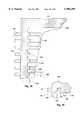
- outer leads 118A from the transfer molding processextend outwardly from the molded package 120.
- Vertical grooves 156are premolded or formed after removal from a mold.
- Each outer lead 118Ais bent upwardly at bend 118B.
- the outer end 118Cis closely fitted within the groove 156 near the top surface 117 of the molded package 120, and a portion 118D of the lead in the area of bend 118B typically extends a short distance outwardly from the groove to provide a bonding surface for lateral electrical connection to another semiconductor device, electrical conduit, or electrical apparatus.
- outer leads 118are shown as short leads like those of the embodiment of drawing FIG. 8, they may take any useful form such as the inverted-J leads illustrated in drawing FIG. 5, the lateral leads of FIG. 12, or may be eliminated as outer leads as in drawing FIGS. 10 and 11, depending upon the apparatus to which the device 100 is to be connected.
- FIG. 16shows a mold assembly 160 for encapsulating the die/lead frame assembly 162 in polymer to form the semiconductor package 120.
- the die/leadframe assembly 162is shown as including a die 102, leadframe 104, bond wires 110, and insulative tape 158.
Landscapes
- Engineering & Computer Science (AREA)
- Physics & Mathematics (AREA)
- Microelectronics & Electronic Packaging (AREA)
- Power Engineering (AREA)
- Condensed Matter Physics & Semiconductors (AREA)
- General Physics & Mathematics (AREA)
- Computer Hardware Design (AREA)
- Geometry (AREA)
- Manufacturing & Machinery (AREA)
- Lead Frames For Integrated Circuits (AREA)
- Structures Or Materials For Encapsulating Or Coating Semiconductor Devices Or Solid State Devices (AREA)
Abstract
Description
Claims (14)
Priority Applications (10)
| Application Number | Priority Date | Filing Date | Title |
|---|---|---|---|
| US08/890,414US5986209A (en) | 1997-07-09 | 1997-07-09 | Package stack via bottom leaded plastic (BLP) packaging |
| US09/330,105US6188021B1 (en) | 1997-07-09 | 1999-06-10 | Package stack via bottom leaded plastic (BLP) packaging |
| US09/336,919US6146919A (en) | 1997-07-09 | 1999-06-21 | Package stack via bottom leaded plastic (BLP) packaging |
| US09/337,628US6166328A (en) | 1997-07-09 | 1999-06-21 | Package stack via bottom leaded plastic (BLP) packaging |
| US09/336,925US6213747B1 (en) | 1997-07-09 | 1999-06-21 | Package stack via bottom leaded plastic (BLP) packaging |
| US09/641,623US6265660B1 (en) | 1997-07-09 | 2000-08-18 | Package stack via bottom leaded plastic (BLP) packaging |
| US09/819,909US6537051B2 (en) | 1997-07-09 | 2001-03-28 | Encapsulation mold with a castellated inner surface |
| US10/369,067US6899534B2 (en) | 1997-07-09 | 2003-02-18 | Mold assembly for a package stack via bottom-leaded plastic (blp) packaging |
| US11/138,756US7094046B2 (en) | 1997-07-09 | 2005-05-25 | Mold assembly for a package stack via bottom-leaded plastic (BLP) packaging |
| US11/338,384US20060118938A1 (en) | 1997-07-09 | 2006-01-24 | Mold assembly, method and a package stack via bottom-leaded plastic (BLP) packaging |
Applications Claiming Priority (1)
| Application Number | Priority Date | Filing Date | Title |
|---|---|---|---|
| US08/890,414US5986209A (en) | 1997-07-09 | 1997-07-09 | Package stack via bottom leaded plastic (BLP) packaging |
Related Child Applications (4)
| Application Number | Title | Priority Date | Filing Date |
|---|---|---|---|
| US09/330,105ContinuationUS6188021B1 (en) | 1997-07-09 | 1999-06-10 | Package stack via bottom leaded plastic (BLP) packaging |
| US09/336,919DivisionUS6146919A (en) | 1997-07-09 | 1999-06-21 | Package stack via bottom leaded plastic (BLP) packaging |
| US09/336,925DivisionUS6213747B1 (en) | 1997-07-09 | 1999-06-21 | Package stack via bottom leaded plastic (BLP) packaging |
| US09/337,628DivisionUS6166328A (en) | 1997-07-09 | 1999-06-21 | Package stack via bottom leaded plastic (BLP) packaging |
Publications (1)
| Publication Number | Publication Date |
|---|---|
| US5986209Atrue US5986209A (en) | 1999-11-16 |
Family
ID=25396645
Family Applications (10)
| Application Number | Title | Priority Date | Filing Date |
|---|---|---|---|
| US08/890,414Expired - LifetimeUS5986209A (en) | 1997-07-09 | 1997-07-09 | Package stack via bottom leaded plastic (BLP) packaging |
| US09/330,105Expired - LifetimeUS6188021B1 (en) | 1997-07-09 | 1999-06-10 | Package stack via bottom leaded plastic (BLP) packaging |
| US09/336,919Expired - LifetimeUS6146919A (en) | 1997-07-09 | 1999-06-21 | Package stack via bottom leaded plastic (BLP) packaging |
| US09/337,628Expired - LifetimeUS6166328A (en) | 1997-07-09 | 1999-06-21 | Package stack via bottom leaded plastic (BLP) packaging |
| US09/336,925Expired - LifetimeUS6213747B1 (en) | 1997-07-09 | 1999-06-21 | Package stack via bottom leaded plastic (BLP) packaging |
| US09/641,623Expired - LifetimeUS6265660B1 (en) | 1997-07-09 | 2000-08-18 | Package stack via bottom leaded plastic (BLP) packaging |
| US09/819,909Expired - LifetimeUS6537051B2 (en) | 1997-07-09 | 2001-03-28 | Encapsulation mold with a castellated inner surface |
| US10/369,067Expired - Fee RelatedUS6899534B2 (en) | 1997-07-09 | 2003-02-18 | Mold assembly for a package stack via bottom-leaded plastic (blp) packaging |
| US11/138,756Expired - Fee RelatedUS7094046B2 (en) | 1997-07-09 | 2005-05-25 | Mold assembly for a package stack via bottom-leaded plastic (BLP) packaging |
| US11/338,384AbandonedUS20060118938A1 (en) | 1997-07-09 | 2006-01-24 | Mold assembly, method and a package stack via bottom-leaded plastic (BLP) packaging |
Family Applications After (9)
| Application Number | Title | Priority Date | Filing Date |
|---|---|---|---|
| US09/330,105Expired - LifetimeUS6188021B1 (en) | 1997-07-09 | 1999-06-10 | Package stack via bottom leaded plastic (BLP) packaging |
| US09/336,919Expired - LifetimeUS6146919A (en) | 1997-07-09 | 1999-06-21 | Package stack via bottom leaded plastic (BLP) packaging |
| US09/337,628Expired - LifetimeUS6166328A (en) | 1997-07-09 | 1999-06-21 | Package stack via bottom leaded plastic (BLP) packaging |
| US09/336,925Expired - LifetimeUS6213747B1 (en) | 1997-07-09 | 1999-06-21 | Package stack via bottom leaded plastic (BLP) packaging |
| US09/641,623Expired - LifetimeUS6265660B1 (en) | 1997-07-09 | 2000-08-18 | Package stack via bottom leaded plastic (BLP) packaging |
| US09/819,909Expired - LifetimeUS6537051B2 (en) | 1997-07-09 | 2001-03-28 | Encapsulation mold with a castellated inner surface |
| US10/369,067Expired - Fee RelatedUS6899534B2 (en) | 1997-07-09 | 2003-02-18 | Mold assembly for a package stack via bottom-leaded plastic (blp) packaging |
| US11/138,756Expired - Fee RelatedUS7094046B2 (en) | 1997-07-09 | 2005-05-25 | Mold assembly for a package stack via bottom-leaded plastic (BLP) packaging |
| US11/338,384AbandonedUS20060118938A1 (en) | 1997-07-09 | 2006-01-24 | Mold assembly, method and a package stack via bottom-leaded plastic (BLP) packaging |
Country Status (1)
| Country | Link |
|---|---|
| US (10) | US5986209A (en) |
Cited By (136)
| Publication number | Priority date | Publication date | Assignee | Title |
|---|---|---|---|---|
| US6084293A (en)* | 1997-07-25 | 2000-07-04 | Oki Electric Industry Co., Ltd. | Stacked semiconductor device |
| US6242798B1 (en)* | 1996-11-22 | 2001-06-05 | Hyundai Electronics Industries Co., Ltd. | Stacked bottom lead package in semiconductor devices |
| US6320251B1 (en)* | 2000-01-18 | 2001-11-20 | Amkor Technology, Inc. | Stackable package for an integrated circuit |
| US6404046B1 (en) | 2000-02-03 | 2002-06-11 | Amkor Technology, Inc. | Module of stacked integrated circuit packages including an interposer |
| US6424031B1 (en) | 2000-05-08 | 2002-07-23 | Amkor Technology, Inc. | Stackable package with heat sink |
| US6433418B1 (en)* | 1998-07-24 | 2002-08-13 | Fujitsu Limited | Apparatus for a vertically accumulable semiconductor device with external leads secured by a positioning mechanism |
| US6448506B1 (en) | 2000-12-28 | 2002-09-10 | Amkor Technology, Inc. | Semiconductor package and circuit board for making the package |
| US20020140077A1 (en)* | 1998-02-27 | 2002-10-03 | Micron Technology, Inc. | Multichip semiconductor package |
| US6462424B1 (en)* | 1992-10-20 | 2002-10-08 | Fujitsu Limited | Semiconductor device, method of producing semiconductor device and semiconductor device mounting structure |
| US6518659B1 (en) | 2000-05-08 | 2003-02-11 | Amkor Technology, Inc. | Stackable package having a cavity and a lid for an electronic device |
| US6548376B2 (en) | 2001-08-30 | 2003-04-15 | Micron Technology, Inc. | Methods of thinning microelectronic workpieces |
| US20030071338A1 (en)* | 2001-10-16 | 2003-04-17 | Jeung Boon Suan | Apparatus and method for leadless packaging of semiconductor devices |
| US6552910B1 (en) | 2000-06-28 | 2003-04-22 | Micron Technology, Inc. | Stacked-die assemblies with a plurality of microelectronic devices and methods of manufacture |
| US6560117B2 (en) | 2000-06-28 | 2003-05-06 | Micron Technology, Inc. | Packaged microelectronic die assemblies and methods of manufacture |
| US6558600B1 (en) | 2000-05-04 | 2003-05-06 | Micron Technology, Inc. | Method for packaging microelectronic substrates |
| US6564979B2 (en) | 2001-07-18 | 2003-05-20 | Micron Technology, Inc. | Method and apparatus for dispensing adhesive on microelectronic substrate supports |
| US6564454B1 (en) | 2000-12-28 | 2003-05-20 | Amkor Technology, Inc. | Method of making and stacking a semiconductor package |
| US6576494B1 (en) | 2000-06-28 | 2003-06-10 | Micron Technology, Inc. | Recessed encapsulated microelectronic devices and methods for formation |
| US20030111718A1 (en)* | 1997-12-31 | 2003-06-19 | Kinsman Larry D. | Vertically mountable and alignable semiconductor device assembly |
| US20030129271A1 (en)* | 1997-07-09 | 2003-07-10 | Tandy Patrick W. | Package stack via bottom-leaded plastic (BLP) packaging |
| US6607937B1 (en) | 2000-08-23 | 2003-08-19 | Micron Technology, Inc. | Stacked microelectronic dies and methods for stacking microelectronic dies |
| US6622380B1 (en) | 2002-02-12 | 2003-09-23 | Micron Technology, Inc. | Methods for manufacturing microelectronic devices and methods for mounting microelectronic packages to circuit boards |
| US6638595B2 (en) | 2000-06-28 | 2003-10-28 | Micron Technology, Inc. | Method and apparatus for reduced flash encapsulation of microelectronic devices |
| US6653173B2 (en) | 2000-06-16 | 2003-11-25 | Micron Technology, Inc. | Method and apparatus for packaging a microelectronic die |
| US6656769B2 (en) | 2000-05-08 | 2003-12-02 | Micron Technology, Inc. | Method and apparatus for distributing mold material in a mold for packaging microelectronic devices |
| US6664649B2 (en)* | 2001-02-28 | 2003-12-16 | Siliconware Precision Industries Co., Ltd. | Lead-on-chip type of semiconductor package with embedded heat sink |
| US20030232462A1 (en)* | 2002-06-18 | 2003-12-18 | Poo Chia Yong | Semiconductor devices and semiconductor device components with peripherally located, castellated contacts, assemblies and packages including such semiconductor devices or packages and associated methods |
| US6667544B1 (en) | 2000-06-30 | 2003-12-23 | Amkor Technology, Inc. | Stackable package having clips for fastening package and tool for opening clips |
| US20040000703A1 (en)* | 2002-06-27 | 2004-01-01 | Jui-Chung Lee | Semiconductor package body having a lead frame with enhanced heat dissipation |
| US20040026776A1 (en)* | 2002-08-08 | 2004-02-12 | Brand Joseph M. | Microelectronic devices and methods for manufacturing and operating packaged microelectronic device assemblies |
| US20040026773A1 (en)* | 2002-08-08 | 2004-02-12 | Koon Eng Meow | Packaged microelectronic components |
| US20040031621A1 (en)* | 2002-08-19 | 2004-02-19 | Heng Puah Kia | Packaged microelectronic component assemblies |
| US20040038447A1 (en)* | 2002-08-21 | 2004-02-26 | Corisis David J | Packaged microelectronic devices and methods for assembling microelectronic devices |
| US20040035917A1 (en)* | 2002-08-22 | 2004-02-26 | Michel Koopmans | Apparatus and method for depositing and reflowing solder paste on a microelectronic workpiece |
| US6710429B2 (en)* | 2000-06-30 | 2004-03-23 | Renesas Technology Corp. | Semiconductor device and process for production thereof |
| US6750547B2 (en) | 2001-12-26 | 2004-06-15 | Micron Technology, Inc. | Multi-substrate microelectronic packages and methods for manufacture |
| US20040124523A1 (en)* | 2002-06-18 | 2004-07-01 | Poo Chia Yong | Semiconductor devices including peripherally located bond pads, intermediates thereof, assemblies, and packages including the semiconductor devices, and support elements for the semiconductor devices |
| US20040155331A1 (en)* | 2003-02-11 | 2004-08-12 | Blaine Thurgood | Packaged microelectronic devices and methods for packaging microelectronic devices |
| US6777786B2 (en)* | 2001-03-12 | 2004-08-17 | Fairchild Semiconductor Corporation | Semiconductor device including stacked dies mounted on a leadframe |
| US20040159921A1 (en)* | 2001-12-26 | 2004-08-19 | Stephen Moxham | Methods for coupling a flowable conductive material to microelectronic substrates |
| US20040173899A1 (en)* | 2003-03-04 | 2004-09-09 | Peng Neo Chee | Microelectronic component assemblies employing lead frames having reduced-thickness inner lengths |
| US20040178495A1 (en)* | 2003-03-14 | 2004-09-16 | Yean Tay Wuu | Microelectronic devices and methods for packaging microelectronic devices |
| US20040177984A1 (en)* | 2003-03-11 | 2004-09-16 | Groothuis Steven K. | Microelectronic component assemblies having lead frames adapted to reduce package bow |
| US6796028B2 (en) | 2000-08-23 | 2004-09-28 | Micron Technology, Inc. | Method of Interconnecting substrates for electrical coupling of microelectronic components |
| US20040238909A1 (en)* | 2003-05-30 | 2004-12-02 | Boon Suan Jeung | Packaged microelectronic devices and methods of packaging microelectronic devices |
| US20040251557A1 (en)* | 2003-06-16 | 2004-12-16 | Sandisk Corporation | Integrated circuit package having stacked integrated circuits and method therefor |
| US20040251523A1 (en)* | 2003-06-16 | 2004-12-16 | Sandisk Corporation | Stackable integrated circuit package and method therefor |
| US6838760B1 (en) | 2000-08-28 | 2005-01-04 | Micron Technology, Inc. | Packaged microelectronic devices with interconnecting units |
| US20050019984A1 (en)* | 2000-08-09 | 2005-01-27 | Tongbi Jiang | Multiple substrate microelectronic devices and methods of manufacture |
| US20050019988A1 (en)* | 2002-04-04 | 2005-01-27 | Tongbi Jiang | Method and apparatus for attaching microelectronic substrates and support members |
| SG108233A1 (en)* | 1999-12-20 | 2005-01-28 | Amkor Technology Inc | Stackable semiconductor package and method for manufacturing same |
| US20050026395A1 (en)* | 2002-01-16 | 2005-02-03 | Micron Technology, Inc. | Fabrication of stacked microelectronic devices |
| US20050029329A1 (en)* | 2003-08-06 | 2005-02-10 | Roberts Stuart L. | Wire bonders and methods of wire-bonding |
| US20050045378A1 (en)* | 2003-08-29 | 2005-03-03 | Heng Mung Suan | Stacked microfeature devices and associated methods |
| US20050046431A1 (en)* | 2003-09-03 | 2005-03-03 | Kirby Kyle K. | Probe card for use with microelectronic components,and methods for making same |
| US20050067680A1 (en)* | 2003-09-30 | 2005-03-31 | Boon Suan Jeung | Castellated chip-scale packages and methods for fabricating the same |
| US6876066B2 (en) | 2001-08-29 | 2005-04-05 | Micron Technology, Inc. | Packaged microelectronic devices and methods of forming same |
| US20050093174A1 (en)* | 2003-10-31 | 2005-05-05 | Seng Eric T.S. | Reduced footprint packaged microelectronic components and methods for manufacturing such microelectronic components |
| US20050093177A1 (en)* | 2003-10-29 | 2005-05-05 | Advanced Semiconductor Engineering, Inc. | Semiconductor package, method for manufacturing the same and lead frame for use in the same |
| US20050104171A1 (en)* | 2003-11-13 | 2005-05-19 | Benson Peter A. | Microelectronic devices having conductive complementary structures and methods of manufacturing microelectronic devices having conductive complementary structures |
| US20050104228A1 (en)* | 2003-11-13 | 2005-05-19 | Rigg Sidney B. | Microelectronic devices, methods for forming vias in microelectronic devices, and methods for packaging microelectronic devices |
| US20050127532A1 (en)* | 2003-12-09 | 2005-06-16 | Leeshawn Luo | Inverted J-lead package for power devices |
| US20050156300A1 (en)* | 2003-01-06 | 2005-07-21 | Micron Technology, Inc. | Microelectronic component assemblies and microelectronic component lead frame structures |
| US6921860B2 (en) | 2003-03-18 | 2005-07-26 | Micron Technology, Inc. | Microelectronic component assemblies having exposed contacts |
| US6951982B2 (en) | 2002-11-22 | 2005-10-04 | Micron Technology, Inc. | Packaged microelectronic component assemblies |
| US20050250251A1 (en)* | 2000-08-23 | 2005-11-10 | Corisis David J | Method and apparatus for decoupling conductive portions of a microelectronic device package |
| US6977431B1 (en) | 2003-11-05 | 2005-12-20 | Amkor Technology, Inc. | Stackable semiconductor package and manufacturing method thereof |
| US6979595B1 (en) | 2000-08-24 | 2005-12-27 | Micron Technology, Inc. | Packaged microelectronic devices with pressure release elements and methods for manufacturing and using such packaged microelectronic devices |
| US20060017177A1 (en)* | 2004-07-23 | 2006-01-26 | Seng Eric T S | Microelectronic component assemblies with recessed wire bonds and methods of making same |
| US20060040428A1 (en)* | 2004-08-19 | 2006-02-23 | Johnson Mark S | Conductive structures for microfeature devices and methods for fabricating microfeature devices |
| US20060043611A1 (en)* | 2004-09-01 | 2006-03-02 | Kinsman Larry D | Reduced-dimension microelectronic component assemblies with wire bonds and methods of making same |
| US20060044773A1 (en)* | 2004-08-25 | 2006-03-02 | Micron Technology, Inc. | Methods and apparatuses for transferring heat from stacked microfeature devices |
| US20060046346A1 (en)* | 2004-09-01 | 2006-03-02 | Benson Peter A | Methods for packaging microfeature devices and microfeature devices formed by such methods |
| US20060046436A1 (en)* | 2000-09-11 | 2006-03-02 | Shinji Ohuchi | Manufacturing method of stack-type semiconductor device |
| US7009296B1 (en) | 2004-01-15 | 2006-03-07 | Amkor Technology, Inc. | Semiconductor package with substrate coupled to a peripheral side surface of a semiconductor die |
| US20060051896A1 (en)* | 2004-09-09 | 2006-03-09 | Meadows Paul M | Stacking circuit elements |
| US7037756B1 (en) | 2001-08-30 | 2006-05-02 | Micron Technology, Inc. | Stacked microelectronic devices and methods of fabricating same |
| US7061120B2 (en) | 1999-05-20 | 2006-06-13 | Amkor Technology, Inc. | Stackable semiconductor package having semiconductor chip within central through hole of substrate |
| US20060138628A1 (en)* | 2004-12-24 | 2006-06-29 | Domintech Co., Ltd. | Stack chip package |
| US20060267173A1 (en)* | 2005-05-26 | 2006-11-30 | Sandisk Corporation | Integrated circuit package having stacked integrated circuits and method therefor |
| US20060292858A1 (en)* | 2002-07-18 | 2006-12-28 | Micron Technology, Inc. | Techniques to create low K ILD for beol |
| US20070045862A1 (en)* | 2005-09-01 | 2007-03-01 | Micron Technology, Inc. | Stacked microelectronic devices and methods for manufacturing microelectronic devices |
| US20070045803A1 (en)* | 2005-08-26 | 2007-03-01 | Micron Technology, Inc. | Microelectronic device packages, stacked microelectronic device packages, and methods for manufacturing microelectronic devices |
| US20070045796A1 (en)* | 2005-08-19 | 2007-03-01 | Micron Technology, Inc. | Microelectronic devices, stacked microelectronic devices, and methods for manufacturing microelectronic devices |
| US20070045872A1 (en)* | 2005-08-31 | 2007-03-01 | Fee Setho S | Microelectronic devices having intermediate contacts for connection to interposer substrates, and associated methods of packaging microelectronic devices with intermediate contacts |
| US20070045807A1 (en)* | 2005-09-01 | 2007-03-01 | Micron Technology, Inc. | Microelectronic devices and methods for manufacturing microelectronic devices |
| US20070045797A1 (en)* | 2005-08-24 | 2007-03-01 | Micron Technology, Inc. | Microelectronic devices and microelectronic support devices, and associated assemblies and methods |
| US7190071B2 (en) | 1999-05-07 | 2007-03-13 | Amkor Technology, Inc. | Semiconductor package and method for fabricating the same |
| US7198693B1 (en) | 2002-02-20 | 2007-04-03 | Micron Technology, Inc. | Microelectronic device having a plurality of stacked dies and methods for manufacturing such microelectronic assemblies |
| US20070148820A1 (en)* | 2005-12-22 | 2007-06-28 | Micron Technology, Inc. | Microelectronic devices and methods for manufacturing microelectronic devices |
| US20070145548A1 (en)* | 2003-12-22 | 2007-06-28 | Amkor Technology, Inc. | Stack-type semiconductor package and manufacturing method thereof |
| US7259451B2 (en) | 2003-08-29 | 2007-08-21 | Micron Technology, Inc. | Invertible microfeature device packages |
| EP1684348A3 (en)* | 2005-01-21 | 2007-08-29 | Chung-Hsing Tzu | Improved stack chip package |
| US20070210441A1 (en)* | 2006-03-08 | 2007-09-13 | Micron Technology, Inc. | Microelectronic device assemblies including assemblies with recurved leadframes, and associated methods |
| US7273769B1 (en) | 2000-08-16 | 2007-09-25 | Micron Technology, Inc. | Method and apparatus for removing encapsulating material from a packaged microelectronic device |
| US20070228577A1 (en)* | 2006-03-29 | 2007-10-04 | Micron Technology, Inc. | Packaged microelectronic devices recessed in support member cavities, and associated methods |
| US20080006940A1 (en)* | 2006-07-05 | 2008-01-10 | Micron Technology, Inc. | Lead frames, microelectronic devices with lead frames, and methods for manufacturing lead frames and microelectronic devices with lead frames |
| US20080012110A1 (en)* | 2006-07-17 | 2008-01-17 | Micron Technology, Inc. | Microelectronic packages with leadframes, including leadframes configured for stacked die packages, and associated systems and methods |
| USRE40112E1 (en) | 1999-05-20 | 2008-02-26 | Amkor Technology, Inc. | Semiconductor package and method for fabricating the same |
| US20080048316A1 (en)* | 2006-08-25 | 2008-02-28 | Micron Technology, Inc. | Packaged microdevices and methods for manufacturing packaged microdevices |
| US20080054437A1 (en)* | 2006-09-06 | 2008-03-06 | Samsung Electronics Co., Ltd. | Pop package and method of fabricating the same |
| US20080128900A1 (en)* | 2006-12-04 | 2008-06-05 | Micron Technology, Inc. | Packaged microelectronic devices and methods for manufacturing packaged microelectronic devices |
| US20080224329A1 (en)* | 2007-03-13 | 2008-09-18 | Micron Technology, Inc. | Packaged microelectronic devices and methods for manufacturing packaged microelectronic devices |
| US20080224291A1 (en)* | 2007-03-13 | 2008-09-18 | Micron Technology, Inc. | Packaged semiconductor components having substantially rigid support members and methods of packaging semiconductor components |
| US20080258282A1 (en)* | 2007-04-23 | 2008-10-23 | Hua Yang | Lead frame free package and method of making |
| US20080277770A1 (en)* | 2007-04-27 | 2008-11-13 | Kabushiki Kaisha Toshiba | Semiconductor device |
| US20090008677A1 (en)* | 2006-03-16 | 2009-01-08 | Fujitsu Limited | Compound semiconductor device and manufacturing method of the same |
| US20090026592A1 (en)* | 2007-07-24 | 2009-01-29 | Micron Technology, Inc. | Semiconductor dies with recesses, associated leadframes, and associated systems and methods |
| US20090026593A1 (en)* | 2007-07-24 | 2009-01-29 | Micron Technology, Inc. | Thin semiconductor die packages and associated systems and methods |
| US7518237B2 (en) | 2005-02-08 | 2009-04-14 | Micron Technology, Inc. | Microfeature systems including adhered microfeature workpieces and support members |
| US20090212415A1 (en)* | 2008-02-22 | 2009-08-27 | Lionel Chien Tay | Integrated circuit package system with external interconnects within a die platform |
| US20090242268A1 (en)* | 2008-03-31 | 2009-10-01 | Nec Electronics Corporation | Semiconductor device capable of switching operation modes |
| US7622377B2 (en) | 2005-09-01 | 2009-11-24 | Micron Technology, Inc. | Microfeature workpiece substrates having through-substrate vias, and associated methods of formation |
| US7671459B2 (en) | 2006-02-08 | 2010-03-02 | Micron Technologies, Inc. | Microelectronic devices, stacked microelectronic devices, and methods for manufacturing such devices |
| US20100059897A1 (en)* | 2008-09-11 | 2010-03-11 | Micron Technology, Inc. | Interconnect structures for stacked dies, including penetrating structures for through-silicon vias, and associated systems and methods |
| US7759221B2 (en) | 2005-12-29 | 2010-07-20 | Micron Technology, Inc. | Methods for packaging microelectronic devices and microelectronic devices formed using such methods |
| US7807505B2 (en) | 2005-08-30 | 2010-10-05 | Micron Technology, Inc. | Methods for wafer-level packaging of microfeature devices and microfeature devices formed using such methods |
| US7833456B2 (en) | 2007-02-23 | 2010-11-16 | Micron Technology, Inc. | Systems and methods for compressing an encapsulant adjacent a semiconductor workpiece |
| US7843050B2 (en) | 2007-07-24 | 2010-11-30 | Micron Technology, Inc. | Microelectronic die packages with metal leads, including metal leads for stacked die packages, and associated systems and methods |
| US7910385B2 (en) | 2006-05-12 | 2011-03-22 | Micron Technology, Inc. | Method of fabricating microelectronic devices |
| US7947529B2 (en) | 2007-08-16 | 2011-05-24 | Micron Technology, Inc. | Microelectronic die packages with leadframes, including leadframe-based interposer for stacked die packages, and associated systems and methods |
| US8084866B2 (en) | 2003-12-10 | 2011-12-27 | Micron Technology, Inc. | Microelectronic devices and methods for filling vias in microelectronic devices |
| US20130192874A1 (en)* | 2010-07-06 | 2013-08-01 | Phoenix Contact Gmbh & Co. Kg | Connecting contact |
| KR20150081155A (en) | 2014-01-03 | 2015-07-13 | 삼성전기주식회사 | Package board, method of manufacturing the same and semiconductor package using the same |
| KR20150137824A (en) | 2014-05-30 | 2015-12-09 | 삼성전기주식회사 | Package substrate, package, package on package and maunfacutring method of package substrate |
| KR20150137830A (en) | 2014-05-30 | 2015-12-09 | 삼성전기주식회사 | Package board and method for manufacturing the same |
| KR20150137829A (en) | 2014-05-30 | 2015-12-09 | 삼성전기주식회사 | Package board and method for manufacturing the same |
| KR20150142520A (en) | 2014-06-12 | 2015-12-22 | 삼성전기주식회사 | Package board and package using the same |
| KR20150142936A (en) | 2014-06-12 | 2015-12-23 | 삼성전기주식회사 | Package board and package using the same |
| KR20160008848A (en) | 2014-07-15 | 2016-01-25 | 삼성전기주식회사 | Package board, method of manufacturing the same and stack type package using the therof |
| US20160035647A1 (en)* | 2013-05-23 | 2016-02-04 | Panasonic Corporation | Semiconductor device having heat dissipation structure and laminate of semiconductor devices |
| KR20160032985A (en) | 2014-09-17 | 2016-03-25 | 삼성전기주식회사 | Package board, method for manufacturing the same and package on package having the thereof |
| KR20160046657A (en) | 2014-10-21 | 2016-04-29 | 삼성전기주식회사 | Semiconductor, method of manufacturing the same and stacked type package using therof |
| US9466545B1 (en) | 2007-02-21 | 2016-10-11 | Amkor Technology, Inc. | Semiconductor package in package |
| KR20160141516A (en) | 2015-06-01 | 2016-12-09 | 삼성전기주식회사 | Printed circuit board, method for manufacturing the same and semiconductor package having the thereof |
| US20230260879A1 (en)* | 2019-06-29 | 2023-08-17 | Texas Instruments Incorporated | Three-dimensional functional integration |
Families Citing this family (79)
| Publication number | Priority date | Publication date | Assignee | Title |
|---|---|---|---|---|
| JP4342013B2 (en)* | 1998-05-06 | 2009-10-14 | 株式会社ハイニックスセミコンダクター | BLP stack of ultra-high integrated circuit and manufacturing method thereof |
| US6323060B1 (en) | 1999-05-05 | 2001-11-27 | Dense-Pac Microsystems, Inc. | Stackable flex circuit IC package and method of making same |
| US6262895B1 (en) | 2000-01-13 | 2001-07-17 | John A. Forthun | Stackable chip package with flex carrier |
| US6787388B1 (en)* | 2000-09-07 | 2004-09-07 | Stmicroelectronics, Inc. | Surface mount package with integral electro-static charge dissipating ring using lead frame as ESD device |
| JP2002222903A (en)* | 2001-01-26 | 2002-08-09 | Mitsubishi Electric Corp | Semiconductor package and semiconductor device |
| KR100369907B1 (en)* | 2001-02-12 | 2003-01-30 | 삼성전자 주식회사 | Semiconductor Package And Mounting Structure On Substrate Thereof And Stack Structure Thereof |
| US6969918B1 (en) | 2001-08-30 | 2005-11-29 | Micron Technology, Inc. | System for fabricating semiconductor components using mold cavities having runners configured to minimize venting |
| US6956284B2 (en) | 2001-10-26 | 2005-10-18 | Staktek Group L.P. | Integrated circuit stacking system and method |
| US7310458B2 (en) | 2001-10-26 | 2007-12-18 | Staktek Group L.P. | Stacked module systems and methods |
| US7026708B2 (en) | 2001-10-26 | 2006-04-11 | Staktek Group L.P. | Low profile chip scale stacking system and method |
| US7656678B2 (en) | 2001-10-26 | 2010-02-02 | Entorian Technologies, Lp | Stacked module systems |
| US7053478B2 (en) | 2001-10-26 | 2006-05-30 | Staktek Group L.P. | Pitch change and chip scale stacking system |
| US20060255446A1 (en) | 2001-10-26 | 2006-11-16 | Staktek Group, L.P. | Stacked modules and method |
| US20030234443A1 (en) | 2001-10-26 | 2003-12-25 | Staktek Group, L.P. | Low profile stacking system and method |
| US7485951B2 (en)* | 2001-10-26 | 2009-02-03 | Entorian Technologies, Lp | Modularized die stacking system and method |
| US7371609B2 (en) | 2001-10-26 | 2008-05-13 | Staktek Group L.P. | Stacked module systems and methods |
| US7202555B2 (en) | 2001-10-26 | 2007-04-10 | Staktek Group L.P. | Pitch change and chip scale stacking system and method |
| US6940729B2 (en)* | 2001-10-26 | 2005-09-06 | Staktek Group L.P. | Integrated circuit stacking system and method |
| US6914324B2 (en) | 2001-10-26 | 2005-07-05 | Staktek Group L.P. | Memory expansion and chip scale stacking system and method |
| US7081373B2 (en) | 2001-12-14 | 2006-07-25 | Staktek Group, L.P. | CSP chip stack with flex circuit |
| JP2003204039A (en)* | 2002-01-04 | 2003-07-18 | Mitsubishi Electric Corp | Semiconductor device |
| TWI338927B (en)* | 2003-04-02 | 2011-03-11 | United Test And Assembly Ct | Multi-chip ball grid array package and method of manufacture |
| US7542304B2 (en) | 2003-09-15 | 2009-06-02 | Entorian Technologies, Lp | Memory expansion and integrated circuit stacking system and method |
| CN100370611C (en)* | 2004-02-03 | 2008-02-20 | 旺宏电子股份有限公司 | Electronic component stack structure |
| US7851899B2 (en)* | 2004-04-02 | 2010-12-14 | Utac - United Test And Assembly Test Center Ltd. | Multi-chip ball grid array package and method of manufacture |
| US6972372B1 (en)* | 2004-05-28 | 2005-12-06 | Macronix International Co., Ltd. | Method and apparatus for stacking electrical components using outer lead portions and exposed inner lead portions to provide interconnection |
| US7381593B2 (en)* | 2004-08-05 | 2008-06-03 | St Assembly Test Services Ltd. | Method and apparatus for stacked die packaging |
| US7522421B2 (en) | 2004-09-03 | 2009-04-21 | Entorian Technologies, Lp | Split core circuit module |
| US7423885B2 (en) | 2004-09-03 | 2008-09-09 | Entorian Technologies, Lp | Die module system |
| US7606049B2 (en) | 2004-09-03 | 2009-10-20 | Entorian Technologies, Lp | Module thermal management system and method |
| US7760513B2 (en) | 2004-09-03 | 2010-07-20 | Entorian Technologies Lp | Modified core for circuit module system and method |
| US7446410B2 (en)* | 2004-09-03 | 2008-11-04 | Entorian Technologies, Lp | Circuit module with thermal casing systems |
| US7468893B2 (en) | 2004-09-03 | 2008-12-23 | Entorian Technologies, Lp | Thin module system and method |
| US20060050492A1 (en) | 2004-09-03 | 2006-03-09 | Staktek Group, L.P. | Thin module system and method |
| US7579687B2 (en)* | 2004-09-03 | 2009-08-25 | Entorian Technologies, Lp | Circuit module turbulence enhancement systems and methods |
| US7616452B2 (en) | 2004-09-03 | 2009-11-10 | Entorian Technologies, Lp | Flex circuit constructions for high capacity circuit module systems and methods |
| US7542297B2 (en) | 2004-09-03 | 2009-06-02 | Entorian Technologies, Lp | Optimized mounting area circuit module system and method |
| US7324352B2 (en) | 2004-09-03 | 2008-01-29 | Staktek Group L.P. | High capacity thin module system and method |
| US7511968B2 (en) | 2004-09-03 | 2009-03-31 | Entorian Technologies, Lp | Buffered thin module system and method |
| US7606040B2 (en) | 2004-09-03 | 2009-10-20 | Entorian Technologies, Lp | Memory module system and method |
| US20060053345A1 (en)* | 2004-09-03 | 2006-03-09 | Staktek Group L.P. | Thin module system and method |
| US7443023B2 (en) | 2004-09-03 | 2008-10-28 | Entorian Technologies, Lp | High capacity thin module system |
| US7289327B2 (en) | 2006-02-27 | 2007-10-30 | Stakick Group L.P. | Active cooling methods and apparatus for modules |
| US7606050B2 (en) | 2004-09-03 | 2009-10-20 | Entorian Technologies, Lp | Compact module system and method |
| US7791180B2 (en)* | 2004-10-01 | 2010-09-07 | Yamaha Corporation | Physical quantity sensor and lead frame used for same |
| US7595548B2 (en)* | 2004-10-08 | 2009-09-29 | Yamaha Corporation | Physical quantity sensor and manufacturing method therefor |
| US7309914B2 (en) | 2005-01-20 | 2007-12-18 | Staktek Group L.P. | Inverted CSP stacking system and method |
| US8395251B2 (en)* | 2005-05-12 | 2013-03-12 | Stats Chippac Ltd. | Integrated circuit package to package stacking system |
| US7518224B2 (en)* | 2005-05-16 | 2009-04-14 | Stats Chippac Ltd. | Offset integrated circuit package-on-package stacking system |
| US7746656B2 (en)* | 2005-05-16 | 2010-06-29 | Stats Chippac Ltd. | Offset integrated circuit package-on-package stacking system |
| US7033861B1 (en) | 2005-05-18 | 2006-04-25 | Staktek Group L.P. | Stacked module systems and method |
| WO2007005263A2 (en)* | 2005-06-30 | 2007-01-11 | Fairchild Semiconductor Corporation | Semiconductor die package and method for making the same |
| US7576995B2 (en) | 2005-11-04 | 2009-08-18 | Entorian Technologies, Lp | Flex circuit apparatus and method for adding capacitance while conserving circuit board surface area |
| US7304382B2 (en) | 2006-01-11 | 2007-12-04 | Staktek Group L.P. | Managed memory component |
| US7605454B2 (en) | 2006-01-11 | 2009-10-20 | Entorian Technologies, Lp | Memory card and method for devising |
| US7508069B2 (en) | 2006-01-11 | 2009-03-24 | Entorian Technologies, Lp | Managed memory component |
| US7508058B2 (en) | 2006-01-11 | 2009-03-24 | Entorian Technologies, Lp | Stacked integrated circuit module |
| US7608920B2 (en) | 2006-01-11 | 2009-10-27 | Entorian Technologies, Lp | Memory card and method for devising |
| US7511969B2 (en) | 2006-02-02 | 2009-03-31 | Entorian Technologies, Lp | Composite core circuit module system and method |
| US7535086B2 (en)* | 2006-08-03 | 2009-05-19 | Stats Chippac Ltd. | Integrated circuit package-on-package stacking system |
| KR100833184B1 (en)* | 2006-09-21 | 2008-05-28 | 삼성전자주식회사 | Stacked Semiconductor Packages |
| US7468553B2 (en) | 2006-10-20 | 2008-12-23 | Entorian Technologies, Lp | Stackable micropackages and stacked modules |
| US7417310B2 (en) | 2006-11-02 | 2008-08-26 | Entorian Technologies, Lp | Circuit module having force resistant construction |
| US8163600B2 (en)* | 2006-12-28 | 2012-04-24 | Stats Chippac Ltd. | Bridge stack integrated circuit package-on-package system |
| US7729131B2 (en)* | 2007-01-05 | 2010-06-01 | Apple Inc. | Multiple circuit board arrangements in electronic devices |
| DE102007018914B4 (en)* | 2007-04-19 | 2019-01-17 | Infineon Technologies Ag | Semiconductor device with a semiconductor chip stack and method for producing the same |
| US20090004783A1 (en)* | 2007-06-27 | 2009-01-01 | Ming Hsun Lee | Method of package stacking using unbalanced molded tsop |
| US20090001529A1 (en)* | 2007-06-27 | 2009-01-01 | Ming Hsun Lee | Package stacking using unbalanced molded tsop |
| US7893545B2 (en)* | 2007-07-18 | 2011-02-22 | Infineon Technologies Ag | Semiconductor device |
| US7830022B2 (en)* | 2007-10-22 | 2010-11-09 | Infineon Technologies Ag | Semiconductor package |
| US9147649B2 (en)* | 2008-01-24 | 2015-09-29 | Infineon Technologies Ag | Multi-chip module |
| US20110147910A1 (en)* | 2009-12-21 | 2011-06-23 | Micron Technology, Inc. | Method for stacking die in thin, small-outline package |
| JP2012204667A (en)* | 2011-03-25 | 2012-10-22 | Toshiba Corp | Semiconductor device |
| US20150257300A1 (en)* | 2014-03-10 | 2015-09-10 | Kabushiki Kaisha Toshiba | Electronic device |
| US20160071788A1 (en)* | 2014-03-17 | 2016-03-10 | Texas Instruments Incorporated | Packaged semiconductor devices having solderable lead surfaces exposed by grooves in package compound |
| US9392691B2 (en) | 2014-07-16 | 2016-07-12 | International Business Machines Corporation | Multi-stacked electronic device with defect-free solder connection |
| US20200035577A1 (en)* | 2018-07-26 | 2020-01-30 | Texas Instruments Incorporated | Packaged integrated circuit |
| CN111090058A (en)* | 2019-11-22 | 2020-05-01 | 珠海格力电器股份有限公司 | Frame, preparation method thereof and high-temperature reverse bias test |
| EP4177941A1 (en)* | 2021-11-08 | 2023-05-10 | Nexperia B.V. | Electronic package and method for manufacturing the same |
Citations (21)
| Publication number | Priority date | Publication date | Assignee | Title |
|---|---|---|---|---|
| US5095402A (en)* | 1990-10-02 | 1992-03-10 | Rogers Corporation | Internally decoupled integrated circuit package |
| US5200364A (en)* | 1990-01-26 | 1993-04-06 | Texas Instruments Incorporated | Packaged integrated circuit with encapsulated electronic devices |
| US5214845A (en)* | 1992-05-11 | 1993-06-01 | Micron Technology, Inc. | Method for producing high speed integrated circuits |
| US5331235A (en)* | 1991-06-01 | 1994-07-19 | Goldstar Electron Co., Ltd. | Multi-chip semiconductor package |
| US5418189A (en)* | 1990-09-24 | 1995-05-23 | Texas Instruments Incorporated | Integrated circuit device and method to prevent cracking during surface mount |
| US5466887A (en)* | 1993-08-26 | 1995-11-14 | Rohm Co. Ltd. | Resin-packaged electronic component |
| US5471369A (en)* | 1993-07-09 | 1995-11-28 | Fujitsu Limited | Semiconductor device having a plurality of semiconductor chips |
| US5475259A (en)* | 1991-10-17 | 1995-12-12 | Fujitsu Limited | Semiconductor device and carrier for carrying semiconductor device |
| US5483024A (en)* | 1993-10-08 | 1996-01-09 | Texas Instruments Incorporated | High density semiconductor package |
| US5486720A (en)* | 1994-05-26 | 1996-01-23 | Analog Devices, Inc. | EMF shielding of an integrated circuit package |
| US5493153A (en)* | 1992-11-26 | 1996-02-20 | Tokyo Tungsten Co., Ltd. | Plastic-packaged semiconductor device having a heat sink matched with a plastic package |
| US5498902A (en)* | 1993-08-25 | 1996-03-12 | Seiko Epson Corporation | Semiconductor device and its manufacturing method |
| US5508565A (en)* | 1992-12-18 | 1996-04-16 | Fujitsu Limited | Semiconductor device having a plurality of chips having identical circuit arrangement sealed in package |
| US5527743A (en)* | 1993-08-18 | 1996-06-18 | Lsi Logic Corporation | Method for encapsulating an integrated circuit package |
| US5530292A (en)* | 1990-03-15 | 1996-06-25 | Fujitsu Limited | Semiconductor device having a plurality of chips |
| US5530286A (en)* | 1988-03-20 | 1996-06-25 | Hitachi, Ltd. | Semiconductor device |
| US5535509A (en)* | 1992-06-05 | 1996-07-16 | Mitsubishi Denki Kabushiki Kaisha | Method of making a lead on chip (LOC) semiconductor device |
| US5554823A (en)* | 1991-12-27 | 1996-09-10 | Rohm Co., Ltd. | Packaging device and its manufacturing method |
| US5554886A (en)* | 1994-03-30 | 1996-09-10 | Goldstar Electron Co., Ltd. | Lead frame and semiconductor package with such lead frame |
| US5572068A (en)* | 1991-05-11 | 1996-11-05 | Goldstar Electron Co., Inc. | Integrated double-chip semiconductor package and method for fabricating same |
| US5679978A (en)* | 1993-12-06 | 1997-10-21 | Fujitsu Limited | Semiconductor device having resin gate hole through substrate for resin encapsulation |
Family Cites Families (16)
| Publication number | Priority date | Publication date | Assignee | Title |
|---|---|---|---|---|
| US3404454A (en) | 1965-10-14 | 1968-10-08 | Rogers Corp | Method of making a flat flexible cable termination |
| GB8412674D0 (en) | 1984-05-18 | 1984-06-27 | British Telecomm | Integrated circuit chip carrier |
| JPS61269338A (en) | 1985-05-24 | 1986-11-28 | Hitachi Ltd | Resin-sealed semiconductor devices and molds used for their production |
| JPS6315431A (en) | 1986-07-08 | 1988-01-22 | Fujitsu Ltd | Molding die for manufacturing semiconductor device |
| US4778641A (en) | 1986-08-11 | 1988-10-18 | National Semiconductor Corporation | Method of molding a pin grid array package |
| US4954308A (en)* | 1988-03-04 | 1990-09-04 | Citizen Watch Co., Ltd. | Resin encapsulating method |
| US5172214A (en) | 1991-02-06 | 1992-12-15 | Motorola, Inc. | Leadless semiconductor device and method for making the same |
| KR930014916A (en)* | 1991-12-24 | 1993-07-23 | 김광호 | Semiconductor package |
| JP2934357B2 (en) | 1992-10-20 | 1999-08-16 | 富士通株式会社 | Semiconductor device |
| US5783134A (en)* | 1994-01-13 | 1998-07-21 | Citizen Watch Co., Ltd. | Method of resin-sealing semiconductor device |
| US5760471A (en) | 1994-04-20 | 1998-06-02 | Fujitsu Limited | Semiconductor device having an inner lead extending over a central portion of a semiconductor device sealed in a plastic package and an outer lead exposed to the outside of a side face of the plastic package |
| JPH088389A (en)* | 1994-04-20 | 1996-01-12 | Fujitsu Ltd | Semiconductor device and semiconductor device unit |
| JP2780649B2 (en)* | 1994-09-30 | 1998-07-30 | 日本電気株式会社 | Semiconductor device |
| JPH10315431A (en)* | 1997-05-20 | 1998-12-02 | Micro Tec Kk | Screen printer |
| US5986209A (en) | 1997-07-09 | 1999-11-16 | Micron Technology, Inc. | Package stack via bottom leaded plastic (BLP) packaging |
| US5923959A (en) | 1997-07-23 | 1999-07-13 | Micron Technology, Inc. | Ball grid array (BGA) encapsulation mold |
- 1997
- 1997-07-09USUS08/890,414patent/US5986209A/ennot_activeExpired - Lifetime
- 1999
- 1999-06-10USUS09/330,105patent/US6188021B1/ennot_activeExpired - Lifetime
- 1999-06-21USUS09/336,919patent/US6146919A/ennot_activeExpired - Lifetime
- 1999-06-21USUS09/337,628patent/US6166328A/ennot_activeExpired - Lifetime
- 1999-06-21USUS09/336,925patent/US6213747B1/ennot_activeExpired - Lifetime
- 2000
- 2000-08-18USUS09/641,623patent/US6265660B1/ennot_activeExpired - Lifetime
- 2001
- 2001-03-28USUS09/819,909patent/US6537051B2/ennot_activeExpired - Lifetime
- 2003
- 2003-02-18USUS10/369,067patent/US6899534B2/ennot_activeExpired - Fee Related
- 2005
- 2005-05-25USUS11/138,756patent/US7094046B2/ennot_activeExpired - Fee Related
- 2006
- 2006-01-24USUS11/338,384patent/US20060118938A1/ennot_activeAbandoned
Patent Citations (22)
| Publication number | Priority date | Publication date | Assignee | Title |
|---|---|---|---|---|
| US5530286A (en)* | 1988-03-20 | 1996-06-25 | Hitachi, Ltd. | Semiconductor device |
| US5200364A (en)* | 1990-01-26 | 1993-04-06 | Texas Instruments Incorporated | Packaged integrated circuit with encapsulated electronic devices |
| US5530292A (en)* | 1990-03-15 | 1996-06-25 | Fujitsu Limited | Semiconductor device having a plurality of chips |
| US5418189A (en)* | 1990-09-24 | 1995-05-23 | Texas Instruments Incorporated | Integrated circuit device and method to prevent cracking during surface mount |
| US5095402A (en)* | 1990-10-02 | 1992-03-10 | Rogers Corporation | Internally decoupled integrated circuit package |
| US5572068A (en)* | 1991-05-11 | 1996-11-05 | Goldstar Electron Co., Inc. | Integrated double-chip semiconductor package and method for fabricating same |
| US5331235A (en)* | 1991-06-01 | 1994-07-19 | Goldstar Electron Co., Ltd. | Multi-chip semiconductor package |
| US5475259A (en)* | 1991-10-17 | 1995-12-12 | Fujitsu Limited | Semiconductor device and carrier for carrying semiconductor device |
| US5554823A (en)* | 1991-12-27 | 1996-09-10 | Rohm Co., Ltd. | Packaging device and its manufacturing method |
| US5214845A (en)* | 1992-05-11 | 1993-06-01 | Micron Technology, Inc. | Method for producing high speed integrated circuits |
| US5535509A (en)* | 1992-06-05 | 1996-07-16 | Mitsubishi Denki Kabushiki Kaisha | Method of making a lead on chip (LOC) semiconductor device |
| US5493153A (en)* | 1992-11-26 | 1996-02-20 | Tokyo Tungsten Co., Ltd. | Plastic-packaged semiconductor device having a heat sink matched with a plastic package |
| US5508565A (en)* | 1992-12-18 | 1996-04-16 | Fujitsu Limited | Semiconductor device having a plurality of chips having identical circuit arrangement sealed in package |
| US5471369A (en)* | 1993-07-09 | 1995-11-28 | Fujitsu Limited | Semiconductor device having a plurality of semiconductor chips |
| US5527743A (en)* | 1993-08-18 | 1996-06-18 | Lsi Logic Corporation | Method for encapsulating an integrated circuit package |
| US5570272A (en)* | 1993-08-18 | 1996-10-29 | Lsi Logic Corporation | Apparatus for encapsulating an integrated circuit package |
| US5498902A (en)* | 1993-08-25 | 1996-03-12 | Seiko Epson Corporation | Semiconductor device and its manufacturing method |
| US5466887A (en)* | 1993-08-26 | 1995-11-14 | Rohm Co. Ltd. | Resin-packaged electronic component |
| US5483024A (en)* | 1993-10-08 | 1996-01-09 | Texas Instruments Incorporated | High density semiconductor package |
| US5679978A (en)* | 1993-12-06 | 1997-10-21 | Fujitsu Limited | Semiconductor device having resin gate hole through substrate for resin encapsulation |
| US5554886A (en)* | 1994-03-30 | 1996-09-10 | Goldstar Electron Co., Ltd. | Lead frame and semiconductor package with such lead frame |
| US5486720A (en)* | 1994-05-26 | 1996-01-23 | Analog Devices, Inc. | EMF shielding of an integrated circuit package |
Non-Patent Citations (1)
| Title |
|---|
| Samsung DRAM Web Page, High Density DRAMs, 2 pages.* |
Cited By (399)
| Publication number | Priority date | Publication date | Assignee | Title |
|---|---|---|---|---|
| US6462424B1 (en)* | 1992-10-20 | 2002-10-08 | Fujitsu Limited | Semiconductor device, method of producing semiconductor device and semiconductor device mounting structure |
| US6242798B1 (en)* | 1996-11-22 | 2001-06-05 | Hyundai Electronics Industries Co., Ltd. | Stacked bottom lead package in semiconductor devices |
| US20060118938A1 (en)* | 1997-07-09 | 2006-06-08 | Tandy Patrick W | Mold assembly, method and a package stack via bottom-leaded plastic (BLP) packaging |
| US6899534B2 (en) | 1997-07-09 | 2005-05-31 | Micron Technology, Inc. | Mold assembly for a package stack via bottom-leaded plastic (blp) packaging |
| US7094046B2 (en) | 1997-07-09 | 2006-08-22 | Micron Technology, Inc. | Mold assembly for a package stack via bottom-leaded plastic (BLP) packaging |
| US20030129271A1 (en)* | 1997-07-09 | 2003-07-10 | Tandy Patrick W. | Package stack via bottom-leaded plastic (BLP) packaging |
| US20050242421A1 (en)* | 1997-07-09 | 2005-11-03 | Tandy Patrick W | Mold assembly for a package stack via bottom-leaded plastic (BLP) packaging |
| US6084293A (en)* | 1997-07-25 | 2000-07-04 | Oki Electric Industry Co., Ltd. | Stacked semiconductor device |
| US6963128B2 (en)* | 1997-12-31 | 2005-11-08 | Micron Technology, Inc. | Vertically mountable and alignable semiconductor device assembly |
| US20060033190A1 (en)* | 1997-12-31 | 2006-02-16 | Kinsman Larry D | Vertically mountable and alignable semiconductor device packages and assemblies including the same |
| US20030196323A1 (en)* | 1997-12-31 | 2003-10-23 | Kinsman Larry D. | Methods for modifying a vertical surface mount package |
| US7569418B2 (en) | 1997-12-31 | 2009-08-04 | Micron Technology, Inc. | Methods for securing packaged semiconductor devices to carrier substrates |
| US20060001155A1 (en)* | 1997-12-31 | 2006-01-05 | Kinsman Larry D | Semiconductor device packages including leads with substantially planar exposed portions extending from bottom edges of the packages, and assemblies including the packages |
| US20060030072A1 (en)* | 1997-12-31 | 2006-02-09 | Kinsman Larry D | Methods for securing packaged semiconductor devices to carrier substrates |
| US20060001150A1 (en)* | 1997-12-31 | 2006-01-05 | Kinsman Larry D | Alignment devices for securing semiconductor devices to carrier substrates, and assemblies including the alignment devices |
| US20030111718A1 (en)* | 1997-12-31 | 2003-06-19 | Kinsman Larry D. | Vertically mountable and alignable semiconductor device assembly |
| US7082681B2 (en) | 1997-12-31 | 2006-08-01 | Micron Technology, Inc. | Methods for modifying a vertical surface mount package |
| US20050212143A1 (en)* | 1998-02-27 | 2005-09-29 | Micron Technology, Inc. | Multichip semiconductor package |
| US6906409B2 (en) | 1998-02-27 | 2005-06-14 | Micron Technology, Inc. | Multichip semiconductor package |
| US20020140077A1 (en)* | 1998-02-27 | 2002-10-03 | Micron Technology, Inc. | Multichip semiconductor package |
| US6433418B1 (en)* | 1998-07-24 | 2002-08-13 | Fujitsu Limited | Apparatus for a vertically accumulable semiconductor device with external leads secured by a positioning mechanism |
| US7190071B2 (en) | 1999-05-07 | 2007-03-13 | Amkor Technology, Inc. | Semiconductor package and method for fabricating the same |
| US7061120B2 (en) | 1999-05-20 | 2006-06-13 | Amkor Technology, Inc. | Stackable semiconductor package having semiconductor chip within central through hole of substrate |
| USRE40112E1 (en) | 1999-05-20 | 2008-02-26 | Amkor Technology, Inc. | Semiconductor package and method for fabricating the same |
| SG108233A1 (en)* | 1999-12-20 | 2005-01-28 | Amkor Technology Inc | Stackable semiconductor package and method for manufacturing same |
| US6320251B1 (en)* | 2000-01-18 | 2001-11-20 | Amkor Technology, Inc. | Stackable package for an integrated circuit |
| US6404046B1 (en) | 2000-02-03 | 2002-06-11 | Amkor Technology, Inc. | Module of stacked integrated circuit packages including an interposer |
| US6558600B1 (en) | 2000-05-04 | 2003-05-06 | Micron Technology, Inc. | Method for packaging microelectronic substrates |
| US20030209831A1 (en)* | 2000-05-04 | 2003-11-13 | Williams Vernon M. | Method and apparatus for packaging microelectronic substrates |
| US6518659B1 (en) | 2000-05-08 | 2003-02-11 | Amkor Technology, Inc. | Stackable package having a cavity and a lid for an electronic device |
| US6656769B2 (en) | 2000-05-08 | 2003-12-02 | Micron Technology, Inc. | Method and apparatus for distributing mold material in a mold for packaging microelectronic devices |
| US6424031B1 (en) | 2000-05-08 | 2002-07-23 | Amkor Technology, Inc. | Stackable package with heat sink |
| US6653173B2 (en) | 2000-06-16 | 2003-11-25 | Micron Technology, Inc. | Method and apparatus for packaging a microelectronic die |
| US6664139B2 (en) | 2000-06-16 | 2003-12-16 | Micron Technology, Inc. | Method and apparatus for packaging a microelectronic die |
| US6683388B2 (en) | 2000-06-16 | 2004-01-27 | Micron Technology, Inc. | Method and apparatus for packaging a microelectronic die |
| US6677675B2 (en) | 2000-06-16 | 2004-01-13 | Micron Technology, Inc. | Microelectronic devices and microelectronic die packages |
| US6644949B2 (en) | 2000-06-28 | 2003-11-11 | Micron Technology, Inc. | Apparatus for reduced flash encapsulation of microelectronic devices |
| US6841423B2 (en) | 2000-06-28 | 2005-01-11 | Micron Technology, Inc. | Methods for formation of recessed encapsulated microelectronic devices |
| US6576494B1 (en) | 2000-06-28 | 2003-06-10 | Micron Technology, Inc. | Recessed encapsulated microelectronic devices and methods for formation |
| US6819003B2 (en) | 2000-06-28 | 2004-11-16 | Micron Technology Inc. | Recessed encapsulated microelectronic devices and methods for formation |
| US6560117B2 (en) | 2000-06-28 | 2003-05-06 | Micron Technology, Inc. | Packaged microelectronic die assemblies and methods of manufacture |
| US6552910B1 (en) | 2000-06-28 | 2003-04-22 | Micron Technology, Inc. | Stacked-die assemblies with a plurality of microelectronic devices and methods of manufacture |
| US6638595B2 (en) | 2000-06-28 | 2003-10-28 | Micron Technology, Inc. | Method and apparatus for reduced flash encapsulation of microelectronic devices |
| US6667544B1 (en) | 2000-06-30 | 2003-12-23 | Amkor Technology, Inc. | Stackable package having clips for fastening package and tool for opening clips |
| US6710429B2 (en)* | 2000-06-30 | 2004-03-23 | Renesas Technology Corp. | Semiconductor device and process for production thereof |
| US20050019984A1 (en)* | 2000-08-09 | 2005-01-27 | Tongbi Jiang | Multiple substrate microelectronic devices and methods of manufacture |
| US7253025B2 (en) | 2000-08-09 | 2007-08-07 | Micron Technology, Inc. | Multiple substrate microelectronic devices and methods of manufacture |
| US7298031B1 (en) | 2000-08-09 | 2007-11-20 | Micron Technology, Inc. | Multiple substrate microelectronic devices and methods of manufacture |
| US7273769B1 (en) | 2000-08-16 | 2007-09-25 | Micron Technology, Inc. | Method and apparatus for removing encapsulating material from a packaged microelectronic device |
| US7405487B2 (en) | 2000-08-16 | 2008-07-29 | Micron Technology, Inc. | Method and apparatus for removing encapsulating material from a packaged microelectronic device |
| US7235871B2 (en) | 2000-08-23 | 2007-06-26 | Micron Technology, Inc. | Stacked microelectronic dies |
| US6607937B1 (en) | 2000-08-23 | 2003-08-19 | Micron Technology, Inc. | Stacked microelectronic dies and methods for stacking microelectronic dies |
| US6983551B2 (en) | 2000-08-23 | 2006-01-10 | Micron Technology, Inc. | Interconnecting substrates for electrical coupling of microelectronic components |
| US6982386B2 (en) | 2000-08-23 | 2006-01-03 | Micron Technology, Inc. | Interconnecting substrates for electrical coupling of microelectronic components |
| US8587109B2 (en) | 2000-08-23 | 2013-11-19 | Micron Technology, Inc. | Stacked microelectronic dies and methods for stacking microelectronic dies |
| US20050250251A1 (en)* | 2000-08-23 | 2005-11-10 | Corisis David J | Method and apparatus for decoupling conductive portions of a microelectronic device package |
| US20070052087A1 (en)* | 2000-08-23 | 2007-03-08 | Micron Technology, Inc. | Method and apparatus for decoupling conductive portions of a microelectronic device package |
| US7378723B2 (en) | 2000-08-23 | 2008-05-27 | Micron Technology, Inc. | Method and apparatus for decoupling conductive portions of a microelectronic device package |
| US8067827B2 (en) | 2000-08-23 | 2011-11-29 | Micron Technology, Inc. | Stacked microelectronic device assemblies |
| US7183138B2 (en) | 2000-08-23 | 2007-02-27 | Micron Technology, Inc. | Method and apparatus for decoupling conductive portions of a microelectronic device package |
| US6796028B2 (en) | 2000-08-23 | 2004-09-28 | Micron Technology, Inc. | Method of Interconnecting substrates for electrical coupling of microelectronic components |
| US20040038449A1 (en)* | 2000-08-23 | 2004-02-26 | Corisis David J. | Stacked microelectronic dies and methods for stacking microelectronic dies |
| US20070210435A1 (en)* | 2000-08-23 | 2007-09-13 | Micron Technology, Inc. | Stacked microelectronic dies and methods for stacking microelectronic dies |
| US7049685B2 (en) | 2000-08-24 | 2006-05-23 | Micron Technology, Inc. | Packaged microelectronic devices with pressure release elements and methods for manufacturing and using such packaged microelectronic devices |
| US6979595B1 (en) | 2000-08-24 | 2005-12-27 | Micron Technology, Inc. | Packaged microelectronic devices with pressure release elements and methods for manufacturing and using such packaged microelectronic devices |
| US6838760B1 (en) | 2000-08-28 | 2005-01-04 | Micron Technology, Inc. | Packaged microelectronic devices with interconnecting units |
| US7101737B2 (en) | 2000-08-28 | 2006-09-05 | Micron Technology, Inc. | Method of encapsulating interconnecting units in packaged microelectronic devices |
| US7332376B2 (en) | 2000-08-28 | 2008-02-19 | Micron Technology, Inc. | Method of encapsulating packaged microelectronic devices with a barrier |
| US20060046436A1 (en)* | 2000-09-11 | 2006-03-02 | Shinji Ohuchi | Manufacturing method of stack-type semiconductor device |
| US7405138B2 (en) | 2000-09-11 | 2008-07-29 | Oki Electric Industry Co., Ltd. | Manufacturing method of stack-type semiconductor device |
| US7019397B2 (en)* | 2000-09-11 | 2006-03-28 | Oki Electric Industry Co., Ltd. | Semiconductor device, manufacturing method of semiconductor device, stack type semiconductor device, and manufacturing method of stack type semiconductor device |
| US6564454B1 (en) | 2000-12-28 | 2003-05-20 | Amkor Technology, Inc. | Method of making and stacking a semiconductor package |
| US6448506B1 (en) | 2000-12-28 | 2002-09-10 | Amkor Technology, Inc. | Semiconductor package and circuit board for making the package |
| US6664649B2 (en)* | 2001-02-28 | 2003-12-16 | Siliconware Precision Industries Co., Ltd. | Lead-on-chip type of semiconductor package with embedded heat sink |
| US7071033B2 (en) | 2001-03-12 | 2006-07-04 | Fairchild Semiconductor Corporation | Method for forming semiconductor device including stacked dies |
| US20050001293A1 (en)* | 2001-03-12 | 2005-01-06 | Fairchild Semiconductor Corporation | Method for forming semiconductor device including stacked dies |
| US6777786B2 (en)* | 2001-03-12 | 2004-08-17 | Fairchild Semiconductor Corporation | Semiconductor device including stacked dies mounted on a leadframe |
| US6564979B2 (en) | 2001-07-18 | 2003-05-20 | Micron Technology, Inc. | Method and apparatus for dispensing adhesive on microelectronic substrate supports |
| US6943450B2 (en) | 2001-08-29 | 2005-09-13 | Micron Technology, Inc. | Packaged microelectronic devices and methods of forming same |
| US6876066B2 (en) | 2001-08-29 | 2005-04-05 | Micron Technology, Inc. | Packaged microelectronic devices and methods of forming same |
| US7037756B1 (en) | 2001-08-30 | 2006-05-02 | Micron Technology, Inc. | Stacked microelectronic devices and methods of fabricating same |
| US6548376B2 (en) | 2001-08-30 | 2003-04-15 | Micron Technology, Inc. | Methods of thinning microelectronic workpieces |
| US6747348B2 (en) | 2001-10-16 | 2004-06-08 | Micron Technology, Inc. | Apparatus and method for leadless packaging of semiconductor devices |
| US20030071338A1 (en)* | 2001-10-16 | 2003-04-17 | Jeung Boon Suan | Apparatus and method for leadless packaging of semiconductor devices |
| US6787894B2 (en) | 2001-10-16 | 2004-09-07 | Micron Technology, Inc. | Apparatus and method for leadless packaging of semiconductor devices |
| US6790706B2 (en) | 2001-10-16 | 2004-09-14 | Micron Technology, Inc. | Apparatus and method for leadless packaging of semiconductor devices |
| US20030071341A1 (en)* | 2001-10-16 | 2003-04-17 | Jeung Boon Suan | Apparatus and method for leadless packaging of semiconductor devices |
| US20030080403A1 (en)* | 2001-10-16 | 2003-05-01 | Jeung Boon Suan | Apparatus and method for leadless packaging of semiconductor devices |
| US6743696B2 (en) | 2001-10-16 | 2004-06-01 | Micron Technology, Inc. | Apparatus and method for leadless packaging of semiconductor devices |
| US6750547B2 (en) | 2001-12-26 | 2004-06-15 | Micron Technology, Inc. | Multi-substrate microelectronic packages and methods for manufacture |
| US20040159921A1 (en)* | 2001-12-26 | 2004-08-19 | Stephen Moxham | Methods for coupling a flowable conductive material to microelectronic substrates |
| US20040183207A1 (en)* | 2001-12-26 | 2004-09-23 | Jeung Boon Suan | Multi-substrate microelectronic packages and methods for manufacture |
| US20050242437A1 (en)* | 2001-12-26 | 2005-11-03 | Micron Technology, Inc. | Method and apparatus for supporting microelectronic substrates |
| US20040159946A1 (en)* | 2001-12-26 | 2004-08-19 | Stephen Moxham | Microelectronic assemblies, electronic devices, and apparatuses for supporting microelectronic substrates |
| US6841418B2 (en) | 2001-12-26 | 2005-01-11 | Micron Technology, Inc. | Multi-substrate microelectronic packages and methods for manufacture |
| US6870276B1 (en) | 2001-12-26 | 2005-03-22 | Micron Technology, Inc. | Apparatus for supporting microelectronic substrates |
| US6936916B2 (en) | 2001-12-26 | 2005-08-30 | Micron Technology, Inc. | Microelectronic assemblies and electronic devices including connection structures with multiple elongated members |
| US6995026B2 (en) | 2001-12-26 | 2006-02-07 | Micron Technology, Inc. | Methods for coupling a flowable conductive material to microelectronic substrates |
| US20050026395A1 (en)* | 2002-01-16 | 2005-02-03 | Micron Technology, Inc. | Fabrication of stacked microelectronic devices |
| US20060172510A1 (en)* | 2002-01-16 | 2006-08-03 | Micron Technology, Inc. | Fabrication of stacked microelectronic devices |
| US20060159947A1 (en)* | 2002-01-16 | 2006-07-20 | Micron Technology, Inc. | Fabrication of stacked microelectronic devices |
| US7037751B2 (en) | 2002-01-16 | 2006-05-02 | Micron Technology, Inc. | Fabrication of stacked microelectronic devices |
| US20050026415A1 (en)* | 2002-01-16 | 2005-02-03 | Micron Technology, Inc. | Fabrication of stacked microelectronic devices |
| US7022418B2 (en) | 2002-01-16 | 2006-04-04 | Micron Technology, Inc. | Fabrication of stacked microelectronic devices |
| US6896760B1 (en) | 2002-01-16 | 2005-05-24 | Micron Technology, Inc. | Fabrication of stacked microelectronic devices |
| US7122905B2 (en) | 2002-02-12 | 2006-10-17 | Micron Technology, Inc. | Microelectronic devices and methods for mounting microelectronic packages to circuit boards |
| US6622380B1 (en) | 2002-02-12 | 2003-09-23 | Micron Technology, Inc. | Methods for manufacturing microelectronic devices and methods for mounting microelectronic packages to circuit boards |
| US7198693B1 (en) | 2002-02-20 | 2007-04-03 | Micron Technology, Inc. | Microelectronic device having a plurality of stacked dies and methods for manufacturing such microelectronic assemblies |
| US7091064B2 (en) | 2002-04-04 | 2006-08-15 | Micron Technology, Inc. | Method and apparatus for attaching microelectronic substrates and support members |
| US7615871B2 (en) | 2002-04-04 | 2009-11-10 | Micron Technology, Inc. | Method and apparatus for attaching microelectronic substrates and support members |
| US7109588B2 (en) | 2002-04-04 | 2006-09-19 | Micron Technology, Inc. | Method and apparatus for attaching microelectronic substrates and support members |
| US20050019988A1 (en)* | 2002-04-04 | 2005-01-27 | Tongbi Jiang | Method and apparatus for attaching microelectronic substrates and support members |
| US20030232462A1 (en)* | 2002-06-18 | 2003-12-18 | Poo Chia Yong | Semiconductor devices and semiconductor device components with peripherally located, castellated contacts, assemblies and packages including such semiconductor devices or packages and associated methods |
| US20040124523A1 (en)* | 2002-06-18 | 2004-07-01 | Poo Chia Yong | Semiconductor devices including peripherally located bond pads, intermediates thereof, assemblies, and packages including the semiconductor devices, and support elements for the semiconductor devices |
| US20060208351A1 (en)* | 2002-06-18 | 2006-09-21 | Poo Chia Y | Semiconductor devices including peripherally located bond pads, intermediates thereof, and assemblies and packages including the semiconductor devices |
| US7115984B2 (en) | 2002-06-18 | 2006-10-03 | Micron Technology, Inc. | Semiconductor devices including peripherally located bond pads, intermediates thereof, assemblies, and packages including the semiconductor devices, and support elements for the semiconductor devices |
| US20060208350A1 (en)* | 2002-06-18 | 2006-09-21 | Poo Chia Y | Support elements for semiconductor devices with peripherally located bond pads |
| US7226809B2 (en) | 2002-06-18 | 2007-06-05 | Micron Technology, Inc. | Semiconductor devices and semiconductor device components with peripherally located, castellated contacts, assemblies and packages including such semiconductor devices or packages and associated methods |
| US7285850B2 (en) | 2002-06-18 | 2007-10-23 | Micron Technology, Inc. | Support elements for semiconductor devices with peripherally located bond pads |
| US20040000703A1 (en)* | 2002-06-27 | 2004-01-01 | Jui-Chung Lee | Semiconductor package body having a lead frame with enhanced heat dissipation |
| US20060292858A1 (en)* | 2002-07-18 | 2006-12-28 | Micron Technology, Inc. | Techniques to create low K ILD for beol |
| US8637973B2 (en) | 2002-08-08 | 2014-01-28 | Micron Technology, Inc. | Packaged microelectronic components with terminals exposed through encapsulant |
| US6836009B2 (en) | 2002-08-08 | 2004-12-28 | Micron Technology, Inc. | Packaged microelectronic components |
| US20060040422A1 (en)* | 2002-08-08 | 2006-02-23 | Micron Technology, Inc. | Microelectronic devices and methods for manufacturing and operating packaged microelectronic device |
| US7067905B2 (en) | 2002-08-08 | 2006-06-27 | Micron Technology, Inc. | Packaged microelectronic devices including first and second casings |
| US7306974B2 (en) | 2002-08-08 | 2007-12-11 | Micron Technology, Inc. | Microelectronic devices and methods for manufacturing and operating packaged microelectronic device assemblies |
| US7195957B2 (en) | 2002-08-08 | 2007-03-27 | Micron Technology, Inc. | Packaged microelectronic components |
| US9418872B2 (en) | 2002-08-08 | 2016-08-16 | Micron Technology, Inc. | Packaged microelectronic components |
| US20040026773A1 (en)* | 2002-08-08 | 2004-02-12 | Koon Eng Meow | Packaged microelectronic components |
| US20040026776A1 (en)* | 2002-08-08 | 2004-02-12 | Brand Joseph M. | Microelectronic devices and methods for manufacturing and operating packaged microelectronic device assemblies |
| US20040191964A1 (en)* | 2002-08-19 | 2004-09-30 | Heng Puah Kia | Packaged microelectronic component assemblies |
| US6781066B2 (en) | 2002-08-19 | 2004-08-24 | Micron Technology, Inc. | Packaged microelectronic component assemblies |
| US20040031621A1 (en)* | 2002-08-19 | 2004-02-19 | Heng Puah Kia | Packaged microelectronic component assemblies |
| US6933170B2 (en) | 2002-08-19 | 2005-08-23 | Micron Technology, Inc. | Packaged microelectronic component assemblies |
| US6924550B2 (en) | 2002-08-21 | 2005-08-02 | Micron Technology, Inc. | Packaged microelectronic devices and methods for assembling microelectronic devices |
| US6740546B2 (en) | 2002-08-21 | 2004-05-25 | Micron Technology, Inc. | Packaged microelectronic devices and methods for assembling microelectronic devices |
| US20040038447A1 (en)* | 2002-08-21 | 2004-02-26 | Corisis David J | Packaged microelectronic devices and methods for assembling microelectronic devices |
| US20040188820A1 (en)* | 2002-08-21 | 2004-09-30 | Corisis David J | Packaged microelectronic devices and methods for assembling microelectronic devices |
| US7347348B2 (en) | 2002-08-22 | 2008-03-25 | Micron Technology, Inc. | Apparatus and method for depositing and reflowing solder paste on a microelectronic workpiece |
| US20040035917A1 (en)* | 2002-08-22 | 2004-02-26 | Michel Koopmans | Apparatus and method for depositing and reflowing solder paste on a microelectronic workpiece |
| US20050092810A1 (en)* | 2002-08-22 | 2005-05-05 | Michel Koopmans | Apparatus and method for depositing and reflowing solder paste on a microelectronic workpiece |
| US6845901B2 (en) | 2002-08-22 | 2005-01-25 | Micron Technology, Inc. | Apparatus and method for depositing and reflowing solder paste on a microelectronic workpiece |
| US20080164298A1 (en)* | 2002-08-22 | 2008-07-10 | Micron Technology, Inc. | Apparatus and method for depositing and reflowing solder paste on a microelectronic workpiece |
| US7637412B2 (en) | 2002-08-22 | 2009-12-29 | Micron Technology, Inc. | Apparatus and method for depositing and reflowing solder paste on a microelectronic workpiece |
| US6951982B2 (en) | 2002-11-22 | 2005-10-04 | Micron Technology, Inc. | Packaged microelectronic component assemblies |
| US20080067644A1 (en)* | 2003-01-06 | 2008-03-20 | Micron Technology, Inc. | Microelectronic component assemblies and microelectronic component lead frame structures |
| US7298025B2 (en) | 2003-01-06 | 2007-11-20 | Micron Technology, Inc. | Microelectronic component assemblies and microelectronic component lead frame structures |
| US7923824B2 (en) | 2003-01-06 | 2011-04-12 | Micron Technology, Inc. | Microelectronic component assemblies and microelectronic component lead frame structures |
| US7247520B2 (en) | 2003-01-06 | 2007-07-24 | Micron Technology, Inc. | Microelectronic component assemblies and microelectronic component lead frame structures |
| US20050156300A1 (en)* | 2003-01-06 | 2005-07-21 | Micron Technology, Inc. | Microelectronic component assemblies and microelectronic component lead frame structures |
| US7132734B2 (en) | 2003-01-06 | 2006-11-07 | Micron Technology, Inc. | Microelectronic component assemblies and microelectronic component lead frame structures |
| US7652365B2 (en) | 2003-01-06 | 2010-01-26 | Micron Technologies, Inc. | Microelectronic component assemblies and microelectronic component lead frame structures |
| US20050156294A1 (en)* | 2003-01-06 | 2005-07-21 | Micron Technology, Inc. | Microelectronic component assemblies and microelectronic component lead frame structures |
| US6879050B2 (en) | 2003-02-11 | 2005-04-12 | Micron Technology, Inc. | Packaged microelectronic devices and methods for packaging microelectronic devices |
| US20040155331A1 (en)* | 2003-02-11 | 2004-08-12 | Blaine Thurgood | Packaged microelectronic devices and methods for packaging microelectronic devices |
| US7691680B2 (en) | 2003-03-04 | 2010-04-06 | Micron Technologies, Inc. | Method of fabricating microelectronic component assemblies employing lead frames having reduced-thickness inner lengths |
| US20080233684A1 (en)* | 2003-03-04 | 2008-09-25 | Micron Technology, Inc. | Microelectronic component assemblies employing lead frames having reduced-thickness inner lengths |
| US7425470B2 (en) | 2003-03-04 | 2008-09-16 | Micron Technology, Inc. | Microelectronic component assemblies employing lead frames having reduced-thickness inner lengths |
| US7057281B2 (en) | 2003-03-04 | 2006-06-06 | Micron Technology Inc. | Microelectronic component assemblies employing lead frames having reduced-thickness inner lengths |
| US20040173899A1 (en)* | 2003-03-04 | 2004-09-09 | Peng Neo Chee | Microelectronic component assemblies employing lead frames having reduced-thickness inner lengths |
| US7183485B2 (en) | 2003-03-11 | 2007-02-27 | Micron Technology, Inc. | Microelectronic component assemblies having lead frames adapted to reduce package bow |
| US20070128770A1 (en)* | 2003-03-11 | 2007-06-07 | Micron Technology, Inc. | Microelectronic component assemblies having lead frames adapted to reduce package bow |
| US20040177984A1 (en)* | 2003-03-11 | 2004-09-16 | Groothuis Steven K. | Microelectronic component assemblies having lead frames adapted to reduce package bow |
| US7145228B2 (en) | 2003-03-14 | 2006-12-05 | Micron Technology, Inc. | Microelectronic devices |
| US20040178495A1 (en)* | 2003-03-14 | 2004-09-16 | Yean Tay Wuu | Microelectronic devices and methods for packaging microelectronic devices |
| US20070128737A1 (en)* | 2003-03-14 | 2007-06-07 | Micron Technology, Inc. | Microelectronic devices and methods for packaging microelectronic devices |
| US20060006534A1 (en)* | 2003-03-14 | 2006-01-12 | Yean Tay W | Microelectronic devices and methods for packaging microelectronic devices |
| US6946325B2 (en) | 2003-03-14 | 2005-09-20 | Micron Technology, Inc. | Methods for packaging microelectronic devices |
| US7754531B2 (en) | 2003-03-14 | 2010-07-13 | Micron Technology, Inc. | Method for packaging microelectronic devices |
| US6921860B2 (en) | 2003-03-18 | 2005-07-26 | Micron Technology, Inc. | Microelectronic component assemblies having exposed contacts |
| US6882021B2 (en) | 2003-05-30 | 2005-04-19 | Micron Technology, Inc. | Packaged image sensing microelectronic devices including a lead and methods of packaging image sensing microelectronic devices including a lead |
| US20040238909A1 (en)* | 2003-05-30 | 2004-12-02 | Boon Suan Jeung | Packaged microelectronic devices and methods of packaging microelectronic devices |
| US7309923B2 (en) | 2003-06-16 | 2007-12-18 | Sandisk Corporation | Integrated circuit package having stacked integrated circuits and method therefor |
| US20040251557A1 (en)* | 2003-06-16 | 2004-12-16 | Sandisk Corporation | Integrated circuit package having stacked integrated circuits and method therefor |
| US6984881B2 (en)* | 2003-06-16 | 2006-01-10 | Sandisk Corporation | Stackable integrated circuit package and method therefor |
| US20040251523A1 (en)* | 2003-06-16 | 2004-12-16 | Sandisk Corporation | Stackable integrated circuit package and method therefor |
| US7227095B2 (en) | 2003-08-06 | 2007-06-05 | Micron Technology, Inc. | Wire bonders and methods of wire-bonding |
| US20050029329A1 (en)* | 2003-08-06 | 2005-02-10 | Roberts Stuart L. | Wire bonders and methods of wire-bonding |
| US7977597B2 (en) | 2003-08-06 | 2011-07-12 | Micron Technology, Inc. | Wire bonders and methods of wire-bonding |
| US10062667B2 (en) | 2003-08-29 | 2018-08-28 | Micron Technology, Inc. | Stacked microfeature devices and associated methods |
| US7742313B2 (en) | 2003-08-29 | 2010-06-22 | Micron Technology, Inc. | Stacked microfeature devices |
| US9515046B2 (en) | 2003-08-29 | 2016-12-06 | Micron Technology, Inc. | Stacked microfeature devices and associated methods |
| US20100258939A1 (en)* | 2003-08-29 | 2010-10-14 | Micron Technology, Inc. | Stacked microfeature devices and associated methods |
| US11373979B2 (en) | 2003-08-29 | 2022-06-28 | Micron Technology, Inc. | Stacked microfeature devices and associated methods |
| US20050045378A1 (en)* | 2003-08-29 | 2005-03-03 | Heng Mung Suan | Stacked microfeature devices and associated methods |
| US11887970B2 (en) | 2003-08-29 | 2024-01-30 | Micron Technology, Inc. | Stacked microfeature devices and associated methods |
| US8400780B2 (en) | 2003-08-29 | 2013-03-19 | Micron Technology, Inc. | Stacked microfeature devices |
| US7368810B2 (en) | 2003-08-29 | 2008-05-06 | Micron Technology, Inc. | Invertible microfeature device packages |
| US7071421B2 (en) | 2003-08-29 | 2006-07-04 | Micron Technology, Inc. | Stacked microfeature devices and associated methods |
| US7259451B2 (en) | 2003-08-29 | 2007-08-21 | Micron Technology, Inc. | Invertible microfeature device packages |
| US6924655B2 (en) | 2003-09-03 | 2005-08-02 | Micron Technology, Inc. | Probe card for use with microelectronic components, and methods for making same |
| US20050046431A1 (en)* | 2003-09-03 | 2005-03-03 | Kirby Kyle K. | Probe card for use with microelectronic components,and methods for making same |
| US7633159B2 (en) | 2003-09-30 | 2009-12-15 | Micron Technology, Inc. | Semiconductor device assemblies and packages with edge contacts and sacrificial substrates and other intermediate structures used or formed in fabricating the assemblies or packages |
| US20050067680A1 (en)* | 2003-09-30 | 2005-03-31 | Boon Suan Jeung | Castellated chip-scale packages and methods for fabricating the same |
| US20060006521A1 (en)* | 2003-09-30 | 2006-01-12 | Boon Suan J | Semiconductor device assemblies and packages with edge contacts and sacrificial substrates and other intermediate structures used or formed in fabricating the assemblies or packages |
| US7208335B2 (en) | 2003-09-30 | 2007-04-24 | Micron Technology, Inc. | Castellated chip-scale packages and methods for fabricating the same |
| US8063493B2 (en) | 2003-09-30 | 2011-11-22 | Micron Technology, Inc. | Semiconductor device assemblies and packages |
| US20100072603A1 (en)* | 2003-09-30 | 2010-03-25 | Micron Technology, Inc. | Semiconductor device assemblies and packages with edge contacts and sacrificial substrates and other intermediate structures used or formed in fabricating the assemblies or packages |
| SG120123A1 (en)* | 2003-09-30 | 2006-03-28 | Micron Technology Inc | Castellated chip-scale packages and methods for fabricating the same |
| US20050093177A1 (en)* | 2003-10-29 | 2005-05-05 | Advanced Semiconductor Engineering, Inc. | Semiconductor package, method for manufacturing the same and lead frame for use in the same |
| US7425755B2 (en)* | 2003-10-29 | 2008-09-16 | Advanced Semiconductor Engineering Inc. | Semiconductor package, method for manufacturing the same and lead frame for use in the same |
| US7218001B2 (en) | 2003-10-31 | 2007-05-15 | Micron Technology, Inc. | Reduced footprint packaged microelectronic components and methods for manufacturing such microelectronic components |
| US20050093174A1 (en)* | 2003-10-31 | 2005-05-05 | Seng Eric T.S. | Reduced footprint packaged microelectronic components and methods for manufacturing such microelectronic components |
| US7691726B2 (en) | 2003-10-31 | 2010-04-06 | Micron Technology, Inc. | Reduced footprint packaged microelectronic components and methods for manufacturing such microelectronic components |
| US6977431B1 (en) | 2003-11-05 | 2005-12-20 | Amkor Technology, Inc. | Stackable semiconductor package and manufacturing method thereof |
| US9653420B2 (en) | 2003-11-13 | 2017-05-16 | Micron Technology, Inc. | Microelectronic devices and methods for filling vias in microelectronic devices |
| US20050104171A1 (en)* | 2003-11-13 | 2005-05-19 | Benson Peter A. | Microelectronic devices having conductive complementary structures and methods of manufacturing microelectronic devices having conductive complementary structures |
| US7759800B2 (en) | 2003-11-13 | 2010-07-20 | Micron Technology, Inc. | Microelectronics devices, having vias, and packaged microelectronic devices having vias |
| US7091124B2 (en) | 2003-11-13 | 2006-08-15 | Micron Technology, Inc. | Methods for forming vias in microelectronic devices, and methods for packaging microelectronic devices |
| US20050104228A1 (en)* | 2003-11-13 | 2005-05-19 | Rigg Sidney B. | Microelectronic devices, methods for forming vias in microelectronic devices, and methods for packaging microelectronic devices |
| US7413979B2 (en) | 2003-11-13 | 2008-08-19 | Micron Technology, Inc. | Methods for forming vias in microelectronic devices, and methods for packaging microelectronic devices |
| US7633140B2 (en)* | 2003-12-09 | 2009-12-15 | Alpha And Omega Semiconductor Incorporated | Inverted J-lead for power devices |
| US20050127532A1 (en)* | 2003-12-09 | 2005-06-16 | Leeshawn Luo | Inverted J-lead package for power devices |
| US8084866B2 (en) | 2003-12-10 | 2011-12-27 | Micron Technology, Inc. | Microelectronic devices and methods for filling vias in microelectronic devices |
| US8748311B2 (en) | 2003-12-10 | 2014-06-10 | Micron Technology, Inc. | Microelectronic devices and methods for filing vias in microelectronic devices |
| US11177175B2 (en) | 2003-12-10 | 2021-11-16 | Micron Technology, Inc. | Microelectronic devices and methods for filling vias in microelectronic devices |
| US20070145548A1 (en)* | 2003-12-22 | 2007-06-28 | Amkor Technology, Inc. | Stack-type semiconductor package and manufacturing method thereof |
| US7009296B1 (en) | 2004-01-15 | 2006-03-07 | Amkor Technology, Inc. | Semiconductor package with substrate coupled to a peripheral side surface of a semiconductor die |
| US20060017177A1 (en)* | 2004-07-23 | 2006-01-26 | Seng Eric T S | Microelectronic component assemblies with recessed wire bonds and methods of making same |
| US7250328B2 (en) | 2004-07-23 | 2007-07-31 | Micron Technology, Inc. | Microelectronic component assemblies with recessed wire bonds and methods of making same |
| US7365424B2 (en) | 2004-07-23 | 2008-04-29 | Micron Technology, Inc. | Microelectronic component assemblies with recessed wire bonds and methods of making same |
| US7696003B2 (en) | 2004-07-23 | 2010-04-13 | Micron Technology, Inc. | Microelectronic component assemblies with recessed wire bonds and methods of making same |
| US20060208366A1 (en)* | 2004-07-23 | 2006-09-21 | Micron Technology, Inc. | Microelectronic component assemblies with recessed wire bonds and methods of making same |
| US7632747B2 (en) | 2004-08-19 | 2009-12-15 | Micron Technology, Inc. | Conductive structures for microfeature devices and methods for fabricating microfeature devices |
| US20100044876A1 (en)* | 2004-08-19 | 2010-02-25 | Micron Technology, Inc. | Conductive structures for microfeature devices and methods for fabricating microfeature devices |
| US20060040428A1 (en)* | 2004-08-19 | 2006-02-23 | Johnson Mark S | Conductive structures for microfeature devices and methods for fabricating microfeature devices |
| US9313902B2 (en) | 2004-08-19 | 2016-04-12 | Micron Technology, Inc. | Conductive structures for microfeature devices and methods for fabricating microfeature devices |
| US8222727B2 (en) | 2004-08-19 | 2012-07-17 | Micron Technology, Inc. | Conductive structures for microfeature devices and methods for fabricating microfeature devices |
| US20090321061A1 (en)* | 2004-08-25 | 2009-12-31 | Micron Technology, Inc. | Methods and apparatuses for transferring heat from stacked microfeature devices |
| US20060044773A1 (en)* | 2004-08-25 | 2006-03-02 | Micron Technology, Inc. | Methods and apparatuses for transferring heat from stacked microfeature devices |
| US7602618B2 (en) | 2004-08-25 | 2009-10-13 | Micron Technology, Inc. | Methods and apparatuses for transferring heat from stacked microfeature devices |
| US8111515B2 (en) | 2004-08-25 | 2012-02-07 | Micron Technology, Inc. | Methods and apparatuses for transferring heat from stacked microfeature devices |
| US9960148B2 (en) | 2004-08-25 | 2018-05-01 | Micron Technology, Inc. | Methods for transferring heat from stacked microfeature devices |
| US7579684B2 (en) | 2004-09-01 | 2009-08-25 | Micron Technology, Inc. | Methods for packing microfeature devices and microfeature devices formed by such methods |
| US20060043611A1 (en)* | 2004-09-01 | 2006-03-02 | Kinsman Larry D | Reduced-dimension microelectronic component assemblies with wire bonds and methods of making same |
| US7385298B2 (en) | 2004-09-01 | 2008-06-10 | Micron Technology, Inc. | Reduced-dimension microelectronic component assemblies with wire bonds and methods of making same |
| US20060046346A1 (en)* | 2004-09-01 | 2006-03-02 | Benson Peter A | Methods for packaging microfeature devices and microfeature devices formed by such methods |
| US7157310B2 (en) | 2004-09-01 | 2007-01-02 | Micron Technology, Inc. | Methods for packaging microfeature devices and microfeature devices formed by such methods |
| US20060205116A1 (en)* | 2004-09-01 | 2006-09-14 | Micron Technology, Inc. | Methods for packaging microfeature devices and microfeature devices formed by such methods |
| US7095122B2 (en) | 2004-09-01 | 2006-08-22 | Micron Technology, Inc. | Reduced-dimension microelectronic component assemblies with wire bonds and methods of making same |
| US20070029681A1 (en)* | 2004-09-01 | 2007-02-08 | Micron Technology, Inc. | Reduced-dimension microelectronic component assemblies with wire bonds and methods of making same |
| US20060051896A1 (en)* | 2004-09-09 | 2006-03-09 | Meadows Paul M | Stacking circuit elements |
| US7211510B2 (en) | 2004-09-09 | 2007-05-01 | Advanced Bionics Corporation | Stacking circuit elements |
| US20060138628A1 (en)* | 2004-12-24 | 2006-06-29 | Domintech Co., Ltd. | Stack chip package |
| EP1684348A3 (en)* | 2005-01-21 | 2007-08-29 | Chung-Hsing Tzu | Improved stack chip package |
| US9064973B2 (en) | 2005-02-08 | 2015-06-23 | Micron Technology, Inc. | Die attached to a support member by a plurality of adhesive members |
| US8278751B2 (en) | 2005-02-08 | 2012-10-02 | Micron Technology, Inc. | Methods of adhering microfeature workpieces, including a chip, to a support member |
| US7518237B2 (en) | 2005-02-08 | 2009-04-14 | Micron Technology, Inc. | Microfeature systems including adhered microfeature workpieces and support members |
| US20070218588A1 (en)* | 2005-05-26 | 2007-09-20 | Sandisk Corporation | Integrated circuit package having stacked integrated circuits and method therefor |
| US20060267173A1 (en)* | 2005-05-26 | 2006-11-30 | Sandisk Corporation | Integrated circuit package having stacked integrated circuits and method therefor |
| US9640458B2 (en) | 2005-08-19 | 2017-05-02 | Micron Technology, Inc. | Stacked microelectronic devices |
| US8507318B2 (en) | 2005-08-19 | 2013-08-13 | Micron Technology, Inc. | Method for manufacturing microelectronic devices |
| US20070045796A1 (en)* | 2005-08-19 | 2007-03-01 | Micron Technology, Inc. | Microelectronic devices, stacked microelectronic devices, and methods for manufacturing microelectronic devices |
| US11239128B2 (en) | 2005-08-19 | 2022-02-01 | Micron Technology, Inc. | Microelectronic devices, stacked microelectronic devices, and methods for manufacturing microelectronic devices |
| US20090239337A1 (en)* | 2005-08-19 | 2009-09-24 | Micron Technology, Inc. | Microelectronic devices, stacked microelectronic devices, and methods for manufacturing microelectronic devices |
| US8823159B2 (en) | 2005-08-19 | 2014-09-02 | Micron Technology, Inc. | Stacked microelectronic devices |
| US7557443B2 (en) | 2005-08-19 | 2009-07-07 | Micron Technology, Inc. | Microelectronic devices, stacked microelectronic devices, and methods for manufacturing microelectronic devices |
| US10431513B2 (en) | 2005-08-19 | 2019-10-01 | Micron Technology, Inc. | Microelectronic devices, stacked microelectronic devices, and methods for manufacturing microelectronic devices |
| US8778732B2 (en) | 2005-08-24 | 2014-07-15 | Micron Technology, Inc. | Microelectronic devices and microelectronic support devices, and associated assemblies and methods |
| US20070105272A1 (en)* | 2005-08-24 | 2007-05-10 | Micron Technology, Inc. | Microelectronic devices and microelectronic support devices, and associated assemblies and methods |
| US9129862B2 (en) | 2005-08-24 | 2015-09-08 | Micron Technology, Inc. | Microelectronic devices and microelectronic support devices, and associated assemblies and methods |
| US7968369B2 (en) | 2005-08-24 | 2011-06-28 | Micron Technology, Inc. | Microelectronic devices and microelectronic support devices, and associated assemblies and methods |
| US8174101B2 (en) | 2005-08-24 | 2012-05-08 | Micron Technology, Inc. | Microelectronic devices and microelectronic support devices, and associated assemblies and methods |
| US20070045797A1 (en)* | 2005-08-24 | 2007-03-01 | Micron Technology, Inc. | Microelectronic devices and microelectronic support devices, and associated assemblies and methods |
| US10153254B2 (en) | 2005-08-26 | 2018-12-11 | Micron Technology, Inc. | Microelectronic device packages, stacked microelectronic device packages, and methods for manufacturing microelectronic devices |
| US9583476B2 (en) | 2005-08-26 | 2017-02-28 | Micron Technology, Inc. | Microelectronic device packages, stacked microelectronic device packages, and methods for manufacturing microelectronic devices |
| US20090127689A1 (en)* | 2005-08-26 | 2009-05-21 | Micron Technology, Inc. | Microelectronic device packages, stacked microelectronic device packages, and methods for manufacturing microelectronic devices |
| US10861824B2 (en) | 2005-08-26 | 2020-12-08 | Micron Technology, Inc. | Microelectronic device packages, stacked microelectronic device packages, and methods for manufacturing microelectronic devices |
| US8030748B2 (en) | 2005-08-26 | 2011-10-04 | Micron Technology, Inc. | Microelectronic device packages, stacked microelectronic device packages, and methods for manufacturing microelectronic devices |
| US9299684B2 (en) | 2005-08-26 | 2016-03-29 | Micron Technology, Inc. | Microelectronic device packages, stacked microelectronic device packages, and methods for manufacturing microelectronic devices |
| US20070045803A1 (en)* | 2005-08-26 | 2007-03-01 | Micron Technology, Inc. | Microelectronic device packages, stacked microelectronic device packages, and methods for manufacturing microelectronic devices |
| US8519523B2 (en) | 2005-08-26 | 2013-08-27 | Micron Technology, Inc. | Microelectronic device packages, stacked microelectronic device packages, and methods for manufacturing microelectronic devices |
| US7504284B2 (en) | 2005-08-26 | 2009-03-17 | Micron Technology, Inc. | Microelectronic device packages, stacked microelectronic device packages, and methods for manufacturing microelectronic devices |
| US7807505B2 (en) | 2005-08-30 | 2010-10-05 | Micron Technology, Inc. | Methods for wafer-level packaging of microfeature devices and microfeature devices formed using such methods |
| US8704380B2 (en) | 2005-08-30 | 2014-04-22 | Micron Technology, Inc. | Methods for wafer-level packaging of microfeature devices and microfeature devices formed using such methods |
| US20100224989A1 (en)* | 2005-08-31 | 2010-09-09 | Micron Technology, Inc. | Microelectronic devices having intermediate contacts for connection to interposer substrates, and associated methods of packaging microelectronic devices with intermediate contacts |
| US8703599B2 (en) | 2005-08-31 | 2014-04-22 | Micron Technology, Inc. | Microelectronic devices having intermediate contacts for connection to interposer substrates, and associated methods of packaging microelectronic devices with intermediate contacts |
| US20070045872A1 (en)* | 2005-08-31 | 2007-03-01 | Fee Setho S | Microelectronic devices having intermediate contacts for connection to interposer substrates, and associated methods of packaging microelectronic devices with intermediate contacts |
| US8319332B2 (en) | 2005-08-31 | 2012-11-27 | Micron Technology, Inc. | Microelectronic devices having intermediate contacts for connection to interposer substrates, and associated methods of packaging microelectronic devices with intermediate contacts |
| US7745944B2 (en) | 2005-08-31 | 2010-06-29 | Micron Technology, Inc. | Microelectronic devices having intermediate contacts for connection to interposer substrates, and associated methods of packaging microelectronic devices with intermediate contacts |
| US7622377B2 (en) | 2005-09-01 | 2009-11-24 | Micron Technology, Inc. | Microfeature workpiece substrates having through-substrate vias, and associated methods of formation |
| US7485969B2 (en) | 2005-09-01 | 2009-02-03 | Micron Technology, Inc. | Stacked microelectronic devices and methods for manufacturing microelectronic devices |
| US20090011541A1 (en)* | 2005-09-01 | 2009-01-08 | Micron Technology, Inc. | Stacked microelectronic devices and methods for manufacturing microelectronic devices |
| US20070045862A1 (en)* | 2005-09-01 | 2007-03-01 | Micron Technology, Inc. | Stacked microelectronic devices and methods for manufacturing microelectronic devices |
| US20070045807A1 (en)* | 2005-09-01 | 2007-03-01 | Micron Technology, Inc. | Microelectronic devices and methods for manufacturing microelectronic devices |
| US7749808B2 (en) | 2005-09-01 | 2010-07-06 | Micron Technology, Inc. | Stacked microelectronic devices and methods for manufacturing microelectronic devices |
| US20070148820A1 (en)* | 2005-12-22 | 2007-06-28 | Micron Technology, Inc. | Microelectronic devices and methods for manufacturing microelectronic devices |
| US7759221B2 (en) | 2005-12-29 | 2010-07-20 | Micron Technology, Inc. | Methods for packaging microelectronic devices and microelectronic devices formed using such methods |
| US8203213B2 (en) | 2005-12-29 | 2012-06-19 | Micron Technology, Inc. | Methods for packaging microelectronic devices and microelectronic devices formed using such methods |
| US20100276814A1 (en)* | 2005-12-29 | 2010-11-04 | Micron Technology, Inc. | Methods for packaging microelectronic devices and microelectronic devices formed using such methods |
| US8772947B2 (en) | 2005-12-29 | 2014-07-08 | Micron Technology, Inc. | Methods for packaging microelectronic devices and microelectronic devices formed using such methods |
| US7671459B2 (en) | 2006-02-08 | 2010-03-02 | Micron Technologies, Inc. | Microelectronic devices, stacked microelectronic devices, and methods for manufacturing such devices |
| US8450839B2 (en) | 2006-02-28 | 2013-05-28 | Micron Technology, Inc. | Microelectronic devices, stacked microelectronic devices, and methods for manufacturing such devices |
| US20100117212A1 (en)* | 2006-02-28 | 2010-05-13 | Micron Technology, Inc. | Microelectronic devices, stacked microelectronic devices, and methods for manufacturing such devices |
| US9768121B2 (en) | 2006-02-28 | 2017-09-19 | Micron Technology, Inc. | Microelectronic devices, stacked microelectronic devices, and methods for manufacturing such devices |
| US10211114B2 (en) | 2006-02-28 | 2019-02-19 | Micron Technology, Inc. | Microelectronic devices, stacked microelectronic devices, and methods for manufacturing such devices |
| US9362141B2 (en) | 2006-02-28 | 2016-06-07 | Micron Technology, Inc. | Microelectronic devices, stacked microelectronic devices, and methods for manufacturing such devices |
| US20070210441A1 (en)* | 2006-03-08 | 2007-09-13 | Micron Technology, Inc. | Microelectronic device assemblies including assemblies with recurved leadframes, and associated methods |
| US8637903B2 (en)* | 2006-03-16 | 2014-01-28 | Fujitsu Limited | Compound semiconductor device and manufacturing method of the same |
| US8344419B2 (en) | 2006-03-16 | 2013-01-01 | Fujitsu Limited | Compound semiconductor device and manufacturing method of the same |
| US20110272704A1 (en)* | 2006-03-16 | 2011-11-10 | Fujitsu Limited | Compound semiconductor device and manufacturing method of the same |
| US20090008677A1 (en)* | 2006-03-16 | 2009-01-08 | Fujitsu Limited | Compound semiconductor device and manufacturing method of the same |
| US8466029B2 (en) | 2006-03-16 | 2013-06-18 | Fujitsu Limited | Compound semiconductor device and manufacturing method of the same |
| US8841706B2 (en) | 2006-03-16 | 2014-09-23 | Fujitsu Limited | Compound semiconductor device and manufacturing method of the same |
| US8202754B2 (en) | 2006-03-29 | 2012-06-19 | Micron Technology, Inc. | Packaged microelectronic devices recessed in support member cavities, and associated methods |
| US8975745B2 (en) | 2006-03-29 | 2015-03-10 | Micron Technology, Inc. | Packaged microelectronic devices recessed in support member cavities, and associated methods |
| US20070228577A1 (en)* | 2006-03-29 | 2007-10-04 | Micron Technology, Inc. | Packaged microelectronic devices recessed in support member cavities, and associated methods |
| US8441132B2 (en) | 2006-03-29 | 2013-05-14 | Micron Technology, Inc. | Packaged microelectronic devices recessed in support member cavities, and associated methods |
| US8138613B2 (en) | 2006-05-12 | 2012-03-20 | Micron Technology, Inc. | Microelectronic devices |
| US20110169154A1 (en)* | 2006-05-12 | 2011-07-14 | Micron Technology, Inc. | Microelectronic devices and methods for manufacturing microelectronic devices |
| US7910385B2 (en) | 2006-05-12 | 2011-03-22 | Micron Technology, Inc. | Method of fabricating microelectronic devices |
| US20080006940A1 (en)* | 2006-07-05 | 2008-01-10 | Micron Technology, Inc. | Lead frames, microelectronic devices with lead frames, and methods for manufacturing lead frames and microelectronic devices with lead frames |
| US20080012110A1 (en)* | 2006-07-17 | 2008-01-17 | Micron Technology, Inc. | Microelectronic packages with leadframes, including leadframes configured for stacked die packages, and associated systems and methods |
| US20100173454A1 (en)* | 2006-07-17 | 2010-07-08 | Micron Technology, Inc. | Microelectronic packages with leadframes, including leadframes configured for stacked die packages, and associated systems and methods |
| US8869387B2 (en) | 2006-07-17 | 2014-10-28 | Micron Technology, Inc. | Methods for making microelectronic die systems |
| US7692931B2 (en) | 2006-07-17 | 2010-04-06 | Micron Technology, Inc. | Microelectronic packages with leadframes, including leadframes configured for stacked die packages, and associated systems and methods |
| US20110104857A1 (en)* | 2006-08-25 | 2011-05-05 | Micron Technology, Inc. | Packaged microdevices and methods for manufacturing packaged microdevices |
| US8987885B2 (en) | 2006-08-25 | 2015-03-24 | Micron Technology, Inc. | Packaged microdevices and methods for manufacturing packaged microdevices |
| US8354301B2 (en) | 2006-08-25 | 2013-01-15 | Micron Technology, Inc. | Packaged microdevices and methods for manufacturing packaged microdevices |
| US20080048316A1 (en)* | 2006-08-25 | 2008-02-28 | Micron Technology, Inc. | Packaged microdevices and methods for manufacturing packaged microdevices |
| US7868440B2 (en) | 2006-08-25 | 2011-01-11 | Micron Technology, Inc. | Packaged microdevices and methods for manufacturing packaged microdevices |
| US20100136745A1 (en)* | 2006-09-06 | 2010-06-03 | Sung-Wook Hwang | Pop package and method of fabricating the same |
| US7723834B2 (en)* | 2006-09-06 | 2010-05-25 | Samsung Electronics Co., Ltd. | POP package and method of fabricating the same |
| US20080054437A1 (en)* | 2006-09-06 | 2008-03-06 | Samsung Electronics Co., Ltd. | Pop package and method of fabricating the same |
| US9324676B2 (en) | 2006-12-04 | 2016-04-26 | Micron Technology, Inc. | Packaged microelectronic devices and methods for manufacturing packaged microelectronic devices |
| US7741150B2 (en) | 2006-12-04 | 2010-06-22 | Micron Technology, Inc. | Packaged microelectronic devices and methods for manufacturing packaged microelectronic devices |
| US20100237510A1 (en)* | 2006-12-04 | 2010-09-23 | Micron Technology, Inc. | Packaged microelectronic devices and methods for manufacturing packaged microelectronic devices |
| US8900923B2 (en) | 2006-12-04 | 2014-12-02 | Micron Technology, Inc. | Packaged microelectronic devices and methods for manufacturing packaged microelectronic devices |
| US8399971B2 (en) | 2006-12-04 | 2013-03-19 | Micron Technology, Inc. | Packaged microelectronic devices and methods for manufacturing packaged microelectronic devices |
| US20080128900A1 (en)* | 2006-12-04 | 2008-06-05 | Micron Technology, Inc. | Packaged microelectronic devices and methods for manufacturing packaged microelectronic devices |
| US9768124B2 (en) | 2007-02-21 | 2017-09-19 | Amkor Technology, Inc. | Semiconductor package in package |
| US9466545B1 (en) | 2007-02-21 | 2016-10-11 | Amkor Technology, Inc. | Semiconductor package in package |
| US7833456B2 (en) | 2007-02-23 | 2010-11-16 | Micron Technology, Inc. | Systems and methods for compressing an encapsulant adjacent a semiconductor workpiece |
| US10312173B2 (en) | 2007-03-13 | 2019-06-04 | Micron Technology, Inc. | Packaged semiconductor components having substantially rigid support members and methods of packaging semiconductor components |
| US10692827B2 (en) | 2007-03-13 | 2020-06-23 | Micron Technology, Inc. | Packaged microelectronic devices and methods for manufacturing packaged microelectronic devices |
| US20100255636A1 (en)* | 2007-03-13 | 2010-10-07 | Micron Technology, Inc. | Packaged semiconductor components having substantially rigid support members and methods of packaging semiconductor components |
| US7955898B2 (en) | 2007-03-13 | 2011-06-07 | Micron Technology, Inc. | Packaged microelectronic devices and methods for manufacturing packaged microelectronic devices |
| US8866272B2 (en) | 2007-03-13 | 2014-10-21 | Micron Technology, Inc. | Packaged microelectronic devices and methods for manufacturing packaged microelectronic devices |
| US7750449B2 (en) | 2007-03-13 | 2010-07-06 | Micron Technology, Inc. | Packaged semiconductor components having substantially rigid support members and methods of packaging semiconductor components |
| US10763185B2 (en) | 2007-03-13 | 2020-09-01 | Micron Technology, Inc. | Packaged semiconductor components having substantially rigid support members |
| US9362208B2 (en) | 2007-03-13 | 2016-06-07 | Micron Technology, Inc. | Packaged semiconductor components having substantially rigid support members and methods of packaging semiconductor components |
| US9812415B2 (en) | 2007-03-13 | 2017-11-07 | Micron Technology, Inc. | Packaged microelectronic devices and methods for manufacturing packaged microelectronic devices |
| US10163826B2 (en) | 2007-03-13 | 2018-12-25 | Micron Technology, Inc. | Packaged microelectronic devices and methods for manufacturing packaged microelectronic devices |
| US9960094B2 (en) | 2007-03-13 | 2018-05-01 | Micron Technology, Inc. | Packaged semiconductor components having substantially rigid support members and methods of packaging semiconductor components |
| US20080224291A1 (en)* | 2007-03-13 | 2008-09-18 | Micron Technology, Inc. | Packaged semiconductor components having substantially rigid support members and methods of packaging semiconductor components |
| US20110233740A1 (en)* | 2007-03-13 | 2011-09-29 | Micron Technology, Inc. | Packaged microelectronic devices and methods for manufacturing packaged microelectronic devices |
| US20080224329A1 (en)* | 2007-03-13 | 2008-09-18 | Micron Technology, Inc. | Packaged microelectronic devices and methods for manufacturing packaged microelectronic devices |
| US20080258282A1 (en)* | 2007-04-23 | 2008-10-23 | Hua Yang | Lead frame free package and method of making |
| US20080277770A1 (en)* | 2007-04-27 | 2008-11-13 | Kabushiki Kaisha Toshiba | Semiconductor device |
| US8022515B2 (en)* | 2007-04-27 | 2011-09-20 | Kabushiki Kaisha Toshiba | Semiconductor device |
| US7816750B2 (en) | 2007-07-24 | 2010-10-19 | Aptina Imaging Corporation | Thin semiconductor die packages and associated systems and methods |
| US20110068454A1 (en)* | 2007-07-24 | 2011-03-24 | Micron Technology, Inc. | Microelectronic die packages with metal leads, including metal leads for stacked die packages, and associated systems and methods |
| US8906744B2 (en) | 2007-07-24 | 2014-12-09 | Micron Technology, Inc. | Microelectronic die packages with metal leads, including metal leads for stacked die packages, and associated systems and methods |
| US20090026592A1 (en)* | 2007-07-24 | 2009-01-29 | Micron Technology, Inc. | Semiconductor dies with recesses, associated leadframes, and associated systems and methods |
| US20090026593A1 (en)* | 2007-07-24 | 2009-01-29 | Micron Technology, Inc. | Thin semiconductor die packages and associated systems and methods |
| US8198720B2 (en) | 2007-07-24 | 2012-06-12 | Micron Technology, Inc. | Microelectronic die packages with metal leads, including metal leads for stacked die packages, and associated systems and methods |
| US9679834B2 (en) | 2007-07-24 | 2017-06-13 | Micron Technology, Inc. | Semiconductor dies with recesses, associated leadframes, and associated systems and methods |
| US10431531B2 (en) | 2007-07-24 | 2019-10-01 | Micron Technology, Inc. | Semiconductor dies with recesses, associated leadframes, and associated systems and methods |
| US10396059B2 (en) | 2007-07-24 | 2019-08-27 | Micron Technology, Inc. | Microelectronic die packages with metal leads, including metal leads for stacked die packages, and associated systems and methods |
| US7843050B2 (en) | 2007-07-24 | 2010-11-30 | Micron Technology, Inc. | Microelectronic die packages with metal leads, including metal leads for stacked die packages, and associated systems and methods |
| US9165910B2 (en)* | 2007-07-24 | 2015-10-20 | Micron Technology, Inc. | Microelectronic die packages with metal leads, including metal leads for stacked die packages, and associated systems and methods |
| US9653444B2 (en) | 2007-07-24 | 2017-05-16 | Micron Technology, Inc. | Microelectronic die packages with metal leads, including metal leads for stacked die packages, and associated systems and methods |
| US8536702B2 (en) | 2007-07-24 | 2013-09-17 | Micron Technology, Inc. | Microelectronic die packages with metal leads, including metal leads for stacked die packages, and associated systems and methods |
| US20150091166A1 (en)* | 2007-07-24 | 2015-04-02 | Micron Technology, Inc. | Microelectronic die packages with metal leads, including metal leads for stacked die packages, and associated systems and methods |
| US10056359B2 (en) | 2007-07-24 | 2018-08-21 | Micron Technology, Inc. | Microelectronic die packages with metal leads, including metal leads for stacked die packages, and associated systems and methods |
| US10074599B2 (en) | 2007-07-24 | 2018-09-11 | Micron Technology, Inc. | Semiconductor dies with recesses, associated leadframes, and associated systems and methods |
| US20110215453A1 (en)* | 2007-08-16 | 2011-09-08 | Micron Technology, Inc. | Microelectronic die packages with leadframes, including leadframe-based interposer for stacked die packages, and associated systems and methods |
| US8525320B2 (en) | 2007-08-16 | 2013-09-03 | Micron Technology, Inc. | Microelectronic die packages with leadframes, including leadframe-based interposer for stacked die packages, and associated systems and methods |
| US7947529B2 (en) | 2007-08-16 | 2011-05-24 | Micron Technology, Inc. | Microelectronic die packages with leadframes, including leadframe-based interposer for stacked die packages, and associated systems and methods |
| US7863102B2 (en) | 2008-02-22 | 2011-01-04 | Stats Chippac Ltd. | Integrated circuit package system with external interconnects within a die platform |
| US20090212415A1 (en)* | 2008-02-22 | 2009-08-27 | Lionel Chien Tay | Integrated circuit package system with external interconnects within a die platform |
| US8633407B2 (en) | 2008-03-31 | 2014-01-21 | Renesas Electronics Corporation | Semiconductor device capable of switching operation modes |
| US20090242268A1 (en)* | 2008-03-31 | 2009-10-01 | Nec Electronics Corporation | Semiconductor device capable of switching operation modes |
| US7763812B2 (en)* | 2008-03-31 | 2010-07-27 | Nec Electronics Corporation | Semiconductor device capable of switching operation modes |
| US8344269B2 (en) | 2008-03-31 | 2013-01-01 | Renesas Electronics Corporation | Semiconductor device capable of switching operation modes |
| US7994437B2 (en) | 2008-03-31 | 2011-08-09 | Renesas Electronics Corporation | Semiconductor device capable of switching operation modes |
| US20100059897A1 (en)* | 2008-09-11 | 2010-03-11 | Micron Technology, Inc. | Interconnect structures for stacked dies, including penetrating structures for through-silicon vias, and associated systems and methods |
| US8435836B2 (en) | 2008-09-11 | 2013-05-07 | Micron Technology, Inc. | Interconnect structures for stacked dies, including penetrating structures for through-silicon vias, and associated systems and methods |
| US7872332B2 (en) | 2008-09-11 | 2011-01-18 | Micron Technology, Inc. | Interconnect structures for stacked dies, including penetrating structures for through-silicon vias, and associated systems and methods |
| US8680654B2 (en) | 2008-09-11 | 2014-03-25 | Micron Technology, Inc. | Interconnect structures for stacked dies, including penetrating structures for through-silicon vias, and associated systems and methods |
| US20110111561A1 (en)* | 2008-09-11 | 2011-05-12 | Micron Technology, Inc. | Interconnect structures for stacked dies, including penetrating structures for through-silicon vias, and associated systems and methods |
| US9165888B2 (en) | 2008-09-11 | 2015-10-20 | Micron Technology, Inc. | Interconnect structures for stacked dies, including penetrating structures for through-silicon vias, and associated systems and methods |
| US9065234B2 (en)* | 2010-07-06 | 2015-06-23 | Phoenix Contact Gmbh & Co. Kg | Connecting contact |
| US20130192874A1 (en)* | 2010-07-06 | 2013-08-01 | Phoenix Contact Gmbh & Co. Kg | Connecting contact |
| US20160035647A1 (en)* | 2013-05-23 | 2016-02-04 | Panasonic Corporation | Semiconductor device having heat dissipation structure and laminate of semiconductor devices |
| KR20150081155A (en) | 2014-01-03 | 2015-07-13 | 삼성전기주식회사 | Package board, method of manufacturing the same and semiconductor package using the same |
| KR20150137830A (en) | 2014-05-30 | 2015-12-09 | 삼성전기주식회사 | Package board and method for manufacturing the same |
| KR20150137824A (en) | 2014-05-30 | 2015-12-09 | 삼성전기주식회사 | Package substrate, package, package on package and maunfacutring method of package substrate |
| KR20150137829A (en) | 2014-05-30 | 2015-12-09 | 삼성전기주식회사 | Package board and method for manufacturing the same |
| KR20150142936A (en) | 2014-06-12 | 2015-12-23 | 삼성전기주식회사 | Package board and package using the same |
| KR20150142520A (en) | 2014-06-12 | 2015-12-22 | 삼성전기주식회사 | Package board and package using the same |
| KR20160008848A (en) | 2014-07-15 | 2016-01-25 | 삼성전기주식회사 | Package board, method of manufacturing the same and stack type package using the therof |
| US9793250B2 (en) | 2014-09-17 | 2017-10-17 | Samsung Electro-Mechanics Co., Ltd. | Package board, method for manufacturing the same and package on package having the same |
| KR20160032985A (en) | 2014-09-17 | 2016-03-25 | 삼성전기주식회사 | Package board, method for manufacturing the same and package on package having the thereof |
| KR20160046657A (en) | 2014-10-21 | 2016-04-29 | 삼성전기주식회사 | Semiconductor, method of manufacturing the same and stacked type package using therof |
| US10553452B2 (en) | 2015-06-01 | 2020-02-04 | Samsung Electro-Mechanics Co., Ltd. | Printed circuit board, method, and semiconductor package |
| KR20160141516A (en) | 2015-06-01 | 2016-12-09 | 삼성전기주식회사 | Printed circuit board, method for manufacturing the same and semiconductor package having the thereof |
| US20230260879A1 (en)* | 2019-06-29 | 2023-08-17 | Texas Instruments Incorporated | Three-dimensional functional integration |
| US12074098B2 (en)* | 2019-06-29 | 2024-08-27 | Texas Instruments Incorporated | Three-dimensional functional integration |
Also Published As
| Publication number | Publication date |
|---|---|
| US6213747B1 (en) | 2001-04-10 |
| US20060118938A1 (en) | 2006-06-08 |
| US7094046B2 (en) | 2006-08-22 |
| US20010012526A1 (en) | 2001-08-09 |
| US6265660B1 (en) | 2001-07-24 |
| US20030129271A1 (en) | 2003-07-10 |
| US6537051B2 (en) | 2003-03-25 |
| US6146919A (en) | 2000-11-14 |
| US6166328A (en) | 2000-12-26 |
| US20050242421A1 (en) | 2005-11-03 |
| US6188021B1 (en) | 2001-02-13 |
| US6899534B2 (en) | 2005-05-31 |
Similar Documents
| Publication | Publication Date | Title |
|---|---|---|
| US5986209A (en) | Package stack via bottom leaded plastic (BLP) packaging | |
| US12354932B2 (en) | SMDs integration on QFN by 3D stacked solution | |
| US8410585B2 (en) | Leadframe and semiconductor package made using the leadframe | |
| US7033866B2 (en) | Method for making dual gauge leadframe | |
| US20030222331A1 (en) | Leadframe-based semiconductor package for multi-media card | |
| US7981796B2 (en) | Methods for forming packaged products | |
| US9362260B2 (en) | Stacked packaged integrated circuit devices, and methods of making same | |
| CN1937194A (en) | Method of making stacked die package | |
| US20020113325A1 (en) | Semiconductor package and mounting structure on substrate thereof and stack structure thereof | |
| US6791166B1 (en) | Stackable lead frame package using exposed internal lead traces | |
| KR20010025874A (en) | Multi-chip semiconductor package | |
| KR100788340B1 (en) | Semiconductor package | |
| US9040356B2 (en) | Semiconductor including cup-shaped leadframe packaging techniques | |
| KR20010054002A (en) | stack type semiconductor package and method for manucture of the same | |
| JPS59115551A (en) | Semiconductor device | |
| KR19990002607U (en) | Semiconductor package |
Legal Events
| Date | Code | Title | Description |
|---|---|---|---|
| AS | Assignment | Owner name:MICRON TECHNOLOGY, INC., IDAHO Free format text:ASSIGNMENT OF ASSIGNORS INTEREST;ASSIGNOR:TANDY, PATRICK W.;REEL/FRAME:008636/0896 Effective date:19970707 | |
| STCF | Information on status: patent grant | Free format text:PATENTED CASE | |
| FEPP | Fee payment procedure | Free format text:PAYOR NUMBER ASSIGNED (ORIGINAL EVENT CODE: ASPN); ENTITY STATUS OF PATENT OWNER: LARGE ENTITY | |
| CC | Certificate of correction | ||
| FEPP | Fee payment procedure | Free format text:PAT HOLDER NO LONGER CLAIMS SMALL ENTITY STATUS, ENTITY STATUS SET TO UNDISCOUNTED (ORIGINAL EVENT CODE: STOL); ENTITY STATUS OF PATENT OWNER: LARGE ENTITY | |
| REFU | Refund | Free format text:REFUND - SURCHARGE, PETITION TO ACCEPT PYMT AFTER EXP, UNINTENTIONAL (ORIGINAL EVENT CODE: R2551); ENTITY STATUS OF PATENT OWNER: LARGE ENTITY | |
| FPAY | Fee payment | Year of fee payment:4 | |
| FPAY | Fee payment | Year of fee payment:8 | |
| FPAY | Fee payment | Year of fee payment:12 | |
| AS | Assignment | Owner name:U.S. BANK NATIONAL ASSOCIATION, AS COLLATERAL AGENT, CALIFORNIA Free format text:SECURITY INTEREST;ASSIGNOR:MICRON TECHNOLOGY, INC.;REEL/FRAME:038669/0001 Effective date:20160426 Owner name:U.S. BANK NATIONAL ASSOCIATION, AS COLLATERAL AGEN Free format text:SECURITY INTEREST;ASSIGNOR:MICRON TECHNOLOGY, INC.;REEL/FRAME:038669/0001 Effective date:20160426 | |
| AS | Assignment | Owner name:MORGAN STANLEY SENIOR FUNDING, INC., AS COLLATERAL AGENT, MARYLAND Free format text:PATENT SECURITY AGREEMENT;ASSIGNOR:MICRON TECHNOLOGY, INC.;REEL/FRAME:038954/0001 Effective date:20160426 Owner name:MORGAN STANLEY SENIOR FUNDING, INC., AS COLLATERAL Free format text:PATENT SECURITY AGREEMENT;ASSIGNOR:MICRON TECHNOLOGY, INC.;REEL/FRAME:038954/0001 Effective date:20160426 | |
| AS | Assignment | Owner name:U.S. BANK NATIONAL ASSOCIATION, AS COLLATERAL AGENT, CALIFORNIA Free format text:CORRECTIVE ASSIGNMENT TO CORRECT THE REPLACE ERRONEOUSLY FILED PATENT #7358718 WITH THE CORRECT PATENT #7358178 PREVIOUSLY RECORDED ON REEL 038669 FRAME 0001. ASSIGNOR(S) HEREBY CONFIRMS THE SECURITY INTEREST;ASSIGNOR:MICRON TECHNOLOGY, INC.;REEL/FRAME:043079/0001 Effective date:20160426 Owner name:U.S. BANK NATIONAL ASSOCIATION, AS COLLATERAL AGEN Free format text:CORRECTIVE ASSIGNMENT TO CORRECT THE REPLACE ERRONEOUSLY FILED PATENT #7358718 WITH THE CORRECT PATENT #7358178 PREVIOUSLY RECORDED ON REEL 038669 FRAME 0001. ASSIGNOR(S) HEREBY CONFIRMS THE SECURITY INTEREST;ASSIGNOR:MICRON TECHNOLOGY, INC.;REEL/FRAME:043079/0001 Effective date:20160426 | |
| AS | Assignment | Owner name:MICRON TECHNOLOGY, INC., IDAHO Free format text:RELEASE BY SECURED PARTY;ASSIGNOR:U.S. BANK NATIONAL ASSOCIATION, AS COLLATERAL AGENT;REEL/FRAME:047243/0001 Effective date:20180629 | |
| AS | Assignment | Owner name:MICRON TECHNOLOGY, INC., IDAHO Free format text:RELEASE BY SECURED PARTY;ASSIGNOR:MORGAN STANLEY SENIOR FUNDING, INC., AS COLLATERAL AGENT;REEL/FRAME:050937/0001 Effective date:20190731 |